EP2018044A1 - Compound-eye imaging device - Google Patents
Compound-eye imaging device Download PDFInfo
- Publication number
- EP2018044A1 EP2018044A1 EP08013021A EP08013021A EP2018044A1 EP 2018044 A1 EP2018044 A1 EP 2018044A1 EP 08013021 A EP08013021 A EP 08013021A EP 08013021 A EP08013021 A EP 08013021A EP 2018044 A1 EP2018044 A1 EP 2018044A1
- Authority
- EP
- European Patent Office
- Prior art keywords
- optical lenses
- compound
- imaging device
- eye imaging
- stray light
- Prior art date
- Legal status (The legal status is an assumption and is not a legal conclusion. Google has not performed a legal analysis and makes no representation as to the accuracy of the status listed.)
- Withdrawn
Links
Images


Classifications
-
- H—ELECTRICITY
- H04—ELECTRIC COMMUNICATION TECHNIQUE
- H04N—PICTORIAL COMMUNICATION, e.g. TELEVISION
- H04N23/00—Cameras or camera modules comprising electronic image sensors; Control thereof
- H04N23/50—Constructional details
- H04N23/55—Optical parts specially adapted for electronic image sensors; Mounting thereof
Definitions
- the present invention relates to a compound-eye imaging device.
- a compound-eye imaging device is known as an imaging device to realize a thin camera as disclosed, for example, in Japanese Laid-open Patent Publication Hei 10-84104 .
- the compound-eye imaging device (image sensor) according to Japanese Laid-open Patent Publication Hei 10-84104 has a lenslet array of multiple integrated optical lenses (lenslets), and a solid-state imaging element (photosensor array) for capturing multiple unit images formed by the optical lenses.
- the optical lenses are densely formed, and the unit images formed by the optical lenses are also formed close to each other on the solid-state imaging element.
- a compound-eye imaging device having densely formed optical lenses to form unit images close to each other has a disadvantage that light entering through each optical lens to form each unit image corresponding to the each optical lens may interfere with light (hereafter referred to as "stray light") entering through an adjacent optical lens or lenses, thereby degrading each unit image. This may cause a combined image or a panoramic image produced from the unit images to be no good.
- the walls may reach the solid-state imaging element which is located in an area partitioned by the walls and which forms a unit image corresponding to the each optical lens, thereby interfering with and degrading such unit image itself.
- the wall surface of the walls is required to have an extremely low reflectance e.g. by selecting the material of the walls. However, this further complicates the manufacturing process and increases the cost of the compound-eye imaging device.
- An object of the present invention is to provide a compound-eye imaging device which can prevent the generation of stray light without complicating the manufacturing process and increasing the cost thereof, and can obtain a good quality image without interference by the stray light.
- a compound-eye imaging device comprising: multiple optical lenses for collecting light in a capture zone; a solid-state imaging element for capturing, on a surface thereof, unit images formed by the multiple optical lenses, respectively; and a stray light blocking member provided on a capture zone side of the optical lenses for limiting an incident angle of light entering each optical lens for each unit image so as to prevent the light entering the each optical lens and emitted to the solid-state imaging element from interfering with other unit images than the each unit image.
- the thus structured compound-eye imaging device of the present invention has the stray light blocking member provided on the capture zone side of the optical lenses, thereby eliminating the need to provide walls between the solid-state imaging element and the optical lenses, so that it can prevent the generation of stray light without complicating the manufacturing process and increasing the cost thereof, and can easily obtain a good quality image without interference by the stray light.
- the compound-eye imaging device can further comprise a prism placed on the capture zone side of the optical lenses for changing propagation paths of lights to be collected on the optical lenses, wherein the stray light blocking member is placed on the capture zone side relative to the prism. Since the stray light blocking member is placed on the capture zone side relative to the prism, it can be mounted in the compound-eye imaging device without complicating the manufacturing process and increasing the cost thereof.
- the stray light blocking member can be a film attached to a surface of the prism or a layer printed on the prism. This makes it possible to further reduce the size of the entire compound-eye imaging device.
- the compound-eye imaging device can further be designed so that the optical lenses are arranged as an integrated group in a matrix array of rows and columns, wherein the stray light blocking member surrounds the integrated group of optical lenses as seen in plan view, and has a rectangular window of a rectangle similar to an outer shape of the integrated group of optical lenses.
- FIG. 1 is a schematic cross-sectional view (along line X-X shown in FIG. 3 ) and FIG. 2 is a schematic perspective view of the compound-eye imaging device 100.
- the compound-eye imaging device 100 comprises in a housing (not shown) thereof: an optical system 2 including optical lenses M, described later, for collecting light in a capture zone to form multiple unit images on a predetermined focal plane; and a solid-state imaging element 3 placed at the focal plane of the optical lens system 2 for converting the multiple unit images formed by the optical lens system 2 to electronic image information.
- the compound-eye imaging device 100 further comprises: an A/D (Analog-to-Digital) converter 4 for converting the electronic image information to digital information; a DSP (Digital Signal Processor) 5 for receiving the digital information (unit images) from the A/D converter 4; and a microprocessor 6 for subjecting the image information (unit images) received by the DSP 5 to image processes, such as an image extracting process and an image combining process, so as to produce one combined image.
- A/D Analog-to-Digital
- DSP Digital Signal Processor
- microprocessor 6 for subjecting the image information (unit images) received by the DSP 5 to image processes, such as an image extracting process and an image combining process, so as to produce one combined image.
- the optical lens system 2 is held in one plane by a lens holder 7, and comprises nine optical lenses L (refer to FIG. 2 ) arranged in a matrix array of three rows and three columns, and a plate-shaped stop member 9 having nine stop apertures 8 at positions corresponding to the optical lenses L, respectively.
- the optical lens system 2 further comprises: a stray light blocking member 11 provided at a position distant from the plate-shaped stop member 9 by a predetermined distance D for limiting the incident angle of light entering each stop aperture 8 in the capture zone; a filter 12 for cutting off a near infrared range of light emitted from each optical lens L toward the solid-state imaging element 3; and a cover glass 13 for covering the solid-state imaging element 3.
- the filter 12 is held by a holder member 14 in a hollow portion of the holder member 14 which is fixed to a lower surface of the lens holder 7, while the cover glass 13 is supported by a lower surface of the holder member 14.
- the stray light blocking member 11 is provided on the capture zone side, i.e. in a space which is relatively more open or wider than the narrow space between the solid-stating imaging element 3 and the optical lenses L, preventing complication of the manufacturing process.
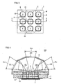
- FIG. 3 is a schematic plan view of the solid-state imaging element 3 in the compound-eye imaging device 100, showing unit images M formed on the solid-state imaging element 3.
- the solid-state imaging element 3 is formed of a CCD (Charge Coupled Device) image sensor or a CMOS (Complementary Metal Oxide Semiconductor) image sensor. As shown in FIG 3 , the solid-state imaging element 3 captures or forms, on a surface thereof, nine unit images M corresponding to and formed by the nine optical lenses L, respectively.
- FIG 3 shows a case where a letter "A" (as a target object to be captured) is captured as unit images M.
- each of the unit images M formed on the solid-state imaging element 3 by the respective optical lenses L has a shape of a circle
- each image extracted from the circular unit image M by the microprocessor 6 e.g. to produce a combined image from the respective image units M has a shape of a rectangle (which can be a square) which is inscribed in the circle.
- the microprocessor 6 extracts a rectangular image from each unit image M
- the microprocessor 6 removes portions of the each unit image M which are close to adjacent unit images M.
- FIG 3 shows each of such images N having a shape of rectangle (rectangular images N) as extracted by the microprocessor 6.
- the nine optical lenses L are arranged and integrated as an integrated group Q arranged in a rectangular pattern (which can be a square pattern).
- the stray light blocking member 11 surrounds the integrated group Q of optical lenses L as seen in plan view, and has a rectangular window 15 of a rectangle similar to an outer shape (rectangular shape) of the integrated group Q of optical lenses L.
- both sides of the rectangle of the rectangular window 15 are designated by Ta, Tb, and the distance of the stray light blocking member 11 from the plate-shaped stop member 9 is designated by D as shown in FIG 2 .
- These parameters Ta, Tb and D are set (selected) so that the respective lights passing through the stray light blocking member 11 and the stop apertures 8 and collected by the respective optical lenses L and further emitted from the respective optical lenses L to the solid-state imaging element 3 are prevented from entering unit images M other than the unit images M corresponding to the respective optical lenses L.
- Each optical lens L in the present embodiment has a view angle of about 30° (thirty degrees).
- FIG 1 shows an angular range ⁇ a (hereafter referred to as "effective incident view angle range”) of light collected by each optical lens L within a view angle (capture angle) of the optical lens L as well as an angular range ⁇ b (hereafter referred to as "effective exit view angle range”) of light emitted from the each optical lens L toward the solid-state imaging element 3 (after collected by the each optical lens L in the effective incident view angle range ⁇ a) to form each unit image M.
- the optical lens system 2 is designed so that the unit images M formed by lights each emitted from each optical lens L in the effective exit view angle range ⁇ b do not overlap each other (refer to FIG. 3 ).
- the parameters described above which are distance D of the stray light blocking member 11 from the plate-shaped stop member 9 and the lengths Ta, Tb of the sides of the rectangular window 15 of the stray light blocking member 11, are set so that the stray light blocking member 11 does not block light in the effective incident view angle range ⁇ a to pass through each of the optical lenses L.
- these parameters Ta, Tb and D are designed so that light coming from outside the effective incident view angle range ⁇ a and entering each optical lens L corresponding to each unit image M is prevented from entering a unit image M or images M adjacent to the each unit image M corresponding to the each optical lens L. This prevents lights passing through optical lenses corresponding to adjacent unit images from interfering with each other.
- FIG. 3 showing an area C in a rough grid pattern which is an area formed between the nine unit images M corresponding to the nine optical lenses L arranged in a matrix array of three rows and three columns in the compound-eye imaging device 100.
- the grid-patterned area C is an only possible area in which lights passing through adjacent optical lenses L diagonally from the front (i.e. from a target object to be captured), as shown e.g. by boundary lights La, Lb described below, may interfere with each other.
- a partial area C1 of the area C is used as a representative of the area C to consider and explain the area C.
- FIG. 1 is a cross-sectional view of the compound-eye imaging device 100 along line X-X shown in FIG. 3 which passes through the center of each of the unit images M (or optical lenses L or stop apertures 8 corresponding thereto) in the middle row of the matrix.
- FIG. 1 is a cross-sectional view of the compound-eye imaging device 100 along line X-X shown in FIG. 3 which passes through the center of each of the unit images M (or optical lenses L or stop apertures 8 corresponding thereto) in the middle row of the matrix.
- FIG. 1 shows a boundary light La which enters and passes through a right end of the rectangular window 15 and through a left end of the middle stop aperture 8 at an interface between the lens holder 7 (or the middle optical lens L) and the plate-shaped stop member 9 (or the middle stop aperture 8) at an incident angle of ⁇ .
- FIG. 1 also shows a boundary light Lb which enters and passes through a left end of the rectangular window 15 and through a right end of the left stop aperture 8 at an interface between the lens holder 7 (or the left optical lens L) and the plate-shaped stop member 9 (or the left stop aperture 8) at an incident angle of ⁇ .
- the middle (center) optical lens L might pass and emit light toward the left unit image M in the partial area C1 if such light had a lower incident angle than the boundary light La, that is an angle lower than ⁇ .
- such light (or stray light) which might enter the middle (center) optical lens L at an incident angle lower than ⁇ , is actually blocked by a right part 11R of the stray light blocking member 11, so that such light does not reach the left unit image M.
- the left unit image M is not interfered by such light (stray light).
- the left optical lens L might pass and emit light toward the middle (center) unit image M in the partial area C1 if such light had a lower incident angle than the boundary light Lb, that is an angle lower than ⁇ .
- such light .(or stray light) which might enter the left optical lens L at an incident angle lower than ⁇ , is actually blocked by a left part 11L of the stray light blocking member 11, so that such light does not reach the middle (center) unit image M.
- the middle unit image M is not interfered by such light (stray light).
- the interference between the upper row of three unit images M and the middle row of three unit images M is prevented by an upper part 11U and a lower part 11D of the stray light blocking member 11.
- the interference between the lower rows of three unit images M and the middle rows of three unit images M is prevented by the upper part 11U and the lower part 11D of the stray light blocking member 11.
- the stray light blocking member 11 having the rectangular window 15 similar to the integrated group Q of optical lenses L properly limits the incident angle of light entering each optical lens L for each unit image M so as to prevent the light entering the each optical lens L and emitted to the solid-state imaging element 3 from interfering with other unit images M (adjacent unit images M) than the each unit image M, thereby preventing degradation of each unit image M (particularly in peripheral portions of the each unit image M which are close to the adjacent unit images M).
- the microprocessor 6 when the microprocessor 6 produces a combined image from the respective unit images M, the microprocessor 6 extracts, from each circular unit image M, a rectangular image N to be used for the combined image. Since portions of each unit image M which are close and adjacent to other unit images M than the each unit image M and are likely to cause interference with such other unit images M are removed to produce each rectangular image N, the extraction of each rectangular image N for the production of a combined image also contributes to the prevention of degradation of the combined image.
- the stray light blocking member 11 having the rectangular window 15 similar to the integrated group Q of optical lenses L is provided on the capture zone side of the optical lenses L arranged in a rectangular pattern in a matrix of three rows and three columns.
- the stray light blocking member 11 is provided on the capture zone side, i.e. in a space which is relatively more open or wider than the narrow space between the solid-stating imaging element 3 and the optical lenses L, the manufacturing process can be prevented from being complicated.
- the housing of the compound-eye imaging device 100 can be designed to also serve as such stray light blocking member 11.
- FIG. 4 is a schematic cross-sectional view
- FIG 5 is a schematic plan view of the compound-eye imaging device 200.
- the compound-eye imaging device 200 of the second embodiment has substantially the same structure as that of the compound-eye imaging device 100 of the first embodiment except for the following.
- the number of optical lenses L of an optical system 2 is three, in which the three optical lenses L are arranged in one row, left, center and right (refer to FIG 5 ).
- stray light blocking member 21 has three windows 22L, 22C, 22R, rather than one window, which respectively correspond to lights entering the three optical lenses L.
- the stray light blocking member 21 is placed on the capture zone side of the optical lenses L relative to the 45-45-90 degree right-angle prisms 20L, 20R.
- the elements and parts of the compound-eye imaging device 200 having the structure the same as or similar to those of the compound-eye imaging device 100 are designated by the same or similar reference numerals and characters, omitting description thereof.
- the 45-45-90 right-angle prisms 20L, 20R serve to bend the propagation paths of lights to be collected on the left and right optical lenses L by roughly 80° (eighty degrees) so that lights each in a capture zone at an angle of roughly 10° (ten degrees) from the plane of a plate-shaped stop member 9 (or solid-state imaging element 3) are collected on the left and right optical lenses, respectively.
- FIG. 1 A plate-shaped stop member 9 (or solid-state imaging element 3)
- FIG. 4 shows an effective incident view angle range ⁇ c of light collected by each of the left and right optical lenses having a view angle of about 30° (thirty degrees), and an effective incident view angle range ⁇ a of light collected by the center optical lens also having a view angle of about 30°, in which the central axis of the effective incident view angle range ⁇ c (front range) is roughly 10° from the plane of a plate-shaped stop member 9 as described above.
- the stray light blocking member 21 is a dome-shaped member also serving as a housing of the compound-eye imaging device 200, and has three windows 22L, 22C, 22R formed not to block the lights in the effective incident view angle ranges ⁇ c, ⁇ a, ⁇ c for the three optical lenses L, respectively.
- incident lights in a range outside each of the effective incident view angle ranges ⁇ c (left range), ⁇ a (front range), ⁇ c (right range) are blocked by the dome-shaped stray light blocking member 21, and thus are prevented from being collected on the optical lenses L.
- the compound-eye imaging device 200 of the present embodiment can prevent the generation of stray light in each unit image M to interfere with adjacent unit images M, thereby preventing degradation of each unit image M without complicating the manufacturing process and increasing the cost thereof.
- the compound-eye imaging device 200 can capture images in the front range, left range and right range, each of about 30°, in the capture zone of 180°, it can be conveniently mounted on the rear of a vehicle to monitor the surroundings of the vehicle.
- FIG 6 is a schematic cross-sectional view
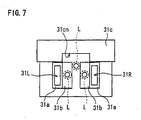
- FIG. 7 is a schematic plan view of the compound-eye imaging device 300.
- the compound-eye imaging device 300 of the third embodiment has substantially the same structure as that of the compound-eye imaging device 200 of the second embodiment except for the following.
- three optical lenses L are not arranged in a row, but are arranged at the vertexes of a triangle as seen in plan view (refer to FIG. 7 ).
- each of the optical lenses L is set to have a view angle of about 40° (forty degrees), while left and right 45-45-90 degree right angle prisms 30L, 30R are set to have a mounting angle ⁇ of about 25° (twenty-five) to the optical lenses L, respectively, so as to allow effective incident view angle ranges ⁇ c, ⁇ a, ⁇ c to continuously cover the range of about 120° in the front capture range of 180°, so that a panoramic image with a picture angle of 120° can be obtained by combining unit images M formed by the respective optical lenses L.
- a stray light blocking member 31 is formed of light blocking (shielding) films such as black films 31a, 31b attached to the left and right 45-45-90 degree right angle prisms 30L, 30R, respectively, and of a plate-shaped member 31c.
- the elements and parts of the compound-eye imaging device 300 having the structure the same as or similar to those of the compound-eye imaging device 200 are designated by the same or similar reference numerals and characters, omitting description thereof.
- the light blocking films 31a have rectangular windows 31L, 31R, and are each attached to one of the mutually perpendicular surfaces of the left and right 45-45-90 degree right angle prisms 30L, 30R, respectively, so as to block incident lights in a range outside each of the effective incident view angle ranges ⁇ c (left range) and ⁇ c (right range).
- the light blocking films 31b are attached to the mutually facing hypotenuses of the left and right 45-45-90 degree right angle prisms 30L, 30R, respectively.
- the windows 31L, 31R of the light blocking films 31a correspond to the windows 22L, 22R formed in the stray light blocking member 21 of the compound-eye imaging device 200 in the second embodiment of the present invention.
- the plate-shaped member 31c has a concave notch 31cn as seen in plan view (refer to FIG. 7 ), and is placed horizontally as viewed toward a target object to be imaged so that the concave notch 31cn covers around the optical lens L in the middle, covering an upper part of the optical lenses L as viewed toward the target object (namely as viewed in FIG 7 ).
- the plate-shaped member 31c blocks, in particular, light (stray light) coming from above as viewed in FIG 7 among incident lights in a range outside the effective incident view angle range ⁇ a of the optical lens L in the middle.
- the compound-eye imaging device 300 of the present embodiment can prevent the generation of stray light in each unit image M to interfere with adjacent unit images M, thereby preventing degradation of each unit image M without complicating the manufacturing process and increasing the cost thereof.
- the compound-eye imaging device 300 of the present embodiment makes it possible to obtain a panoramic image with a picture angle of 120° in the front range of the compound-eye imaging device 300.
- the present invention is not limited to the above embodiments, and various modifications are possible within the spirit and scope of the present invention.
- the light blocking films (black films) 31a, 31b attached to the ones of the mutually perpendicular surfaces and the hypotenuses of the left and right 45-45-90 degree right angle prisms 30L, 30R can be replaced by light blocking layers (black layers) printed on such surfaces and hypotenuses.
- such light blocking layers printed on the left and right 45-45-90 degree right angle prisms 30L, 30R correspond to the claimed "stray light blocking member".
Landscapes
- Engineering & Computer Science (AREA)
- Multimedia (AREA)
- Signal Processing (AREA)
- Studio Devices (AREA)
- Cameras In General (AREA)
- Transforming Light Signals Into Electric Signals (AREA)
Abstract
Description
- The present invention relates to a compound-eye imaging device.
- A compound-eye imaging device is known as an imaging device to realize a thin camera as disclosed, for example, in Japanese Laid-open Patent Publication
Hei 10-84104 Hei 10-84104 - Generally, in order to reduce the size of the compound-eye imaging device, the optical lenses are densely formed, and the unit images formed by the optical lenses are also formed close to each other on the solid-state imaging element. However, a compound-eye imaging device having densely formed optical lenses to form unit images close to each other has a disadvantage that light entering through each optical lens to form each unit image corresponding to the each optical lens may interfere with light (hereafter referred to as "stray light") entering through an adjacent optical lens or lenses, thereby degrading each unit image. This may cause a combined image or a panoramic image produced from the unit images to be no good.
- In order to overcome this disadvantage, it is known to provide, between the solid-state imaging element and the optical lenses, walls (spacers in the compound-eye imaging device of Japanese Laid-open Patent Publication
Hei 10-84104 - In addition, although components of light, which are emitted from each optical lens, and which have large emission angles and thus are likely to become stray light, are prevented by the provision of the walls from propagating any further to reach an adjacent unit image or images, the components of light reflected from the walls may reach the solid-state imaging element which is located in an area partitioned by the walls and which forms a unit image corresponding to the each optical lens, thereby interfering with and degrading such unit image itself. Thus, in order to prevent the generation of stray light and the degradation of each unit image, the wall surface of the walls is required to have an extremely low reflectance e.g. by selecting the material of the walls. However, this further complicates the manufacturing process and increases the cost of the compound-eye imaging device.
- An object of the present invention is to provide a compound-eye imaging device which can prevent the generation of stray light without complicating the manufacturing process and increasing the cost thereof, and can obtain a good quality image without interference by the stray light.
- This object is achieved according to the present invention by a compound-eye imaging device comprising: multiple optical lenses for collecting light in a capture zone; a solid-state imaging element for capturing, on a surface thereof, unit images formed by the multiple optical lenses, respectively; and a stray light blocking member provided on a capture zone side of the optical lenses for limiting an incident angle of light entering each optical lens for each unit image so as to prevent the light entering the each optical lens and emitted to the solid-state imaging element from interfering with other unit images than the each unit image.
- The thus structured compound-eye imaging device of the present invention has the stray light blocking member provided on the capture zone side of the optical lenses, thereby eliminating the need to provide walls between the solid-state imaging element and the optical lenses, so that it can prevent the generation of stray light without complicating the manufacturing process and increasing the cost thereof, and can easily obtain a good quality image without interference by the stray light.
- The compound-eye imaging device can further comprise a prism placed on the capture zone side of the optical lenses for changing propagation paths of lights to be collected on the optical lenses, wherein the stray light blocking member is placed on the capture zone side relative to the prism. Since the stray light blocking member is placed on the capture zone side relative to the prism, it can be mounted in the compound-eye imaging device without complicating the manufacturing process and increasing the cost thereof.
- The stray light blocking member can be a film attached to a surface of the prism or a layer printed on the prism. This makes it possible to further reduce the size of the entire compound-eye imaging device.
- The compound-eye imaging device can further be designed so that the optical lenses are arranged as an integrated group in a matrix array of rows and columns, wherein the stray light blocking member surrounds the integrated group of optical lenses as seen in plan view, and has a rectangular window of a rectangle similar to an outer shape of the integrated group of optical lenses.
- While the novel features of the present invention are set forth in the appended claims, the present invention will be better understood from the following detailed description taken in conjunction with the drawings.
- The present invention will be described hereinafter with reference to the annexed drawings. It is to be noted that all the drawings are shown for the purpose of illustrating the technical concept of the present invention or embodiments thereof, wherein:
-
FIG 1 is a schematic cross-sectional view of a compound-eye imaging device according to a first embodiment of the present invention; -
FIG. 2 is a schematic perspective view of the compound-eye imaging device; -
FIG 3 is a schematic plan view of a solid-state imaging element in the compound-eye imaging device, showing unit images formed on the solid-state imaging element; -
FIG. 4 is a schematic cross-sectional view of a compound-eye imaging device according to a second embodiment of the present invention; -
FIG 5 is a schematic plan view of the compound-eye imaging device; -
FIG. 6 is a schematic cross-sectional view of a compound-eye imaging device according to a third embodiment of the present invention; and -
FIG. 7 is a schematic plan view of the compound-eye imaging device. - Embodiments of the present invention, as best mode for carrying out the invention, will be described hereinafter with reference to the drawings. The present invention relates to a compound-eye imaging device. It is to be understood that the embodiments described herein are not intended as limiting, or encompassing the entire scope of, the present invention. Note that like parts are designated by like reference numerals, characters or symbols throughout the drawings.
- Referring to
FIG. 1 to FIG 3 , a compound-eye imaging device 100 according to a first embodiment of the present invention will be described.FIG 1 is a schematic cross-sectional view (along line X-X shown inFIG. 3 ) andFIG. 2 is a schematic perspective view of the compound-eye imaging device 100. As shown inFIG 1 , the compound-eye imaging device 100 comprises in a housing (not shown) thereof: anoptical system 2 including optical lenses M, described later, for collecting light in a capture zone to form multiple unit images on a predetermined focal plane; and a solid-state imaging element 3 placed at the focal plane of theoptical lens system 2 for converting the multiple unit images formed by theoptical lens system 2 to electronic image information. The compound-eye imaging device 100 further comprises: an A/D (Analog-to-Digital)converter 4 for converting the electronic image information to digital information; a DSP (Digital Signal Processor) 5 for receiving the digital information (unit images) from the A/D converter 4; and a microprocessor 6 for subjecting the image information (unit images) received by the DSP 5 to image processes, such as an image extracting process and an image combining process, so as to produce one combined image. - The
optical lens system 2 is held in one plane by alens holder 7, and comprises nine optical lenses L (refer toFIG. 2 ) arranged in a matrix array of three rows and three columns, and a plate-shaped stop member 9 having ninestop apertures 8 at positions corresponding to the optical lenses L, respectively. Theoptical lens system 2 further comprises: a stray light blocking member 11 provided at a position distant from the plate-shaped stop member 9 by a predetermined distance D for limiting the incident angle of light entering eachstop aperture 8 in the capture zone; afilter 12 for cutting off a near infrared range of light emitted from each optical lens L toward the solid-state imaging element 3; and acover glass 13 for covering the solid-state imaging element 3. Thefilter 12 is held by aholder member 14 in a hollow portion of theholder member 14 which is fixed to a lower surface of thelens holder 7, while thecover glass 13 is supported by a lower surface of theholder member 14. It is to be noted that the stray light blocking member 11 is provided on the capture zone side, i.e. in a space which is relatively more open or wider than the narrow space between the solid-statingimaging element 3 and the optical lenses L, preventing complication of the manufacturing process. -
FIG. 3 is a schematic plan view of the solid-state imaging element 3 in the compound-eye imaging device 100, showing unit images M formed on the solid-state imaging element 3. The solid-state imaging element 3 is formed of a CCD (Charge Coupled Device) image sensor or a CMOS (Complementary Metal Oxide Semiconductor) image sensor. As shown inFIG 3 , the solid-state imaging element 3 captures or forms, on a surface thereof, nine unit images M corresponding to and formed by the nine optical lenses L, respectively.FIG 3 shows a case where a letter "A" (as a target object to be captured) is captured as unit images M. Although each of the unit images M formed on the solid-state imaging element 3 by the respective optical lenses L has a shape of a circle, each image extracted from the circular unit image M by the microprocessor 6 e.g. to produce a combined image from the respective image units M has a shape of a rectangle (which can be a square) which is inscribed in the circle. When the microprocessor 6 extracts a rectangular image from each unit image M, the microprocessor 6 removes portions of the each unit image M which are close to adjacent unit images M.FIG 3 shows each of such images N having a shape of rectangle (rectangular images N) as extracted by the microprocessor 6. - As shown in
FIG 2 , the nine optical lenses L are arranged and integrated as an integrated group Q arranged in a rectangular pattern (which can be a square pattern). The stray light blocking member 11 surrounds the integrated group Q of optical lenses L as seen in plan view, and has arectangular window 15 of a rectangle similar to an outer shape (rectangular shape) of the integrated group Q of optical lenses L. Here, both sides of the rectangle of therectangular window 15 are designated by Ta, Tb, and the distance of the stray light blocking member 11 from the plate-shaped stop member 9 is designated by D as shown inFIG 2 . These parameters Ta, Tb and D are set (selected) so that the respective lights passing through the stray light blocking member 11 and thestop apertures 8 and collected by the respective optical lenses L and further emitted from the respective optical lenses L to the solid-state imaging element 3 are prevented from entering unit images M other than the unit images M corresponding to the respective optical lenses L. - Referring back to
FIG 1 , these parameters Ta, Tb and D will be described in more detail. Each optical lens L in the present embodiment has a view angle of about 30° (thirty degrees).FIG 1 shows an angular range θa (hereafter referred to as "effective incident view angle range") of light collected by each optical lens L within a view angle (capture angle) of the optical lens L as well as an angular range θb (hereafter referred to as "effective exit view angle range") of light emitted from the each optical lens L toward the solid-state imaging element 3 (after collected by the each optical lens L in the effective incident view angle range θa) to form each unit image M. Theoptical lens system 2 is designed so that the unit images M formed by lights each emitted from each optical lens L in the effective exit view angle range θb do not overlap each other (refer toFIG. 3 ). - Furthermore, the parameters described above, which are distance D of the stray light blocking member 11 from the plate-
shaped stop member 9 and the lengths Ta, Tb of the sides of therectangular window 15 of the stray light blocking member 11, are set so that the stray light blocking member 11 does not block light in the effective incident view angle range θa to pass through each of the optical lenses L. In addition, these parameters Ta, Tb and D are designed so that light coming from outside the effective incident view angle range θa and entering each optical lens L corresponding to each unit image M is prevented from entering a unit image M or images M adjacent to the each unit image M corresponding to the each optical lens L. This prevents lights passing through optical lenses corresponding to adjacent unit images from interfering with each other. - This can be explained with reference to
FIG. 3 showing an area C in a rough grid pattern which is an area formed between the nine unit images M corresponding to the nine optical lenses L arranged in a matrix array of three rows and three columns in the compound-eye imaging device 100. Due to the design of the parameters Ta, Tb (lengths) and D (distance) described above, the grid-patterned area C is an only possible area in which lights passing through adjacent optical lenses L diagonally from the front (i.e. from a target object to be captured), as shown e.g. by boundary lights La, Lb described below, may interfere with each other. A partial area C1 of the area C is used as a representative of the area C to consider and explain the area C. - Referring to
FIG. 3 , the partial area C1 to be considered here is positioned between the left and middle (center) unit images M in the middle row among the nine unit images M in the matrix of three rows and three columns.FIG. 1 is a cross-sectional view of the compound-eye imaging device 100 along line X-X shown inFIG. 3 which passes through the center of each of the unit images M (or optical lenses L or stopapertures 8 corresponding thereto) in the middle row of the matrix.FIG. 1 shows a boundary light La which enters and passes through a right end of therectangular window 15 and through a left end of themiddle stop aperture 8 at an interface between the lens holder 7 (or the middle optical lens L) and the plate-shaped stop member 9 (or the middle stop aperture 8) at an incident angle of α.FIG. 1 also shows a boundary light Lb which enters and passes through a left end of therectangular window 15 and through a right end of theleft stop aperture 8 at an interface between the lens holder 7 (or the left optical lens L) and the plate-shaped stop member 9 (or the left stop aperture 8) at an incident angle of β. - Now, referring to
FIG. 1 andFIG 3 , the middle (center) optical lens L might pass and emit light toward the left unit image M in the partial area C1 if such light had a lower incident angle than the boundary light La, that is an angle lower than α. However, as shown inFIG. 1 , such light (or stray light), which might enter the middle (center) optical lens L at an incident angle lower than α, is actually blocked by aright part 11R of the stray light blocking member 11, so that such light does not reach the left unit image M. Thus, the left unit image M is not interfered by such light (stray light). Similarly, the left optical lens L might pass and emit light toward the middle (center) unit image M in the partial area C1 if such light had a lower incident angle than the boundary light Lb, that is an angle lower than β. However, as shown inFIG 1 , such light .(or stray light), which might enter the left optical lens L at an incident angle lower than β, is actually blocked by aleft part 11L of the stray light blocking member 11, so that such light does not reach the middle (center) unit image M. Thus, the middle unit image M is not interfered by such light (stray light). - This similarly applies to the other partial areas of the area C. For example, in partial areas C2 and C3 shown in
FIG. 3 , light (stray light) which might interfere with the left unit images M is blocked by theright part 11R of the stray light blocking member 11, while light (stray light) which might interfere with the middle unit images M is blocked by theleft part 11L of the stray light blocking member 11. In other words, the interference between the left column of three unit images M and the middle column of three unit images M is prevented by theright part 11R and theleft part 11L of the stray light blocking member 11. Likewise, the interference between the right column of three unit images M and the middle column of three unit images M is prevented by theright part 11R and theleft part 11L of the stray light blocking member 11. Quite similarly, the interference between the upper row of three unit images M and the middle row of three unit images M is prevented by anupper part 11U and alower part 11D of the stray light blocking member 11. On the other hand, the interference between the lower rows of three unit images M and the middle rows of three unit images M is prevented by theupper part 11U and thelower part 11D of the stray light blocking member 11. - In short, according to the compound-
eye imaging device 100 of the present embodiment having optical lenses L integrated as an integrated group Q arranged in a rectangular pattern in a matrix of three rows and three columns, the stray light blocking member 11 having therectangular window 15 similar to the integrated group Q of optical lenses L properly limits the incident angle of light entering each optical lens L for each unit image M so as to prevent the light entering the each optical lens L and emitted to the solid-state imaging element 3 from interfering with other unit images M (adjacent unit images M) than the each unit image M, thereby preventing degradation of each unit image M (particularly in peripheral portions of the each unit image M which are close to the adjacent unit images M). - In addition, according to the compound-
eye imaging device 100 of the present embodiment, when the microprocessor 6 produces a combined image from the respective unit images M, the microprocessor 6 extracts, from each circular unit image M, a rectangular image N to be used for the combined image. Since portions of each unit image M which are close and adjacent to other unit images M than the each unit image M and are likely to cause interference with such other unit images M are removed to produce each rectangular image N, the extraction of each rectangular image N for the production of a combined image also contributes to the prevention of degradation of the combined image. - As described in the foregoing, according to the compound-
eye imaging device 100 of the present embodiment, the stray light blocking member 11 having therectangular window 15 similar to the integrated group Q of optical lenses L is provided on the capture zone side of the optical lenses L arranged in a rectangular pattern in a matrix of three rows and three columns. Thus, the generation of stray light in each unit image M to interfere with adjacent unit images M can be properly prevented. In addition, since the stray light blocking member 11 is provided on the capture zone side, i.e. in a space which is relatively more open or wider than the narrow space between the solid-statingimaging element 3 and the optical lenses L, the manufacturing process can be prevented from being complicated. Note that the housing of the compound-eye imaging device 100 can be designed to also serve as such stray light blocking member 11. - Referring to
FIG. 4 andFIG 5 , a compound-eye imaging device 200 according to a second embodiment of the present invention will be described below.FIG 4 is a schematic cross-sectional view andFIG 5 is a schematic plan view of the compound-eye imaging device 200. The compound-eye imaging device 200 of the second embodiment has substantially the same structure as that of the compound-eye imaging device 100 of the first embodiment except for the following. First, in the compound-eye imaging device 200, the number of optical lenses L of anoptical system 2 is three, in which the three optical lenses L are arranged in one row, left, center and right (refer toFIG 5 ). - Second, 45-45-90 degree right-
angle prisms light blocking member 21 has threewindows light blocking member 21 is placed on the capture zone side of the optical lenses L relative to the 45-45-90 degree right-angle prisms eye imaging device 200 having the structure the same as or similar to those of the compound-eye imaging device 100 are designated by the same or similar reference numerals and characters, omitting description thereof. - The 45-45-90 right-
angle prisms FIG. 4 shows an effective incident view angle range θc of light collected by each of the left and right optical lenses having a view angle of about 30° (thirty degrees), and an effective incident view angle range θa of light collected by the center optical lens also having a view angle of about 30°, in which the central axis of the effective incident view angle range θc (front range) is roughly 10° from the plane of a plate-shapedstop member 9 as described above. - As shown in
FIG 4 , the straylight blocking member 21 is a dome-shaped member also serving as a housing of the compound-eye imaging device 200, and has threewindows light blocking member 21, and thus are prevented from being collected on the optical lenses L. Thus, similarly as in the compound-eye imaging device 100 of the fist embodiment, the compound-eye imaging device 200 of the present embodiment can prevent the generation of stray light in each unit image M to interfere with adjacent unit images M, thereby preventing degradation of each unit image M without complicating the manufacturing process and increasing the cost thereof. Note that since the compound-eye imaging device 200 can capture images in the front range, left range and right range, each of about 30°, in the capture zone of 180°, it can be conveniently mounted on the rear of a vehicle to monitor the surroundings of the vehicle. - Referring now to
FIG 6 andFIG 7 , a compound-eye imaging device 300 according to a third embodiment of the present invention will be described hereinafter.FIG 6 is a schematic cross-sectional view andFIG. 7 is a schematic plan view of the compound-eye imaging device 300. The compound-eye imaging device 300 of the third embodiment has substantially the same structure as that of the compound-eye imaging device 200 of the second embodiment except for the following. First, in the compound-eye imaging device 300, three optical lenses L are not arranged in a row, but are arranged at the vertexes of a triangle as seen in plan view (refer toFIG. 7 ). - Second, each of the optical lenses L is set to have a view angle of about 40° (forty degrees), while left and right 45-45-90 degree
right angle prisms black films right angle prisms member 31c. The elements and parts of the compound-eye imaging device 300 having the structure the same as or similar to those of the compound-eye imaging device 200 are designated by the same or similar reference numerals and characters, omitting description thereof. - The
light blocking films 31a haverectangular windows right angle prisms light blocking films 31b are attached to the mutually facing hypotenuses of the left and right 45-45-90 degreeright angle prisms windows light blocking films 31a correspond to thewindows light blocking member 21 of the compound-eye imaging device 200 in the second embodiment of the present invention. - The plate-shaped
member 31c has a concave notch 31cn as seen in plan view (refer toFIG. 7 ), and is placed horizontally as viewed toward a target object to be imaged so that the concave notch 31cn covers around the optical lens L in the middle, covering an upper part of the optical lenses L as viewed toward the target object (namely as viewed inFIG 7 ). Thus, the plate-shapedmember 31c blocks, in particular, light (stray light) coming from above as viewed inFIG 7 among incident lights in a range outside the effective incident view angle range θa of the optical lens L in the middle. Thus, similarly as in the compound-eye imaging devices eye imaging device 300 of the present embodiment can prevent the generation of stray light in each unit image M to interfere with adjacent unit images M, thereby preventing degradation of each unit image M without complicating the manufacturing process and increasing the cost thereof. In addition; the compound-eye imaging device 300 of the present embodiment makes it possible to obtain a panoramic image with a picture angle of 120° in the front range of the compound-eye imaging device 300. - It is to be noted that the present invention is not limited to the above embodiments, and various modifications are possible within the spirit and scope of the present invention. For example, the light blocking films (black films) 31a, 31b attached to the ones of the mutually perpendicular surfaces and the hypotenuses of the left and right 45-45-90 degree
right angle prisms right angle prisms - The present invention has been described above using presently preferred embodiments, but such description should not be interpreted as limiting the present invention. Various modifications will become obvious, evident or apparent to those ordinarily skilled in the art, who have read the description. Accordingly, the appended claims should be interpreted to cover all modifications and alterations which fall within the spirit and scope of the present invention.
- This application is based on Japanese patent application
2007-186658 filed July 18, 2007
Claims (5)
- A compound-eye imaging device comprising:multiple optical lenses for collecting light in a capture zone;a solid-state imaging element for capturing, on a surface thereof, unit images formed by the multiple optical lenses, respectively; anda stray light blocking member provided on a capture zone side of the optical lenses for limiting an incident angle of light entering each optical lens for each unit image so as to prevent the light entering the each optical lens and emitted to the solid-state imaging element from interfering with other unit images than the each unit image.
- The compound-eye imaging device according to claim 1,
which further comprises a prism placed on the capture zone side of the optical lenses for changing propagation paths of lights to be collected on the optical lenses,
wherein the stray light blocking member is placed on the capture zone side relative to the prism. - The compound-eye imaging device according to claim 2,
wherein the stray light blocking member is a film attached to a surface of the prism. - The compound-eye imaging device according to claim 2,
wherein the stray light blocking member is a layer printed on the prism. - The compound-eye imaging device according claim 1,
wherein the optical lenses are arranged as an integrated group in a matrix array of rows and columns, and
wherein the stray light blocking member surrounds the integrated group of optical lenses as seen in plan view, and has a rectangular window of a rectangle similar to an outer shape of the integrated group of optical lenses.
Applications Claiming Priority (1)
| Application Number | Priority Date | Filing Date | Title |
|---|---|---|---|
| JP2007186658A JP4412362B2 (en) | 2007-07-18 | 2007-07-18 | Compound eye imaging device |
Publications (1)
| Publication Number | Publication Date |
|---|---|
| EP2018044A1 true EP2018044A1 (en) | 2009-01-21 |
Family
ID=39743042
Family Applications (1)
| Application Number | Title | Priority Date | Filing Date |
|---|---|---|---|
| EP08013021A Withdrawn EP2018044A1 (en) | 2007-07-18 | 2008-07-18 | Compound-eye imaging device |
Country Status (3)
| Country | Link |
|---|---|
| US (1) | US7700904B2 (en) |
| EP (1) | EP2018044A1 (en) |
| JP (1) | JP4412362B2 (en) |
Cited By (1)
| Publication number | Priority date | Publication date | Assignee | Title |
|---|---|---|---|---|
| WO2020150908A1 (en) * | 2019-01-22 | 2020-07-30 | SZ DJI Technology Co., Ltd. | Image sensor and fabrication method thereof |
Families Citing this family (41)
| Publication number | Priority date | Publication date | Assignee | Title |
|---|---|---|---|---|
| US9330324B2 (en) | 2005-10-11 | 2016-05-03 | Apple Inc. | Error compensation in three-dimensional mapping |
| EP1934945A4 (en) | 2005-10-11 | 2016-01-20 | Apple Inc | METHOD AND SYSTEM FOR RECONSTRUCTING AN OBJECT |
| US20110096182A1 (en) * | 2009-10-25 | 2011-04-28 | Prime Sense Ltd | Error Compensation in Three-Dimensional Mapping |
| US8390821B2 (en) | 2005-10-11 | 2013-03-05 | Primesense Ltd. | Three-dimensional sensing using speckle patterns |
| US8374397B2 (en) | 2005-10-11 | 2013-02-12 | Primesense Ltd | Depth-varying light fields for three dimensional sensing |
| US8494252B2 (en) | 2007-06-19 | 2013-07-23 | Primesense Ltd. | Depth mapping using optical elements having non-uniform focal characteristics |
| EP2235584B1 (en) * | 2008-01-21 | 2020-09-16 | Apple Inc. | Optical designs for zero order reduction |
| US8384997B2 (en) * | 2008-01-21 | 2013-02-26 | Primesense Ltd | Optical pattern projection |
| US8456517B2 (en) | 2008-07-09 | 2013-06-04 | Primesense Ltd. | Integrated processor for 3D mapping |
| JP5105482B2 (en) * | 2008-09-01 | 2012-12-26 | 船井電機株式会社 | Optical condition design method and compound eye imaging apparatus |
| US8462207B2 (en) | 2009-02-12 | 2013-06-11 | Primesense Ltd. | Depth ranging with Moiré patterns |
| US8786682B2 (en) | 2009-03-05 | 2014-07-22 | Primesense Ltd. | Reference image techniques for three-dimensional sensing |
| US8717417B2 (en) | 2009-04-16 | 2014-05-06 | Primesense Ltd. | Three-dimensional mapping and imaging |
| WO2011013079A1 (en) | 2009-07-30 | 2011-02-03 | Primesense Ltd. | Depth mapping based on pattern matching and stereoscopic information |
| JP5588310B2 (en) * | 2009-11-15 | 2014-09-10 | プライムセンス リミテッド | Optical projector with beam monitor |
| US20110115916A1 (en) * | 2009-11-16 | 2011-05-19 | Eiji Yafuso | System for mosaic image acquisition |
| US8830227B2 (en) * | 2009-12-06 | 2014-09-09 | Primesense Ltd. | Depth-based gain control |
| JP2011150100A (en) * | 2010-01-21 | 2011-08-04 | Nippon Sheet Glass Co Ltd | Erecting equal-magnification lens array plate and image reading device |
| US20110187878A1 (en) * | 2010-02-02 | 2011-08-04 | Primesense Ltd. | Synchronization of projected illumination with rolling shutter of image sensor |
| US20110188054A1 (en) * | 2010-02-02 | 2011-08-04 | Primesense Ltd | Integrated photonics module for optical projection |
| US8982182B2 (en) | 2010-03-01 | 2015-03-17 | Apple Inc. | Non-uniform spatial resource allocation for depth mapping |
| US9036158B2 (en) | 2010-08-11 | 2015-05-19 | Apple Inc. | Pattern projector |
| WO2012020380A1 (en) | 2010-08-11 | 2012-02-16 | Primesense Ltd. | Scanning projectors and image capture modules for 3d mapping |
| EP2643659B1 (en) | 2010-11-19 | 2019-12-25 | Apple Inc. | Depth mapping using time-coded illumination |
| CN102081296B (en) * | 2010-12-01 | 2012-11-07 | 南京航空航天大学 | Device and method for quickly positioning compound-eye vision imitated moving target and synchronously acquiring panoramagram |
| US9167138B2 (en) | 2010-12-06 | 2015-10-20 | Apple Inc. | Pattern projection and imaging using lens arrays |
| US9030528B2 (en) | 2011-04-04 | 2015-05-12 | Apple Inc. | Multi-zone imaging sensor and lens array |
| US8908277B2 (en) | 2011-08-09 | 2014-12-09 | Apple Inc | Lens array projector |
| US8749796B2 (en) | 2011-08-09 | 2014-06-10 | Primesense Ltd. | Projectors of structured light |
| US9157790B2 (en) | 2012-02-15 | 2015-10-13 | Apple Inc. | Integrated optoelectronic modules with transmitter, receiver and beam-combining optics for aligning a beam axis with a collection axis |
| AU2013237062B2 (en) | 2012-03-22 | 2015-07-16 | Apple Inc. | Diffraction-based sensing of mirror position |
| US9528906B1 (en) | 2013-12-19 | 2016-12-27 | Apple Inc. | Monitoring DOE performance using total internal reflection |
| US10012831B2 (en) | 2015-08-03 | 2018-07-03 | Apple Inc. | Optical monitoring of scan parameters |
| DE102015215833A1 (en) * | 2015-08-19 | 2017-02-23 | Fraunhofer-Gesellschaft zur Förderung der angewandten Forschung e.V. | Multi-aperture imaging device with optical substrate |
| DE102016204148A1 (en) * | 2016-03-14 | 2017-09-14 | Fraunhofer-Gesellschaft zur Förderung der angewandten Forschung e.V. | Multi-aperture imaging apparatus, imaging system and method for detecting an object area |
| US10073004B2 (en) | 2016-09-19 | 2018-09-11 | Apple Inc. | DOE defect monitoring utilizing total internal reflection |
| US11422292B1 (en) | 2018-06-10 | 2022-08-23 | Apple Inc. | Super-blazed diffractive optical elements with sub-wavelength structures |
| US11681019B2 (en) | 2019-09-18 | 2023-06-20 | Apple Inc. | Optical module with stray light baffle |
| US11506762B1 (en) | 2019-09-24 | 2022-11-22 | Apple Inc. | Optical module comprising an optical waveguide with reference light path |
| US11754767B1 (en) | 2020-03-05 | 2023-09-12 | Apple Inc. | Display with overlaid waveguide |
| WO2022197339A1 (en) | 2021-03-17 | 2022-09-22 | Apple Inc. | Waveguide-based transmitters with adjustable lighting |
Citations (4)
| Publication number | Priority date | Publication date | Assignee | Title |
|---|---|---|---|---|
| DE1016033B (en) * | 1954-07-03 | 1957-09-19 | Leitz Ernst Gmbh | Device for taking or playing back panoramic images |
| EP0813079A2 (en) * | 1996-06-14 | 1997-12-17 | Eastman Kodak Company | A diffractive/refractive lenslet array incorporating a second aspheric surface |
| US20070090275A1 (en) * | 2005-10-17 | 2007-04-26 | Funai Electric Co., Ltd. | Compound-Eye Imaging Device |
| JP2007186658A (en) | 2006-01-16 | 2007-07-26 | Bridgestone Corp | Primer for elastic pavement |
Family Cites Families (5)
| Publication number | Priority date | Publication date | Assignee | Title |
|---|---|---|---|---|
| JPS61289321A (en) | 1985-06-17 | 1986-12-19 | Fujitsu Ltd | Lens array with cylinder |
| JPH0286276A (en) | 1988-09-21 | 1990-03-27 | Nec Corp | Light collecting device for solid-state image pickup element |
| JPH03175403A (en) | 1989-12-05 | 1991-07-30 | Minolta Camera Co Ltd | Solid-state image pickup device |
| US7423679B2 (en) * | 2002-12-20 | 2008-09-09 | Eastman Kodak Company | Imaging system having extended useful latitude |
| US7375312B2 (en) * | 2005-01-26 | 2008-05-20 | Avago Technologies Ecbu Ip Pte Ltd | Planar fly's eye detector |
-
2007
- 2007-07-18 JP JP2007186658A patent/JP4412362B2/en not_active Expired - Fee Related
-
2008
- 2008-07-17 US US12/175,372 patent/US7700904B2/en not_active Expired - Fee Related
- 2008-07-18 EP EP08013021A patent/EP2018044A1/en not_active Withdrawn
Patent Citations (5)
| Publication number | Priority date | Publication date | Assignee | Title |
|---|---|---|---|---|
| DE1016033B (en) * | 1954-07-03 | 1957-09-19 | Leitz Ernst Gmbh | Device for taking or playing back panoramic images |
| EP0813079A2 (en) * | 1996-06-14 | 1997-12-17 | Eastman Kodak Company | A diffractive/refractive lenslet array incorporating a second aspheric surface |
| JPH1084104A (en) | 1996-06-14 | 1998-03-31 | Eastman Kodak Co | Image sensor |
| US20070090275A1 (en) * | 2005-10-17 | 2007-04-26 | Funai Electric Co., Ltd. | Compound-Eye Imaging Device |
| JP2007186658A (en) | 2006-01-16 | 2007-07-26 | Bridgestone Corp | Primer for elastic pavement |
Cited By (1)
| Publication number | Priority date | Publication date | Assignee | Title |
|---|---|---|---|---|
| WO2020150908A1 (en) * | 2019-01-22 | 2020-07-30 | SZ DJI Technology Co., Ltd. | Image sensor and fabrication method thereof |
Also Published As
| Publication number | Publication date |
|---|---|
| US20090021837A1 (en) | 2009-01-22 |
| JP2009027311A (en) | 2009-02-05 |
| JP4412362B2 (en) | 2010-02-10 |
| US7700904B2 (en) | 2010-04-20 |
Similar Documents
| Publication | Publication Date | Title |
|---|---|---|
| US7700904B2 (en) | Compound-eye imaging device | |
| JP4138867B2 (en) | Compound eye camera module | |
| US8094183B2 (en) | Panoramic imaging device | |
| EP1847873B1 (en) | Panoramic imaging device | |
| US8194169B2 (en) | Compound eye camera module and method of producing the same | |
| US20080297612A1 (en) | Image pickup device | |
| JP4374078B2 (en) | Compound eye camera module | |
| US7924342B2 (en) | Image sensor with image-capturing pixels and focus detection pixel areas and method for manufacturing image sensor | |
| EP1883223B1 (en) | Motion detection imaging device | |
| WO2007125761A1 (en) | Compound eye camera module | |
| JP6700402B2 (en) | Fingerprint authentication sensor module and fingerprint authentication device | |
| JP2018056522A (en) | Imaging element and focus adjustment device | |
| JP2010219571A (en) | Camera module | |
| TWI919208B (en) | Light path folding module, camera module and electronic device | |
| JP2002171429A (en) | Compound eye imaging system, imaging device, and electronic device | |
| JP5742272B2 (en) | Compound eye imaging device | |
| JP2005031460A (en) | Compound eye optical system | |
| JP2009180976A (en) | Compound eye camera module | |
| JP2004336228A (en) | Lens array device | |
| JP6127973B2 (en) | IMAGING DEVICE AND IMAGING ELEMENT FOR IMAGING DEVICE | |
| JPH05100186A (en) | Image sensor | |
| JP2007096825A (en) | Compound eye imaging apparatus | |
| JP5711351B2 (en) | Imaging apparatus and image processing method | |
| JP5537618B2 (en) | Imaging device | |
| JP2009210951A (en) | Imaging apparatus |
Legal Events
| Date | Code | Title | Description |
|---|---|---|---|
| PUAI | Public reference made under article 153(3) epc to a published international application that has entered the european phase |
Free format text: ORIGINAL CODE: 0009012 |
|
| AK | Designated contracting states |
Kind code of ref document: A1 Designated state(s): AT BE BG CH CY CZ DE DK EE ES FI FR GB GR HR HU IE IS IT LI LT LU LV MC MT NL NO PL PT RO SE SI SK TR |
|
| AX | Request for extension of the european patent |
Extension state: AL BA MK RS |
|
| 17P | Request for examination filed |
Effective date: 20090306 |
|
| AKX | Designation fees paid |
Designated state(s): DE FR GB |
|
| GRAP | Despatch of communication of intention to grant a patent |
Free format text: ORIGINAL CODE: EPIDOSNIGR1 |
|
| STAA | Information on the status of an ep patent application or granted ep patent |
Free format text: STATUS: THE APPLICATION IS DEEMED TO BE WITHDRAWN |
|
| 18D | Application deemed to be withdrawn |
Effective date: 20101125 |