EP2017900A2 - Leuchtdiode mit verbesserter Struktur - Google Patents
Leuchtdiode mit verbesserter Struktur Download PDFInfo
- Publication number
- EP2017900A2 EP2017900A2 EP08011718A EP08011718A EP2017900A2 EP 2017900 A2 EP2017900 A2 EP 2017900A2 EP 08011718 A EP08011718 A EP 08011718A EP 08011718 A EP08011718 A EP 08011718A EP 2017900 A2 EP2017900 A2 EP 2017900A2
- Authority
- EP
- European Patent Office
- Prior art keywords
- layer
- type
- hole injection
- holes
- type clad
- Prior art date
- Legal status (The legal status is an assumption and is not a legal conclusion. Google has not performed a legal analysis and makes no representation as to the accuracy of the status listed.)
- Granted
Links
Images
Classifications
-
- H—ELECTRICITY
- H10—SEMICONDUCTOR DEVICES; ELECTRIC SOLID-STATE DEVICES NOT OTHERWISE PROVIDED FOR
- H10H—INORGANIC LIGHT-EMITTING SEMICONDUCTOR DEVICES HAVING POTENTIAL BARRIERS
- H10H20/00—Individual inorganic light-emitting semiconductor devices having potential barriers, e.g. light-emitting diodes [LED]
- H10H20/80—Constructional details
- H10H20/81—Bodies
- H10H20/816—Bodies having carrier transport control structures, e.g. highly-doped semiconductor layers or current-blocking structures
-
- H—ELECTRICITY
- H10—SEMICONDUCTOR DEVICES; ELECTRIC SOLID-STATE DEVICES NOT OTHERWISE PROVIDED FOR
- H10H—INORGANIC LIGHT-EMITTING SEMICONDUCTOR DEVICES HAVING POTENTIAL BARRIERS
- H10H20/00—Individual inorganic light-emitting semiconductor devices having potential barriers, e.g. light-emitting diodes [LED]
- H10H20/80—Constructional details
- H10H20/81—Bodies
- H10H20/822—Materials of the light-emitting regions
- H10H20/824—Materials of the light-emitting regions comprising only Group III-V materials, e.g. GaP
- H10H20/825—Materials of the light-emitting regions comprising only Group III-V materials, e.g. GaP containing nitrogen, e.g. GaN
- H10H20/8252—Materials of the light-emitting regions comprising only Group III-V materials, e.g. GaP containing nitrogen, e.g. GaN characterised by the dopants
Definitions
- the present invention relates to a light emitting diode, and more particularly, to a light emitting diode with an improved laminated structure of a P-type semiconductor layer for smoothly injecting holes into an active layer.
- Group III element nitrides such as GaN, AlN and InGaN
- LEDs light emitting diodes
- an InGaN compound semiconductor has been considerably noticed due to its narrow band gap. LEDs using such a GaN-based compound semiconductor are used in various applications such as large sized full color flat panel displays, backlight sources, traffic lights, indoor illumination, high density light sources, high resolution output systems and optical communications.
- An LED generally has a structure in which an active layer is interposed between an N-type semiconductor layer and a P-type semiconductor layer. Electrons and holes are injected into the active layer from the N-type and P-type semiconductor layers, respectively, and the electrons and holes are recombined in the active layer, thereby emitting light.
- impurities from the P-type semiconductor layer are diffused into the active layer, and therefore, the active layer may be deteriorated.
- the impurities diffused into the active layer form electron traps, thereby lowering luminous efficiency. Therefore, it is necessary to prevent unintended impurities from being diffused into the active layer.
- the layers are generally formed by a metal organic chemical vapor deposition (MOCVD) technique.
- MOCVD metal organic chemical vapor deposition
- the layers are generally formed in-situ.
- a process for changing a source gas is performed.
- gas containing nitrogen e.g., ammonia (NH 3 ) is introduced into a chamber without any reactive gas in order to prevent a deposited epitaxial layer from being decomposed.
- the ammonia reacts with the deposited epitaxial layer and is decomposed. Then, hydrogen contained in the ammonia is combined with a P-type impurity, e.g., Mg to prevent Mg from being activated in the semiconductor layer. Combinations of the hydrogen and Mg near a surface of the laminated structure may be decreased to a certain extent by a heat treatment process. However, it is difficult to decompose the combinations of the hydrogen and Mg inside the laminated structure. Thus, the production and mobility of holes is reduced, thereby lowering internal quantum efficiency.
- a P-type impurity e.g., Mg
- An object of the present invention is to provide an LED in which the injection speed of holes injected into an active layer is increased by improving a structure of a P-type semiconductor layer, so that internal quantum efficiency of the LED can be improved.
- Another object of the present invention is to provide an LED having a structure for preventing impurities from being diffused into an active layer from a P-type semiconductor layer.
- a further object of the present invention is to provide an LED having a structure in which the production and injection of holes is enhanced.
- an LED with an improved structure comprising an N-type semiconductor layer, a P-type semiconductor layer and an active layer interposed between the N-type and P-type semiconductor layers.
- the P-type semiconductor layer has a laminated structure comprising a P-type clad layer positioned on the active layer, a hole injection layer positioned on the P-type clad layer, and a P-type contact layer positioned on the hole injection layer.
- the P-type clad layer is employed to improve recombination rate of electrons and holes by restricting electrons injected from the N-type semiconductor layer in the active layer.
- the hole injection layer which is a major layer generating holes, allows holes of the hole injection layer to be injected into the active layer.
- the P-type contact layer is employed to decrease contact resistance between an electrode or electrode pad formed on the P-type contact layer and the P-type semiconductor layer.
- the P-type semiconductor layer is formed to have a laminated structure of a clad layer, a hole injection layer and a contact layer, so that the production of holes and the injection of holes into the active layer are improved, thereby enhancing internal quantum efficiency.
- a doping concentration of the hole injection layer may be lower than that of the P-type clad layer, and a doping concentration of the P-type contact layer may be higher than that of the P-type clad layer.
- the P-type contact layer is formed to have the relatively high doping concentration, so that the electrode to be formed on the P-type contact layer is in ohmic contact with the P-type semiconductor layer.
- the hole injection layer is formed to have a relatively high doping concentration, the amount of produced holes may be increased.
- the mobility of holes is decreased, and the injection speed of holes injected into the active layer is lowered, so that the recombination rate of electrons and holes is decreased.
- the hole injection layer is formed the relatively low doping concentration, so that the mobility of holes can be enhanced.
- the P-type clad layer is formed to have the relatively high doping concentration, so that the movement of holes from the hole injection layer to the active layer can be promoted.
- the thickness of the hole injection layer may be larger than that of the P-type clad layer, and the thickness of the P-type contact layer may be smaller than that of the P-type clad layer. Accordingly, a sufficient amount of holes can be produced in the hole injection layer having a relatively low doping concentration. Further, the P-type contact layer is formed to be relatively thin, so that it is possible to prevent the mobility of holes from being decreased entirely in the P-type semiconductor layer.
- the bandgap of the P-type clad layer may be wider than that of the hole injection layer, and the bandgap of the hole injection layer may be equal to that of the P-type contact layer.
- the bandgap of each layer in the P-type semiconductor layer is controlled, so that current diffusion can be effectively achieved. Further, an energy barrier between the P-type contact layer and the hole injection layer can be removed, so that movements of holes in the P-type semiconductor layer can be promoted.
- the hole injection layer and the P-type contact layer may be formed of GaN.
- the P-type clad layer may be formed of Al x In y Ga 1-x-y N (0 ⁇ x ⁇ 1, 0 ⁇ y ⁇ 1, x+y ⁇ 1).
- an undoped layer may be interposed between the active layer and the P-type clad layer, and the undoped layer may be formed of Al x In y Ga 1-x-y N (0 ⁇ x ⁇ 1, 0 ⁇ y ⁇ 1, x+y ⁇ 1).
- the undoped layer prevents impurities from being diffused into the active layer from the P-type clad layer.
- a lower undoped layer may be interposed between the P-type clad layer and the hole injection layer.
- the lower undoped layer may be formed of GaN and grown by growing the P-type clad layer and then stopping supply of a source gas containing Al and/or In. Accordingly, it is possible to prevent an impurity in the P-type clad layer, e.g., Mg, from being combined with hydrogen.
- an upper undoped layer may be interposed between the hole injection layer and the P-type contact layer.
- the upper undoped layer may be grown of GaN.
- the upper undoped layer prevents an impurity in the hole injection layer, e.g., Mg, from being combined with hydrogen.
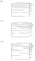
- Fig. 1 is a sectional view illustrating an LED according to an embodiment of the present invention.
- an N-type semiconductor layer 25 is positioned on a substrate 21.
- a buffer layer 23 is interposed between the substrate 21 and the N-type semiconductor layer 25, wherein the buffer layer comprises a low-temperature buffer layer and a high-temperature buffer layer.
- the substrate 21 is not limited particularly but may be, for example, a sapphire, spinel or silicon carbide substrate.
- the N-type semiconductor layer 25 may include an electron injection layer and an N-type clad layer.
- the N-type semiconductor layer may be formed of (Al, Ga, In)N-based Group III nitride semiconductor layer.
- the N-type semiconductor layer 25 may be formed of GaN and/or AlInGaN.
- the N-type semiconductor layer 25 may be doped with an N-type impurity, e.g., Si.
- a P-type semiconductor layer 35 is positioned above the N-type semiconductor layer 25, and an active layer 27 is interposed between the N-type and P-type semiconductor layers 25 and 35.
- the active layer 27 may be formed to have a single quantum well structure or a multiple quantum well structure in which well layers and barrier layers are alternately laminated.
- the well layer may be formed of InGaN, and the barrier layer may be formed of (Al, In, Ga)N.
- the well layer contains In more than the barrier layer, thereby forming a quantum well.
- the P-type semiconductor layer 35 comprises a P-type clad layer 29, a hole injection layer 31 and a P-type contact layer 33.
- the bandgap of the P-type clad layer 29 is wider than that of the hole injection layer 31, and the bandgap of the hole injection layer 31 is equal to that of the P-type contact layer 33. Since the P-type contact layer 33 and the hole injection layer 31 has the same bandgap, a current introduced from an electrode (not shown) may be diffused in the P-type contact layer 33 and then flow into the hole injection layer 31 1 without energy barriers.
- the P-type clad layer 29 is formed of a semiconductor having a wide bandgap so that electrons are restricted in the active layer 27. In addition, since the P-type clad layer 29 has a bandgap relatively wider than the hole injection layer 31, the P-type clad layer 29 helps current to be diffused in the hole injection layer 31.
- a doping concentration of the hole injection layer 31 may be lower than that of the P-type clad layer 29, and a doping concentration of the P-type contact layer 33 may be higher than that of the P-type clad layer 29.
- the P-type contact layer 33 is a layer which is in contact with a conductive electrode (not shown) made of indium tin oxide (ITO) or a metallic material, and is highly doped with impurities to lower contact resistance between the conductive electrode and the P-type contact layer 33.
- the hole injection layer 31 is a layer that produces holes to be injected into the active layer 27. If a doping concentration of the hole injection layer 31 is high, the mobility of holes is decreased in the hole injection layer 31.
- the hole injection layer 31 is formed to have a doping concentration lower than the P-type contact layer 33, thereby improving the mobility of holes.
- the P-type clad layer 29 is also formed to have a doping concentration lower than the P-type contact layer 33 so that holes move smoothly.
- holes produced from the hole injection layer 31 are injected into the active layer 27 via the P-type clad layer 29.
- the doping concentration of the P-type clad layer 29 be relatively higher than that of the hole injection layer 31, the movement of holes from the hole injection layer 31 to the P-type clad layer 29 can be promoted.
- the thickness of the hole injection layer 31 may be larger than that of the P-type clad layer 29, and the thickness of the P-type contact layer 33 may be smaller than that of the P-type clad layer 29.
- the P-type contact layer 33 is formed to be thin, so that it is possible to reduce influence on the mobility of holes and to prevent a forward voltage from being increased.
- the P-type clad layer 29 is formed to be relatively thick, a forward voltage is increased by interrupting the injection of holes, and thus, the recombination rate of electrons and holes is lowered. Therefore, the P-type clad layer 29 is formed to be relatively thinner than the hole injection layer 31, so that the injection of holes can be enhanced.
- the P-type clad layer 29 may be formed of Al x In y Ga 1-x-y N (0 ⁇ x ⁇ 1, 0 ⁇ y ⁇ 1, x+y ⁇ 1).
- the hole injection layer 31 and the P-type contact layer 33 may be formed of GaN. These layers may be formed in-situ by an MOCVD technique, wherein for example, Mg may be used as a P-type impurity.
- Fig. 2 is a sectional view illustrating an LED according to another embodiment of the present invention.
- the LED according to this embodiment has the generally same structure as the LED described with reference to Fig. 1 except that a P-type semiconductor layer 45 further includes an undoped layer 28 interposed between an active layer 27 and a P-type clad layer 29.
- the undoped layer 28 may be formed of the same series semiconductor as the P-type clad layer 29, but is not artificially doped with an impurity.
- the undoped layer 28 may be formed of undoped Al x In y Ga 1-x-y N (0 ⁇ x ⁇ 1, 0 ⁇ y ⁇ 1, x+y ⁇ 1), the undoped layer 28 need not be completely equal to that of the P-type clad layer 29, and the undoped layer 28 may be slightly different from the P-type clad layer 29 in composition ratio.
- the undoped layer 28 prevents an impurity, with which the P-type clad layer 29 is doped, e.g., Mg, from being diffused into the active layer 27. Accordingly, it is possible to prevent non-light emitting recombination from being generated by the impurity diffused into the active layer, thereby enhancing luminous efficiency.
- Fig. 3 is a sectional view illustrating an LED according to a further embodiment of the present invention.
- the LED according to this embodiment has the generally same structure as the LED described with reference to Fig. 2 except that a P-type semiconductor layer 55 further includes a lower undoped layer 30 interposed between a P-type clad layer 29 and a hole injection layer 31 and/or an upper undoped layer 32 interposed between the hole injection layer 31 and a P-type contact layer 33.
- the lower and upper undoped layers 30 and 32 may be formed of the same semiconductor as the hole injection layer 31 without artificial doping.
- lower and upper undoped layers 30 and 32 may be formed of undoped GaN.
- the lower undoped layer 30 may be grown by growing the P-type clad layer 29 of AlInGaN in a chamber and then interrupting inflow of a source gas containing Al and In.
- An undoped layer 28 prevents hydrogen of NH 3 from being combined with impurities in the P-type clad layer 29 while being grown, and also prevents hydrogen being combined with impurities in the P-type clad layer 29 in a process of introducing the NH 3 before the hole injection layer 31 is formed by an in-situ process. Accordingly, Mg in the P-type clad layer 29 can be increasingly activated.
- the upper undoped layer 30 prevents hydrogen from being combined with impurities in the hole injection layer 31, thereby helping activation of impurities in the hole injection layer 31.
- the undoped layer 28 is interposed between the active layer 27 and the P-type clad layer 29 in Fig. 3 .
- the undoped layer 28 and the lower and upper undoped layers 30 and 32 may not be necessarily used together.
- the undoped layer 28 may be omitted.
- electrons are restricted in an active layer by improving a structure of a P-type semiconductor layer and the recombination rate of electrons and holes is enhanced by injecting holes into the active layer smoothly, whereby internal quantum efficiency can be improved. Further, non-light emitting recombination is prevented by preventing impurities from being diffused into the active layer from the P-type semiconductor layer, so that luminous efficiency can be enhanced. Furthermore, undoped GaN is formed between the P-type clad layer and a hole injection layer and/or between the hole injection layer and a P-type contact layer to prevent Mg from being combined with hydrogen and to help Mg to be activated, thereby improving the production and injection of holes.
Landscapes
- Led Devices (AREA)
Applications Claiming Priority (1)
| Application Number | Priority Date | Filing Date | Title |
|---|---|---|---|
| KR1020070072629A KR100838196B1 (ko) | 2007-07-20 | 2007-07-20 | 개선된 구조를 갖는 발광 다이오드 |
Publications (3)
| Publication Number | Publication Date |
|---|---|
| EP2017900A2 true EP2017900A2 (de) | 2009-01-21 |
| EP2017900A3 EP2017900A3 (de) | 2010-05-05 |
| EP2017900B1 EP2017900B1 (de) | 2017-05-17 |
Family
ID=39771297
Family Applications (1)
| Application Number | Title | Priority Date | Filing Date |
|---|---|---|---|
| EP08011718.7A Not-in-force EP2017900B1 (de) | 2007-07-20 | 2008-06-27 | Leuchtdiode mit verbesserter Struktur |
Country Status (3)
| Country | Link |
|---|---|
| US (1) | US8525220B2 (de) |
| EP (1) | EP2017900B1 (de) |
| KR (1) | KR100838196B1 (de) |
Cited By (2)
| Publication number | Priority date | Publication date | Assignee | Title |
|---|---|---|---|---|
| US20120153259A1 (en) * | 2007-09-10 | 2012-06-21 | Seoul Opto Device Co., Ltd. | Light emitting diode with improved structure |
| KR20140137208A (ko) * | 2013-05-22 | 2014-12-02 | 서울바이오시스 주식회사 | 발광 소자 및 그것을 제조하는 방법 |
Families Citing this family (8)
| Publication number | Priority date | Publication date | Assignee | Title |
|---|---|---|---|---|
| JP2013038394A (ja) * | 2011-07-14 | 2013-02-21 | Rohm Co Ltd | 半導体レーザ素子 |
| KR102359845B1 (ko) | 2014-08-19 | 2022-02-09 | 서울바이오시스 주식회사 | 발광 소자 및 그것을 제조하는 방법 |
| DE102015113670B4 (de) * | 2014-08-19 | 2025-12-31 | Seoul Viosys Co., Ltd | Leuchtvorrichtung und Verfahren zu deren Herstellung |
| KR102264671B1 (ko) | 2014-09-30 | 2021-06-15 | 서울바이오시스 주식회사 | 자외선 발광소자 |
| US9966501B2 (en) * | 2015-09-07 | 2018-05-08 | Seoul Viosys Co., Ltd. | Light emitting device with high efficiency |
| US11195975B2 (en) * | 2018-06-12 | 2021-12-07 | Ostendo Technologies, Inc. | Device and method for III-V light emitting micropixel array device having hydrogen diffusion barrier layer |
| CN110635007B (zh) * | 2019-09-12 | 2024-09-27 | 佛山市国星半导体技术有限公司 | 一种抗静电外延结构及其制备方法 |
| CN114300402A (zh) * | 2020-09-30 | 2022-04-08 | 广东晶相光电科技有限公司 | 一种发光二极管及其应用 |
Family Cites Families (8)
| Publication number | Priority date | Publication date | Assignee | Title |
|---|---|---|---|---|
| US6057565A (en) | 1996-09-26 | 2000-05-02 | Kabushiki Kaisha Toshiba | Semiconductor light emitting device including a non-stoichiometric compound layer and manufacturing method thereof |
| JP3864735B2 (ja) * | 2000-12-28 | 2007-01-10 | ソニー株式会社 | 半導体発光素子およびその製造方法 |
| US7692182B2 (en) * | 2001-05-30 | 2010-04-06 | Cree, Inc. | Group III nitride based quantum well light emitting device structures with an indium containing capping structure |
| US6927412B2 (en) * | 2002-11-21 | 2005-08-09 | Ricoh Company, Ltd. | Semiconductor light emitter |
| JP2006108585A (ja) * | 2004-10-08 | 2006-04-20 | Toyoda Gosei Co Ltd | Iii族窒化物系化合物半導体発光素子 |
| US7368759B2 (en) | 2005-09-30 | 2008-05-06 | Hitachi Cable, Ltd. | Semiconductor light-emitting device |
| US7569866B2 (en) * | 2005-09-30 | 2009-08-04 | Hitachi Cable, Ltd. | Semiconductor light-emitting device |
| US7462884B2 (en) | 2005-10-31 | 2008-12-09 | Nichia Corporation | Nitride semiconductor device |
-
2007
- 2007-07-20 KR KR1020070072629A patent/KR100838196B1/ko active Active
-
2008
- 2008-06-23 US US12/143,963 patent/US8525220B2/en active Active
- 2008-06-27 EP EP08011718.7A patent/EP2017900B1/de not_active Not-in-force
Non-Patent Citations (1)
| Title |
|---|
| None |
Cited By (5)
| Publication number | Priority date | Publication date | Assignee | Title |
|---|---|---|---|---|
| US20120153259A1 (en) * | 2007-09-10 | 2012-06-21 | Seoul Opto Device Co., Ltd. | Light emitting diode with improved structure |
| US8575594B2 (en) * | 2007-09-10 | 2013-11-05 | Seoul Opto Device Co., Ltd. | Light emitting diode having a barrier layer with a superlattice structure |
| KR20140137208A (ko) * | 2013-05-22 | 2014-12-02 | 서울바이오시스 주식회사 | 발광 소자 및 그것을 제조하는 방법 |
| EP3001465A4 (de) * | 2013-05-22 | 2017-01-04 | Seoul Viosys Co., Ltd. | Lichtemittierendes element und verfahren zur herstellung davon |
| CN110246938A (zh) * | 2013-05-22 | 2019-09-17 | 首尔伟傲世有限公司 | 发光器件 |
Also Published As
| Publication number | Publication date |
|---|---|
| EP2017900B1 (de) | 2017-05-17 |
| EP2017900A3 (de) | 2010-05-05 |
| KR100838196B1 (ko) | 2008-06-13 |
| US20090020780A1 (en) | 2009-01-22 |
| US8525220B2 (en) | 2013-09-03 |
Similar Documents
| Publication | Publication Date | Title |
|---|---|---|
| EP2017900B1 (de) | Leuchtdiode mit verbesserter Struktur | |
| JP5542226B2 (ja) | 多重量子ウェル構造の活性領域を有する発光ダイオード | |
| US6720570B2 (en) | Gallium nitride-based semiconductor light emitting device | |
| KR100998540B1 (ko) | Iii족 질화물계 반도체 발광 소자 | |
| TWI451591B (zh) | 以氮化物為主之發光裝置 | |
| KR102191213B1 (ko) | 자외선 발광 소자 | |
| JP6587673B2 (ja) | 発光素子 | |
| KR20050021237A (ko) | 발광 소자 및 그 제조 방법 | |
| WO2019015217A1 (zh) | 一种深紫外led | |
| CN112366256B (zh) | 发光二极管外延片及其制造方法 | |
| CN110957401B (zh) | 一种发光二极管及其制作方法 | |
| KR20130102210A (ko) | 질화물 반도체 발광소자 및 그 제조방법 | |
| KR100616516B1 (ko) | 질화갈륨계 반도체 발광소자 및 그 제조방법 | |
| CN108470808A (zh) | 一种发光二极管外延片及其制造方法 | |
| KR100835095B1 (ko) | 질화물 반도체 발광소자 | |
| KR100770440B1 (ko) | 질화물 반도체 발광소자 | |
| KR20100024154A (ko) | 발광 다이오드 | |
| CN112768576B (zh) | 一种发光二极管及制备方法 | |
| KR20130015112A (ko) | 발광 다이오드 및 그것을 제조하는 방법 | |
| KR101876576B1 (ko) | 질화물 반도체 발광소자 및 그 제조방법 | |
| KR100337197B1 (ko) | 질화물 반도체 발광소자 | |
| CN207381424U (zh) | 一种深紫外led | |
| KR102817111B1 (ko) | 디스플레이용 반도체 광원 및 그 제조 방법 | |
| KR100722818B1 (ko) | 발광 다이오드의 제조 방법 | |
| KR101922934B1 (ko) | 질화물 반도체 발광소자 |
Legal Events
| Date | Code | Title | Description |
|---|---|---|---|
| PUAI | Public reference made under article 153(3) epc to a published international application that has entered the european phase |
Free format text: ORIGINAL CODE: 0009012 |
|
| AK | Designated contracting states |
Kind code of ref document: A2 Designated state(s): AT BE BG CH CY CZ DE DK EE ES FI FR GB GR HR HU IE IS IT LI LT LU LV MC MT NL NO PL PT RO SE SI SK TR |
|
| AX | Request for extension of the european patent |
Extension state: AL BA MK RS |
|
| PUAL | Search report despatched |
Free format text: ORIGINAL CODE: 0009013 |
|
| AK | Designated contracting states |
Kind code of ref document: A3 Designated state(s): AT BE BG CH CY CZ DE DK EE ES FI FR GB GR HR HU IE IS IT LI LT LU LV MC MT NL NO PL PT RO SE SI SK TR |
|
| AX | Request for extension of the european patent |
Extension state: AL BA MK RS |
|
| RIC1 | Information provided on ipc code assigned before grant |
Ipc: H01L 33/32 20100101ALN20100329BHEP Ipc: H01L 33/14 20100101AFI20100329BHEP |
|
| 17P | Request for examination filed |
Effective date: 20101105 |
|
| AKX | Designation fees paid |
Designated state(s): AT BE BG CH CY CZ DE DK EE ES FI FR GB GR HR HU IE IS IT LI LT LU LV MC MT NL NO PL PT RO SE SI SK TR |
|
| 17Q | First examination report despatched |
Effective date: 20121221 |
|
| RAP1 | Party data changed (applicant data changed or rights of an application transferred) |
Owner name: SEOUL VIOSYS CO., LTD |
|
| GRAP | Despatch of communication of intention to grant a patent |
Free format text: ORIGINAL CODE: EPIDOSNIGR1 |
|
| STAA | Information on the status of an ep patent application or granted ep patent |
Free format text: STATUS: GRANT OF PATENT IS INTENDED |
|
| RIC1 | Information provided on ipc code assigned before grant |
Ipc: H01L 33/14 20100101AFI20161103BHEP Ipc: H01L 33/32 20100101ALN20161103BHEP |
|
| INTG | Intention to grant announced |
Effective date: 20161206 |
|
| GRAS | Grant fee paid |
Free format text: ORIGINAL CODE: EPIDOSNIGR3 |
|
| GRAA | (expected) grant |
Free format text: ORIGINAL CODE: 0009210 |
|
| STAA | Information on the status of an ep patent application or granted ep patent |
Free format text: STATUS: THE PATENT HAS BEEN GRANTED |
|
| AK | Designated contracting states |
Kind code of ref document: B1 Designated state(s): AT BE BG CH CY CZ DE DK EE ES FI FR GB GR HR HU IE IS IT LI LT LU LV MC MT NL NO PL PT RO SE SI SK TR |
|
| REG | Reference to a national code |
Ref country code: GB Ref legal event code: FG4D |
|
| REG | Reference to a national code |
Ref country code: CH Ref legal event code: EP |
|
| REG | Reference to a national code |
Ref country code: IE Ref legal event code: FG4D |
|
| REG | Reference to a national code |
Ref country code: AT Ref legal event code: REF Ref document number: 895181 Country of ref document: AT Kind code of ref document: T Effective date: 20170615 |
|
| REG | Reference to a national code |
Ref country code: DE Ref legal event code: R096 Ref document number: 602008050292 Country of ref document: DE |
|
| REG | Reference to a national code |
Ref country code: NL Ref legal event code: MP Effective date: 20170517 |
|
| REG | Reference to a national code |
Ref country code: LT Ref legal event code: MG4D |
|
| REG | Reference to a national code |
Ref country code: AT Ref legal event code: MK05 Ref document number: 895181 Country of ref document: AT Kind code of ref document: T Effective date: 20170517 |
|
| PG25 | Lapsed in a contracting state [announced via postgrant information from national office to epo] |
Ref country code: FI Free format text: LAPSE BECAUSE OF FAILURE TO SUBMIT A TRANSLATION OF THE DESCRIPTION OR TO PAY THE FEE WITHIN THE PRESCRIBED TIME-LIMIT Effective date: 20170517 Ref country code: ES Free format text: LAPSE BECAUSE OF FAILURE TO SUBMIT A TRANSLATION OF THE DESCRIPTION OR TO PAY THE FEE WITHIN THE PRESCRIBED TIME-LIMIT Effective date: 20170517 Ref country code: AT Free format text: LAPSE BECAUSE OF FAILURE TO SUBMIT A TRANSLATION OF THE DESCRIPTION OR TO PAY THE FEE WITHIN THE PRESCRIBED TIME-LIMIT Effective date: 20170517 Ref country code: LT Free format text: LAPSE BECAUSE OF FAILURE TO SUBMIT A TRANSLATION OF THE DESCRIPTION OR TO PAY THE FEE WITHIN THE PRESCRIBED TIME-LIMIT Effective date: 20170517 Ref country code: NO Free format text: LAPSE BECAUSE OF FAILURE TO SUBMIT A TRANSLATION OF THE DESCRIPTION OR TO PAY THE FEE WITHIN THE PRESCRIBED TIME-LIMIT Effective date: 20170817 Ref country code: GR Free format text: LAPSE BECAUSE OF FAILURE TO SUBMIT A TRANSLATION OF THE DESCRIPTION OR TO PAY THE FEE WITHIN THE PRESCRIBED TIME-LIMIT Effective date: 20170818 Ref country code: HR Free format text: LAPSE BECAUSE OF FAILURE TO SUBMIT A TRANSLATION OF THE DESCRIPTION OR TO PAY THE FEE WITHIN THE PRESCRIBED TIME-LIMIT Effective date: 20170517 |
|
| PG25 | Lapsed in a contracting state [announced via postgrant information from national office to epo] |
Ref country code: SE Free format text: LAPSE BECAUSE OF FAILURE TO SUBMIT A TRANSLATION OF THE DESCRIPTION OR TO PAY THE FEE WITHIN THE PRESCRIBED TIME-LIMIT Effective date: 20170517 Ref country code: NL Free format text: LAPSE BECAUSE OF FAILURE TO SUBMIT A TRANSLATION OF THE DESCRIPTION OR TO PAY THE FEE WITHIN THE PRESCRIBED TIME-LIMIT Effective date: 20170517 Ref country code: LV Free format text: LAPSE BECAUSE OF FAILURE TO SUBMIT A TRANSLATION OF THE DESCRIPTION OR TO PAY THE FEE WITHIN THE PRESCRIBED TIME-LIMIT Effective date: 20170517 Ref country code: BG Free format text: LAPSE BECAUSE OF FAILURE TO SUBMIT A TRANSLATION OF THE DESCRIPTION OR TO PAY THE FEE WITHIN THE PRESCRIBED TIME-LIMIT Effective date: 20170817 Ref country code: IS Free format text: LAPSE BECAUSE OF FAILURE TO SUBMIT A TRANSLATION OF THE DESCRIPTION OR TO PAY THE FEE WITHIN THE PRESCRIBED TIME-LIMIT Effective date: 20170917 Ref country code: PL Free format text: LAPSE BECAUSE OF FAILURE TO SUBMIT A TRANSLATION OF THE DESCRIPTION OR TO PAY THE FEE WITHIN THE PRESCRIBED TIME-LIMIT Effective date: 20170517 |
|
| PG25 | Lapsed in a contracting state [announced via postgrant information from national office to epo] |
Ref country code: RO Free format text: LAPSE BECAUSE OF FAILURE TO SUBMIT A TRANSLATION OF THE DESCRIPTION OR TO PAY THE FEE WITHIN THE PRESCRIBED TIME-LIMIT Effective date: 20170517 Ref country code: DK Free format text: LAPSE BECAUSE OF FAILURE TO SUBMIT A TRANSLATION OF THE DESCRIPTION OR TO PAY THE FEE WITHIN THE PRESCRIBED TIME-LIMIT Effective date: 20170517 Ref country code: EE Free format text: LAPSE BECAUSE OF FAILURE TO SUBMIT A TRANSLATION OF THE DESCRIPTION OR TO PAY THE FEE WITHIN THE PRESCRIBED TIME-LIMIT Effective date: 20170517 Ref country code: CZ Free format text: LAPSE BECAUSE OF FAILURE TO SUBMIT A TRANSLATION OF THE DESCRIPTION OR TO PAY THE FEE WITHIN THE PRESCRIBED TIME-LIMIT Effective date: 20170517 Ref country code: SK Free format text: LAPSE BECAUSE OF FAILURE TO SUBMIT A TRANSLATION OF THE DESCRIPTION OR TO PAY THE FEE WITHIN THE PRESCRIBED TIME-LIMIT Effective date: 20170517 |
|
| REG | Reference to a national code |
Ref country code: CH Ref legal event code: PL |
|
| REG | Reference to a national code |
Ref country code: DE Ref legal event code: R097 Ref document number: 602008050292 Country of ref document: DE |
|
| PG25 | Lapsed in a contracting state [announced via postgrant information from national office to epo] |
Ref country code: IT Free format text: LAPSE BECAUSE OF FAILURE TO SUBMIT A TRANSLATION OF THE DESCRIPTION OR TO PAY THE FEE WITHIN THE PRESCRIBED TIME-LIMIT Effective date: 20170517 |
|
| PLBE | No opposition filed within time limit |
Free format text: ORIGINAL CODE: 0009261 |
|
| STAA | Information on the status of an ep patent application or granted ep patent |
Free format text: STATUS: NO OPPOSITION FILED WITHIN TIME LIMIT |
|
| REG | Reference to a national code |
Ref country code: FR Ref legal event code: ST Effective date: 20180228 |
|
| REG | Reference to a national code |
Ref country code: IE Ref legal event code: MM4A |
|
| 26N | No opposition filed |
Effective date: 20180220 |
|
| GBPC | Gb: european patent ceased through non-payment of renewal fee |
Effective date: 20170817 |
|
| PG25 | Lapsed in a contracting state [announced via postgrant information from national office to epo] |
Ref country code: CH Free format text: LAPSE BECAUSE OF NON-PAYMENT OF DUE FEES Effective date: 20170630 Ref country code: LI Free format text: LAPSE BECAUSE OF NON-PAYMENT OF DUE FEES Effective date: 20170630 Ref country code: IE Free format text: LAPSE BECAUSE OF NON-PAYMENT OF DUE FEES Effective date: 20170627 Ref country code: LU Free format text: LAPSE BECAUSE OF NON-PAYMENT OF DUE FEES Effective date: 20170627 |
|
| PG25 | Lapsed in a contracting state [announced via postgrant information from national office to epo] |
Ref country code: FR Free format text: LAPSE BECAUSE OF NON-PAYMENT OF DUE FEES Effective date: 20170717 Ref country code: SI Free format text: LAPSE BECAUSE OF FAILURE TO SUBMIT A TRANSLATION OF THE DESCRIPTION OR TO PAY THE FEE WITHIN THE PRESCRIBED TIME-LIMIT Effective date: 20170517 |
|
| REG | Reference to a national code |
Ref country code: BE Ref legal event code: MM Effective date: 20170630 |
|
| PG25 | Lapsed in a contracting state [announced via postgrant information from national office to epo] |
Ref country code: GB Free format text: LAPSE BECAUSE OF NON-PAYMENT OF DUE FEES Effective date: 20170817 |
|
| PG25 | Lapsed in a contracting state [announced via postgrant information from national office to epo] |
Ref country code: BE Free format text: LAPSE BECAUSE OF NON-PAYMENT OF DUE FEES Effective date: 20170630 |
|
| PG25 | Lapsed in a contracting state [announced via postgrant information from national office to epo] |
Ref country code: MT Free format text: LAPSE BECAUSE OF NON-PAYMENT OF DUE FEES Effective date: 20170627 |
|
| PG25 | Lapsed in a contracting state [announced via postgrant information from national office to epo] |
Ref country code: HU Free format text: LAPSE BECAUSE OF FAILURE TO SUBMIT A TRANSLATION OF THE DESCRIPTION OR TO PAY THE FEE WITHIN THE PRESCRIBED TIME-LIMIT; INVALID AB INITIO Effective date: 20080627 Ref country code: MC Free format text: LAPSE BECAUSE OF FAILURE TO SUBMIT A TRANSLATION OF THE DESCRIPTION OR TO PAY THE FEE WITHIN THE PRESCRIBED TIME-LIMIT Effective date: 20170517 |
|
| PG25 | Lapsed in a contracting state [announced via postgrant information from national office to epo] |
Ref country code: CY Free format text: LAPSE BECAUSE OF NON-PAYMENT OF DUE FEES Effective date: 20170517 |
|
| PG25 | Lapsed in a contracting state [announced via postgrant information from national office to epo] |
Ref country code: TR Free format text: LAPSE BECAUSE OF FAILURE TO SUBMIT A TRANSLATION OF THE DESCRIPTION OR TO PAY THE FEE WITHIN THE PRESCRIBED TIME-LIMIT Effective date: 20170517 |
|
| PG25 | Lapsed in a contracting state [announced via postgrant information from national office to epo] |
Ref country code: PT Free format text: LAPSE BECAUSE OF FAILURE TO SUBMIT A TRANSLATION OF THE DESCRIPTION OR TO PAY THE FEE WITHIN THE PRESCRIBED TIME-LIMIT Effective date: 20170517 |
|
| PGFP | Annual fee paid to national office [announced via postgrant information from national office to epo] |
Ref country code: DE Payment date: 20220308 Year of fee payment: 15 |
|
| REG | Reference to a national code |
Ref country code: DE Ref legal event code: R119 Ref document number: 602008050292 Country of ref document: DE |
|
| PG25 | Lapsed in a contracting state [announced via postgrant information from national office to epo] |
Ref country code: DE Free format text: LAPSE BECAUSE OF NON-PAYMENT OF DUE FEES Effective date: 20240103 |