EP2017881A2 - Method of manufacturing semiconductor active layer, method of manufacturing thin film transistor using the same and thin film transistor having semiconductor active layer. - Google Patents
Method of manufacturing semiconductor active layer, method of manufacturing thin film transistor using the same and thin film transistor having semiconductor active layer. Download PDFInfo
- Publication number
- EP2017881A2 EP2017881A2 EP08160476A EP08160476A EP2017881A2 EP 2017881 A2 EP2017881 A2 EP 2017881A2 EP 08160476 A EP08160476 A EP 08160476A EP 08160476 A EP08160476 A EP 08160476A EP 2017881 A2 EP2017881 A2 EP 2017881A2
- Authority
- EP
- European Patent Office
- Prior art keywords
- target
- atomic
- active layer
- igzo
- thin film
- Prior art date
- Legal status (The legal status is an assumption and is not a legal conclusion. Google has not performed a legal analysis and makes no representation as to the accuracy of the status listed.)
- Granted
Links
- 238000004519 manufacturing process Methods 0.000 title claims abstract description 27
- 239000010409 thin film Substances 0.000 title claims description 46
- 239000004065 semiconductor Substances 0.000 title description 29
- 229910052738 indium Inorganic materials 0.000 claims abstract description 44
- 229910052725 zinc Inorganic materials 0.000 claims abstract description 39
- 229910052733 gallium Inorganic materials 0.000 claims abstract description 33
- 150000002500 ions Chemical class 0.000 claims abstract description 25
- 238000000151 deposition Methods 0.000 claims abstract description 19
- 239000000203 mixture Substances 0.000 claims abstract description 12
- 230000008021 deposition Effects 0.000 claims abstract description 10
- 239000011701 zinc Substances 0.000 claims description 53
- 239000000758 substrate Substances 0.000 claims description 24
- XLOMVQKBTHCTTD-UHFFFAOYSA-N Zinc monoxide Chemical compound [Zn]=O XLOMVQKBTHCTTD-UHFFFAOYSA-N 0.000 claims description 19
- 238000000034 method Methods 0.000 claims description 18
- 239000012212 insulator Substances 0.000 claims description 12
- 239000011787 zinc oxide Substances 0.000 claims description 12
- APFVFJFRJDLVQX-UHFFFAOYSA-N indium atom Chemical compound [In] APFVFJFRJDLVQX-UHFFFAOYSA-N 0.000 claims description 8
- GYHNNYVSQQEPJS-UHFFFAOYSA-N Gallium Chemical compound [Ga] GYHNNYVSQQEPJS-UHFFFAOYSA-N 0.000 claims description 6
- YVTHLONGBIQYBO-UHFFFAOYSA-N zinc indium(3+) oxygen(2-) Chemical compound [O--].[Zn++].[In+3] YVTHLONGBIQYBO-UHFFFAOYSA-N 0.000 claims description 3
- 239000010410 layer Substances 0.000 description 125
- 150000001768 cations Chemical class 0.000 description 15
- XKRFYHLGVUSROY-UHFFFAOYSA-N Argon Chemical compound [Ar] XKRFYHLGVUSROY-UHFFFAOYSA-N 0.000 description 10
- YBJHBAHKTGYVGT-ZKWXMUAHSA-N (+)-Biotin Chemical compound N1C(=O)N[C@@H]2[C@H](CCCCC(=O)O)SC[C@@H]21 YBJHBAHKTGYVGT-ZKWXMUAHSA-N 0.000 description 9
- 239000007789 gas Substances 0.000 description 9
- 230000014509 gene expression Effects 0.000 description 9
- FEPMHVLSLDOMQC-UHFFFAOYSA-N virginiamycin-S1 Natural products CC1OC(=O)C(C=2C=CC=CC=2)NC(=O)C2CC(=O)CCN2C(=O)C(CC=2C=CC=CC=2)N(C)C(=O)C2CCCN2C(=O)C(CC)NC(=O)C1NC(=O)C1=NC=CC=C1O FEPMHVLSLDOMQC-UHFFFAOYSA-N 0.000 description 9
- QVGXLLKOCUKJST-UHFFFAOYSA-N atomic oxygen Chemical compound [O] QVGXLLKOCUKJST-UHFFFAOYSA-N 0.000 description 7
- 239000001301 oxygen Substances 0.000 description 7
- 229910052760 oxygen Inorganic materials 0.000 description 7
- 230000008569 process Effects 0.000 description 6
- 229910052786 argon Inorganic materials 0.000 description 5
- 230000005669 field effect Effects 0.000 description 5
- 230000005527 interface trap Effects 0.000 description 5
- 239000008186 active pharmaceutical agent Substances 0.000 description 4
- 230000003247 decreasing effect Effects 0.000 description 4
- -1 e.g. Substances 0.000 description 4
- 238000010894 electron beam technology Methods 0.000 description 4
- 238000004544 sputter deposition Methods 0.000 description 4
- HCHKCACWOHOZIP-UHFFFAOYSA-N Zinc Chemical compound [Zn] HCHKCACWOHOZIP-UHFFFAOYSA-N 0.000 description 3
- 229910021417 amorphous silicon Inorganic materials 0.000 description 3
- 229910021420 polycrystalline silicon Inorganic materials 0.000 description 3
- 229920005591 polysilicon Polymers 0.000 description 3
- 229920006395 saturated elastomer Polymers 0.000 description 3
- OFIYHXOOOISSDN-UHFFFAOYSA-N tellanylidenegallium Chemical compound [Te]=[Ga] OFIYHXOOOISSDN-UHFFFAOYSA-N 0.000 description 3
- 238000012546 transfer Methods 0.000 description 3
- VYPSYNLAJGMNEJ-UHFFFAOYSA-N Silicium dioxide Chemical compound O=[Si]=O VYPSYNLAJGMNEJ-UHFFFAOYSA-N 0.000 description 2
- 238000009825 accumulation Methods 0.000 description 2
- 238000013459 approach Methods 0.000 description 2
- 230000015572 biosynthetic process Effects 0.000 description 2
- 239000007772 electrode material Substances 0.000 description 2
- 238000001017 electron-beam sputter deposition Methods 0.000 description 2
- 239000010408 film Substances 0.000 description 2
- 230000006872 improvement Effects 0.000 description 2
- 239000011229 interlayer Substances 0.000 description 2
- 230000001678 irradiating effect Effects 0.000 description 2
- MGRWKWACZDFZJT-UHFFFAOYSA-N molybdenum tungsten Chemical compound [Mo].[W] MGRWKWACZDFZJT-UHFFFAOYSA-N 0.000 description 2
- 238000000623 plasma-assisted chemical vapour deposition Methods 0.000 description 2
- 238000004549 pulsed laser deposition Methods 0.000 description 2
- 229910052814 silicon oxide Inorganic materials 0.000 description 2
- 229910052581 Si3N4 Inorganic materials 0.000 description 1
- 229910004205 SiNX Inorganic materials 0.000 description 1
- 230000002411 adverse Effects 0.000 description 1
- 239000000969 carrier Substances 0.000 description 1
- 239000012159 carrier gas Substances 0.000 description 1
- 230000008859 change Effects 0.000 description 1
- 239000004020 conductor Substances 0.000 description 1
- 230000005516 deep trap Effects 0.000 description 1
- 238000011161 development Methods 0.000 description 1
- 230000018109 developmental process Effects 0.000 description 1
- 230000005684 electric field Effects 0.000 description 1
- 230000005672 electromagnetic field Effects 0.000 description 1
- 239000011521 glass Substances 0.000 description 1
- 238000010348 incorporation Methods 0.000 description 1
- PJXISJQVUVHSOJ-UHFFFAOYSA-N indium(III) oxide Inorganic materials [O-2].[O-2].[O-2].[In+3].[In+3] PJXISJQVUVHSOJ-UHFFFAOYSA-N 0.000 description 1
- 239000011261 inert gas Substances 0.000 description 1
- 230000031700 light absorption Effects 0.000 description 1
- 238000005259 measurement Methods 0.000 description 1
- 238000000059 patterning Methods 0.000 description 1
- 238000005289 physical deposition Methods 0.000 description 1
- 230000004044 response Effects 0.000 description 1
- HQVNEWCFYHHQES-UHFFFAOYSA-N silicon nitride Chemical compound N12[Si]34N5[Si]62N3[Si]51N64 HQVNEWCFYHHQES-UHFFFAOYSA-N 0.000 description 1
- JBQYATWDVHIOAR-UHFFFAOYSA-N tellanylidenegermanium Chemical compound [Te]=[Ge] JBQYATWDVHIOAR-UHFFFAOYSA-N 0.000 description 1
- 229910052721 tungsten Inorganic materials 0.000 description 1
Images


Classifications
-
- C—CHEMISTRY; METALLURGY
- C23—COATING METALLIC MATERIAL; COATING MATERIAL WITH METALLIC MATERIAL; CHEMICAL SURFACE TREATMENT; DIFFUSION TREATMENT OF METALLIC MATERIAL; COATING BY VACUUM EVAPORATION, BY SPUTTERING, BY ION IMPLANTATION OR BY CHEMICAL VAPOUR DEPOSITION, IN GENERAL; INHIBITING CORROSION OF METALLIC MATERIAL OR INCRUSTATION IN GENERAL
- C23C—COATING METALLIC MATERIAL; COATING MATERIAL WITH METALLIC MATERIAL; SURFACE TREATMENT OF METALLIC MATERIAL BY DIFFUSION INTO THE SURFACE, BY CHEMICAL CONVERSION OR SUBSTITUTION; COATING BY VACUUM EVAPORATION, BY SPUTTERING, BY ION IMPLANTATION OR BY CHEMICAL VAPOUR DEPOSITION, IN GENERAL
- C23C14/00—Coating by vacuum evaporation, by sputtering or by ion implantation of the coating forming material
- C23C14/06—Coating by vacuum evaporation, by sputtering or by ion implantation of the coating forming material characterised by the coating material
- C23C14/08—Oxides
- C23C14/086—Oxides of zinc, germanium, cadmium, indium, tin, thallium or bismuth
-
- C—CHEMISTRY; METALLURGY
- C23—COATING METALLIC MATERIAL; COATING MATERIAL WITH METALLIC MATERIAL; CHEMICAL SURFACE TREATMENT; DIFFUSION TREATMENT OF METALLIC MATERIAL; COATING BY VACUUM EVAPORATION, BY SPUTTERING, BY ION IMPLANTATION OR BY CHEMICAL VAPOUR DEPOSITION, IN GENERAL; INHIBITING CORROSION OF METALLIC MATERIAL OR INCRUSTATION IN GENERAL
- C23C—COATING METALLIC MATERIAL; COATING MATERIAL WITH METALLIC MATERIAL; SURFACE TREATMENT OF METALLIC MATERIAL BY DIFFUSION INTO THE SURFACE, BY CHEMICAL CONVERSION OR SUBSTITUTION; COATING BY VACUUM EVAPORATION, BY SPUTTERING, BY ION IMPLANTATION OR BY CHEMICAL VAPOUR DEPOSITION, IN GENERAL
- C23C14/00—Coating by vacuum evaporation, by sputtering or by ion implantation of the coating forming material
- C23C14/22—Coating by vacuum evaporation, by sputtering or by ion implantation of the coating forming material characterised by the process of coating
- C23C14/34—Sputtering
- C23C14/3464—Sputtering using more than one target
-
- H—ELECTRICITY
- H01—ELECTRIC ELEMENTS
- H01L—SEMICONDUCTOR DEVICES NOT COVERED BY CLASS H10
- H01L21/00—Processes or apparatus adapted for the manufacture or treatment of semiconductor or solid state devices or of parts thereof
- H01L21/02—Manufacture or treatment of semiconductor devices or of parts thereof
- H01L21/02104—Forming layers
- H01L21/02365—Forming inorganic semiconducting materials on a substrate
- H01L21/02367—Substrates
- H01L21/0237—Materials
- H01L21/02422—Non-crystalline insulating materials, e.g. glass, polymers
-
- H—ELECTRICITY
- H01—ELECTRIC ELEMENTS
- H01L—SEMICONDUCTOR DEVICES NOT COVERED BY CLASS H10
- H01L21/00—Processes or apparatus adapted for the manufacture or treatment of semiconductor or solid state devices or of parts thereof
- H01L21/02—Manufacture or treatment of semiconductor devices or of parts thereof
- H01L21/02104—Forming layers
- H01L21/02365—Forming inorganic semiconducting materials on a substrate
- H01L21/02518—Deposited layers
- H01L21/02521—Materials
- H01L21/02551—Group 12/16 materials
- H01L21/02554—Oxides
-
- H—ELECTRICITY
- H01—ELECTRIC ELEMENTS
- H01L—SEMICONDUCTOR DEVICES NOT COVERED BY CLASS H10
- H01L21/00—Processes or apparatus adapted for the manufacture or treatment of semiconductor or solid state devices or of parts thereof
- H01L21/02—Manufacture or treatment of semiconductor devices or of parts thereof
- H01L21/02104—Forming layers
- H01L21/02365—Forming inorganic semiconducting materials on a substrate
- H01L21/02518—Deposited layers
- H01L21/02521—Materials
- H01L21/02565—Oxide semiconducting materials not being Group 12/16 materials, e.g. ternary compounds
-
- H—ELECTRICITY
- H01—ELECTRIC ELEMENTS
- H01L—SEMICONDUCTOR DEVICES NOT COVERED BY CLASS H10
- H01L21/00—Processes or apparatus adapted for the manufacture or treatment of semiconductor or solid state devices or of parts thereof
- H01L21/02—Manufacture or treatment of semiconductor devices or of parts thereof
- H01L21/02104—Forming layers
- H01L21/02365—Forming inorganic semiconducting materials on a substrate
- H01L21/02612—Formation types
- H01L21/02617—Deposition types
- H01L21/02631—Physical deposition at reduced pressure, e.g. MBE, sputtering, evaporation
-
- H—ELECTRICITY
- H01—ELECTRIC ELEMENTS
- H01L—SEMICONDUCTOR DEVICES NOT COVERED BY CLASS H10
- H01L29/00—Semiconductor devices adapted for rectifying, amplifying, oscillating or switching, or capacitors or resistors with at least one potential-jump barrier or surface barrier, e.g. PN junction depletion layer or carrier concentration layer; Details of semiconductor bodies or of electrodes thereof ; Multistep manufacturing processes therefor
- H01L29/66—Types of semiconductor device ; Multistep manufacturing processes therefor
- H01L29/68—Types of semiconductor device ; Multistep manufacturing processes therefor controllable by only the electric current supplied, or only the electric potential applied, to an electrode which does not carry the current to be rectified, amplified or switched
- H01L29/76—Unipolar devices, e.g. field effect transistors
- H01L29/772—Field effect transistors
- H01L29/78—Field effect transistors with field effect produced by an insulated gate
- H01L29/786—Thin film transistors, i.e. transistors with a channel being at least partly a thin film
- H01L29/7869—Thin film transistors, i.e. transistors with a channel being at least partly a thin film having a semiconductor body comprising an oxide semiconductor material, e.g. zinc oxide, copper aluminium oxide, cadmium stannate
Definitions
- Embodiments relate to a method of manufacturing a semiconductor active layer, a method of manufacturing a thin film transistor using the same, and a thin film transistor including the semiconductor active layer.
- a semiconductor layer using amorphous silicon or polysilicon has recently been developed for use in a thin film transistor (TFT) for light emitting display devices such as organic light emitting display devices, which use organic light emitting diodes (OLEDs) to emit light.
- TFT thin film transistor
- OLEDs organic light emitting diodes
- the semiconductor layer When the semiconductor layer is formed of amorphous silicon, the semiconductor layer may exhibit low mobility. The use of such a low mobility layer as a drive circuit of a display panel that requires a fast response time may be difficult.
- Polysilicon may be used as the semiconductor layer to provide high mobility, but the threshold voltage of the TFT may not be uniform. Additionally, leakage current may occur in the amorphous silicon or polysilicon semiconductor layer when light, e.g., light from a backlight unit, is incident thereon.
- Oxide-based semiconductors may exhibit a band gap that is higher than the light energy in a visible light region. Accordingly, an oxide-based semiconductor may exhibit little or no leakage current resulting from visible light absorption. Therefore, the use of oxide-based semiconductors, e.g., semiconductors having an indium-gallium-zinc oxide (hereinafter, "IGZO") active layer, has been proposed as a solution to problems in the art. However, there is a need for further developments in the formation of an IGZO active layer, e.g., to provide control over the atomic composition thereof and improve the electrical characteristics of devices including the IGZO active layer.
- IGZO indium-gallium-zinc oxide
- Embodiments are therefore directed to a method of manufacturing a semiconductor active layer, a method of manufacturing a thin film transistor using the same, and a thin film transistor including the semiconductor active layer, which substantially overcome one or more of the problems due to the limitations and disadvantages of the related art.
- At least one of the above and other features and advantages may be realized by providing a method of manufacturing an IGZO active layer, the method including depositing ions including In, Ga, and Zn from a first target, and depositing ions including In from a second target having a different atomic composition from the first target.
- the deposition of ions from the second target may be controlled to adjust an atomic% of In in the IGZO layer to be about 45 atomic% to about 80 atomic%.
- the atomic% of In in the IGZO layer may be about 55 atomic% to about 75 atomic%.
- the atomic% of In in the IGZO layer may be about 60 atomic% to about 70 atomic%.
- the first target may include In, Ga, and Zn in a molar ratio of about 1:1:1.
- the first target may be made of InGaZnO, and the second target is made of InZnO.
- the first target may include In, Ga, and Zn in a molar ratio of about 1:1:1, and the second target may includes In and Zn in a molar ratio of about 1:1 to about 6:1 (In:Zn).
- the atomic% of In in the IGZO layer may be adjusted by adjusting a molar ratio of In:Zn in the second target.
- First and second bias powers may be applied to the first target and the second target, respectively, and the atomic% of In in the IGZO layer may be adjusted by adjusting the intensity of the second bias power.
- the first target and the second target may be irradiated with first and second pulsed lasers, and the atomic% of In in the IGZO layer may be adjusted by adjusting the intensity of the second pulsed laser.
- At least one of the above and other features and advantages may also be realized by providing a method of manufacturing a thin film transistor, the method including forming an IGZO active layer on a substrate, forming a gate electrode spaced apart from the IGZO active layer by a gate dielectric layer, forming a source electrode that contacts a first portion of the IGZO active layer, and forming a drain electrode that contacts a second portion of the IGZO active layer.
- Forming the IGZO active layer may include depositing ions including In, Ga, and Zn from a first target, and depositing ions including In from a second target having a different atomic composition from the first target, the deposition of ions from the second target being controlled to adjust an atomic% of In in the IGZO layer to be about 45 atomic% to about 80 atomic%.
- the atomic% of In in the IGZO layer may be about 55 atomic% to about 75 atomic%.
- the atomic% of In in the IGZO layer may be about 60 atomic% to about 70 atomic%.
- the first target may include In, Ga, and Zn in a molar ratio of about 1:1:1.
- the first target may be made of InGaZnO
- the second target may be made of InZnO.
- the first target may include In, Ga, and Zn in a molar ratio of about 1:1:1, and the second target may include In and Zn in a molar ratio of about 1:1 to about 6:1 (In:Zn).
- the atomic% of In in the IGZO layer may be adjusted by adjusting a molar ratio of In:Zn in the second target.
- First and second bias powers may be applied to the first target and the second target, respectively, and the atomic% of In in the IGZO layer may be adjusted by adjusting the intensity of the second bias power.
- the first target and the second target may be irradiated with first and second pulsed lasers, and the atomic% of In in the IGZO layer may be adjusted by adjusting the intensity of the second pulsed laser.
- the gate dielectric layer may be on the gate electrode such that the gate electrode is between the gate dielectric layer and the substrate, and the IGZO active layer may be on the gate dielectric layer.
- the gate dielectric layer may be on the IGZO active layer such that the IGZO active layer is between the gate dielectric layer and the substrate, and the gate electrode may be on the gate dielectric layer.
- a thin film transistor including a substrate, an IGZO active layer on the substrate, the IGZO layer including a channel region, a source region, and a drain region, a gate electrode overlapping the channel region and insulated from the active layer by a gate insulator, and source and drain electrodes contacting the source and drain regions, respectively.
- An atomic% of In in the IGZO active layer may be about 45 atomic% to about 80 atomic%.
- the atomic% of In in the IGZO active layer may be about 55 atomic% to about 75 atomic%.
- each of the expressions “at least one of A, B, and C,” “at least one of A, B, or C,” “one or more of A, B, and C,” “one or more of A, B, or C” and "A, B, and/or C” includes the following meanings: A alone; B alone; C alone; both A and B together; both A and C together; both B and C together; and all three of A, B, and C together.
- the expression “or” is not an “exclusive or” unless it is used in conjunction with the term “either.”
- the expression “A, B, or C” includes A alone; B alone; C alone; both A and B together; both A and C together; both B and C together; and all three of A, B and, C together
- the expression “either A, B, or C” means one of A alone, B alone, and C alone, and does not mean any of both A and B together; both A and C together; both B and C together; and all three of A, B and C together.
- a gas may represent a single component, e.g., argon, or multiple components in combination, e.g., argon mixed with oxygen.
- atomic ratio and “molar ratio” are synonymous. Additionally, the terms “atomic percentage” and “atomic%” indicate the amount of one of indium (In), gallium (Ga), or zinc (Zn) relative to amount of indium, gallium and zinc combined, unless indicated otherwise.
- Embodiments may provide a method of manufacturing a semiconductor active layer capable of increasing an atomic% of indium (In) in an IGZO semiconductor active layer.
- the mobility of a carrier (electrons) may increase if the relative amount of indium (In) is increased, and a concentration of the carrier (electrons) may decrease if the relative amount of gallium (Ga) is increased.
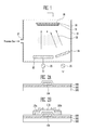
- FIG. 1 illustrates a schematic view of a codeposition apparatus according to an embodiment.
- ions of In, Ga and Zn may be deposited from a first target 22, e.g., a target made of InGaZnO, to form an IGZO layer 31 on a substrate 30, and ions of In may be deposited from a second target 24, e.g., a target made of InZnO, to adjust a compositional ratio of In in the IGZO layer.
- a first target 22 e.g., a target made of InGaZnO
- a target made of InZnO e.g., a target made of InZnO
- two targets 22 and 24, e.g., an InGaZnO target and an InZnO target may be used to suitably control the atomic ratio of cations such as In, Ga and Zn in the active layer. This may provide better control over the compositional ratio of In, Ga and Zn cations in the IGZO layer
- FIG. 1 illustrates a cosputtering apparatus. It will be appreciated that other physical deposition operations, e.g., electron beam sputtering, pulsed laser deposition, etc., may also be used.
- the first target 22 and the second target 24 may be disposed at one side of the inside of a chamber 10 having a gas inlet 12 and a gas outlet (not shown) formed therein.
- a first bias power 23 and a second bias power 25 may be applied to the first target 22 and the second target 24, respectively.
- a plate 26 may support the substrate 30, and may be disposed inside of the chamber 10 to face the first target 22 and the second target 24.
- the plate 26 may be coupled to a grounding conductor. In an implementation, the potential of the plate 26 may be varied depending on whether the first bias power 23 and the second bias power 25 are applied.
- An inert gas, e.g., argon (Ar), and a carrier gas, e.g., oxygen (O 2 ), may be supplied as a process gas into the chamber 10 through the gas inlet 12.
- the amount of oxygen (O 2 ) supplied may be adjusted according to the desired electrical characteristics of the semiconductor active layer.
- a concentration of the carrier may be adjusted by adjusting the partial pressure of oxygen (O 2 ) in the process gas. For example, the concentration of the carrier may be decreased if the partial pressure of oxygen (O 2 ) is increased, and the concentration of the carrier may be increased if the partial pressure of oxygen (O 2 ) is decreased.
- the first bias power 23 and the second bias power 25 may be applied to the InGaZnO target 22 and the InZnO target 24, respectively, while the process gas is supplied.
- An electric field may be formed between the plate 26 and the InGaZnO target 22 and InZnO target 24, and a high density plasma 28 may be generated by the bombardment of process gas molecules with electrons accelerated by an applied electromagnetic field.
- Cations of In, Ga and Zn may be deposited from the InGaZnO target 22, and cations of In and Zn may be deposited from the InZnO target 24 by the plasma 28 using a sputtering operation so as to form the IGZO active layer 31 on the substrate 30.
- the compositional ratio (atomic%) of the cations of In, Ga, and Zn may be controlled according to the respective intensities of the first bias power 23 and the second bias power 25.
- the compositional ratio of In in the IGZO active layer 31 may be adjusted by increasing a speed for deposition of In and Zn ions from the InZnO target 24, e.g., a sputtering rate of the InZnO target 24 may be increased more than that of the InGaZnO target 22 by adjusting the intensity of the second bias power 25.
- the amount of Ga in the IGZO active layer 31 may be set to about 10 atomic% or more. This may reduce or avoid the formation of excess carriers that may lead to unstable electrical characteristics, e.g., an increased OFF current or variations in threshold voltage.
- the compositional ratio (atomic%) of the cations of In, Ga, and Zn may be controlled by adjusting the molar ratios of these elements in the InGaZnO target 22 and/or the InZnO target 24.
- the InGaZnO target 22 preferably consists of an indium gallium zinc oxide composition and the contents of indium, gallium and zinc can be modified.
- the InZnO target 24 preferably consists of an indium zinc oxide composition, wherein the contents of indium and zinc can be modified.
- the molar ratio of In:Ga:Zn in the InGaZnO target 22 may be about 1:1:1, and the compositional ratio of In in the IGZO active layer 31 may be adjusted to about 45 atomic% to about 80 atomic% by increasing the amount of In in the InZnO target 24.
- the molar ratio of In:Zn in the InZnO target 24 may be about 1:1 to about 6:1 (In:Zn).
- the compositional ratio of In in the IGZO active layer may be about 55 atomic% to about 75 atomic%, or about 60 atomic% to about 70 atomic%.
- an electron beam sputtering apparatus may be used. Cations of In, Ga, and Zn may be deposited from the InGaZnO target 22 and the InZnO target 24 by irradiating the InGaZnO target 22 and the InZnO target 24 with first and second electron beams (not shown), thereby forming the IGZO active layer 31 on the substrate 30.
- the compositional ratio of the cations of In, Ga, and Zn in the IGZO active layer 31 may be adjusted according to the intensity of the first and second electron beams and/or the molar ratio of In, Ga, and Zn in the InGaZnO target 22 and the molar ratio of In and Zn in the InZnO target 24.
- a pulsed laser deposition apparatus may be used. Cations of In, Ga, and Zn may be deposited from the InGaZnO target 22 and the InZnO target 24 by irradiating the InGaZnO target 22 and the InZnO target 24 with first and second pulsed lasers (not shown), thereby forming the IGZO active layer 31 on the substrate 30.
- the compositional ratio of the cations of In, Ga, and Zn in the IGZO active layer 31 may be adjusted according to the intensity of the first and second pulsed lasers and/or the molar ratio of In, Ga, and Zn in the InGaZnO target 22 and the molar ratio of In and Zn in the InZnO target 24.
- the IGZO active layer 31 manufactured according to embodiments may have a composition where the cations are spatially non-uniform due to the use of two targets 22, 24.
- the relative ratio of In:Ga:Zn in the IGZO active layer 31 may vary across the substrate 30, i.e., it may vary according to (x, y) coordinates when mapped along X and Y axes that are parallel to the substrate 30. Therefore, the IGZO active layer 31 according to an embodiment may exhibit structural differences from an IGZO layer manufactured using a single target of InGaZnO.
- FIGS. 2A and 2B illustrate cross-sectional views of stages in a method of manufacturing a bottom gate (an inverted staggered bottom gate) thin film transistor according to an embodiment.
- a buffer layer 102 may be formed on a substrate 100, and a gate electrode 104 may be formed on the buffer layer 102.
- a gate insulator 106 may be formed on the buffer layer 102 and on the gate electrode 104.
- an IGZO active layer 108 providing a channel region, a source region and a drain region may be formed on the gate insulator 106.
- the active layer 108 may be formed according to an embodiment, e.g., as described above in connection with FIG. 1 .
- the IGZO active layer may be formed on the substrate 100 by depositing ions, including In, Ga and Zn, from the InGaZnO target 22 and the InZnO target 24.
- the compositional ratio of In may be adjusted to, e.g., about 45 atomic% to about 80 atomic%, e.g., by adjusting the intensity of a bias power, adjusting the intensity of an electron beam or a pulse laser, or adjusting the molar ratios of the components of the InGaZnO target 22 and/or InZnO target 24.
- the IGZO active layer 108 may then be patterned, and source and drain electrodes 110a and 110b may be formed to contact the respective source and drain regions of the IGZO active layer 108.
- a buffer layer was formed as a silicon oxide film (SiO x ) on a glass substrate, and 200 nm-thick tungsten molybdenum (MoW) was deposited thereon and then patterned to form a gate electrode on the buffer layer.
- the lateral dimensions of the gate electrode were 70 mm ⁇ 70 mm.
- a 200 nm-thick silicon nitride film (SiN x ) was deposited at a temperature of 330 °C using a plasma-enhanced chemical vapor deposition (PECVD) operation to form a gate insulator on the buffer layer and on the gate electrode.
- PECVD plasma-enhanced chemical vapor deposition
- An IGZO active layer was formed on the gate insulator in an ambient temperature using a cosputtering apparatus.
- An amorphous phase of the IGZO active layer was formed having a thickness of 50 nm.
- the width and length of the channel region of the active layer were 1000 ⁇ m and 150 ⁇ m, respectively.
- a first target of In 2 Ga 2 ZnO 7 i.e., InGaZnO
- a second target of In 2 O 3 -10wt%ZnO 90 weight% In 2 O 3 and 10 weight% ZnO
- the internal pressure of the process chamber in the cosputtering apparatus was maintained at about 5 mTorr, and argon (Ar) and oxygen (O 2 ) were supplied as the process gas at a ratio of 65:35 (Ar:O 2 ).
- a radiofrequency (RF) bias power of 450 W was applied to the first target of In 2 Ga 2 ZnO 7 , and a RF bias power of from 0 W to 700 W was applied to the second target of In 2 O 3 -10wt%ZnO.
- the IGZO active layer was patterned and a 200 nm-thick transparent electrode material of indium zinc oxide (IZO) was deposited at ambient temperature.
- the electrode material was then patterned to form source and drain electrodes and on the entire upper surface, so that the source and drain electrodes were in contact with the source and drain regions, respectively, of the IGZO active layer.
- a shadow mask was used for the patterning operation, and the thin film transistor thus manufactured was heat-treated at a temperature of 350 °C for 1 hour.
- FIGS. 3A and 3B illustrate graphs showing transfer characteristics of thin film transistors manufactured according to the above-described operations.
- a semiconductor parameter analyzer (Agilent 4156C) was used to analyze electrical characteristics of the example thin film transistors (measurements were carried out at ambient temperature).
- FIG. 3A illustrates the results for a thin film transistor manufactured using a bias power of 0 W applied to the In 2 O 3 -10wt%ZnO target.
- FIG. 3B illustrates the results for a thin film transistor manufactured using a bias power of 400 W applied to the In 2 O 3 -10wt%ZnO target.
- V T,sat For a drain voltage (V DS ) of 5.1V and an electric current of L/W ⁇ 10 nA flowing through the drain electrode, the threshold voltage (V T,sat ) is defined by a voltage applied to the gate electrode.
- ⁇ FE L ⁇ g m W ⁇ C i ⁇ V DS
- Equation 1 C i and g m are gate capacitance and transconductance per unit area, respectively.
- L and w are length and width, respectively.
- a slope factor S (S factor) may be calculated from the transfer characteristics, as shown in the following Equation 2.
- S d ⁇ V GS d log I DS
- I DS is the saturated drain current
- V GS is the voltage between the gate and source.
- N t S ⁇ log e / kT / q - 1 ⁇ C i q
- N-channel conductivity having a mobility ( ⁇ FE ) of 11.2 ⁇ 2.0 cm 2 /Vs was observed in the thin film transistor.
- the slope factor S (S factor) and the ON/OFF current ratio (I on/off ) were 1.11 ⁇ 0.06 V/dec and ⁇ 6.6 ⁇ 10 6 , respectively.
- FIGS. 3C and 3D show the results obtained by measuring output characteristics of the thin film transistor manufactured according to the above-described operations.
- FIG. 3C shows the results for a bias power of 0 W applied to the second target, i.e., the In 2 O 3 -10wt%ZnO target.
- FIG. 3D shows the results for a bias power of 400 W applied to the second target.
- the thin film transistor according to an embodiment showed pinch-off and saturation characteristics as in the case of the field effect transistor (FET).
- FET field effect transistor
- An organic light emitting display apparatus requires a drain current (I DS ) of about 1 ⁇ A to display full white grayscale.
- the thin film transistor When the bias power applied to the second target was 0 W, the thin film transistor had a saturated drain current (I DS ) of about 1.0 ⁇ A when a voltage (V GS ) between the gate and source was 8 V. When the bias power applied to the second target was 400 W, the thin film transistor had a saturated drain current (I DS ) of about 1.0 ⁇ A when a voltage (V GS ) between the gate and source was 1V ⁇ 4V.
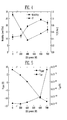
- FIG. 4 illustrates a graph of mobility ( ⁇ FE ) and slope factor S characteristics of the thin film transistor with respect to the bias power applied to the second target, i.e., the In 2 O 3 -10wt%ZnO ("InZnO") target.
- the mobility ( ⁇ FE ) generally increased as the bias power applied to the InZnO target increased.
- the bias power increased up to 600 W
- the mobility increased to 24.0 ⁇ 0.64 cm 2 /Vs.
- the mobility slightly decreased, to 21.7 ⁇ 1.39 cm 2 /Vs when the bias power was 700 W.
- FIG. 5 illustrates a graph of threshold voltage (V T , sat ) and leakage current (OFF current I OFF ) characteristics with respect to the bias power applied to the second target, i.e., the InZnO target.
- the threshold voltage (V T,Sat ) may be controlled according to the bias power applied to the InZnO target.
- the bias power is preferably adjusted to 600 W or less, since leakage current increases rapidly if the bias power is increased up to 700 W or more.
- the threshold voltage (V T,Sat ) slowly decreased.
- the thin film transistor changed from accumulation mode to depletion mode (threshold voltage (V T,sat ) of - 12.1 ⁇ 1.91 V) when the bias power was 700 W.
- the decrease in the mobility ( ⁇ FE ) associated with the high bias power applied to the second target, i.e., the InZnO target, shown in FIG. 4 is due to the bombardment of ions having a high energy during the sputtering operation. Interfacial characteristics with a bottom gate insulator may be deteriorated by the bombardment of strong ions. Also, the generation of deep level defects by the bombardment of ions under the high bias power condition and/or incorporation of sputtering ions such as argon (Ar+) in the thin film may adversely affect the device characteristics. Evidence of such is shown by the changes in the gate voltage and increases in the density of interface trap states (N t ) under the bias power condition of 600 W or more. Table 1, below, provides additional data in this regard.
- Table 1 tabulates the changes in the relative amounts of the cations (In, Ga and Zn) in the IGZO layer and density of interface trap states (N t ) with respect to the bias power applied to the second target, i.e., the InZnO target.
- the data shown in Table 1 reflects the use of the InGaZnO target as the first target and the InZnO target as the second target.
- increases in the bias power applied to the second target resulted in an improved deposition rate and increased relative proportion of In.
- the amount of the In deposited from the InZnO target may be increased by the improved deposition rate.
- Table 1 RF power of IZO target 0 W 300 W 400 W 600 W 700 W In/(In+Ga+Zn) 0.40 0.63 0.65 0.73 0.76 Ga/(In+Ga+Zn) 0.43 0.26 0.23 0.16 0.13 Zn/(In+Ga+Zn) 0.17 0.11 0.12 0.11 0.11 N t (10 12 cm -2 ) 3.2 ⁇ 0.18 1.9 ⁇ 0.06 0.91 ⁇ 0.06 1.5 ⁇ 0.03 1.8 ⁇ 0.27
- the compositional ratio of In the IGZO active layer may be adjusted to be about 45 atomic% to about 80 atomic%.
- the compositional ratio of In is adjusted to be about 55 atomic% to about 75 atomic%, which may optimize mobility and improve the slope factor S.
- the measured characteristics included field-effect mobility ( ⁇ FE ), slope factor S (S), ON/OFF current ratio (I on/off ), threshold voltage (V T,Sat ), and density of interface trap states (N t ).
- ⁇ FE field-effect mobility
- S slope factor S
- I on/off ON/OFF current ratio
- V T,Sat threshold voltage
- N t density of interface trap states
- FIGS. 6A and 6B illustrate cross-sectional views of stages in a method of manufacturing a top gate thin film transistor according to an embodiment.
- a buffer layer 202 may be formed on a substrate 200, and an active layer 204 providing a channel region, a source region and a drain region may be formed on the buffer layer 202.
- the active layer 204 may be formed according to the method of manufacturing a semiconductor active layer shown in FIG. 1 .
- Ions of In, Ga and Zn may be deposited from the InGaZnO target 22 and the InZnO target 24 to form the IGZO active layer 204 on the substrate 200.
- the compositional ratio of In in the IGZO layer may be adjusted to be, e.g., about 45 atomic% to about 80 atomic%.
- the compositional ratio of In in the IGZO active layer 204 may be controlled by, e.g., adjusting the intensity of a bias power, the intensity of an electron beam, the intensity of a pulsed laser, or the molar ratio of In and Zn in the InZnO target 24. Referring to FIG.
- a gate insulator 206 may be formed on the entire surface of the substrate 200, including on the IGZO active layer 204, and a gate electrode 208 may be formed on the gate insulator 206 over the channel region of the active layer 204.
- An interlayer insulator 210 may be formed on the gate electrode 208, and the interlayer insulator 210 and the gate insulator 206 may be patterned to form contact holes so as to expose a predetermined region of the source and drain regions.
- Source and drain electrodes 212a and 212b may be formed to contact the source and drain regions, respectively, of the IGZO active layer 204 through the contact holes.
- embodiments may provide a method of manufacturing a semiconductor active layer capable of controlling a compositional ratio of cations in an IGZO active layer, a method of manufacturing a thin film transistor using the same and a thin film transistor having the semiconductor active layer. Electrical characteristics of the thin film transistor may thus be improved.
- the cations of In, Ga and Zn may be deposited from a first InGaZnO target and a second InZnO target to form the IGZO active layer on the substrate.
- a compositional ratio of In in the IGZO active layer so formed may be about 45 atomic% to 80 atomic%, and may be controlled by increasing a deposition rate of the In and Zn ions from the second InZnO target.
- the electrical characteristics, including mobility and slope factor S, of the thin film transistor may be improved by employing as the active layer the IGZO semiconductor having an increased In content.
- Example embodiments of the present invention have been disclosed herein, and although specific terms are employed, they are used and are to be interpreted in a generic and descriptive sense only and not for purpose of limitation.
- the codeposition approach described herein may employ two targets, as in the examples set forth above, or more than two targets.
- the codeposition approach described herein may be employed to manufacture IGZO layers having atomic compositions other than those described in the examples above, or may be employed to manufacture other oxide or non-oxide layers.
- the above embodiments describe the manufacture of a thin film transistor as a specific example, other semiconductor devices may also be manufactured.
Abstract
Description
- Embodiments relate to a method of manufacturing a semiconductor active layer, a method of manufacturing a thin film transistor using the same, and a thin film transistor including the semiconductor active layer.
- A semiconductor layer using amorphous silicon or polysilicon has recently been developed for use in a thin film transistor (TFT) for light emitting display devices such as organic light emitting display devices, which use organic light emitting diodes (OLEDs) to emit light.
- When the semiconductor layer is formed of amorphous silicon, the semiconductor layer may exhibit low mobility. The use of such a low mobility layer as a drive circuit of a display panel that requires a fast response time may be difficult. Polysilicon may be used as the semiconductor layer to provide high mobility, but the threshold voltage of the TFT may not be uniform. Additionally, leakage current may occur in the amorphous silicon or polysilicon semiconductor layer when light, e.g., light from a backlight unit, is incident thereon.
- Oxide-based semiconductors may exhibit a band gap that is higher than the light energy in a visible light region. Accordingly, an oxide-based semiconductor may exhibit little or no leakage current resulting from visible light absorption. Therefore, the use of oxide-based semiconductors, e.g., semiconductors having an indium-gallium-zinc oxide (hereinafter, "IGZO") active layer, has been proposed as a solution to problems in the art. However, there is a need for further developments in the formation of an IGZO active layer, e.g., to provide control over the atomic composition thereof and improve the electrical characteristics of devices including the IGZO active layer.
- Embodiments are therefore directed to a method of manufacturing a semiconductor active layer, a method of manufacturing a thin film transistor using the same, and a thin film transistor including the semiconductor active layer, which substantially overcome one or more of the problems due to the limitations and disadvantages of the related art.
- It is therefore a feature of an embodiment to provide a method of manufacturing a semiconductor active layer, a method of manufacturing a thin film transistor using the same, and a thin film transistor including the semiconductor active layer, in which two or more targets are used.
- It is therefore another feature of an embodiment to provide a method of manufacturing a semiconductor active layer, a method of manufacturing a thin film transistor using the same, and a thin film transistor including the semiconductor active layer, in which a rate of deposition from and/or composition of a second target is different from that of a first target.
- At least one of the above and other features and advantages may be realized by providing a method of manufacturing an IGZO active layer, the method including depositing ions including In, Ga, and Zn from a first target, and depositing ions including In from a second target having a different atomic composition from the first target. The deposition of ions from the second target may be controlled to adjust an atomic% of In in the IGZO layer to be about 45 atomic% to about 80 atomic%.
- The atomic% of In in the IGZO layer may be about 55 atomic% to about 75 atomic%. The atomic% of In in the IGZO layer may be about 60 atomic% to about 70 atomic%. The first target may include In, Ga, and Zn in a molar ratio of about 1:1:1. The first target may be made of InGaZnO, and the second target is made of InZnO. The first target may include In, Ga, and Zn in a molar ratio of about 1:1:1, and the second target may includes In and Zn in a molar ratio of about 1:1 to about 6:1 (In:Zn).
- The atomic% of In in the IGZO layer may be adjusted by adjusting a molar ratio of In:Zn in the second target. First and second bias powers may be applied to the first target and the second target, respectively, and the atomic% of In in the IGZO layer may be adjusted by adjusting the intensity of the second bias power. The first target and the second target may be irradiated with first and second pulsed lasers, and the atomic% of In in the IGZO layer may be adjusted by adjusting the intensity of the second pulsed laser.
- At least one of the above and other features and advantages may also be realized by providing a method of manufacturing a thin film transistor, the method including forming an IGZO active layer on a substrate, forming a gate electrode spaced apart from the IGZO active layer by a gate dielectric layer, forming a source electrode that contacts a first portion of the IGZO active layer, and forming a drain electrode that contacts a second portion of the IGZO active layer. Forming the IGZO active layer may include depositing ions including In, Ga, and Zn from a first target, and depositing ions including In from a second target having a different atomic composition from the first target, the deposition of ions from the second target being controlled to adjust an atomic% of In in the IGZO layer to be about 45 atomic% to about 80 atomic%.
- The atomic% of In in the IGZO layer may be about 55 atomic% to about 75 atomic%. The atomic% of In in the IGZO layer may be about 60 atomic% to about 70 atomic%. The first target may include In, Ga, and Zn in a molar ratio of about 1:1:1. The first target may be made of InGaZnO, and the second target may be made of InZnO. The first target may include In, Ga, and Zn in a molar ratio of about 1:1:1, and the second target may include In and Zn in a molar ratio of about 1:1 to about 6:1 (In:Zn).
- The atomic% of In in the IGZO layer may be adjusted by adjusting a molar ratio of In:Zn in the second target. First and second bias powers may be applied to the first target and the second target, respectively, and the atomic% of In in the IGZO layer may be adjusted by adjusting the intensity of the second bias power. The first target and the second target may be irradiated with first and second pulsed lasers, and the atomic% of In in the IGZO layer may be adjusted by adjusting the intensity of the second pulsed laser.
- The gate dielectric layer may be on the gate electrode such that the gate electrode is between the gate dielectric layer and the substrate, and the IGZO active layer may be on the gate dielectric layer. The gate dielectric layer may be on the IGZO active layer such that the IGZO active layer is between the gate dielectric layer and the substrate, and the gate electrode may be on the gate dielectric layer. At least one of the above and other features and advantages may also be realized by providing a thin film transistor, including a substrate, an IGZO active layer on the substrate, the IGZO layer including a channel region, a source region, and a drain region, a gate electrode overlapping the channel region and insulated from the active layer by a gate insulator, and source and drain electrodes contacting the source and drain regions, respectively. An atomic% of In in the IGZO active layer may be about 45 atomic% to about 80 atomic%.
- The atomic% of In in the IGZO active layer may be about 55 atomic% to about 75 atomic%.
- The above and other features and advantages will become more apparent to those of ordinary skill in the art by describing in detail example embodiments with reference to the attached drawings, in which:
-
FIG. 1 illustrates a schematic view of a codeposition apparatus according to an embodiment; -
FIGS. 2A and 2B illustrate cross-sectional views of stages in a method of manufacturing a bottom gate thin film transistor according to an embodiment; -
FIGS. 3A and 3B illustrate graphs showing transfer characteristics of a thin film transistor according to an embodiment; -
FIGS. 3C and 3D illustrate graphs showing power characteristics of a thin film transistor according to an embodiment; -
FIG. 4 illustrates a graph showing mobility and slope factor characteristics of a thin film transistor according an embodiment; -
FIG. 5 illustrates a graph showing threshold voltage and OFF current characteristics of a thin film transistor according to an embodiment; -
FIGS. 6A and 6B illustrate cross-sectional views of stages in a method of manufacturing a top gate thin film transistor according to an embodiment. - Example embodiments will now be described more fully hereinafter with reference to the accompanying drawings.
- In the drawing figures, the dimensions of layers and regions may be exaggerated for clarity of illustration. It will also be understood that when a layer or element is referred to as being "on" another layer or substrate, it can be directly on the other layer or substrate, or intervening layers may also be present. Further, it will be understood that when a layer is referred to as being "under" another layer, it can be directly under, and one or more intervening layers may also be present. In addition, it will also be understood that when a layer is referred to as being "between" two layers, it can be the only layer between the two layers, or one or more intervening layers may also be present. Like reference numerals refer to like elements throughout.
- As used herein, the expressions "at least one," "one or more," and "and/or" are open-ended expressions that are both conjunctive and disjunctive in operation. For example, each of the expressions "at least one of A, B, and C," "at least one of A, B, or C," "one or more of A, B, and C," "one or more of A, B, or C" and "A, B, and/or C" includes the following meanings: A alone; B alone; C alone; both A and B together; both A and C together; both B and C together; and all three of A, B, and C together. Further, these expressions are open-ended, unless expressly designated to the contrary by their combination with the term "consisting of." For example, the expression "at least one of A, B, and C" may also include an nth member, where n is greater than 3, whereas the expression "at least one selected from the group consisting of A, B, and C" does not.
- As used herein, the expression "or" is not an "exclusive or" unless it is used in conjunction with the term "either." For example, the expression "A, B, or C" includes A alone; B alone; C alone; both A and B together; both A and C together; both B and C together; and all three of A, B and, C together, whereas the expression "either A, B, or C" means one of A alone, B alone, and C alone, and does not mean any of both A and B together; both A and C together; both B and C together; and all three of A, B and C together.
- As used herein, the terms "a" and "an" are open terms that may be used in conjunction with singular items or with plural items. For example, the term "a gas" may represent a single component, e.g., argon, or multiple components in combination, e.g., argon mixed with oxygen.
- As used herein, the terms "atomic ratio" and "molar ratio" are synonymous. Additionally, the terms "atomic percentage" and "atomic%" indicate the amount of one of indium (In), gallium (Ga), or zinc (Zn) relative to amount of indium, gallium and zinc combined, unless indicated otherwise.
- Embodiments may provide a method of manufacturing a semiconductor active layer capable of increasing an atomic% of indium (In) in an IGZO semiconductor active layer. In the IGZO semiconductor, the mobility of a carrier (electrons) may increase if the relative amount of indium (In) is increased, and a concentration of the carrier (electrons) may decrease if the relative amount of gallium (Ga) is increased.
-
FIG. 1 illustrates a schematic view of a codeposition apparatus according to an embodiment. Referring toFIG. 1 , ions of In, Ga and Zn may be deposited from afirst target 22, e.g., a target made of InGaZnO, to form anIGZO layer 31 on asubstrate 30, and ions of In may be deposited from asecond target 24, e.g., a target made of InZnO, to adjust a compositional ratio of In in the IGZO layer. Thus, twotargets -
FIG. 1 illustrates a cosputtering apparatus. It will be appreciated that other physical deposition operations, e.g., electron beam sputtering, pulsed laser deposition, etc., may also be used. As shown inFIG. 1 , thefirst target 22 and thesecond target 24 may be disposed at one side of the inside of achamber 10 having agas inlet 12 and a gas outlet (not shown) formed therein. Afirst bias power 23 and asecond bias power 25 may be applied to thefirst target 22 and thesecond target 24, respectively. Aplate 26 may support thesubstrate 30, and may be disposed inside of thechamber 10 to face thefirst target 22 and thesecond target 24. Theplate 26 may be coupled to a grounding conductor. In an implementation, the potential of theplate 26 may be varied depending on whether thefirst bias power 23 and thesecond bias power 25 are applied. - An inert gas, e.g., argon (Ar), and a carrier gas, e.g., oxygen (O2), may be supplied as a process gas into the
chamber 10 through thegas inlet 12. The amount of oxygen (O2) supplied may be adjusted according to the desired electrical characteristics of the semiconductor active layer. In particular, a concentration of the carrier may be adjusted by adjusting the partial pressure of oxygen (O2) in the process gas. For example, the concentration of the carrier may be decreased if the partial pressure of oxygen (O2) is increased, and the concentration of the carrier may be increased if the partial pressure of oxygen (O2) is decreased. - The
first bias power 23 and thesecond bias power 25 may be applied to theInGaZnO target 22 and theInZnO target 24, respectively, while the process gas is supplied. An electric field may be formed between theplate 26 and theInGaZnO target 22 andInZnO target 24, and ahigh density plasma 28 may be generated by the bombardment of process gas molecules with electrons accelerated by an applied electromagnetic field. Cations of In, Ga and Zn may be deposited from theInGaZnO target 22, and cations of In and Zn may be deposited from theInZnO target 24 by theplasma 28 using a sputtering operation so as to form the IGZOactive layer 31 on thesubstrate 30. - The compositional ratio (atomic%) of the cations of In, Ga, and Zn may be controlled according to the respective intensities of the
first bias power 23 and thesecond bias power 25. For example, when the cations including In, Ga and Zn are deposited from theInGaZnO target 22 and theInZnO target 24 to form the IGZOactive layer 31 on thesubstrate 30, the compositional ratio of In in the IGZOactive layer 31 may be adjusted by increasing a speed for deposition of In and Zn ions from theInZnO target 24, e.g., a sputtering rate of theInZnO target 24 may be increased more than that of theInGaZnO target 22 by adjusting the intensity of thesecond bias power 25. Also, the amount of Ga in the IGZOactive layer 31 may be set to about 10 atomic% or more. This may reduce or avoid the formation of excess carriers that may lead to unstable electrical characteristics, e.g., an increased OFF current or variations in threshold voltage. - In another implementation, the compositional ratio (atomic%) of the cations of In, Ga, and Zn may be controlled by adjusting the molar ratios of these elements in the
InGaZnO target 22 and/or theInZnO target 24. TheInGaZnO target 22 preferably consists of an indium gallium zinc oxide composition and the contents of indium, gallium and zinc can be modified. Also, theInZnO target 24 preferably consists of an indium zinc oxide composition, wherein the contents of indium and zinc can be modified. For example, the molar ratio of In:Ga:Zn in theInGaZnO target 22 may be about 1:1:1, and the compositional ratio of In in the IGZOactive layer 31 may be adjusted to about 45 atomic% to about 80 atomic% by increasing the amount of In in theInZnO target 24. For example, the molar ratio of In:Zn in theInZnO target 24 may be about 1:1 to about 6:1 (In:Zn). In other implementations, the compositional ratio of In in the IGZO active layer may be about 55 atomic% to about 75 atomic%, or about 60 atomic% to about 70 atomic%. - In another implementation, an electron beam sputtering apparatus may be used. Cations of In, Ga, and Zn may be deposited from the
InGaZnO target 22 and theInZnO target 24 by irradiating theInGaZnO target 22 and theInZnO target 24 with first and second electron beams (not shown), thereby forming the IGZOactive layer 31 on thesubstrate 30. In this case, the compositional ratio of the cations of In, Ga, and Zn in the IGZOactive layer 31 may be adjusted according to the intensity of the first and second electron beams and/or the molar ratio of In, Ga, and Zn in theInGaZnO target 22 and the molar ratio of In and Zn in theInZnO target 24. - In another implementation, a pulsed laser deposition apparatus may be used. Cations of In, Ga, and Zn may be deposited from the
InGaZnO target 22 and theInZnO target 24 by irradiating theInGaZnO target 22 and theInZnO target 24 with first and second pulsed lasers (not shown), thereby forming the IGZOactive layer 31 on thesubstrate 30. In this case, the compositional ratio of the cations of In, Ga, and Zn in the IGZOactive layer 31 may be adjusted according to the intensity of the first and second pulsed lasers and/or the molar ratio of In, Ga, and Zn in theInGaZnO target 22 and the molar ratio of In and Zn in theInZnO target 24. - The IGZO
active layer 31 manufactured according to embodiments may have a composition where the cations are spatially non-uniform due to the use of twotargets active layer 31 may vary across thesubstrate 30, i.e., it may vary according to (x, y) coordinates when mapped along X and Y axes that are parallel to thesubstrate 30. Therefore, the IGZOactive layer 31 according to an embodiment may exhibit structural differences from an IGZO layer manufactured using a single target of InGaZnO. - A method of manufacturing a thin film transistor according to an embodiment will now be described in detail in connection with
FIGS. 2A and 2B , which illustrate cross-sectional views of stages in a method of manufacturing a bottom gate (an inverted staggered bottom gate) thin film transistor according to an embodiment. - Referring to
FIG. 2A , abuffer layer 102 may be formed on asubstrate 100, and agate electrode 104 may be formed on thebuffer layer 102. Agate insulator 106 may be formed on thebuffer layer 102 and on thegate electrode 104. - Referring to
FIG. 2B , an IGZOactive layer 108 providing a channel region, a source region and a drain region may be formed on thegate insulator 106. Theactive layer 108 may be formed according to an embodiment, e.g., as described above in connection withFIG. 1 . The IGZO active layer may be formed on thesubstrate 100 by depositing ions, including In, Ga and Zn, from theInGaZnO target 22 and theInZnO target 24. The compositional ratio of In may be adjusted to, e.g., about 45 atomic% to about 80 atomic%, e.g., by adjusting the intensity of a bias power, adjusting the intensity of an electron beam or a pulse laser, or adjusting the molar ratios of the components of theInGaZnO target 22 and/orInZnO target 24. The IGZOactive layer 108 may then be patterned, and source anddrain electrodes active layer 108. - A buffer layer was formed as a silicon oxide film (SiOx) on a glass substrate, and 200 nm-thick tungsten molybdenum (MoW) was deposited thereon and then patterned to form a gate electrode on the buffer layer. The lateral dimensions of the gate electrode were 70 mm × 70 mm.
- A 200 nm-thick silicon nitride film (SiNx) was deposited at a temperature of 330 °C using a plasma-enhanced chemical vapor deposition (PECVD) operation to form a gate insulator on the buffer layer and on the gate electrode. An IGZO active layer was formed on the gate insulator in an ambient temperature using a cosputtering apparatus. An amorphous phase of the IGZO active layer was formed having a thickness of 50 nm. The width and length of the channel region of the active layer were 1000 µm and 150 µm, respectively.
- A first target of In2Ga2ZnO7, i.e., InGaZnO, and a second target of In2O3-10wt%ZnO (90 weight% In2O3 and 10 weight% ZnO), i.e., InZnO, were used to form the IGZO active layer. The internal pressure of the process chamber in the cosputtering apparatus was maintained at about 5 mTorr, and argon (Ar) and oxygen (O2) were supplied as the process gas at a ratio of 65:35 (Ar:O2). A radiofrequency (RF) bias power of 450 W was applied to the first target of In2Ga2ZnO7, and a RF bias power of from 0 W to 700 W was applied to the second target of In2O3-10wt%ZnO.
- Then, the IGZO active layer was patterned and a 200 nm-thick transparent electrode material of indium zinc oxide (IZO) was deposited at ambient temperature. The electrode material was then patterned to form source and drain electrodes and on the entire upper surface, so that the source and drain electrodes were in contact with the source and drain regions, respectively, of the IGZO active layer. A shadow mask was used for the patterning operation, and the thin film transistor thus manufactured was heat-treated at a temperature of 350 °C for 1 hour.
-
FIGS. 3A and 3B illustrate graphs showing transfer characteristics of thin film transistors manufactured according to the above-described operations. A semiconductor parameter analyzer (Agilent 4156C) was used to analyze electrical characteristics of the example thin film transistors (measurements were carried out at ambient temperature).FIG. 3A illustrates the results for a thin film transistor manufactured using a bias power of 0 W applied to the In2O3-10wt%ZnO target.FIG. 3B illustrates the results for a thin film transistor manufactured using a bias power of 400 W applied to the In2O3-10wt%ZnO target. - For a drain voltage (VDS) of 5.1V and an electric current of L/W × 10 nA flowing through the drain electrode, the threshold voltage (VT,sat) is defined by a voltage applied to the gate electrode. Field-effect mobility (µFE), which is induced at a drain voltage (VDS ≤ 1V) by transconductance, is determined by the following Equation 1.

- In Equation 1, Ci and gm are gate capacitance and transconductance per unit area, respectively. L and w are length and width, respectively.
- A slope factor S (S factor) may be calculated from the transfer characteristics, as shown in the following Equation 2.

- In Equation 2, IDS is the saturated drain current, and VGS is the voltage between the gate and source.
- The density of interface trap states (Nt) and dielectric interface in the amorphous IGZO active layer may be obtained using the following Equation 3.

- When the bias power applied to the second target was adjusted to 0 W, N-channel conductivity having a mobility (µFE) of 11.2 ± 2.0 cm2/Vs was observed in the thin film transistor. The field effect transistor (FET) using the amorphous IGZO layer as a channel was normally off and operated in an accumulation mode (threshold voltage (VT,sat) = 8.14 ± 0.36 V). The slope factor S (S factor) and the ON/OFF current ratio (Ion/off) were 1.11 ± 0.06 V/dec and ~6.6 × 10⁶ , respectively.
- When the bias power applied to the second target was adjusted to 400 W, an improvement of important performance characteristics was observed in the thin film transistor. The OFF current (Ioff) (∼1.7 ×10⁻¹¹A) was not reduced, and the mobility (µFE) and the slope factor S were improved to 19.3 ± 0.70 cm2/Vs and 0.35 ± 0.02 V/dec, respectively. Also, the threshold voltage (VT,Sat) was changed to slightly more than 0 V (0.59 V), which may be an important factor in reducing power consumption of the organic light emitting display apparatus.
-
FIGS. 3C and 3D show the results obtained by measuring output characteristics of the thin film transistor manufactured according to the above-described operations.FIG. 3C shows the results for a bias power of 0 W applied to the second target, i.e., the In2O3-10wt%ZnO target.FIG. 3D shows the results for a bias power of 400 W applied to the second target. - As indicated by the change in the drain current (IDS), the thin film transistor according to an embodiment showed pinch-off and saturation characteristics as in the case of the field effect transistor (FET). An organic light emitting display apparatus requires a drain current (IDS) of about 1 µA to display full white grayscale.
- When the bias power applied to the second target was 0 W, the thin film transistor had a saturated drain current (IDS) of about 1.0 µA when a voltage (VGS) between the gate and source was 8 V. When the bias power applied to the second target was 400 W, the thin film transistor had a saturated drain current (IDS) of about 1.0 µA when a voltage (VGS) between the gate and source was 1V~4V.
-
FIG. 4 illustrates a graph of mobility (µFE) and slope factor S characteristics of the thin film transistor with respect to the bias power applied to the second target, i.e., the In2O3-10wt%ZnO ("InZnO") target. As shown inFIG. 4 , the mobility (µFE) generally increased as the bias power applied to the InZnO target increased. When the bias power increased up to 600 W, the mobility increased to 24.0 ± 0.64 cm2 /Vs. Above 600 W, the mobility slightly decreased, to 21.7 ± 1.39 cm2 /Vs when the bias power was 700 W. -
FIG. 5 illustrates a graph of threshold voltage (VT,sat) and leakage current (OFF current IOFF) characteristics with respect to the bias power applied to the second target, i.e., the InZnO target. As shown inFIG. 5 , the threshold voltage (VT,Sat) may be controlled according to the bias power applied to the InZnO target. The bias power is preferably adjusted to 600 W or less, since leakage current increases rapidly if the bias power is increased up to 700 W or more. Additionally, as the amount of In increased, i.e., as the bias power applied to the second target increased, the threshold voltage (VT,Sat) slowly decreased. As shown inFIG. 5 , the thin film transistor changed from accumulation mode to depletion mode (threshold voltage (VT,sat) of - 12.1 ± 1.91 V) when the bias power was 700 W. - While not being bound by theory, it is believed that the decrease in the mobility (µFE) associated with the high bias power applied to the second target, i.e., the InZnO target, shown in
FIG. 4 is due to the bombardment of ions having a high energy during the sputtering operation. Interfacial characteristics with a bottom gate insulator may be deteriorated by the bombardment of strong ions. Also, the generation of deep level defects by the bombardment of ions under the high bias power condition and/or incorporation of sputtering ions such as argon (Ar+) in the thin film may adversely affect the device characteristics. Evidence of such is shown by the changes in the gate voltage and increases in the density of interface trap states (Nt) under the bias power condition of 600 W or more. Table 1, below, provides additional data in this regard. - Table 1 tabulates the changes in the relative amounts of the cations (In, Ga and Zn) in the IGZO layer and density of interface trap states (Nt) with respect to the bias power applied to the second target, i.e., the InZnO target. The data shown in Table 1 reflects the use of the InGaZnO target as the first target and the InZnO target as the second target. As shown in Table 1, increases in the bias power applied to the second target resulted in an improved deposition rate and increased relative proportion of In. Thus, the amount of the In deposited from the InZnO target may be increased by the improved deposition rate.
Table 1 RF power of IZO target 0 W 300 W 400 W 600 W 700 W In/(In+Ga+Zn) 0.40 0.63 0.65 0.73 0.76 Ga/(In+Ga+Zn) 0.43 0.26 0.23 0.16 0.13 Zn/(In+Ga+Zn) 0.17 0.11 0.12 0.11 0.11 Nt(1012cm-2) 3.2 ±0.18 1.9 ± 0.06 0.91 ± 0.06 1.5 ± 0.03 1.8 ± 0.27 - As seen from the Table 1, according to embodiments, the compositional ratio of In the IGZO active layer may be adjusted to be about 45 atomic% to about 80 atomic%. Preferably, the compositional ratio of In is adjusted to be about 55 atomic% to about 75 atomic%, which may optimize mobility and improve the slope factor S.
- Table 2 below compares measured characteristics of a thin film transistor ("Ref") formed using a single InGaZnO target (molar ratio of In:Ga:Zn = 1:1:1) against those of a thin film transistor ("Cosputtered") manufactured according to an embodiment, i.e., using first and second targets. Each had an IGZO active layer that was 50 nm thick.
- The measured characteristics included field-effect mobility (µFE), slope factor S (S), ON/OFF current ratio (Ion/off), threshold voltage (VT,Sat), and density of interface trap states (Nt). As shown in Table 2, the field-effect mobility (µFE) and the slope factor S in the cosputtered thin film transistor were 19.3 ± 0.74 cm2/Vs and 0.36 ± 0.02 V/dec, respectively. This data indicates that the cosputtered thin film transistor was significantly improved when compared to the reference thin film transistor manufactured using a single InGaZnO target. Further, it can be seen that the improvement in the slope factor S is due to the decrease in the density of interface trap states (Nt).
Table 2 Sample ID µFE (cm2/Vs) S (V/dec) Ion/off ratio VT,Sat (V) Nt (cm-2) Ref (50 nm) 11.2 ± 1.12 ± 6.5 x 10 8.14 ± 2.9 x 2.01 0.07 0.36 1012 Cosputtered (50 nm) 19.3 ± 0.36 ± 1.5x10 0.59 ± 9.1 x 0.74 0.02 0.32 1011 -
FIGS. 6A and 6B illustrate cross-sectional views of stages in a method of manufacturing a top gate thin film transistor according to an embodiment. Referring toFIG. 6A , abuffer layer 202 may be formed on a substrate 200, and anactive layer 204 providing a channel region, a source region and a drain region may be formed on thebuffer layer 202. - The
active layer 204 may be formed according to the method of manufacturing a semiconductor active layer shown inFIG. 1 . Ions of In, Ga and Zn may be deposited from theInGaZnO target 22 and theInZnO target 24 to form the IGZOactive layer 204 on the substrate 200. The compositional ratio of In in the IGZO layer may be adjusted to be, e.g., about 45 atomic% to about 80 atomic%. The compositional ratio of In in the IGZOactive layer 204 may be controlled by, e.g., adjusting the intensity of a bias power, the intensity of an electron beam, the intensity of a pulsed laser, or the molar ratio of In and Zn in theInZnO target 24. Referring toFIG. 6B , agate insulator 206 may be formed on the entire surface of the substrate 200, including on the IGZOactive layer 204, and agate electrode 208 may be formed on thegate insulator 206 over the channel region of theactive layer 204. An interlayer insulator 210 may be formed on thegate electrode 208, and the interlayer insulator 210 and thegate insulator 206 may be patterned to form contact holes so as to expose a predetermined region of the source and drain regions. Source anddrain electrodes active layer 204 through the contact holes. - As described above, embodiments may provide a method of manufacturing a semiconductor active layer capable of controlling a compositional ratio of cations in an IGZO active layer, a method of manufacturing a thin film transistor using the same and a thin film transistor having the semiconductor active layer. Electrical characteristics of the thin film transistor may thus be improved. The cations of In, Ga and Zn may be deposited from a first InGaZnO target and a second InZnO target to form the IGZO active layer on the substrate. A compositional ratio of In in the IGZO active layer so formed may be about 45 atomic% to 80 atomic%, and may be controlled by increasing a deposition rate of the In and Zn ions from the second InZnO target. The electrical characteristics, including mobility and slope factor S, of the thin film transistor may be improved by employing as the active layer the IGZO semiconductor having an increased In content.
- Example embodiments of the present invention have been disclosed herein, and although specific terms are employed, they are used and are to be interpreted in a generic and descriptive sense only and not for purpose of limitation. For example, the codeposition approach described herein may employ two targets, as in the examples set forth above, or more than two targets. Additionally, the codeposition approach described herein may be employed to manufacture IGZO layers having atomic compositions other than those described in the examples above, or may be employed to manufacture other oxide or non-oxide layers. Further, while the above embodiments describe the manufacture of a thin film transistor as a specific example, other semiconductor devices may also be manufactured.
Claims (12)
- A method of manufacturing an IGZO active layer (30), the method comprising:depositing ions including In, Ga, and Zn from a first target (22); anddepositing ions including In from a second target (24) having a different atomic composition from the first target (22), wherein the deposition of ions from the second target (24) is controlled to adjust an atomic% of In in the IGZO layer (30) to be about 45 atomic% to about 80 atomic%.
- The method as claimed in claim 1, wherein the atomic% of In in the IGZO layer (30) is about 55 atomic% to about 75 atomic%.
- The method as claimed in claim 2, wherein the atomic% of In in the IGZO layer (30) is about 60 atomic% to about 70 atomic%.
- The method of any of the preceding claims, wherein the first target includes In, Ga, and Zn in a molar ratio of about 1:1:1.
- The method of any of the preceding claims, wherein the first target (22) consists of an indium gallium zinc oxide composition (InGaZnO), and the second target consists of an indium zinc oxide composition (InZnO).
- The method as claimed in claim 5, wherein:the first target (22) includes In, Ga, and Zn in a molar ratio of about 1:1:1, andthe second target (24) includes In and Zn in a molar ratio of about 1:1 to about 6:1 (In:Zn).
- The method of any of the preceding claims, wherein the atomic% of In in the IGZO layer (30) is adjusted by adjusting a molar ratio of In:Zn in the second target (24).
- The method of any of the preceding claims, wherein first and second bias powers are applied to the first target (22) and the second target (24), respectively, and the atomic% of In in the IGZO layer (30) is adjusted by adjusting the intensity of the second bias power.
- The method of any of claims 1 through 8, wherein the first target (22) and the second target (24) are irradiated with first and second pulsed lasers, and the atomic% of In in the IGZO layer is adjusted by adjusting the intensity of the second pulsed laser.
- Use of the method of any of claims 1 through 9 for manufacturing a thin film transistor including an IGZO active layer.
- A thin film transistor, comprising:a substrate (100);an IGZO active layer (108) on the substrate (100), the IGZO active layer (108) including a channel region, a source region, and a drain region;a gate electrode (104) overlapping the channel region and insulated from the IGZO active layer (108) by a gate insulator (106); andsource and drain electrodes (110a, 110b) contacting the source and drain regions, respectively,wherein an atomic% of In in the IGZO active layer (108) is about 45 atomic% to about 80 atomic%.
- The thin film transistor as claimed in claim 11, wherein the atomic% of In in the IGZO active layer is about 55 atomic% to about 75 atomic%.
Applications Claiming Priority (1)
| Application Number | Priority Date | Filing Date | Title |
|---|---|---|---|
| KR1020070071150A KR100889688B1 (en) | 2007-07-16 | 2007-07-16 | Method of manufacturing semiconductor active layer, method of manufacturing thin film transistor using the same and thin film transistor having semiconductor active layer |
Publications (3)
| Publication Number | Publication Date |
|---|---|
| EP2017881A2 true EP2017881A2 (en) | 2009-01-21 |
| EP2017881A3 EP2017881A3 (en) | 2009-07-08 |
| EP2017881B1 EP2017881B1 (en) | 2013-11-27 |
Family
ID=39970949
Family Applications (1)
| Application Number | Title | Priority Date | Filing Date |
|---|---|---|---|
| EP08160476.1A Expired - Fee Related EP2017881B1 (en) | 2007-07-16 | 2008-07-16 | Method of manufacturing semiconductor active layer and method of manufacturing thin film transistor using the same |
Country Status (5)
| Country | Link |
|---|---|
| US (2) | US8017513B2 (en) |
| EP (1) | EP2017881B1 (en) |
| JP (1) | JP5160192B2 (en) |
| KR (1) | KR100889688B1 (en) |
| CN (1) | CN101350313B (en) |
Cited By (5)
| Publication number | Priority date | Publication date | Assignee | Title |
|---|---|---|---|---|
| EP2398011A2 (en) * | 2009-02-16 | 2011-12-21 | Neoviewkolon Co., Ltd. | Pixel circuit of oled panel, display device using the same and method for driving the oled panel |
| US8896042B2 (en) | 2009-10-30 | 2014-11-25 | Semiconductor Energy Laboratory Co., Ltd. | Semiconductor device comprising oxide semiconductor |
| US9705005B2 (en) | 2009-11-20 | 2017-07-11 | Semiconductor Energy Laboratory Co., Ltd. | Semiconductor device |
| US9806079B2 (en) | 2009-10-29 | 2017-10-31 | Semiconductor Energy Laboratory Co., Ltd. | Semiconductor device |
| US11500254B2 (en) | 2010-02-11 | 2022-11-15 | Semiconductor Energy Laboratory Co., Ltd. | Display device |
Families Citing this family (32)
| Publication number | Priority date | Publication date | Assignee | Title |
|---|---|---|---|---|
| TWI535037B (en) | 2008-11-07 | 2016-05-21 | 半導體能源研究所股份有限公司 | Semiconductor device and method for manufacturing the same |
| EP2256814B1 (en) * | 2009-05-29 | 2019-01-16 | Semiconductor Energy Laboratory Co, Ltd. | Oxide semiconductor device and method for manufacturing the same |
| EP2481089A4 (en) * | 2009-09-24 | 2015-09-23 | Semiconductor Energy Lab | Semiconductor device and manufacturing method thereof |
| CN102484139B (en) * | 2009-10-08 | 2016-07-06 | 株式会社半导体能源研究所 | Oxide semiconductor layer and semiconductor device |
| KR101820972B1 (en) | 2009-10-09 | 2018-01-22 | 가부시키가이샤 한도오따이 에네루기 켄큐쇼 | Semiconductor device and manufacturing method thereof |
| CN101691651B (en) * | 2009-10-10 | 2011-07-27 | 西安交通大学 | L-MBE preparation method of InGaZnO transparent conductive film |
| EP2494597A4 (en) * | 2009-10-30 | 2015-03-18 | Semiconductor Energy Lab | Semiconductor device |
| JP5591523B2 (en) * | 2009-11-19 | 2014-09-17 | 出光興産株式会社 | In-Ga-Zn-O-based oxide sintered sputtering target excellent in stability during long-term film formation |
| KR101097322B1 (en) * | 2009-12-15 | 2011-12-23 | 삼성모바일디스플레이주식회사 | Thin film transistor, method of manufacturing the thin film transistor and organic electroluminiscent device having the thin film transistor |
| KR101603246B1 (en) * | 2009-12-31 | 2016-03-15 | 엘지디스플레이 주식회사 | Thin film transistor |
| CN102201347A (en) * | 2010-03-24 | 2011-09-28 | 元太科技工业股份有限公司 | Manufacturing methods of oxide thin film transistor and display apparatus |
| WO2011125275A1 (en) * | 2010-04-06 | 2011-10-13 | シャープ株式会社 | Thin film transistor substrate and method for manufacturing same |
| JP2011249579A (en) * | 2010-05-27 | 2011-12-08 | Fujifilm Corp | Solar battery and method for manufacturing the same |
| JP5767015B2 (en) | 2011-05-10 | 2015-08-19 | 出光興産株式会社 | Thin film transistor |
| KR20130043944A (en) * | 2011-10-21 | 2013-05-02 | 제일모직주식회사 | Thin film transistor array substrate and the fabrication method thereof |
| CN102646717B (en) * | 2012-02-29 | 2015-01-21 | 京东方科技集团股份有限公司 | Array substrate, manufacturing method thereof and display device |
| US9735280B2 (en) * | 2012-03-02 | 2017-08-15 | Semiconductor Energy Laboratory Co., Ltd. | Semiconductor device, method for manufacturing semiconductor device, and method for forming oxide film |
| CN102683424B (en) | 2012-04-28 | 2013-08-07 | 京东方科技集团股份有限公司 | Display device and array substrate as well as thin film transistor and manufacturing method thereof |
| TW201426879A (en) * | 2012-12-25 | 2014-07-01 | Hon Hai Prec Ind Co Ltd | Method for manufacturing oxide semiconductor and thin film transistor having the same |
| CN103903988B (en) * | 2012-12-26 | 2017-03-08 | 王良源 | Oxide semiconductor manufacture method |
| TWI593025B (en) | 2013-01-30 | 2017-07-21 | 半導體能源研究所股份有限公司 | Method for processing oxide semiconductor layer |
| JP6516978B2 (en) | 2013-07-17 | 2019-05-22 | 株式会社半導体エネルギー研究所 | Semiconductor device |
| US20150179444A1 (en) * | 2013-12-23 | 2015-06-25 | Lg Display Co., Ltd. | Methods for Forming Crystalline IGZO Through Power Supply Mode Optimization |
| US9337030B2 (en) * | 2014-03-26 | 2016-05-10 | Intermolecular, Inc. | Method to grow in-situ crystalline IGZO using co-sputtering targets |
| CN104392966B (en) * | 2014-12-02 | 2017-06-16 | 深圳市华星光电技术有限公司 | The production method of metal-oxide film and the production method of thin film transistor base plate |
| US9412590B1 (en) | 2015-08-31 | 2016-08-09 | United Microelectronics Corp. | Manufacturing method of oxide semiconductor device |
| TWI720188B (en) | 2016-04-26 | 2021-03-01 | 日商出光興產股份有限公司 | Oxide sintered body, sputtering target and oxide semiconductor film |
| CN106158978B (en) * | 2016-07-08 | 2019-05-21 | 武汉华星光电技术有限公司 | Thin film transistor (TFT), array substrate and preparation method thereof |
| US11107817B2 (en) | 2019-03-11 | 2021-08-31 | Micron Technology, Inc. | Integrated assemblies comprising hydrogen diffused within two or more different semiconductor materials, and methods of forming integrated assemblies |
| CN111613664A (en) * | 2020-05-26 | 2020-09-01 | 深圳市华星光电半导体显示技术有限公司 | Thin film transistor, preparation method thereof and display panel |
| KR102439997B1 (en) * | 2020-10-28 | 2022-09-05 | 충북대학교 산학협력단 | Apparatus and method for producing top electrode in an oxide semiconductor |
| KR102439996B1 (en) * | 2020-10-28 | 2022-09-05 | 충북대학교 산학협력단 | Apparatus and method for producing an oxide layer in an oxide semiconductor |
Citations (1)
| Publication number | Priority date | Publication date | Assignee | Title |
|---|---|---|---|---|
| WO2007032294A1 (en) | 2005-09-16 | 2007-03-22 | Canon Kabushiki Kaisha | Field-effect transistor having a channel comprising an oxide semiconductor material including indium and zinc |
Family Cites Families (9)
| Publication number | Priority date | Publication date | Assignee | Title |
|---|---|---|---|---|
| JP4170454B2 (en) * | 1998-07-24 | 2008-10-22 | Hoya株式会社 | Article having transparent conductive oxide thin film and method for producing the same |
| JP4166105B2 (en) | 2003-03-06 | 2008-10-15 | シャープ株式会社 | Semiconductor device and manufacturing method thereof |
| CN1998087B (en) * | 2004-03-12 | 2014-12-31 | 独立行政法人科学技术振兴机构 | Amorphous oxide and thin film transistor |
| US7868326B2 (en) | 2004-11-10 | 2011-01-11 | Canon Kabushiki Kaisha | Field effect transistor |
| JP4650315B2 (en) | 2005-03-25 | 2011-03-16 | 株式会社ブリヂストン | Method for forming In-Ga-Zn-O film |
| WO2006105077A2 (en) | 2005-03-28 | 2006-10-05 | Massachusetts Institute Of Technology | Low voltage thin film transistor with high-k dielectric material |
| JP5070720B2 (en) | 2005-06-01 | 2012-11-14 | 株式会社ブリヂストン | Solar cell and manufacturing method thereof |
| JP5098152B2 (en) | 2005-10-31 | 2012-12-12 | 凸版印刷株式会社 | Thin film transistor manufacturing method |
| KR20070050143A (en) | 2005-11-10 | 2007-05-15 | 주식회사 인포비온 | Methods for fabricating transparent conductive oxide electrode |
-
2007
- 2007-07-16 KR KR1020070071150A patent/KR100889688B1/en active IP Right Grant
- 2007-11-01 JP JP2007285364A patent/JP5160192B2/en not_active Expired - Fee Related
-
2008
- 2008-07-15 US US12/219,037 patent/US8017513B2/en active Active
- 2008-07-15 CN CN2008101333177A patent/CN101350313B/en not_active Expired - Fee Related
- 2008-07-16 EP EP08160476.1A patent/EP2017881B1/en not_active Expired - Fee Related
-
2011
- 2011-09-12 US US13/230,169 patent/US8796679B2/en active Active
Patent Citations (1)
| Publication number | Priority date | Publication date | Assignee | Title |
|---|---|---|---|---|
| WO2007032294A1 (en) | 2005-09-16 | 2007-03-22 | Canon Kabushiki Kaisha | Field-effect transistor having a channel comprising an oxide semiconductor material including indium and zinc |
Cited By (11)
| Publication number | Priority date | Publication date | Assignee | Title |
|---|---|---|---|---|
| EP2398011A2 (en) * | 2009-02-16 | 2011-12-21 | Neoviewkolon Co., Ltd. | Pixel circuit of oled panel, display device using the same and method for driving the oled panel |
| EP2398011A4 (en) * | 2009-02-16 | 2014-02-12 | Neoviewkolon Co Ltd | Pixel circuit of oled panel, display device using the same and method for driving the oled panel |
| US9806079B2 (en) | 2009-10-29 | 2017-10-31 | Semiconductor Energy Laboratory Co., Ltd. | Semiconductor device |
| US10720433B2 (en) | 2009-10-29 | 2020-07-21 | Semiconductor Energy Laboratory Co., Ltd. | Semiconductor device |
| US8896042B2 (en) | 2009-10-30 | 2014-11-25 | Semiconductor Energy Laboratory Co., Ltd. | Semiconductor device comprising oxide semiconductor |
| US9685447B2 (en) | 2009-10-30 | 2017-06-20 | Semiconductor Energy Laboratory Co., Ltd. | Semiconductor device comprising transistor including oxide semiconductor |
| US10510757B2 (en) | 2009-10-30 | 2019-12-17 | Semiconductor Energy Laboratory Co., Ltd. | Semiconductor device including storage element |
| US10811417B2 (en) | 2009-10-30 | 2020-10-20 | Semiconductor Energy Laboratory Co., Ltd. | Semiconductor device |
| US11322498B2 (en) | 2009-10-30 | 2022-05-03 | Semiconductor Energy Laboratory Co., Ltd. | Semiconductor device |
| US9705005B2 (en) | 2009-11-20 | 2017-07-11 | Semiconductor Energy Laboratory Co., Ltd. | Semiconductor device |
| US11500254B2 (en) | 2010-02-11 | 2022-11-15 | Semiconductor Energy Laboratory Co., Ltd. | Display device |
Also Published As
| Publication number | Publication date |
|---|---|
| US8796679B2 (en) | 2014-08-05 |
| JP5160192B2 (en) | 2013-03-13 |
| US20090020753A1 (en) | 2009-01-22 |
| CN101350313B (en) | 2012-07-18 |
| US8017513B2 (en) | 2011-09-13 |
| EP2017881A3 (en) | 2009-07-08 |
| CN101350313A (en) | 2009-01-21 |
| EP2017881B1 (en) | 2013-11-27 |
| US20110315983A1 (en) | 2011-12-29 |
| KR100889688B1 (en) | 2009-03-19 |
| KR20090007921A (en) | 2009-01-21 |
| JP2009021536A (en) | 2009-01-29 |
Similar Documents
| Publication | Publication Date | Title |
|---|---|---|
| EP2017881B1 (en) | Method of manufacturing semiconductor active layer and method of manufacturing thin film transistor using the same | |
| KR100785038B1 (en) | Amorphous ZnO based Thin Film Transistor | |
| US8164090B2 (en) | Field effect transistor and process for production thereof | |
| JP5295170B2 (en) | Manufacturing method of field effect transistor using amorphous oxide film for channel layer | |
| US7935582B2 (en) | Field effect transistor using amorphous oxide film as channel layer, manufacturing method of field effect transistor using amorphous oxide film as channel layer, and manufacturing method of amorphous oxide film | |
| KR101638978B1 (en) | Thin film transistor and manufacturing method of the same | |
| US8546164B2 (en) | Method of manufacturing display device including thin film transistor | |
| KR101142327B1 (en) | Field effect transistor using oxide film for channel and method of manufacturing the same | |
| KR101275801B1 (en) | Oxide semiconductor target |
Legal Events
| Date | Code | Title | Description |
|---|---|---|---|
| PUAI | Public reference made under article 153(3) epc to a published international application that has entered the european phase |
Free format text: ORIGINAL CODE: 0009012 |
|
| 17P | Request for examination filed |
Effective date: 20080716 |
|
| AK | Designated contracting states |
Kind code of ref document: A2 Designated state(s): AT BE BG CH CY CZ DE DK EE ES FI FR GB GR HR HU IE IS IT LI LT LU LV MC MT NL NO PL PT RO SE SI SK TR |
|
| AX | Request for extension of the european patent |
Extension state: AL BA MK RS |
|
| RAP1 | Party data changed (applicant data changed or rights of an application transferred) |
Owner name: SAMSUNG MOBILE DISPLAY CO., LTD. |
|
| RIN1 | Information on inventor provided before grant (corrected) |
Inventor name: LEE, HUN-JUNG Inventor name: KIM, MIN-KYU Inventor name: PARK, JIN-SEONG Inventor name: AHN, TAE-KYUNG Inventor name: JEONG, JONG-HAN Inventor name: YANG, HUI-WON Inventor name: SHIN, HYUN-SOO Inventor name: JEONG, JAE-KYEONG Inventor name: MO, YEON-GON |
|
| PUAL | Search report despatched |
Free format text: ORIGINAL CODE: 0009013 |
|
| AK | Designated contracting states |
Kind code of ref document: A3 Designated state(s): AT BE BG CH CY CZ DE DK EE ES FI FR GB GR HR HU IE IS IT LI LT LU LV MC MT NL NO PL PT RO SE SI SK TR |
|
| AX | Request for extension of the european patent |
Extension state: AL BA MK RS |
|
| AKX | Designation fees paid |
Designated state(s): FR GB HU PL |
|
| REG | Reference to a national code |
Ref country code: DE Ref legal event code: 8566 |
|
| 17Q | First examination report despatched |
Effective date: 20100902 |
|
| RAP1 | Party data changed (applicant data changed or rights of an application transferred) |
Owner name: SAMSUNG DISPLAY CO., LTD. |
|
| REG | Reference to a national code |
Ref country code: DE Ref legal event code: R079 Free format text: PREVIOUS MAIN CLASS: H01L0021363000 Ipc: H01L0021020000 |
|
| RIC1 | Information provided on ipc code assigned before grant |
Ipc: C23C 14/34 20060101ALI20121030BHEP Ipc: H01L 21/02 20060101AFI20121030BHEP Ipc: H01L 21/363 20060101ALI20121030BHEP Ipc: C23C 14/08 20060101ALI20121030BHEP |
|
| GRAP | Despatch of communication of intention to grant a patent |
Free format text: ORIGINAL CODE: EPIDOSNIGR1 |
|
| GRAJ | Information related to disapproval of communication of intention to grant by the applicant or resumption of examination proceedings by the epo deleted |
Free format text: ORIGINAL CODE: EPIDOSDIGR1 |
|
| GRAP | Despatch of communication of intention to grant a patent |
Free format text: ORIGINAL CODE: EPIDOSNIGR1 |
|
| INTG | Intention to grant announced |
Effective date: 20130701 |
|
| GRAS | Grant fee paid |
Free format text: ORIGINAL CODE: EPIDOSNIGR3 |
|
| GRAA | (expected) grant |
Free format text: ORIGINAL CODE: 0009210 |
|
| AK | Designated contracting states |
Kind code of ref document: B1 Designated state(s): FR GB HU PL |
|
| REG | Reference to a national code |
Ref country code: GB Ref legal event code: FG4D |
|
| PG25 | Lapsed in a contracting state [announced via postgrant information from national office to epo] |
Ref country code: PL Free format text: LAPSE BECAUSE OF FAILURE TO SUBMIT A TRANSLATION OF THE DESCRIPTION OR TO PAY THE FEE WITHIN THE PRESCRIBED TIME-LIMIT Effective date: 20131127 |
|
| PLBE | No opposition filed within time limit |
Free format text: ORIGINAL CODE: 0009261 |
|
| STAA | Information on the status of an ep patent application or granted ep patent |
Free format text: STATUS: NO OPPOSITION FILED WITHIN TIME LIMIT |
|
| 26N | No opposition filed |
Effective date: 20140828 |
|
| REG | Reference to a national code |
Ref country code: FR Ref legal event code: PLFP Year of fee payment: 9 |
|
| PG25 | Lapsed in a contracting state [announced via postgrant information from national office to epo] |
Ref country code: HU Free format text: LAPSE BECAUSE OF FAILURE TO SUBMIT A TRANSLATION OF THE DESCRIPTION OR TO PAY THE FEE WITHIN THE PRESCRIBED TIME-LIMIT; INVALID AB INITIO Effective date: 20080716 |
|
| PGFP | Annual fee paid to national office [announced via postgrant information from national office to epo] |
Ref country code: GB Payment date: 20160621 Year of fee payment: 9 |
|
| PGFP | Annual fee paid to national office [announced via postgrant information from national office to epo] |
Ref country code: FR Payment date: 20160622 Year of fee payment: 9 |
|
| GBPC | Gb: european patent ceased through non-payment of renewal fee |
Effective date: 20170716 |
|
| REG | Reference to a national code |
Ref country code: FR Ref legal event code: ST Effective date: 20180330 |
|
| PG25 | Lapsed in a contracting state [announced via postgrant information from national office to epo] |
Ref country code: GB Free format text: LAPSE BECAUSE OF NON-PAYMENT OF DUE FEES Effective date: 20170716 |
|
| PG25 | Lapsed in a contracting state [announced via postgrant information from national office to epo] |
Ref country code: FR Free format text: LAPSE BECAUSE OF NON-PAYMENT OF DUE FEES Effective date: 20170731 |