EP2017602B1 - Interféromètre et capteur basé sur un guide d'onde optique bimodal et procédé de détection - Google Patents
Interféromètre et capteur basé sur un guide d'onde optique bimodal et procédé de détection Download PDFInfo
- Publication number
- EP2017602B1 EP2017602B1 EP07381053.3A EP07381053A EP2017602B1 EP 2017602 B1 EP2017602 B1 EP 2017602B1 EP 07381053 A EP07381053 A EP 07381053A EP 2017602 B1 EP2017602 B1 EP 2017602B1
- Authority
- EP
- European Patent Office
- Prior art keywords
- waveguide
- bimodal
- interferometer
- optical waveguide
- planar optical
- Prior art date
- Legal status (The legal status is an assumption and is not a legal conclusion. Google has not performed a legal analysis and makes no representation as to the accuracy of the status listed.)
- Active
Links
- 230000002902 bimodal effect Effects 0.000 title claims description 82
- 230000003287 optical effect Effects 0.000 title claims description 57
- 238000000034 method Methods 0.000 title claims description 20
- 238000010168 coupling process Methods 0.000 claims description 30
- 230000008878 coupling Effects 0.000 claims description 29
- 238000005859 coupling reaction Methods 0.000 claims description 29
- 238000009826 distribution Methods 0.000 claims description 24
- 230000004044 response Effects 0.000 claims description 23
- 239000000126 substance Substances 0.000 claims description 23
- 230000001902 propagating effect Effects 0.000 claims description 22
- 230000005670 electromagnetic radiation Effects 0.000 claims description 20
- 239000000758 substrate Substances 0.000 claims description 18
- 238000001514 detection method Methods 0.000 claims description 10
- 239000006185 dispersion Substances 0.000 claims description 9
- 238000006073 displacement reaction Methods 0.000 claims description 8
- 230000005855 radiation Effects 0.000 claims description 7
- 230000001419 dependent effect Effects 0.000 claims description 4
- 239000010410 layer Substances 0.000 description 55
- 230000008859 change Effects 0.000 description 29
- 230000035945 sensitivity Effects 0.000 description 22
- 239000012491 analyte Substances 0.000 description 18
- 238000005253 cladding Methods 0.000 description 18
- 239000012071 phase Substances 0.000 description 18
- 239000000463 material Substances 0.000 description 14
- VYPSYNLAJGMNEJ-UHFFFAOYSA-N Silicium dioxide Chemical compound O=[Si]=O VYPSYNLAJGMNEJ-UHFFFAOYSA-N 0.000 description 13
- 239000000243 solution Substances 0.000 description 11
- XUIMIQQOPSSXEZ-UHFFFAOYSA-N Silicon Chemical compound [Si] XUIMIQQOPSSXEZ-UHFFFAOYSA-N 0.000 description 7
- 238000005229 chemical vapour deposition Methods 0.000 description 7
- 238000002474 experimental method Methods 0.000 description 7
- 230000010363 phase shift Effects 0.000 description 7
- 229910052710 silicon Inorganic materials 0.000 description 7
- 239000010703 silicon Substances 0.000 description 7
- PEDCQBHIVMGVHV-UHFFFAOYSA-N Glycerine Chemical compound OCC(O)CO PEDCQBHIVMGVHV-UHFFFAOYSA-N 0.000 description 6
- 229910052581 Si3N4 Inorganic materials 0.000 description 6
- 239000000377 silicon dioxide Substances 0.000 description 6
- HQVNEWCFYHHQES-UHFFFAOYSA-N silicon nitride Chemical compound N12[Si]34N5[Si]62N3[Si]51N64 HQVNEWCFYHHQES-UHFFFAOYSA-N 0.000 description 6
- 239000003153 chemical reaction reagent Substances 0.000 description 5
- 230000003993 interaction Effects 0.000 description 4
- 238000004519 manufacturing process Methods 0.000 description 4
- 238000000206 photolithography Methods 0.000 description 4
- 238000004088 simulation Methods 0.000 description 4
- 239000002250 absorbent Substances 0.000 description 3
- 230000002745 absorbent Effects 0.000 description 3
- 230000008901 benefit Effects 0.000 description 3
- 230000000975 bioactive effect Effects 0.000 description 3
- 230000005684 electric field Effects 0.000 description 3
- 238000005516 engineering process Methods 0.000 description 3
- 238000005530 etching Methods 0.000 description 3
- -1 filaments Chemical compound 0.000 description 3
- 235000011187 glycerol Nutrition 0.000 description 3
- 238000004518 low pressure chemical vapour deposition Methods 0.000 description 3
- 230000035515 penetration Effects 0.000 description 3
- 230000008569 process Effects 0.000 description 3
- 235000012239 silicon dioxide Nutrition 0.000 description 3
- XLYOFNOQVPJJNP-UHFFFAOYSA-N water Substances O XLYOFNOQVPJJNP-UHFFFAOYSA-N 0.000 description 3
- 238000001039 wet etching Methods 0.000 description 3
- 238000004364 calculation method Methods 0.000 description 2
- 238000006243 chemical reaction Methods 0.000 description 2
- 230000005284 excitation Effects 0.000 description 2
- 230000001747 exhibiting effect Effects 0.000 description 2
- 239000007789 gas Substances 0.000 description 2
- 238000002347 injection Methods 0.000 description 2
- 239000007924 injection Substances 0.000 description 2
- 238000002372 labelling Methods 0.000 description 2
- 239000007788 liquid Substances 0.000 description 2
- 238000012544 monitoring process Methods 0.000 description 2
- 230000010355 oscillation Effects 0.000 description 2
- 108090000623 proteins and genes Proteins 0.000 description 2
- 102000004169 proteins and genes Human genes 0.000 description 2
- 238000002310 reflectometry Methods 0.000 description 2
- 239000002356 single layer Substances 0.000 description 2
- 239000012780 transparent material Substances 0.000 description 2
- 108091023037 Aptamer Proteins 0.000 description 1
- OKTJSMMVPCPJKN-UHFFFAOYSA-N Carbon Chemical compound [C] OKTJSMMVPCPJKN-UHFFFAOYSA-N 0.000 description 1
- 229920000049 Carbon (fiber) Polymers 0.000 description 1
- 108020004414 DNA Proteins 0.000 description 1
- 108090000790 Enzymes Proteins 0.000 description 1
- 102000004190 Enzymes Human genes 0.000 description 1
- WQZGKKKJIJFFOK-GASJEMHNSA-N Glucose Natural products OC[C@H]1OC(O)[C@H](O)[C@@H](O)[C@@H]1O WQZGKKKJIJFFOK-GASJEMHNSA-N 0.000 description 1
- 101000760175 Homo sapiens Zinc finger protein 35 Proteins 0.000 description 1
- GPXJNWSHGFTCBW-UHFFFAOYSA-N Indium phosphide Chemical compound [In]#P GPXJNWSHGFTCBW-UHFFFAOYSA-N 0.000 description 1
- 229910000577 Silicon-germanium Inorganic materials 0.000 description 1
- NRTOMJZYCJJWKI-UHFFFAOYSA-N Titanium nitride Chemical compound [Ti]#N NRTOMJZYCJJWKI-UHFFFAOYSA-N 0.000 description 1
- 102100024672 Zinc finger protein 35 Human genes 0.000 description 1
- LEVVHYCKPQWKOP-UHFFFAOYSA-N [Si].[Ge] Chemical compound [Si].[Ge] LEVVHYCKPQWKOP-UHFFFAOYSA-N 0.000 description 1
- 238000002835 absorbance Methods 0.000 description 1
- 238000010521 absorption reaction Methods 0.000 description 1
- 239000002253 acid Substances 0.000 description 1
- 239000004411 aluminium Substances 0.000 description 1
- 229910052782 aluminium Inorganic materials 0.000 description 1
- XAGFODPZIPBFFR-UHFFFAOYSA-N aluminium Chemical compound [Al] XAGFODPZIPBFFR-UHFFFAOYSA-N 0.000 description 1
- 238000004458 analytical method Methods 0.000 description 1
- 238000013459 approach Methods 0.000 description 1
- QVGXLLKOCUKJST-UHFFFAOYSA-N atomic oxygen Chemical compound [O] QVGXLLKOCUKJST-UHFFFAOYSA-N 0.000 description 1
- 239000004917 carbon fiber Substances 0.000 description 1
- 229910021393 carbon nanotube Inorganic materials 0.000 description 1
- 239000002041 carbon nanotube Substances 0.000 description 1
- 238000001311 chemical methods and process Methods 0.000 description 1
- 229910052681 coesite Inorganic materials 0.000 description 1
- 238000007796 conventional method Methods 0.000 description 1
- 229910052906 cristobalite Inorganic materials 0.000 description 1
- 238000009795 derivation Methods 0.000 description 1
- 238000013461 design Methods 0.000 description 1
- 238000010586 diagram Methods 0.000 description 1
- 239000003989 dielectric material Substances 0.000 description 1
- 230000000694 effects Effects 0.000 description 1
- 230000005672 electromagnetic field Effects 0.000 description 1
- 238000010304 firing Methods 0.000 description 1
- 239000012634 fragment Substances 0.000 description 1
- ZZUFCTLCJUWOSV-UHFFFAOYSA-N furosemide Chemical compound C1=C(Cl)C(S(=O)(=O)N)=CC(C(O)=O)=C1NCC1=CC=CO1 ZZUFCTLCJUWOSV-UHFFFAOYSA-N 0.000 description 1
- 239000007792 gaseous phase Substances 0.000 description 1
- 239000011521 glass Substances 0.000 description 1
- 239000008103 glucose Substances 0.000 description 1
- 238000002513 implantation Methods 0.000 description 1
- 238000011065 in-situ storage Methods 0.000 description 1
- 230000010354 integration Effects 0.000 description 1
- 230000002452 interceptive effect Effects 0.000 description 1
- 239000007791 liquid phase Substances 0.000 description 1
- 239000011159 matrix material Substances 0.000 description 1
- 238000005259 measurement Methods 0.000 description 1
- VNWKTOKETHGBQD-UHFFFAOYSA-N methane Chemical compound C VNWKTOKETHGBQD-UHFFFAOYSA-N 0.000 description 1
- 238000004377 microelectronic Methods 0.000 description 1
- 238000002156 mixing Methods 0.000 description 1
- 230000003647 oxidation Effects 0.000 description 1
- 238000007254 oxidation reaction Methods 0.000 description 1
- 229910052760 oxygen Inorganic materials 0.000 description 1
- 239000001301 oxygen Substances 0.000 description 1
- 230000002572 peristaltic effect Effects 0.000 description 1
- 229920002120 photoresistant polymer Polymers 0.000 description 1
- 229920000642 polymer Polymers 0.000 description 1
- 229920001296 polysiloxane Polymers 0.000 description 1
- 239000002243 precursor Substances 0.000 description 1
- 230000000644 propagated effect Effects 0.000 description 1
- HBMJWWWQQXIZIP-UHFFFAOYSA-N silicon carbide Chemical compound [Si+]#[C-] HBMJWWWQQXIZIP-UHFFFAOYSA-N 0.000 description 1
- 229910010271 silicon carbide Inorganic materials 0.000 description 1
- 229910052814 silicon oxide Inorganic materials 0.000 description 1
- 239000011343 solid material Substances 0.000 description 1
- 229910052682 stishovite Inorganic materials 0.000 description 1
- 238000006467 substitution reaction Methods 0.000 description 1
- 238000002198 surface plasmon resonance spectroscopy Methods 0.000 description 1
- 239000010409 thin film Substances 0.000 description 1
- 238000012546 transfer Methods 0.000 description 1
- 229910052905 tridymite Inorganic materials 0.000 description 1
- WFKWXMTUELFFGS-UHFFFAOYSA-N tungsten Chemical compound [W] WFKWXMTUELFFGS-UHFFFAOYSA-N 0.000 description 1
- 229910052721 tungsten Inorganic materials 0.000 description 1
- 239000010937 tungsten Substances 0.000 description 1
Images


Classifications
-
- G—PHYSICS
- G01—MEASURING; TESTING
- G01N—INVESTIGATING OR ANALYSING MATERIALS BY DETERMINING THEIR CHEMICAL OR PHYSICAL PROPERTIES
- G01N21/00—Investigating or analysing materials by the use of optical means, i.e. using sub-millimetre waves, infrared, visible or ultraviolet light
- G01N21/17—Systems in which incident light is modified in accordance with the properties of the material investigated
- G01N21/41—Refractivity; Phase-affecting properties, e.g. optical path length
- G01N21/45—Refractivity; Phase-affecting properties, e.g. optical path length using interferometric methods; using Schlieren methods
-
- G—PHYSICS
- G01—MEASURING; TESTING
- G01N—INVESTIGATING OR ANALYSING MATERIALS BY DETERMINING THEIR CHEMICAL OR PHYSICAL PROPERTIES
- G01N21/00—Investigating or analysing materials by the use of optical means, i.e. using sub-millimetre waves, infrared, visible or ultraviolet light
- G01N21/75—Systems in which material is subjected to a chemical reaction, the progress or the result of the reaction being investigated
- G01N21/77—Systems in which material is subjected to a chemical reaction, the progress or the result of the reaction being investigated by observing the effect on a chemical indicator
- G01N21/7703—Systems in which material is subjected to a chemical reaction, the progress or the result of the reaction being investigated by observing the effect on a chemical indicator using reagent-clad optical fibres or optical waveguides
-
- G—PHYSICS
- G02—OPTICS
- G02B—OPTICAL ELEMENTS, SYSTEMS OR APPARATUS
- G02B6/00—Light guides; Structural details of arrangements comprising light guides and other optical elements, e.g. couplings
- G02B6/10—Light guides; Structural details of arrangements comprising light guides and other optical elements, e.g. couplings of the optical waveguide type
- G02B6/12—Light guides; Structural details of arrangements comprising light guides and other optical elements, e.g. couplings of the optical waveguide type of the integrated circuit kind
- G02B6/122—Basic optical elements, e.g. light-guiding paths
- G02B6/124—Geodesic lenses or integrated gratings
-
- G—PHYSICS
- G01—MEASURING; TESTING
- G01N—INVESTIGATING OR ANALYSING MATERIALS BY DETERMINING THEIR CHEMICAL OR PHYSICAL PROPERTIES
- G01N21/00—Investigating or analysing materials by the use of optical means, i.e. using sub-millimetre waves, infrared, visible or ultraviolet light
- G01N21/17—Systems in which incident light is modified in accordance with the properties of the material investigated
- G01N21/41—Refractivity; Phase-affecting properties, e.g. optical path length
- G01N21/45—Refractivity; Phase-affecting properties, e.g. optical path length using interferometric methods; using Schlieren methods
- G01N2021/458—Refractivity; Phase-affecting properties, e.g. optical path length using interferometric methods; using Schlieren methods using interferential sensor, e.g. sensor fibre, possibly on optical waveguide
-
- G—PHYSICS
- G01—MEASURING; TESTING
- G01N—INVESTIGATING OR ANALYSING MATERIALS BY DETERMINING THEIR CHEMICAL OR PHYSICAL PROPERTIES
- G01N21/00—Investigating or analysing materials by the use of optical means, i.e. using sub-millimetre waves, infrared, visible or ultraviolet light
- G01N21/75—Systems in which material is subjected to a chemical reaction, the progress or the result of the reaction being investigated
- G01N21/77—Systems in which material is subjected to a chemical reaction, the progress or the result of the reaction being investigated by observing the effect on a chemical indicator
- G01N2021/7769—Measurement method of reaction-produced change in sensor
- G01N2021/7779—Measurement method of reaction-produced change in sensor interferometric
-
- G—PHYSICS
- G02—OPTICS
- G02B—OPTICAL ELEMENTS, SYSTEMS OR APPARATUS
- G02B6/00—Light guides; Structural details of arrangements comprising light guides and other optical elements, e.g. couplings
- G02B6/10—Light guides; Structural details of arrangements comprising light guides and other optical elements, e.g. couplings of the optical waveguide type
- G02B6/12—Light guides; Structural details of arrangements comprising light guides and other optical elements, e.g. couplings of the optical waveguide type of the integrated circuit kind
- G02B2006/12083—Constructional arrangements
- G02B2006/12107—Grating
-
- G—PHYSICS
- G02—OPTICS
- G02B—OPTICAL ELEMENTS, SYSTEMS OR APPARATUS
- G02B6/00—Light guides; Structural details of arrangements comprising light guides and other optical elements, e.g. couplings
- G02B6/10—Light guides; Structural details of arrangements comprising light guides and other optical elements, e.g. couplings of the optical waveguide type
- G02B6/12—Light guides; Structural details of arrangements comprising light guides and other optical elements, e.g. couplings of the optical waveguide type of the integrated circuit kind
- G02B2006/12133—Functions
- G02B2006/12152—Mode converter
-
- G—PHYSICS
- G02—OPTICS
- G02B—OPTICAL ELEMENTS, SYSTEMS OR APPARATUS
- G02B6/00—Light guides; Structural details of arrangements comprising light guides and other optical elements, e.g. couplings
- G02B6/10—Light guides; Structural details of arrangements comprising light guides and other optical elements, e.g. couplings of the optical waveguide type
- G02B6/12—Light guides; Structural details of arrangements comprising light guides and other optical elements, e.g. couplings of the optical waveguide type of the integrated circuit kind
- G02B2006/12133—Functions
- G02B2006/12159—Interferometer
-
- G—PHYSICS
- G02—OPTICS
- G02B—OPTICAL ELEMENTS, SYSTEMS OR APPARATUS
- G02B6/00—Light guides; Structural details of arrangements comprising light guides and other optical elements, e.g. couplings
- G02B6/10—Light guides; Structural details of arrangements comprising light guides and other optical elements, e.g. couplings of the optical waveguide type
- G02B6/14—Mode converters
-
- G—PHYSICS
- G02—OPTICS
- G02B—OPTICAL ELEMENTS, SYSTEMS OR APPARATUS
- G02B6/00—Light guides; Structural details of arrangements comprising light guides and other optical elements, e.g. couplings
- G02B6/24—Coupling light guides
- G02B6/26—Optical coupling means
- G02B6/32—Optical coupling means having lens focusing means positioned between opposed fibre ends
Landscapes
- Physics & Mathematics (AREA)
- General Physics & Mathematics (AREA)
- Chemical & Material Sciences (AREA)
- General Health & Medical Sciences (AREA)
- Immunology (AREA)
- Pathology (AREA)
- Engineering & Computer Science (AREA)
- Biochemistry (AREA)
- Health & Medical Sciences (AREA)
- Life Sciences & Earth Sciences (AREA)
- Analytical Chemistry (AREA)
- Plasma & Fusion (AREA)
- Chemical Kinetics & Catalysis (AREA)
- Optics & Photonics (AREA)
- Microelectronics & Electronic Packaging (AREA)
- Investigating Or Analysing Materials By Optical Means (AREA)
- Optical Integrated Circuits (AREA)
Claims (22)
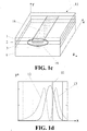
- Interféromètre à guide d'onde optique plan (15, 25, 35, 45) comprenant :- un substrat (8, 28, 38, 48) ;- un guide d'onde bimodal (10, 20, 20', 30, 40) comprenant au moins une couche (1, 2, 3) déposée sur ledit substrat (8, 28, 38, 48), ledit guide d'onde bimodal (10, 20, 20', 30, 40) étant conçu pour prendre en charge des modes de propagation transversale d'ordre zéro et de premier ordre, lesdits modes de propagation transversale ayant une dispersion différente, dans lequel ledit guide d'onde bimodal (10, 20, 20', 30, 40) comprend en outre un moyen de confinement (9) conçu pour confiner une lumière dans une direction latérale, le guide d'onde bimodal (10, 20, 20', 30, 40) étant ainsi conçu pour prendre en charge un mode latéral ;- une zone de détection (21, 31, 41, 51) située dans une zone sélectionnée du côté supérieur dudit guide d'onde bimodal (10, 20, 20', 30, 40), ladite zone de détection (21, 31, 41, 51) étant configurée pour recevoir une stimulation d'entrée chimique, biologique ou physique, ladite stimulation étant capable de changer l'indice de réfraction efficace dudit guide d'onde bimodal (10, 20, 20', 30, 40) ;- un moyen de détection (27, 27', 37, 47) pour mesurer, à la sortie dudit guide d'onde, des changements de l'intensité de rayonnement dus à ladite stimulation d'entrée,
caractérisé en ce que ledit moyen de détection est un photodétecteur à deux sections, l'interféromètre comprenant en outre un moyen apte à enregistrer simultanément la puissance totale et le décalage de la distribution de lumière sortant du guide d'onde bimodal en utilisant ledit photodétecteur à deux sections. - Interféromètre à guide d'onde optique plan (15, 25, 35, 45) selon la revendication 1, comprenant en outre une source de rayonnement électromagnétique (4, 4') configurée pour diriger une lumière optique dans ledit guide d'onde bimodal (10, 20, 20', 30, 40).
- Interféromètre à guide d'onde optique plan (15, 25, 35, 45) selon la revendication 2, dans lequel ladite source de rayonnement électromagnétique (4, 4') est un laser.
- Interféromètre à guide d'onde optique plan (15, 25, 35, 45) selon la revendication 2, dans lequel ladite source de rayonnement électromagnétique est intégrée à la structure du substrat (8, 28, 38, 48).
- Interféromètre à guide d'onde optique plan (15, 25, 35, 45) selon l'une quelconque des revendications précédentes, comprenant en outre un moyen de polarisation.
- Interféromètre à guide d'onde optique plan (15, 25, 35, 45) selon l'une quelconque des revendications précédentes, comprenant en outre un moyen de focalisation.
- Interféromètre à guide d'onde optique plan (15, 25) selon la revendication 6, dans lequel ledit moyen de focalisation est une lentille (22, 52).
- Interféromètre à guide d'onde optique plan (15, 25) selon la revendication 7, dans lequel l'axe central de ladite lentille (22, 52) est configuré pour être désaligné dans la direction transversale par rapport à l'axe de symétrie longitudinal du guide d'onde bimodal (20, 20'), des premier et deuxième modes de propagation transversale étant de ce fait excités à l'intérieur du guide d'onde bimodal (20, 20') lorsqu'une lumière provenant d'une source est directement focalisée à travers ladite lentille vers le guide d'onde bimodal (20, 20').
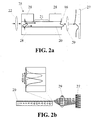
- Interféromètre à guide d'onde optique plan (35) selon l'une quelconque des revendications 1 à 5, comprenant en outre :- un guide d'onde d'entrée (32) relié à une extrémité dudit guide d'onde bimodal (30), ledit guide d'onde d'entrée (32) étant conçu pour prendre en charge un mode unique dans les directions transversale et latérale ;- un guide d'onde de sortie (33) relié à l'autre extrémité dudit guide d'onde bimodal (30), ledit guide d'onde de sortie (33) étant conçu pour prendre en charge un mode unique dans les directions transversale et latérale ;
dans lequel l'épaisseur de chacun desdits guides d'onde d'entrée et de sortie (32, 33) est inférieure à celle dudit guide d'onde bimodal (30), de sorte que, en raison de la géométrie non symétrique de la structure à la jonction dudit guide d'onde d'entrée (32) et dudit guide d'onde bimodal (30), ledit mode unique est divisé en lesdits premier et deuxième modes de propagation transversale. - Interféromètre à guide d'onde optique plan (35) selon la revendication 9, comprenant en outre un moyen pour coupler un rayonnement électromagnétique dans ledit guide d'onde bimodal (30), dans lequel ledit moyen est choisi dans le groupe se composant de : rayonnement longitudinal, focalisation directe, couplage de prisme et couplage de réseau de diffraction.
- Interféromètre à guide d'onde optique plan (35) selon la revendication 9 ou 10, dans lequel la quantité de lumière couplée dans le guide d'onde de sortie (33) dépend de la distribution d'intensité à la jonction entre le guide d'onde bimodal (30) et le guide d'onde de sortie (33).
- Interféromètre à guide d'onde optique plan (45) selon l'une quelconque des revendications 1 à 5, comprenant en outre un moyen de couplage (42) configuré pour coupler, au dit guide d'onde bimodal (40), un mode d'ordre zéro et un mode de premier ordre de lumière avec différents angles d'incidence (θ0, θ1).
- Interféromètre à guide d'onde optique plan (45) selon la revendication 12, dans lequel ledit moyen de couplage (42) est un réseau de diffraction couplé à une entrée dudit guide d'onde bimodal (40).
- Interféromètre à guide d'onde optique plan (15, 25, 35, 45) selon l'une quelconque des revendications précédentes, dans lequel ledit guide d'onde bimodal (10, 20, 20', 30, 40) comprend au moins deux couches.
- Interféromètre à guide d'onde optique plan (15, 25, 35, 45) selon la revendication 14, dans lequel une première couche de guide d'onde a un premier indice de réfraction et une deuxième couche de guide d'onde a un deuxième indice de réfraction, l'indice de réfraction de ladite deuxième couche étant inférieur à celui de ladite première couche de guide d'onde.
- Interféromètre à guide d'onde optique plan (15, 25, 35, 45) selon l'une quelconque des revendications précédentes, dans lequel l'indice de réfraction efficace dudit mode d'ordre zéro et l'indice de réfraction efficace dudit mode de premier ordre sont sensiblement différents.
- Interféromètre à guide d'onde optique plan (15, 25, 35, 45) selon l'une quelconque des revendications précédentes, dans lequel ladite dispersion différente desdits modes de propagation transversale dépend de la vitesse de propagation sur les paramètres dudit guide d'onde.
- Puce comprenant au moins un interféromètre à guide d'onde optique plan (15, 25, 35, 45) selon l'une quelconque des revendications précédentes.
- Capteur comprenant un interféromètre à guide d'onde optique plan (15, 25, 35, 45) selon l'une quelconque des revendications 1 à 17.
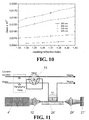
- Procédé de détection comprenant les étapes de :(a) la définition d'une zone de détection (21, 31, 41, 51) dans une zone sélectionnée d'un guide d'onde bimodal (10, 20, 20', 30, 40) d'un interféromètre à guide d'onde optique (15, 25, 35, 45) ;(b) le placement d'une stimulation chimique, biologique ou physique dans ladite zone de détection (21, 31, 41, 51) ;(c) l'introduction ou la provocation de changements de ladite stimulation chimique, biologique ou physique placée dans ladite zone de détection (21, 31, 41, 51) ;(d) le couplage d'un mode d'ordre zéro et d'un mode de premier ordre de rayonnement électromagnétique dans ledit guide d'onde bimodal (10, 20, 20', 30, 40), de telle manière que, lorsque les deux modes traversent la zone de détection (21, 31, 41, 51) définie dans le guide d'onde bimodal (10, 20, 20', 30, 40), ils subissent un retard de phase en fonction des changements de ladite stimulation chimique, biologique ou physique ;(e) à la sortie dudit guide d'onde bimodal (10, 20, 20', 30, 40), la mesure de la réponse dudit mode d'ordre zéro par rapport à la réponse dudit mode de premier ordre ; et(f) la mise en relation de ladite réponse relative des deux modes avec les changements de la stimulation chimique, biologique ou physique, le procédé étant caractérisé en ce que ladite étape de (e) la mesure de la réponse dudit mode d'ordre zéro par rapport à la réponse dudit mode de premier ordre à la sortie dudit guide d'onde bimodal (10, 20, 20', 30, 40) est effectuée en utilisant un photodétecteur à deux sections (47) pour enregistrer simultanément la puissance totale et le décalage de la distribution de lumière sortant du guide d'onde bimodal.
- Procédé de détection selon la revendication 20, dans lequel l'étape de la mesure de la réponse dudit mode d'ordre zéro par rapport à la réponse dudit mode de premier ordre comprend en outre :- la génération d'un motif de franges d'interférences (11, 12, 13) ; et- la mesure d'un déplacement dans le motif d'interférence (11, 12, 13).
- Procédé de détection selon la revendication 21, dans lequel l'étape de la mise en relation de ladite réponse relative des deux modes avec les changements de la stimulation chimique, biologique ou physique comprend :- la mise en relation dudit déplacement dans le motif d'interférence avec la présence de changements de la stimulation chimique, biologique ou physique d'intérêt.
Priority Applications (9)
| Application Number | Priority Date | Filing Date | Title |
|---|---|---|---|
| EP07381053.3A EP2017602B1 (fr) | 2007-07-19 | 2007-07-19 | Interféromètre et capteur basé sur un guide d'onde optique bimodal et procédé de détection |
| ES07381053.3T ES2465619T3 (es) | 2007-07-19 | 2007-07-19 | Interferómetro y sensor basados en una guía de onda óptica bimodal y procedimiento de detección |
| DK07381053.3T DK2017602T3 (da) | 2007-07-19 | 2007-07-19 | Interferometer og sensor baseret på bimodal optisk bølgeleder og registreringsfremgangsmåde |
| PL07381053T PL2017602T3 (pl) | 2007-07-19 | 2007-07-19 | Interferometr i czujnik oparty na światłowodzie bimodalnym oraz sposób wykrywania |
| CN2008801062544A CN101842691B (zh) | 2007-07-19 | 2008-07-18 | 基于双模光波导的干涉仪和传感器以及感测方法 |
| US12/669,307 US8279445B2 (en) | 2007-07-19 | 2008-07-18 | Interferometer and sensor based on bimodal optical waveguides, and detection method |
| JP2010516528A JP2010533849A (ja) | 2007-07-19 | 2008-07-18 | バイモーダル光学導波路に基づく干渉計及びセンサと検出方法 |
| PCT/ES2008/070142 WO2009010624A1 (fr) | 2007-07-19 | 2008-07-18 | Interféromètre et capteur basés sur des guides d'ondes optiques bimodes et procédé de détection |
| CA2693423A CA2693423C (fr) | 2007-07-19 | 2008-07-18 | Interferometre et capteur bases sur des guides d'ondes optiques bimodes et procede de detection |
Applications Claiming Priority (1)
| Application Number | Priority Date | Filing Date | Title |
|---|---|---|---|
| EP07381053.3A EP2017602B1 (fr) | 2007-07-19 | 2007-07-19 | Interféromètre et capteur basé sur un guide d'onde optique bimodal et procédé de détection |
Publications (2)
| Publication Number | Publication Date |
|---|---|
| EP2017602A1 EP2017602A1 (fr) | 2009-01-21 |
| EP2017602B1 true EP2017602B1 (fr) | 2014-02-26 |
Family
ID=38707226
Family Applications (1)
| Application Number | Title | Priority Date | Filing Date |
|---|---|---|---|
| EP07381053.3A Active EP2017602B1 (fr) | 2007-07-19 | 2007-07-19 | Interféromètre et capteur basé sur un guide d'onde optique bimodal et procédé de détection |
Country Status (9)
| Country | Link |
|---|---|
| US (1) | US8279445B2 (fr) |
| EP (1) | EP2017602B1 (fr) |
| JP (1) | JP2010533849A (fr) |
| CN (1) | CN101842691B (fr) |
| CA (1) | CA2693423C (fr) |
| DK (1) | DK2017602T3 (fr) |
| ES (1) | ES2465619T3 (fr) |
| PL (1) | PL2017602T3 (fr) |
| WO (1) | WO2009010624A1 (fr) |
Cited By (2)
| Publication number | Priority date | Publication date | Assignee | Title |
|---|---|---|---|---|
| WO2018162008A1 (fr) | 2017-03-10 | 2018-09-13 | Leibniz-Institut Für Photonische Technologien E.V. | Système et procédé pour détecter des variations de longueur de trajet optique dans un canal nanocapillaire |
| US10816550B2 (en) | 2012-10-15 | 2020-10-27 | Nanocellect Biomedical, Inc. | Systems, apparatus, and methods for sorting particles |
Families Citing this family (21)
| Publication number | Priority date | Publication date | Assignee | Title |
|---|---|---|---|---|
| CN102772863B (zh) * | 2008-10-16 | 2015-05-06 | 株式会社初田制作所 | 灭火器及灭火剂储藏容器 |
| ES2373848T3 (es) * | 2009-02-03 | 2012-02-09 | Optisense B.V. | Interferómetro óptico de guía de ondas integrado. |
| CN102439425A (zh) * | 2009-02-04 | 2012-05-02 | 奥斯坦德姆控股有限公司 | 用于流体分析的系统 |
| US8587490B2 (en) * | 2009-07-27 | 2013-11-19 | New Jersey Institute Of Technology | Localized wave generation via model decomposition of a pulse by a wave launcher |
| GB0921994D0 (en) * | 2009-12-17 | 2010-02-03 | Univ Gent | Methods and systems for optical characterisation |
| CN102735832B (zh) * | 2011-03-30 | 2015-02-18 | 株式会社东芝 | 使用光波导的测定系统 |
| WO2012170352A2 (fr) * | 2011-06-06 | 2012-12-13 | The Regents Of The University Of California | Détection multiplex de particules fluorescentes à l'aide d'une excitation distribuée dans l'espace |
| US9285314B2 (en) | 2011-10-12 | 2016-03-15 | Brown University | Systems and methods enabling high-throughput, real time detection of analytes |
| EP2839387A4 (fr) * | 2012-04-19 | 2016-01-27 | Molecular Sensing Inc | Détection d'événement améliorée pour interférométrie de rétrodiffusion |
| WO2013162528A1 (fr) * | 2012-04-25 | 2013-10-31 | Hewlett-Packard Development Company, L.P. | Analyse de la lumière par interférence de modes |
| CA2897181A1 (fr) * | 2013-01-11 | 2014-07-17 | Lumense, Inc. | Systeme et procede pour detecter de l'ammoniac dans un fluide |
| US9453791B2 (en) * | 2014-07-01 | 2016-09-27 | Octrolix Bv | Flow cytometry system and method |
| DE102015102454A1 (de) | 2015-02-20 | 2016-08-25 | Osram Opto Semiconductors Gmbh | Verfahren zur Strukturierung einer Nitridschicht, strukturierte Dielektrikumschicht, optoelektronisches Bauelement, Ätzverfahren zum Ätzen von Schichten und Umgebungssensor |
| SE540878C2 (en) * | 2015-06-29 | 2018-12-11 | Briano Floria Ottonello | A sensor device and a method of detecting a component in gas |
| CN105572797B (zh) * | 2016-02-15 | 2021-02-26 | 欧阳征标 | 一种太赫兹波脉冲调幅信号与光脉冲调幅信号变换放大器 |
| JP6706814B2 (ja) * | 2016-03-30 | 2020-06-10 | パナソニックIpマネジメント株式会社 | 光検出装置および光検出システム |
| US10996400B2 (en) * | 2016-08-04 | 2021-05-04 | Mitsubishi Electric Research Laboratories, Inc. | Optical waveguide interferometer |
| US10724139B2 (en) * | 2017-06-19 | 2020-07-28 | Wuhan China Star Optoelectronics Semiconductor Display Technology Co., Ltd. | Encapsulation method for OLED Panel |
| EP3460561A1 (fr) | 2017-09-26 | 2019-03-27 | Thomson Licensing | Dispositif pour dévier et focaliser de la lumière |
| US11846574B2 (en) | 2020-10-29 | 2023-12-19 | Hand Held Products, Inc. | Apparatuses, systems, and methods for sample capture and extraction |
| USD987457S1 (en) * | 2021-03-15 | 2023-05-30 | Salvus, Llc | Cartridge |
Citations (1)
| Publication number | Priority date | Publication date | Assignee | Title |
|---|---|---|---|---|
| US5710629A (en) * | 1992-12-10 | 1998-01-20 | Schneider Electric S.A. | Interferometric measuring device forming a spacial interference pattern |
Family Cites Families (12)
| Publication number | Priority date | Publication date | Assignee | Title |
|---|---|---|---|---|
| US4940328A (en) | 1988-11-04 | 1990-07-10 | Georgia Tech Research Corporation | Optical sensing apparatus and method |
| ATE226320T1 (de) * | 1993-03-26 | 2002-11-15 | Hoffmann La Roche | Optisches verfahren und vorrichtung zur analyse von substanzen an sensoroberflächen |
| US20020015155A1 (en) * | 1993-09-21 | 2002-02-07 | Ralf-Dieter Pechstedt | Interferometer integrated on silicon-on-insulator chip |
| US5444249A (en) * | 1994-02-14 | 1995-08-22 | Telaire Systems, Inc. | NDIR gas sensor |
| US5623561A (en) * | 1995-09-29 | 1997-04-22 | Georgia Tech Research Corporation | Integrated optic interferometric sensor |
| CA2348503A1 (fr) * | 1998-10-30 | 2000-05-11 | James V. Suggs | Procedes et capteurs permettant de detecter un acide ou une base et d'en mesurer la concentration |
| GB9927249D0 (en) * | 1999-11-18 | 2000-01-12 | Farfield Sensors Ltd | Device |
| US6646747B2 (en) * | 2001-05-17 | 2003-11-11 | Sioptical, Inc. | Interferometer apparatus and associated method |
| WO2002095365A2 (fr) * | 2001-05-18 | 2002-11-28 | Farfield Sensors Limited | Procede |
| JP2004145246A (ja) | 2002-08-29 | 2004-05-20 | Murata Mfg Co Ltd | 平面型二次元導波路および二次元導波路型光学装置 |
| KR100726206B1 (ko) * | 2006-01-31 | 2007-06-11 | 한국표준과학연구원 | 이상상태 검출을 위한 광섬유 이중모드 간섭형 센서와 이를이용한 이상 탐지 신호처리 방법 |
| US20080043248A1 (en) | 2006-08-18 | 2008-02-21 | Meric Ozcan | Photonic crystal sensors using band edge and/or defect mode modulation |
-
2007
- 2007-07-19 PL PL07381053T patent/PL2017602T3/pl unknown
- 2007-07-19 DK DK07381053.3T patent/DK2017602T3/da active
- 2007-07-19 EP EP07381053.3A patent/EP2017602B1/fr active Active
- 2007-07-19 ES ES07381053.3T patent/ES2465619T3/es active Active
-
2008
- 2008-07-18 US US12/669,307 patent/US8279445B2/en not_active Expired - Fee Related
- 2008-07-18 CA CA2693423A patent/CA2693423C/fr active Active
- 2008-07-18 CN CN2008801062544A patent/CN101842691B/zh not_active Expired - Fee Related
- 2008-07-18 WO PCT/ES2008/070142 patent/WO2009010624A1/fr active Application Filing
- 2008-07-18 JP JP2010516528A patent/JP2010533849A/ja active Pending
Patent Citations (1)
| Publication number | Priority date | Publication date | Assignee | Title |
|---|---|---|---|---|
| US5710629A (en) * | 1992-12-10 | 1998-01-20 | Schneider Electric S.A. | Interferometric measuring device forming a spacial interference pattern |
Cited By (3)
| Publication number | Priority date | Publication date | Assignee | Title |
|---|---|---|---|---|
| US10816550B2 (en) | 2012-10-15 | 2020-10-27 | Nanocellect Biomedical, Inc. | Systems, apparatus, and methods for sorting particles |
| WO2018162008A1 (fr) | 2017-03-10 | 2018-09-13 | Leibniz-Institut Für Photonische Technologien E.V. | Système et procédé pour détecter des variations de longueur de trajet optique dans un canal nanocapillaire |
| DE102017105113B4 (de) | 2017-03-10 | 2021-09-30 | Leibniz-Institut für Photonische Technologien e.V. (Engl.Leibniz Institute of Photonic Technology) | Anordnung und Verfahren für die Erfassung von Änderungen der optischen Weglänge in einem Nano-Kapillarkanal |
Also Published As
| Publication number | Publication date |
|---|---|
| PL2017602T3 (pl) | 2014-09-30 |
| JP2010533849A (ja) | 2010-10-28 |
| US8279445B2 (en) | 2012-10-02 |
| CN101842691A (zh) | 2010-09-22 |
| WO2009010624A1 (fr) | 2009-01-22 |
| US20100271634A1 (en) | 2010-10-28 |
| DK2017602T3 (da) | 2014-06-02 |
| CA2693423C (fr) | 2017-10-31 |
| CA2693423A1 (fr) | 2009-01-22 |
| EP2017602A1 (fr) | 2009-01-21 |
| ES2465619T3 (es) | 2014-06-06 |
| CN101842691B (zh) | 2013-07-03 |
Similar Documents
| Publication | Publication Date | Title |
|---|---|---|
| EP2017602B1 (fr) | Interféromètre et capteur basé sur un guide d'onde optique bimodal et procédé de détection | |
| Wangüemert-Pérez et al. | Subwavelength structures for silicon photonics biosensing | |
| US9164026B2 (en) | Packaged chip for multiplexing photonic crystal microcavity coupled waveguide and photonic crystal slot waveguide devices for chip-integrated label-free detection and absorption spectroscopy with high throughput, sensitivity, specificity, and wide dynamic range | |
| US5663790A (en) | Method and apparatus for determination of refractive index | |
| Chrostowski et al. | Silicon photonic resonator sensors and devices | |
| US6493090B1 (en) | Detection of a substance by refractive index change | |
| CA2233305C (fr) | Capteur interferometrique optique integral | |
| US7447391B2 (en) | Planar-resonator based optical chemo- and biosensor | |
| US7212692B2 (en) | Multiple array surface plasmon resonance biosensor | |
| US10610846B2 (en) | Two-dimensional photonic crystal microarray measurement method and apparatus for highly-sensitive label-free multiple analyte sensing, biosensing, and diagnostic assay | |
| US20090103099A1 (en) | Integrated surface mode biosensor | |
| US9335263B2 (en) | Optical circuit for sensing a biological entity in a fluid and method of configuring the same | |
| JP4118901B2 (ja) | マイクロ計測器 | |
| JP2005274329A (ja) | フォトニック結晶を応用したセンサおよび検出対象物質の検出方法 | |
| Pham et al. | On-chip bulk-index concentration and direct, label-free protein sensing utilizing an optical grated-waveguide cavity | |
| Zhang et al. | Silicon subwavelength-grating microdisks for optical sensing | |
| CN103645158A (zh) | 一种三环型无热化生物传感器 | |
| Duval et al. | Interferometric waveguide biosensors based on Si-technology for point-of-care diagnostic | |
| Wang et al. | Toward on-chip mid-infrared chem/bio sensors using quantum cascade lasers and substrate-integrated semiconductor waveguides | |
| Okubo et al. | Silicon nitride directional coupler interferometer for surface sensing | |
| Rajasekar et al. | Photonic crystal-based sensors for biosensing applications | |
| US20240061174A1 (en) | Method for generating and interacting with polymeric photonic integrated circuits | |
| Werquin et al. | Silicon Ring Resonator-Based Biochips | |
| Janz et al. | Silicon-based microphotonics for biosensing applications | |
| Janz et al. | Engineering light at the sub-wavelength scale using silicon photonics |
Legal Events
| Date | Code | Title | Description |
|---|---|---|---|
| PUAI | Public reference made under article 153(3) epc to a published international application that has entered the european phase |
Free format text: ORIGINAL CODE: 0009012 |
|
| AK | Designated contracting states |
Kind code of ref document: A1 Designated state(s): AT BE BG CH CY CZ DE DK EE ES FI FR GB GR HU IE IS IT LI LT LU LV MC MT NL PL PT RO SE SI SK TR |
|
| AX | Request for extension of the european patent |
Extension state: AL BA HR MK RS |
|
| 17P | Request for examination filed |
Effective date: 20090721 |
|
| 17Q | First examination report despatched |
Effective date: 20090813 |
|
| AKX | Designation fees paid |
Designated state(s): AT BE BG CH CY CZ DE DK EE ES FI FR GB GR HU IE IS IT LI LT LU LV MC MT NL PL PT RO SE SI SK TR |
|
| GRAP | Despatch of communication of intention to grant a patent |
Free format text: ORIGINAL CODE: EPIDOSNIGR1 |
|
| INTG | Intention to grant announced |
Effective date: 20130906 |
|
| GRAS | Grant fee paid |
Free format text: ORIGINAL CODE: EPIDOSNIGR3 |
|
| GRAA | (expected) grant |
Free format text: ORIGINAL CODE: 0009210 |
|
| AK | Designated contracting states |
Kind code of ref document: B1 Designated state(s): AT BE BG CH CY CZ DE DK EE ES FI FR GB GR HU IE IS IT LI LT LU LV MC MT NL PL PT RO SE SI SK TR |
|
| REG | Reference to a national code |
Ref country code: GB Ref legal event code: FG4D |
|
| REG | Reference to a national code |
Ref country code: CH Ref legal event code: EP |
|
| REG | Reference to a national code |
Ref country code: AT Ref legal event code: REF Ref document number: 653873 Country of ref document: AT Kind code of ref document: T Effective date: 20140315 |
|
| REG | Reference to a national code |
Ref country code: IE Ref legal event code: FG4D |
|
| REG | Reference to a national code |
Ref country code: DE Ref legal event code: R096 Ref document number: 602007035193 Country of ref document: DE Effective date: 20140410 |
|
| REG | Reference to a national code |
Ref country code: DK Ref legal event code: T3 Effective date: 20140526 |
|
| REG | Reference to a national code |
Ref country code: NL Ref legal event code: T3 |
|
| REG | Reference to a national code |
Ref country code: ES Ref legal event code: FG2A Ref document number: 2465619 Country of ref document: ES Kind code of ref document: T3 Effective date: 20140606 |
|
| REG | Reference to a national code |
Ref country code: AT Ref legal event code: MK05 Ref document number: 653873 Country of ref document: AT Kind code of ref document: T Effective date: 20140226 |
|
| REG | Reference to a national code |
Ref country code: LT Ref legal event code: MG4D |
|
| PG25 | Lapsed in a contracting state [announced via postgrant information from national office to epo] |
Ref country code: IS Free format text: LAPSE BECAUSE OF FAILURE TO SUBMIT A TRANSLATION OF THE DESCRIPTION OR TO PAY THE FEE WITHIN THE PRESCRIBED TIME-LIMIT Effective date: 20140626 Ref country code: LT Free format text: LAPSE BECAUSE OF FAILURE TO SUBMIT A TRANSLATION OF THE DESCRIPTION OR TO PAY THE FEE WITHIN THE PRESCRIBED TIME-LIMIT Effective date: 20140226 |
|
| REG | Reference to a national code |
Ref country code: CH Ref legal event code: NV Representative=s name: ARNOLD AND SIEDSMA AG, CH |
|
| REG | Reference to a national code |
Ref country code: GR Ref legal event code: EP Ref document number: 20140401000 Country of ref document: GR Effective date: 20140625 |
|
| PG25 | Lapsed in a contracting state [announced via postgrant information from national office to epo] |
Ref country code: SE Free format text: LAPSE BECAUSE OF FAILURE TO SUBMIT A TRANSLATION OF THE DESCRIPTION OR TO PAY THE FEE WITHIN THE PRESCRIBED TIME-LIMIT Effective date: 20140226 Ref country code: AT Free format text: LAPSE BECAUSE OF FAILURE TO SUBMIT A TRANSLATION OF THE DESCRIPTION OR TO PAY THE FEE WITHIN THE PRESCRIBED TIME-LIMIT Effective date: 20140226 Ref country code: CY Free format text: LAPSE BECAUSE OF FAILURE TO SUBMIT A TRANSLATION OF THE DESCRIPTION OR TO PAY THE FEE WITHIN THE PRESCRIBED TIME-LIMIT Effective date: 20140226 Ref country code: PT Free format text: LAPSE BECAUSE OF FAILURE TO SUBMIT A TRANSLATION OF THE DESCRIPTION OR TO PAY THE FEE WITHIN THE PRESCRIBED TIME-LIMIT Effective date: 20140626 |
|
| PG25 | Lapsed in a contracting state [announced via postgrant information from national office to epo] |
Ref country code: LV Free format text: LAPSE BECAUSE OF FAILURE TO SUBMIT A TRANSLATION OF THE DESCRIPTION OR TO PAY THE FEE WITHIN THE PRESCRIBED TIME-LIMIT Effective date: 20140226 Ref country code: BE Free format text: LAPSE BECAUSE OF FAILURE TO SUBMIT A TRANSLATION OF THE DESCRIPTION OR TO PAY THE FEE WITHIN THE PRESCRIBED TIME-LIMIT Effective date: 20140226 |
|
| REG | Reference to a national code |
Ref country code: PL Ref legal event code: T3 |
|
| PG25 | Lapsed in a contracting state [announced via postgrant information from national office to epo] |
Ref country code: RO Free format text: LAPSE BECAUSE OF FAILURE TO SUBMIT A TRANSLATION OF THE DESCRIPTION OR TO PAY THE FEE WITHIN THE PRESCRIBED TIME-LIMIT Effective date: 20140226 Ref country code: CZ Free format text: LAPSE BECAUSE OF FAILURE TO SUBMIT A TRANSLATION OF THE DESCRIPTION OR TO PAY THE FEE WITHIN THE PRESCRIBED TIME-LIMIT Effective date: 20140226 Ref country code: EE Free format text: LAPSE BECAUSE OF FAILURE TO SUBMIT A TRANSLATION OF THE DESCRIPTION OR TO PAY THE FEE WITHIN THE PRESCRIBED TIME-LIMIT Effective date: 20140226 |
|
| REG | Reference to a national code |
Ref country code: DE Ref legal event code: R097 Ref document number: 602007035193 Country of ref document: DE |
|
| PG25 | Lapsed in a contracting state [announced via postgrant information from national office to epo] |
Ref country code: SK Free format text: LAPSE BECAUSE OF FAILURE TO SUBMIT A TRANSLATION OF THE DESCRIPTION OR TO PAY THE FEE WITHIN THE PRESCRIBED TIME-LIMIT Effective date: 20140226 |
|
| PLBE | No opposition filed within time limit |
Free format text: ORIGINAL CODE: 0009261 |
|
| STAA | Information on the status of an ep patent application or granted ep patent |
Free format text: STATUS: NO OPPOSITION FILED WITHIN TIME LIMIT |
|
| 26N | No opposition filed |
Effective date: 20141127 |
|
| REG | Reference to a national code |
Ref country code: DE Ref legal event code: R097 Ref document number: 602007035193 Country of ref document: DE Effective date: 20141127 |
|
| REG | Reference to a national code |
Ref country code: IE Ref legal event code: MM4A |
|
| PG25 | Lapsed in a contracting state [announced via postgrant information from national office to epo] |
Ref country code: SI Free format text: LAPSE BECAUSE OF FAILURE TO SUBMIT A TRANSLATION OF THE DESCRIPTION OR TO PAY THE FEE WITHIN THE PRESCRIBED TIME-LIMIT Effective date: 20140226 |
|
| REG | Reference to a national code |
Ref country code: FR Ref legal event code: PLFP Year of fee payment: 9 |
|
| PG25 | Lapsed in a contracting state [announced via postgrant information from national office to epo] |
Ref country code: GR Free format text: LAPSE BECAUSE OF FAILURE TO SUBMIT A TRANSLATION OF THE DESCRIPTION OR TO PAY THE FEE WITHIN THE PRESCRIBED TIME-LIMIT Effective date: 20150505 Ref country code: IE Free format text: LAPSE BECAUSE OF NON-PAYMENT OF DUE FEES Effective date: 20140719 |
|
| PG25 | Lapsed in a contracting state [announced via postgrant information from national office to epo] |
Ref country code: MC Free format text: LAPSE BECAUSE OF FAILURE TO SUBMIT A TRANSLATION OF THE DESCRIPTION OR TO PAY THE FEE WITHIN THE PRESCRIBED TIME-LIMIT Effective date: 20140226 |
|
| PG25 | Lapsed in a contracting state [announced via postgrant information from national office to epo] |
Ref country code: BG Free format text: LAPSE BECAUSE OF FAILURE TO SUBMIT A TRANSLATION OF THE DESCRIPTION OR TO PAY THE FEE WITHIN THE PRESCRIBED TIME-LIMIT Effective date: 20140226 |
|
| PG25 | Lapsed in a contracting state [announced via postgrant information from national office to epo] |
Ref country code: MT Free format text: LAPSE BECAUSE OF FAILURE TO SUBMIT A TRANSLATION OF THE DESCRIPTION OR TO PAY THE FEE WITHIN THE PRESCRIBED TIME-LIMIT Effective date: 20140226 |
|
| REG | Reference to a national code |
Ref country code: FR Ref legal event code: PLFP Year of fee payment: 10 |
|
| PG25 | Lapsed in a contracting state [announced via postgrant information from national office to epo] |
Ref country code: TR Free format text: LAPSE BECAUSE OF FAILURE TO SUBMIT A TRANSLATION OF THE DESCRIPTION OR TO PAY THE FEE WITHIN THE PRESCRIBED TIME-LIMIT Effective date: 20140226 Ref country code: HU Free format text: LAPSE BECAUSE OF FAILURE TO SUBMIT A TRANSLATION OF THE DESCRIPTION OR TO PAY THE FEE WITHIN THE PRESCRIBED TIME-LIMIT; INVALID AB INITIO Effective date: 20070719 |
|
| REG | Reference to a national code |
Ref country code: FR Ref legal event code: PLFP Year of fee payment: 11 |
|
| REG | Reference to a national code |
Ref country code: FR Ref legal event code: PLFP Year of fee payment: 12 |
|
| PGFP | Annual fee paid to national office [announced via postgrant information from national office to epo] |
Ref country code: NL Payment date: 20211025 Year of fee payment: 15 |
|
| PGFP | Annual fee paid to national office [announced via postgrant information from national office to epo] |
Ref country code: LU Payment date: 20211025 Year of fee payment: 15 Ref country code: FI Payment date: 20211021 Year of fee payment: 15 Ref country code: DK Payment date: 20211022 Year of fee payment: 15 |
|
| PGFP | Annual fee paid to national office [announced via postgrant information from national office to epo] |
Ref country code: GR Payment date: 20211025 Year of fee payment: 15 Ref country code: CH Payment date: 20211025 Year of fee payment: 15 |
|
| PGFP | Annual fee paid to national office [announced via postgrant information from national office to epo] |
Ref country code: PL Payment date: 20211014 Year of fee payment: 15 |
|
| PGFP | Annual fee paid to national office [announced via postgrant information from national office to epo] |
Ref country code: IT Payment date: 20220726 Year of fee payment: 16 Ref country code: GB Payment date: 20220728 Year of fee payment: 16 Ref country code: ES Payment date: 20220802 Year of fee payment: 16 Ref country code: DE Payment date: 20220720 Year of fee payment: 16 |
|
| PGFP | Annual fee paid to national office [announced via postgrant information from national office to epo] |
Ref country code: FR Payment date: 20220728 Year of fee payment: 16 |
|
| REG | Reference to a national code |
Ref country code: DK Ref legal event code: EBP Effective date: 20220731 |
|
| REG | Reference to a national code |
Ref country code: CH Ref legal event code: PL |
|
| REG | Reference to a national code |
Ref country code: NL Ref legal event code: MM Effective date: 20220801 |
|
| PG25 | Lapsed in a contracting state [announced via postgrant information from national office to epo] |
Ref country code: LU Free format text: LAPSE BECAUSE OF NON-PAYMENT OF DUE FEES Effective date: 20220719 Ref country code: LI Free format text: LAPSE BECAUSE OF NON-PAYMENT OF DUE FEES Effective date: 20220731 Ref country code: FI Free format text: LAPSE BECAUSE OF NON-PAYMENT OF DUE FEES Effective date: 20220719 Ref country code: CH Free format text: LAPSE BECAUSE OF NON-PAYMENT OF DUE FEES Effective date: 20220731 |
|
| PG25 | Lapsed in a contracting state [announced via postgrant information from national office to epo] |
Ref country code: GR Free format text: LAPSE BECAUSE OF NON-PAYMENT OF DUE FEES Effective date: 20230209 |
|
| PG25 | Lapsed in a contracting state [announced via postgrant information from national office to epo] |
Ref country code: NL Free format text: LAPSE BECAUSE OF NON-PAYMENT OF DUE FEES Effective date: 20220801 |
|
| PG25 | Lapsed in a contracting state [announced via postgrant information from national office to epo] |
Ref country code: DK Free format text: LAPSE BECAUSE OF NON-PAYMENT OF DUE FEES Effective date: 20220731 |
|
| PG25 | Lapsed in a contracting state [announced via postgrant information from national office to epo] |
Ref country code: PL Free format text: LAPSE BECAUSE OF NON-PAYMENT OF DUE FEES Effective date: 20220719 |
|
| REG | Reference to a national code |
Ref country code: DE Ref legal event code: R119 Ref document number: 602007035193 Country of ref document: DE |
|
| GBPC | Gb: european patent ceased through non-payment of renewal fee |
Effective date: 20230719 |
|
| PG25 | Lapsed in a contracting state [announced via postgrant information from national office to epo] |
Ref country code: DE Free format text: LAPSE BECAUSE OF NON-PAYMENT OF DUE FEES Effective date: 20240201 Ref country code: GB Free format text: LAPSE BECAUSE OF NON-PAYMENT OF DUE FEES Effective date: 20230719 |