EP2017602B1 - Interferometer and sensor based on bimodal optical waveguide and sensing method - Google Patents
Interferometer and sensor based on bimodal optical waveguide and sensing method Download PDFInfo
- Publication number
- EP2017602B1 EP2017602B1 EP07381053.3A EP07381053A EP2017602B1 EP 2017602 B1 EP2017602 B1 EP 2017602B1 EP 07381053 A EP07381053 A EP 07381053A EP 2017602 B1 EP2017602 B1 EP 2017602B1
- Authority
- EP
- European Patent Office
- Prior art keywords
- waveguide
- bimodal
- interferometer
- optical waveguide
- planar optical
- Prior art date
- Legal status (The legal status is an assumption and is not a legal conclusion. Google has not performed a legal analysis and makes no representation as to the accuracy of the status listed.)
- Active
Links
- 230000002902 bimodal effect Effects 0.000 title claims description 82
- 230000003287 optical effect Effects 0.000 title claims description 57
- 238000000034 method Methods 0.000 title claims description 20
- 238000010168 coupling process Methods 0.000 claims description 30
- 230000008878 coupling Effects 0.000 claims description 29
- 238000005859 coupling reaction Methods 0.000 claims description 29
- 238000009826 distribution Methods 0.000 claims description 24
- 230000004044 response Effects 0.000 claims description 23
- 239000000126 substance Substances 0.000 claims description 23
- 230000001902 propagating effect Effects 0.000 claims description 22
- 230000005670 electromagnetic radiation Effects 0.000 claims description 20
- 239000000758 substrate Substances 0.000 claims description 18
- 238000001514 detection method Methods 0.000 claims description 10
- 239000006185 dispersion Substances 0.000 claims description 9
- 238000006073 displacement reaction Methods 0.000 claims description 8
- 230000005855 radiation Effects 0.000 claims description 7
- 230000001419 dependent effect Effects 0.000 claims description 4
- 239000010410 layer Substances 0.000 description 55
- 230000008859 change Effects 0.000 description 29
- 230000035945 sensitivity Effects 0.000 description 22
- 239000012491 analyte Substances 0.000 description 18
- 238000005253 cladding Methods 0.000 description 18
- 239000012071 phase Substances 0.000 description 18
- 239000000463 material Substances 0.000 description 14
- VYPSYNLAJGMNEJ-UHFFFAOYSA-N Silicium dioxide Chemical compound O=[Si]=O VYPSYNLAJGMNEJ-UHFFFAOYSA-N 0.000 description 13
- 239000000243 solution Substances 0.000 description 11
- XUIMIQQOPSSXEZ-UHFFFAOYSA-N Silicon Chemical compound [Si] XUIMIQQOPSSXEZ-UHFFFAOYSA-N 0.000 description 7
- 238000005229 chemical vapour deposition Methods 0.000 description 7
- 238000002474 experimental method Methods 0.000 description 7
- 230000010363 phase shift Effects 0.000 description 7
- 229910052710 silicon Inorganic materials 0.000 description 7
- 239000010703 silicon Substances 0.000 description 7
- PEDCQBHIVMGVHV-UHFFFAOYSA-N Glycerine Chemical compound OCC(O)CO PEDCQBHIVMGVHV-UHFFFAOYSA-N 0.000 description 6
- 229910052581 Si3N4 Inorganic materials 0.000 description 6
- 239000000377 silicon dioxide Substances 0.000 description 6
- HQVNEWCFYHHQES-UHFFFAOYSA-N silicon nitride Chemical compound N12[Si]34N5[Si]62N3[Si]51N64 HQVNEWCFYHHQES-UHFFFAOYSA-N 0.000 description 6
- 239000003153 chemical reaction reagent Substances 0.000 description 5
- 230000003993 interaction Effects 0.000 description 4
- 238000004519 manufacturing process Methods 0.000 description 4
- 238000000206 photolithography Methods 0.000 description 4
- 238000004088 simulation Methods 0.000 description 4
- 239000002250 absorbent Substances 0.000 description 3
- 230000002745 absorbent Effects 0.000 description 3
- 230000008901 benefit Effects 0.000 description 3
- 230000000975 bioactive effect Effects 0.000 description 3
- 230000005684 electric field Effects 0.000 description 3
- 238000005516 engineering process Methods 0.000 description 3
- 238000005530 etching Methods 0.000 description 3
- -1 filaments Chemical compound 0.000 description 3
- 235000011187 glycerol Nutrition 0.000 description 3
- 238000004518 low pressure chemical vapour deposition Methods 0.000 description 3
- 230000035515 penetration Effects 0.000 description 3
- 230000008569 process Effects 0.000 description 3
- 235000012239 silicon dioxide Nutrition 0.000 description 3
- XLYOFNOQVPJJNP-UHFFFAOYSA-N water Substances O XLYOFNOQVPJJNP-UHFFFAOYSA-N 0.000 description 3
- 238000001039 wet etching Methods 0.000 description 3
- 238000004364 calculation method Methods 0.000 description 2
- 238000006243 chemical reaction Methods 0.000 description 2
- 230000005284 excitation Effects 0.000 description 2
- 230000001747 exhibiting effect Effects 0.000 description 2
- 239000007789 gas Substances 0.000 description 2
- 238000002347 injection Methods 0.000 description 2
- 239000007924 injection Substances 0.000 description 2
- 238000002372 labelling Methods 0.000 description 2
- 239000007788 liquid Substances 0.000 description 2
- 238000012544 monitoring process Methods 0.000 description 2
- 230000010355 oscillation Effects 0.000 description 2
- 108090000623 proteins and genes Proteins 0.000 description 2
- 102000004169 proteins and genes Human genes 0.000 description 2
- 238000002310 reflectometry Methods 0.000 description 2
- 239000002356 single layer Substances 0.000 description 2
- 239000012780 transparent material Substances 0.000 description 2
- 108091023037 Aptamer Proteins 0.000 description 1
- OKTJSMMVPCPJKN-UHFFFAOYSA-N Carbon Chemical compound [C] OKTJSMMVPCPJKN-UHFFFAOYSA-N 0.000 description 1
- 229920000049 Carbon (fiber) Polymers 0.000 description 1
- 108020004414 DNA Proteins 0.000 description 1
- 108090000790 Enzymes Proteins 0.000 description 1
- 102000004190 Enzymes Human genes 0.000 description 1
- WQZGKKKJIJFFOK-GASJEMHNSA-N Glucose Natural products OC[C@H]1OC(O)[C@H](O)[C@@H](O)[C@@H]1O WQZGKKKJIJFFOK-GASJEMHNSA-N 0.000 description 1
- 101000760175 Homo sapiens Zinc finger protein 35 Proteins 0.000 description 1
- GPXJNWSHGFTCBW-UHFFFAOYSA-N Indium phosphide Chemical compound [In]#P GPXJNWSHGFTCBW-UHFFFAOYSA-N 0.000 description 1
- 229910000577 Silicon-germanium Inorganic materials 0.000 description 1
- NRTOMJZYCJJWKI-UHFFFAOYSA-N Titanium nitride Chemical compound [Ti]#N NRTOMJZYCJJWKI-UHFFFAOYSA-N 0.000 description 1
- 102100024672 Zinc finger protein 35 Human genes 0.000 description 1
- LEVVHYCKPQWKOP-UHFFFAOYSA-N [Si].[Ge] Chemical compound [Si].[Ge] LEVVHYCKPQWKOP-UHFFFAOYSA-N 0.000 description 1
- 238000002835 absorbance Methods 0.000 description 1
- 238000010521 absorption reaction Methods 0.000 description 1
- 239000002253 acid Substances 0.000 description 1
- 239000004411 aluminium Substances 0.000 description 1
- 229910052782 aluminium Inorganic materials 0.000 description 1
- XAGFODPZIPBFFR-UHFFFAOYSA-N aluminium Chemical compound [Al] XAGFODPZIPBFFR-UHFFFAOYSA-N 0.000 description 1
- 238000004458 analytical method Methods 0.000 description 1
- 238000013459 approach Methods 0.000 description 1
- QVGXLLKOCUKJST-UHFFFAOYSA-N atomic oxygen Chemical compound [O] QVGXLLKOCUKJST-UHFFFAOYSA-N 0.000 description 1
- 239000004917 carbon fiber Substances 0.000 description 1
- 229910021393 carbon nanotube Inorganic materials 0.000 description 1
- 239000002041 carbon nanotube Substances 0.000 description 1
- 238000001311 chemical methods and process Methods 0.000 description 1
- 229910052681 coesite Inorganic materials 0.000 description 1
- 238000007796 conventional method Methods 0.000 description 1
- 229910052906 cristobalite Inorganic materials 0.000 description 1
- 238000009795 derivation Methods 0.000 description 1
- 238000013461 design Methods 0.000 description 1
- 238000010586 diagram Methods 0.000 description 1
- 239000003989 dielectric material Substances 0.000 description 1
- 230000000694 effects Effects 0.000 description 1
- 230000005672 electromagnetic field Effects 0.000 description 1
- 238000010304 firing Methods 0.000 description 1
- 239000012634 fragment Substances 0.000 description 1
- ZZUFCTLCJUWOSV-UHFFFAOYSA-N furosemide Chemical compound C1=C(Cl)C(S(=O)(=O)N)=CC(C(O)=O)=C1NCC1=CC=CO1 ZZUFCTLCJUWOSV-UHFFFAOYSA-N 0.000 description 1
- 239000007792 gaseous phase Substances 0.000 description 1
- 239000011521 glass Substances 0.000 description 1
- 239000008103 glucose Substances 0.000 description 1
- 238000002513 implantation Methods 0.000 description 1
- 238000011065 in-situ storage Methods 0.000 description 1
- 230000010354 integration Effects 0.000 description 1
- 230000002452 interceptive effect Effects 0.000 description 1
- 239000007791 liquid phase Substances 0.000 description 1
- 239000011159 matrix material Substances 0.000 description 1
- 238000005259 measurement Methods 0.000 description 1
- VNWKTOKETHGBQD-UHFFFAOYSA-N methane Chemical compound C VNWKTOKETHGBQD-UHFFFAOYSA-N 0.000 description 1
- 238000004377 microelectronic Methods 0.000 description 1
- 238000002156 mixing Methods 0.000 description 1
- 230000003647 oxidation Effects 0.000 description 1
- 238000007254 oxidation reaction Methods 0.000 description 1
- 229910052760 oxygen Inorganic materials 0.000 description 1
- 239000001301 oxygen Substances 0.000 description 1
- 230000002572 peristaltic effect Effects 0.000 description 1
- 229920002120 photoresistant polymer Polymers 0.000 description 1
- 229920000642 polymer Polymers 0.000 description 1
- 229920001296 polysiloxane Polymers 0.000 description 1
- 239000002243 precursor Substances 0.000 description 1
- 230000000644 propagated effect Effects 0.000 description 1
- HBMJWWWQQXIZIP-UHFFFAOYSA-N silicon carbide Chemical compound [Si+]#[C-] HBMJWWWQQXIZIP-UHFFFAOYSA-N 0.000 description 1
- 229910010271 silicon carbide Inorganic materials 0.000 description 1
- 229910052814 silicon oxide Inorganic materials 0.000 description 1
- 239000011343 solid material Substances 0.000 description 1
- 229910052682 stishovite Inorganic materials 0.000 description 1
- 238000006467 substitution reaction Methods 0.000 description 1
- 238000002198 surface plasmon resonance spectroscopy Methods 0.000 description 1
- 239000010409 thin film Substances 0.000 description 1
- 238000012546 transfer Methods 0.000 description 1
- 229910052905 tridymite Inorganic materials 0.000 description 1
- WFKWXMTUELFFGS-UHFFFAOYSA-N tungsten Chemical compound [W] WFKWXMTUELFFGS-UHFFFAOYSA-N 0.000 description 1
- 229910052721 tungsten Inorganic materials 0.000 description 1
- 239000010937 tungsten Substances 0.000 description 1
Images


Classifications
-
- G—PHYSICS
- G01—MEASURING; TESTING
- G01N—INVESTIGATING OR ANALYSING MATERIALS BY DETERMINING THEIR CHEMICAL OR PHYSICAL PROPERTIES
- G01N21/00—Investigating or analysing materials by the use of optical means, i.e. using sub-millimetre waves, infrared, visible or ultraviolet light
- G01N21/17—Systems in which incident light is modified in accordance with the properties of the material investigated
- G01N21/41—Refractivity; Phase-affecting properties, e.g. optical path length
- G01N21/45—Refractivity; Phase-affecting properties, e.g. optical path length using interferometric methods; using Schlieren methods
-
- G—PHYSICS
- G01—MEASURING; TESTING
- G01N—INVESTIGATING OR ANALYSING MATERIALS BY DETERMINING THEIR CHEMICAL OR PHYSICAL PROPERTIES
- G01N21/00—Investigating or analysing materials by the use of optical means, i.e. using sub-millimetre waves, infrared, visible or ultraviolet light
- G01N21/75—Systems in which material is subjected to a chemical reaction, the progress or the result of the reaction being investigated
- G01N21/77—Systems in which material is subjected to a chemical reaction, the progress or the result of the reaction being investigated by observing the effect on a chemical indicator
- G01N21/7703—Systems in which material is subjected to a chemical reaction, the progress or the result of the reaction being investigated by observing the effect on a chemical indicator using reagent-clad optical fibres or optical waveguides
-
- G—PHYSICS
- G02—OPTICS
- G02B—OPTICAL ELEMENTS, SYSTEMS OR APPARATUS
- G02B6/00—Light guides; Structural details of arrangements comprising light guides and other optical elements, e.g. couplings
- G02B6/10—Light guides; Structural details of arrangements comprising light guides and other optical elements, e.g. couplings of the optical waveguide type
- G02B6/12—Light guides; Structural details of arrangements comprising light guides and other optical elements, e.g. couplings of the optical waveguide type of the integrated circuit kind
- G02B6/122—Basic optical elements, e.g. light-guiding paths
- G02B6/124—Geodesic lenses or integrated gratings
-
- G—PHYSICS
- G01—MEASURING; TESTING
- G01N—INVESTIGATING OR ANALYSING MATERIALS BY DETERMINING THEIR CHEMICAL OR PHYSICAL PROPERTIES
- G01N21/00—Investigating or analysing materials by the use of optical means, i.e. using sub-millimetre waves, infrared, visible or ultraviolet light
- G01N21/17—Systems in which incident light is modified in accordance with the properties of the material investigated
- G01N21/41—Refractivity; Phase-affecting properties, e.g. optical path length
- G01N21/45—Refractivity; Phase-affecting properties, e.g. optical path length using interferometric methods; using Schlieren methods
- G01N2021/458—Refractivity; Phase-affecting properties, e.g. optical path length using interferometric methods; using Schlieren methods using interferential sensor, e.g. sensor fibre, possibly on optical waveguide
-
- G—PHYSICS
- G01—MEASURING; TESTING
- G01N—INVESTIGATING OR ANALYSING MATERIALS BY DETERMINING THEIR CHEMICAL OR PHYSICAL PROPERTIES
- G01N21/00—Investigating or analysing materials by the use of optical means, i.e. using sub-millimetre waves, infrared, visible or ultraviolet light
- G01N21/75—Systems in which material is subjected to a chemical reaction, the progress or the result of the reaction being investigated
- G01N21/77—Systems in which material is subjected to a chemical reaction, the progress or the result of the reaction being investigated by observing the effect on a chemical indicator
- G01N2021/7769—Measurement method of reaction-produced change in sensor
- G01N2021/7779—Measurement method of reaction-produced change in sensor interferometric
-
- G—PHYSICS
- G02—OPTICS
- G02B—OPTICAL ELEMENTS, SYSTEMS OR APPARATUS
- G02B6/00—Light guides; Structural details of arrangements comprising light guides and other optical elements, e.g. couplings
- G02B6/10—Light guides; Structural details of arrangements comprising light guides and other optical elements, e.g. couplings of the optical waveguide type
- G02B6/12—Light guides; Structural details of arrangements comprising light guides and other optical elements, e.g. couplings of the optical waveguide type of the integrated circuit kind
- G02B2006/12083—Constructional arrangements
- G02B2006/12107—Grating
-
- G—PHYSICS
- G02—OPTICS
- G02B—OPTICAL ELEMENTS, SYSTEMS OR APPARATUS
- G02B6/00—Light guides; Structural details of arrangements comprising light guides and other optical elements, e.g. couplings
- G02B6/10—Light guides; Structural details of arrangements comprising light guides and other optical elements, e.g. couplings of the optical waveguide type
- G02B6/12—Light guides; Structural details of arrangements comprising light guides and other optical elements, e.g. couplings of the optical waveguide type of the integrated circuit kind
- G02B2006/12133—Functions
- G02B2006/12152—Mode converter
-
- G—PHYSICS
- G02—OPTICS
- G02B—OPTICAL ELEMENTS, SYSTEMS OR APPARATUS
- G02B6/00—Light guides; Structural details of arrangements comprising light guides and other optical elements, e.g. couplings
- G02B6/10—Light guides; Structural details of arrangements comprising light guides and other optical elements, e.g. couplings of the optical waveguide type
- G02B6/12—Light guides; Structural details of arrangements comprising light guides and other optical elements, e.g. couplings of the optical waveguide type of the integrated circuit kind
- G02B2006/12133—Functions
- G02B2006/12159—Interferometer
-
- G—PHYSICS
- G02—OPTICS
- G02B—OPTICAL ELEMENTS, SYSTEMS OR APPARATUS
- G02B6/00—Light guides; Structural details of arrangements comprising light guides and other optical elements, e.g. couplings
- G02B6/10—Light guides; Structural details of arrangements comprising light guides and other optical elements, e.g. couplings of the optical waveguide type
- G02B6/14—Mode converters
-
- G—PHYSICS
- G02—OPTICS
- G02B—OPTICAL ELEMENTS, SYSTEMS OR APPARATUS
- G02B6/00—Light guides; Structural details of arrangements comprising light guides and other optical elements, e.g. couplings
- G02B6/24—Coupling light guides
- G02B6/26—Optical coupling means
- G02B6/32—Optical coupling means having lens focusing means positioned between opposed fibre ends
Definitions
- the present invention relates to interferometers and sensors based on optical waveguides, and more particularly, to interferometers and sensors based on bimodal optical waveguides.
- Detection of a molecule e.g. protein, glucose or binding between the molecules is a common issue.
- the amount of reagent or the concentration of the molecules in the solution may be low and highly sensitive devices are required for the detection of the molecules.
- the detection can be conducted using various methods and techniques.
- nanomechanical and optical devices such as Mach-Zhender interferometers, Surface Plasmon Resonance, Young interferometers, Fabry-Perot interferometers and slab interferometers. Mach-Zhender and Young interferometers are compact devices based on optical waveguides which were introduced long time ago and have been well studied.
- Interferometers have normally two branches, one of which, when the interferometer acts as a sensing device, is provided with a sensing window, the other one being a reference. Reagent flowing through the sensing window interacts with the molecules previously immobilised over the waveguide in the window. This changes the refractive index of the cladding layer of the waveguide and subsequently the velocity of light propagation along this waveguide.
- interferometers with two branches have the drawback of having difficulties in accurate splitting the light. If not well fabricated, the critical symmetry of the Y junction leaves the interferometer prone to reduced modulation depth and losses in sensitivity.
- Sensitivity is defined by the depth of penetration of the evanescent field of the waveguide into the analyte conjugate to the waveguide, that is to say, into the analyte which is in contact with the waveguide. Penetration depth significantly increases if the waveguide thickness is reduced. This involves difficulties in light coupling due to the mismatch between the intensity distribution of the waveguide propagating mode of thin waveguides and the intensity distribution of a conventional light source.
- the working principle of the structure described in JP2004145246 is based on interference of two propagating modes in a plane type bimodal waveguide.
- Figure 5 shows such a waveguide.
- the physical structure is three-dimensional, from the properties point of view the structure is bidimensional:
- X axis which is the direction of light propagation
- the structure has a step or rib 500 which defines a change in thickness along this longitudinal axis.
- transverse direction referred to in figure 5 as Y axis
- the properties (i.e. refractive index) of the waveguide materials change.
- lateral direction referred to in figure 5 as Z axis
- the waveguide structure is uniform, because its properties do not change along this lateral direction.
- the structure is therefore a bidimensional one (from the propagation point of view, it has a longitudinal dimension and a transverse one).
- the dimensionality of the device of JP2004145246 prevents the fabrication of long and narrow interferometers capable detecting ultra small changes in the refractive index of the cladding layer.
- US 4940328 A discloses a bimodal waveguide supporting lateral mode, with limited sensitivity.
- the present invention exploits bimodal waveguide structures where different relative phase retardation between the two propagating modes accumulates when it is subjected to a structural change.
- the present invention relates to an optical waveguide interferometer comprising a bimodal waveguide whose propagating modes dispersion is mode order sensitive according to claim 1.
- a planar optical waveguide interferometer which comprises a substrate; a bimodal waveguide comprising at least one layer deposited on the substrate, the bimodal waveguide being designed for supporting a zero-order and a first-order transversal propagating modes, the transversal propagating modes having different dispersion; a sensing window located in a selected area of the upper side of the bimodal waveguide, the sensing window being configured for receiving a chemical, biological or physical input stimulus, that stimulus being capable of changing the effective refractive index of the bimodal waveguide.
- the bimodal waveguide further comprises confining means designed for confining light in lateral direction, the bimodal waveguide being thus designed for supporting one lateral mode.
- the interferometer preferably comprises an electromagnetic radiation source configured for leading optical light into the bimodal waveguide.
- This source is more preferably a laser.
- the source is integrated within the structure of the substrate.
- the interferometer further comprises polarising means.
- the interferometer further comprises focussing means.
- the focussing means is a lens.
- the central axis of the lens is configured to be misaligned in the transversal direction with respect to the longitudinal symmetry axis of the bimodal waveguide, thereby a first and a second transversal propagating modes being excited within the bimodal waveguide when light from a source is directly focussed through said lens towards the bimodal waveguide.
- the interferometer further comprises an input waveguide connected at one end of the bimodal waveguide, this input waveguide being designed for supporting a single mode in both transversal and lateral directions; and an output waveguide connected at the other end of the bimodal waveguide, this output waveguide being designed for supporting a single mode in both transversal and lateral directions.
- the thickness of each of the input and output waveguides is less than that of the bimodal waveguide, such that due to the non-symmetrical geometry of the structure at the junction of the input waveguide and the bimodal waveguide, the single mode is split into first and second transversal propagating modes.
- the interferometer further comprises means for coupling electromagnetic radiation into the bimodal waveguide, this means being chosen from the group formed by: end-fire, direct focusing, prism coupling and diffraction grating coupling.
- This means being chosen from the group formed by: end-fire, direct focusing, prism coupling and diffraction grating coupling.
- the amount of light coupled into the output waveguide depends on the intensity distribution at the junction between the bimodal waveguide and the output waveguide.
- the interferometer further comprises coupling means configured for coupling to the bimodal waveguide first and second order modes of light with different incidence angles.
- the coupling means is a diffraction grating coupled to an input of the bimodal waveguide.
- the bimodal waveguide comprises at least two layers.
- a first waveguide layer has a first refractive index and a second waveguide layer has a second refractive index.
- the refractive index of the second layer is lower than that of the first waveguide layer.
- the effective refractive index of the zero-order mode and that of the first-order mode are substantially different. This different dispersion of the transversal propagating modes depends on the propagation velocity on the parameters of the waveguide.
- the interferometer further comprises detection means for measuring at the output of the waveguide changes in the radiation intensity due to the input stimulus.
- the detection means is a two sectional photodetector.
- Another aspect of the invention refers to chip comprising at least one planar optical waveguide interferometer like the above-mentioned one.
- Another aspect of the invention refers to a sensor comprising a planar optical waveguide interferometer like the above-mentioned one.
- the present invention relates to a sensing method comprising the steps of: (a) defining a sensing window in a selected area of a bimodal waveguide of an optical waveguide interferometer; (b) placing a chemical, biological or physical stimulus in the sensing window; (c) introducing or causing changes in the stimulus; (d) coupling a zero-order mode and a first-order mode of electromagnetic radiation into the bimodal waveguide, in such a way that when both modes travel through the sensing window defined in the bimodal waveguide, they suffer a phase delay which is dependent on the changes in the stimulus; (e) at the output of the bimodal waveguide, measuring the response of the zero-order mode relative to the response of the first-order mode; and (f) relating that relative response of both modes to the changes in the stimulus.
- the step of measuring the response of the zero-order mode relative to that of the first-order mode further comprises: generating a pattern of interference fringes; and measuring a displacement in the interference pattern.
- the step of relating the relative response of both modes to the changes in the stimulus further comprises relating the displacement in the interference pattern to the presence of changes in the stimulus of interest.
- a "transverse mode" of a light beam of electromagnetic radiation is a particular intensity pattern of radiation measured along a line formed by a plane (plane 1 or plane YOZ) perpendicular to the propagation direction of light beam and a plane (plane 2 or plane XOY) perpendicular to a waveguide structure and going along the propagation direction.
- plane plane 1 or plane YOZ
- plane 2 or plane XOY plane 2 or plane XOY
- a "lateral mode" of a light beam of electromagnetic radiation is a particular intensity pattern of radiation measured along a line formed by a plane (plane 1 or plane YOZ) perpendicular to the propagation direction of light beam and the plane (plane 3 or plane XOZ) in which a waveguide structure lies, and going along the propagation direction.
- plane 1 or plane YOZ plane perpendicular to the propagation direction of light beam
- plane 3 or plane XOZ plane in which a waveguide structure lies, and going along the propagation direction.
- the term “horizontal” is to be considered as a synonym of "lateral".
- the transverse and lateral modes can be classified into TE (transverse electric) modes and TM (transverse magnetic) modes.
- TE modes are those which have no electric field in the direction of propagation
- TM modes are those which have no magnetic field in the direction of propagation.
- the "dispersion" of a waveguide mode is a dependence of the propagation velocity of said mode on the parameters of the waveguide and its surrounding layers.
- Analyte is any solution containing a substance which is to be detected by the interferometer and sensor of the present invention.
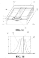
- Figure 1a shows a schematic representation of a single optical waveguide 10 which supports two modes of the present invention.
- the two modes the waveguide 10 is capable of supporting are transversal modes (TE or TM): a fundamental TE or TM mode and a first order TE or TM mode.
- TE or TM transversal modes
- two lateral modes could be chosen, in order to overcome the already mentioned disadvantages derived from structures confining two lateral modes, a structure configured to confine two transversal modes is chosen and designed.
- This optical waveguide 10 acts as an interferometer.
- the optical waveguide 10 comprises at least one layer 2 of optically transparent material deposited in a laminar fashion onto a substrate 8.
- the waveguide 10 comprises several layers 1 2 3 of optically transparent material deposited in a laminar fashion onto a substrate 8.
- Layer 2 is of higher refractive index than that of adjacent layers 1 3. Therefore, in this case the optical waveguide 10 is an optical slab waveguide.
- the waveguide 10 can have a single layer: One layer 1 over the substrate is enough, because, as will be explained later, an analyte deposited over the upper layer (which can be the only layer) also forms a layer (a covering layer) above the waveguide 10.
- the working principle of the interferometer according to which light travels over a structure with areas having different refractive index is fulfilled, said two areas being the monolayer waveguide 10 (supported on a substrate 8) and the analyte or covering layer deposited thereon.
- a plurality of layers 1 2 3 are used in order to optimise the structure.
- Waveguide 10 further comprises confining means 9 which are capable of confining light in lateral direction. Thanks to this confining means 9, the waveguide 10 can support at least one lateral mode.
- narrow light beams having width of less than about 100 ⁇ m
- light inside such waveguides gets very divergent, which means that after propagation transversally for several millimetres, the light beam diverges and expands several millimetres in lateral direction.
- single mode operation in lateral direction is extremely difficult to maintain in a simple, planar structure is used. What is more, the longer the waveguide is, the more difficult it is to maintain single mode operation in lateral direction. For this reason, confining means such as ribs, ridges, etc. are necessary.
- Single mode operation in lateral direction also facilitates the modelling of the interferometer when working as a sensor and makes predictable its behaviour.
- Non-limiting examples of confining means 9 which can provide such confinement are a rib, a ridge or a gradient.
- Appropriate waveguides are therefore: rib, ridge, gradient or other waveguide structures.
- Waveguide 10 therefore permits propagation of incident electromagnetic radiation in the direction represented by the length of the waveguide 10, that is to say, in the direction represented by the arrow which comes out of optical source 4.
- the waveguide 10 is preferably a rectangular waveguide, so that the modes are laterally and transversally confined.
- the fact that the waveguide is rectangular does not mean that in the plane perpendicular to the propagation direction the waveguide has necessarily rectangular profile.
- the waveguide cross section may have a small step, forming a rib waveguide structure.
- waveguide 10 is a rib waveguide.
- the waveguide 10 comprises a rib 9 in the lateral direction (according to the scheme of figure 5 ).
- This rib 9 implies that the thickness of the waveguide 10 varies along said lateral direction.
- Figure 1b shows another view of the same waveguide 10 having a rib 9.
- Reference 19 in figure 1c represents another type of waveguide 10.
- the three propagation directions are illustrated: longitudinal, X, direction (which is the direction of light propagation), transversal direction, Y, and lateral direction, Z.
- the structure of the present invention is homogeneous in the direction of light propagation (longitudinal direction), while the structure disclosed in JP2004145246 is homogeneous or uniform in lateral direction.
- the structure also comprises a sensing window or area which is formed over a surface of the waveguide using standard photolithography and wet etching. This sensing window is illustrated in figures 2 to 4 .
- the waveguide confines single mode light (thus is able to propagate light) for several centimetres without light divergence in lateral direction.
- Single mode operation in lateral direction is required because of the following reasons: First, when the waveguide is used as an interferometer or as a sensor, it helps to avoid ambiguities in monitoring the interference pattern created at the waveguide end. Second, narrow waveguides, which can only be implemented by two dimensional structures (i.e. ribs, ridges, etc.) allow squeezing the sensing area to a fraction of square millimetre. The sensing area can vary from about 0.05 to about 1 mm 2 . As a matter of example, a 15 mm long and 0.01 mm wide waveguide has an area of 0.15 mm 2 .
- Sensitivity is very important in the device of the present invention.
- the structure needs to be long enough in order to work as a waveguide interferometer, because its sensitivity is proportional to the length of the sensing window or area or to the length of the bimodal waveguide.
- the length of the structure is preferably in the following range: between around 0.5 and around 5 cm.
- Figure 1c shows how the waveguide 10 formed by an implanted waveguide may be fabricated by implantation.
- Reference 18 represents an area wherein waveguide 19 is implanted.
- the refractive index changes over this area 18.
- Such a waveguide has spatial change in index of refraction in transversal and lateral directions, while geometrically it keeps being a plane slab structure.
- Light from a source 4 may be transmitted to the input end 5 of the waveguide 10 so as to illuminate layer 2.
- the light source 4 provides light having a wavelength falling within the visible or near infrared range, such as between around 400 and around 1600 nm.
- Light source 4 is preferably a laser source.
- measuring devices 7 are detectors, such as one or more photodiodes. Where more than one photodetector is used, they are arranged in an array, such as a two-dimensional photodiode array or a CCD camera.
- the two transversal modes are capable of exhibiting a measurable relative response to a change in the wavelength of incident electromagnetic radiation or in a localised environment. If the refractive index of layer 1 locally changes, a different relative phase delay accumulates and the intensity distribution is modified accordingly.
- Optical waveguide transversal modes have an electric field that is distributed among the layers 1 2 3 and in some cases through the substrate 8 of the waveguide structure 10. The relative amount of power contained in the layers 1 2 3 determines the "effective refractive index" of the waveguide mode. In turn, the effective refractive index of a mode determines the propagation speed of that mode and therefore the extent of phase delay that can be accumulated as the mode travels through the waveguide 10.
- the field distribution also changes, thereby resulting in a change in the effective refractive index. If the dispersion properties of the modes are different, then the change in effective refractive index can be quite large.
- the propagation constants for the fundamental and the first order modes depend on the refractive index of the upper or covering layer. As already mentioned, when the optical waveguide 10 works as an interferometer, and an analyte is deposited over the upper layer 1, the analyte works as a covering layer. In other words, it is necessary that the dispersion (that is to say, the dependence of the propagation constants on the refractive index) is different for each mode.
- the interference pattern of the two modes at the end of the waveguide is dependent on the refractive index of the conjugate layers, and therefore on the analyte solution refractive index.
- Figure 1d represents an example of the intensity distribution of the propagating modes in the transversal direction.
- the distance in transversal direction is indicated in X axis in nm.
- the normalised intensity of the electric field is indicated in the Y axis (the magnitude not being so important as the actual response or shape).
- reference 11 represents a distribution of intensity of the fundamental mode.
- References 12 and 13 represent the distribution of intensity of the first order mode. As can be seen in figure 1d , the dispersion effect is due to the markedly different power distribution between both modes.
- the optical waveguide structure 10 forming an optical interferometer may be advantageously manufactured using any suitable combination of conventional materials.
- conventional methods of fabrication are those based on Chemical Vapor Deposition (CVD), such as Plasma Enhancement Chemical Vapor Deposition (PECVD) or Low Pressure Chemical Vapor Deposition (LPCVD).
- CVD Chemical Vapor Deposition
- PECVD Plasma Enhancement Chemical Vapor Deposition
- LPCVD Low Pressure Chemical Vapor Deposition
- Chemical Vapor Deposition is a chemical process used to produce high-purity, high-performance solid materials, such as thin films.
- the wafer (substrate) is exposed to one or more volatile precursors, which react and/or decompose on the substrate surface to produce the desired deposit.
- Microfabrication processes widely use CVD to deposit materials in various forms, including: monocrystalline, polycrystalline, amorphous and epitaxial. These materials include: silicon, carbon fiber, filaments, carbon nanotubes, SiO 2 , silicon-germanium, tungsten, silicon carbide, silicon nitride, silicon oxynitride, titanium nitride, and various high-k dielectrics.
- the refractive index of a silicon oxynitride optical waveguide of constant thickness may be selected at any level in the range of 1.457 to 2.00.
- the first waveguide mode and second waveguide mode are capable of exhibiting a measurable relative response to a change in a localised environment caused by the introduction of changes in a physical, biological and/or chemical stimulus of interest.
- This response is caused by the evanescent field of the modes as they extend into the localised environment.
- An example of introduction of a change in a stimulus is a change in the refractive index of the material (i.e. analyte) placed in that environment.
- the first and second waveguide modes accumulate different relative phase delay, thereby causing a measurable relative response.
- planar optical waveguide interferometer 15 can advantageously be used to detect the presence of changes in a physical, biological and/or chemical stimulus in an analyte introduced into the localised environment.
- the optical waveguide interferometer thus becomes a chemical sensor waveguide interferometer or a sensor based on optical waveguide.
- Non-limiting examples of interaction of the stimulus with the waveguide modes are: binding interaction, absorbance interaction or any other interaction.
- a gaseous or liquid phase analyte comprising chemical stimuli may be introduced into the localised environment of the optical waveguide interferometer.
- a chemical reaction may take place in said environment, causing changes in the nature of the chemical stimuli in situ, thereby causing a change in the localised environment.
- the localised environment is preferably an area or surface of the upper layer 1 of the optical waveguide 10 (not illustrated in figures 1a-1c ).
- This sensing layer may comprise a material chosen from the following group: absorbent materials and bioactive materials.
- absorbent materials are polymeric materials, such as a polysiloxane or imprinted polymers.
- An absorbent material is capable of absorbing gases, liquids or vapours comprising a chemical stimulus of interest.
- bioactive materials are those comprising monoclonal and polyclonal antibodies, enzymes, DNA fragments, RNA, aptamers, PNAs, functional proteins or whole cells.
- a bioactive material may be appropriate for liquid or gas phase biosensing.
- An interference pattern is generated inside the bimodal waveguide 10 (acting as an interferometer) when electromagnetic radiation propagates along the waveguide 10.
- the above mentioned changes in a stimulus in a localised environment or sensing layer, or a change in wavelength, may be calculated from the relative phase shift of the interference pattern.
- the measurable response to said change is represented by a displacement of the fringes in the interference pattern.
- the relative phase shift of the radiation within the interferometer may be calculated by measuring said displacement in the fringes.
- the electromagnetic radiation is coupled into free space.
- the interference pattern can thus be recorded in a conventional manner (such as using a single detector 7 which measures the changes in the radiation intensity or using a plurality of such detectors 7 which monitor the changes occurring in a number of fringes or in the entire interference pattern).
- detectors 7 are preferably one or more photodetectors. Where more than one photodetector is used, they are arranged in an array, such as a two-dimensional photodiode array.
- light from a source 4 is focussed to the input end 5 of the waveguide 10 and propagated in the form of electromagnetic radiation, which can be coupled into the first and second waveguide modes in different ways.
- radiation is simply coupled into the waveguide 10 via an end face 5 of said waveguide 10. This is also called “an end firing procedure”.
- the light source i.e. laser
- substrates 8 are silicon and indium phosphide substrates.
- the interferometer 15 comprises other coupling means for coupling the incident electromagnetic radiation into the first (fundamental) and second (first-order) waveguide modes of the waveguide 10. This coupling of the two modes is done substantially simultaneously.
- Non-limiting examples of coupling means, apart from end-fire, are direct focusing (for example, by means of a HeNe laser), prism coupling, diffraction grating coupling or mirror coupling.
- the incident light or electromagnetic radiation may be oriented (e.g. plane polarised) as desired using appropriate polarising means.
- polarising means are polarising cube beam splitters, linear glass polarisers and wire grid polarisers.
- the incident light or electromagnetic radiation may be focussed using focussing means.
- focussing means are: a lens, a microlens and an optical system comprising a series of lenses.
- the output electromagnetic radiation pattern may be projected towards the above mentioned detector by means of projecting means.
- projecting means are objective lenses, lenses and direct projection onto multi sectional photodetector.
- interferometers based on bimodal waveguides and sensors based on interferometers are described:
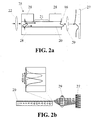
- Figure 2 illustrates an example of interferometer 25 which comprises a bimodal waveguide 20, formed by one or more layers as illustrated in figures 1a, 1b and 1c .
- the waveguide 20 comprises a sensing window 21, wherein an analyte can be deposited.
- Waveguide modes (the fundamental and the first order ones) are excited in the waveguide 20 using direct focusing of light from a laser source (not shown in figure 2 ) by means of an objective lens 22.
- a structure is considered non-symmetrical in transverse direction if the distribution of the refractive index across the structure in transversal direction is not symmetrical with respect to the symmetry axis of the structure.
- the symmetry axis of the structure is an axis going in the direction of light propagation and crossing the plane perpendicular to the light propagation direction in a point where maximum intensity of electromagnetic field distribution of a transverse fundamental mode is located.
- the structure of figure 5 is thus non-symmetrical. Because the structure is not symmetrical and the central axis of the objective lens 22 can be misaligned in the transversal direction with respect to the symmetry axis of the waveguide layer, both the zero (fundamental) and the first order modes are excited. The two transversal modes propagate with different velocities and pass by the sensing window 21.
- the interference pattern formed at the output end 16 of the waveguide 20 is projected on a two sectional photodetector (TSP) 27 using an objective lens 29 as a projecting and magnifying means.
- the position of the maximum of the interference pattern is defined, among other parameters, such as the refractive index, the thickness of each layer, the length of the waveguide and the width of the waveguide, by the initial phase of the excited waves and by the refractive index of the analyte passing through the sensing window 21. It is thus registered the change in the refractive index of the covering layer (measured in the sensing window) caused by a chemical or biological reaction which has occurred on the waveguide surface or by changes in the analyte solution.
- Blocks 28 refer to the walls of a microfluidic cell which can be attached to the waveguide 20 in order to provide flow and exchange of the analyte. They are not part of the present invention.
- Figure 2b shows an implementation of the example of figure 2a .
- the interference pattern in the transversal direction can be distributed with the maximum located in the lower or in the upper part of the waveguide, as shown in figure 2b , where the distributions of light intensities in the waveguide cross section are shown in the inset.
- the distributions are built for a waveguide with refractive index of 2.0 (silicon nitride) and with thickness of 400 nm.
- the phase difference between the modes varies by ⁇ radian from one curve to the other. Under certain conditions the difference between the energies concentrated in the top and in the bottom sections of the photodetector can reach -17 dB.
- the output intensity is proportional to the amount of light coupled into the waveguide at the input.
- the total light power at the exit is proportional to the power coupled at the input except for some changes due to reflectivity from the output facet, which according to simulations is slightly changing with the interference pattern movement. Assuming that the function of the reflectivity change is known, the ambiguities due to coupling efficiency variations can be reduced, because monitoring with a two sectional photodetector (TSP) allows to register simultaneously both the total power and the shift in the distribution of light exiting the bimodal waveguide (BiMW).
- TSP sectional photodetector
- FIG 3 illustrates an example of interferometer 35 which comprises a bimodal waveguide 30, formed by one or more layers as illustrated in figures 1a, 1b and 1c .
- the bimodal waveguide 30 On its upper surface, the bimodal waveguide 30 comprises a sensing window 31 wherein an analyte can be deposited.
- the interferometer 35 comprises, at both ends of said bimodal waveguide 30, single mode waveguides 31 32. Both input waveguide 31 and output waveguide 32 are single mode in transversal and lateral directions.
- the only parameter which varies from the single mode part 31 32 to the bimodal part 30 is the thickness. This implies that the thickness of these two waveguides 31 32 is less than the thickness of the bimodal waveguide 30.
- Light is coupled into the input waveguide 32 by any conventional coupling means, such as end-fire, direct focusing, prism coupling or diffraction grating coupling.
- the particular coupling means used in the interferometer 35 of figure 3 is direct coupling by means of a focussing lens 34.
- the fundamental mode which is the only mode which propagates through the input waveguide 32
- the fundamental and the first order ones in the bimodal waveguide 30.
- the ratio between the modes amplitudes is defined by the geometry of the structure or, more precisely, by the thickness of the waveguides 32 30 31.
- Optimisation of the wavelength thickness is an engineering problem which can be solved on the basis of conventional modelling methods.
- the amount of light coupled into the output waveguide 33 depends on the intensity distribution at the junction bimodal waveguide 30 - output waveguide 33.
- the readout of the output signal coming out of the output waveguide 33 is performed by a conventional photodetector 37, such as a photodiode.
- the output interference pattern is projected on said photodetector 37 using an objective lens 39 as a projecting means.
- Figure 4 illustrates an example of interferometer 45 which comprises a bimodal waveguide 40 deposited on a substrate 48.
- the bimodal waveguide 40 comprises a sensing window 41 wherein an analyte can be deposited.
- Light is coupled into the bimodal waveguide 40 by means of a diffraction grating coupler 42 mounted or integrated on the bimodal waveguide 40.
- the fundamental and the first order modes are excited by light beams (i.e. laser beams) coming from a single source (not illustrated in figure 4 ) and directed to the diffraction grating coupler 42 at different incidence angles ⁇ 0 ⁇ 1 corresponding to the phase match condition for each mode. Both modes are diffracted by diffraction grating coupler 42 and propagate through the bimodal waveguide 40.
- sensitivity is proportional to the length of the sensing window or to the length of the bimodal waveguide.
- L is the length of the sensing window
- ⁇ is the wavelength
- ⁇ ⁇ n eff 0 ⁇ ⁇ n eff 1 is the change in the effective refractive index of the zero and the first order modes respectively due to the changes in the refractive index of the cladding layer.
- Sens ⁇ S r ⁇ ⁇ ⁇ ⁇ n eff 1 ⁇ n cl - ⁇ n eff 1 ⁇ n cl ⁇ 2 ⁇ ⁇ ⁇ ⁇ L
- the refractive index of the cladding layer differently affects the propagation constants n eff 0 of the fundamental and n eff 1 of the first order modes.
- the derivatives ⁇ n eff 1 ⁇ n cl ⁇ n eff 0 ⁇ n cl are presented in figure 9 as a function of the refractive index of the cladding layer. Dash lines correspond to the fundamental mode, solid lines correspond to the first mode.
- the waveguide thickness corresponds to: ⁇ - 300 nm, ⁇ - 350 nm, ⁇ - 420 nm, ⁇ - 470 nm. Obviously, the deeper the waveguide modes penetrate into the cladding, the more effective refractive index modulation for the both modes.
- the penetration of the modes is inverse proportional to the waveguide thickness and proportional to n cl .
- the derivatives shown in figure 9 for both modes are increasing with the increase in the refractive index of the cladding layer.
- the propagation constant of the first order mode is strongly affected by the cladding refractive index changes.
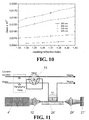
- the difference between the derivatives is especially significant, and subsequently the sensitivity is higher, in thin waveguides. For example, in a 300 nm thick waveguide, sensitivity can be three times higher than in a 470 nm thick waveguide.
- the sensitivity expressed in terms of phase shift per unit of refractive index can be obtained from figure 9 and expression (3).
- a phase change of 2 ⁇ can be reached, if the refractive index of the cladding layer changes by 6x10 -4 RIU (Refractive Index Unit), when n cl is around 1.34.
- the sensitivity Sens calculated using expression (4) is plotted versus the refractive index of the cladding layer for four different waveguide thicknesses: ⁇ - 300 nm, ⁇ - 350 nm, ⁇ - 420 nm, ⁇ - 470 nm.
- the sensitivity is the change in the output signal per unit refractive index change in the cladding layer.
- the calculations were performed assuming a 10 mm long waveguide This parameter defines the noise floor which is allowed in the detection circuitry in order to distinguish the changes in the interference pattern. It can be observed that an accuracy of 1% is enough for the readout of the output signal when working with waveguides thinner than 400 nm.
- the sensitivity of the proposed device is comparable to the sensitivity of integrated MZI fabricated by silicon technologies.
- a silicon wafer polished at one side is subject to high temperature oxidation.
- a layer of silicon dioxide of about 2 ⁇ m thick is formed on both sides of the wafer (the side where components are placed, forming the waveguide, and the back side), as a result of this process.
- a layer of silicon nitride of about 400 nm thick is deposited by LPCVD technique on both the components and the back sides.
- a layer of PECVD silicon dioxide is deposited on the front side of the wafer.
- Waveguides are patterned on the front side using conventional photolithography and wet etching in buffered Hydro Fluoridric (HF) acid. Photoresist is removed with oxygen plasma.
- HF Hydro Fluoridric
- the wafer is immersed in HF solution for a time sufficient to remove the silicon dioxide mask and to form simultaneously ribs over the silicon nitride.
- Selective etching is used (the thickness of PECVD oxide is chosen proportional to the rib height).
- the selectivity in etching (silica)/(silicon nitride) is about 1000/14 if the etching is done in a SiO-etch solution (similar to HF10%).
- This technology allows fabrication of rib waveguides with rib height of about 4 nm and width of about 4 ⁇ m.
- the resulting waveguide can support two transversal modes. It is therefore bimodal, having a fundamental mode and a first order mode.
- a layer of silicon oxide is then deposited on the components side as a protection layer.
- a sensing window is formed over a surface of the waveguide using standard photolithography and wet etching in SiO-etch solution.
- a 3 ⁇ m wide waveguide which supported a single mode in lateral direction was used.
- the wafer was diced in chips and the chips were polished to get the end faces of the waveguides polished.
- the chip was mounted on an aluminium base and covered with a polymethylmetacrylate (PMMA) microfluidic header which had a channel in order to provide the reagent flow over the waveguide.
- PMMA polymethylmetacrylate
- the present invention further provides a method for detecting the introduction of changes (e.g. the amount or concentration of a stimulus) in a chemical, biological or physical stimulus of interest in a localised environment.
- the method comprises the following steps carried out in a bimodal optical waveguide interferometer like the one shown in figures 1a, 1b and 1c :
- step (e) further comprises:
- step (f) further comprises:
- the terms “around”, “about”, “approximately” and “substantially” and terms of its family should be understood as indicating values very near to those which accompany the aforementioned term. That is to say, a deviation within reasonable limits from an exact value should be accepted, because the expert in the technique will understand that such a deviation from the values indicated is inevitable due to measurement inaccuracies, etc.
Description
- The present invention relates to interferometers and sensors based on optical waveguides, and more particularly, to interferometers and sensors based on bimodal optical waveguides.
- Detection of a molecule, e.g. protein, glucose or binding between the molecules is a common issue. The amount of reagent or the concentration of the molecules in the solution may be low and highly sensitive devices are required for the detection of the molecules. The detection can be conducted using various methods and techniques. There exists a variety of nanomechanical and optical devices, such as Mach-Zhender interferometers, Surface Plasmon Resonance, Young interferometers, Fabry-Perot interferometers and slab interferometers. Mach-Zhender and Young interferometers are compact devices based on optical waveguides which were introduced long time ago and have been well studied. Today these techniques are considered to be among the most sensitive ones in the field of biomolecular detection, because the simplicity of robust planar structures gives an advantage of relatively simple immobilisation procedures. The developed methods and protocols allow for binding the molecules without labelling. This makes experiments less laborious and more repeatable since labelling was a source of error since it interfered with the actual results. Interferometers have normally two branches, one of which, when the interferometer acts as a sensing device, is provided with a sensing window, the other one being a reference. Reagent flowing through the sensing window interacts with the molecules previously immobilised over the waveguide in the window. This changes the refractive index of the cladding layer of the waveguide and subsequently the velocity of light propagation along this waveguide. As a consequence, there is a phase shift between the light waves propagating in the two branches. Mixing these waves produces different results, depending on the type of interferometer: an interference pattern in the case of the Young interferometer and variation of output channel signal in the case of Mach-Zhender interferometer.
- However, interferometers with two branches have the drawback of having difficulties in accurate splitting the light. If not well fabricated, the critical symmetry of the Y junction leaves the interferometer prone to reduced modulation depth and losses in sensitivity.
- Furthermore, high sensitivity may only be obtained on relatively thin waveguides. Sensitivity is defined by the depth of penetration of the evanescent field of the waveguide into the analyte conjugate to the waveguide, that is to say, into the analyte which is in contact with the waveguide. Penetration depth significantly increases if the waveguide thickness is reduced. This involves difficulties in light coupling due to the mismatch between the intensity distribution of the waveguide propagating mode of thin waveguides and the intensity distribution of a conventional light source.
- What is more, initial phase shift adjustment between the interfering light waves in the two branches requires additional technological and engineering efforts.
- The above mentioned problems can be partially solved by using bimodal waveguide interferometers. An example of a device working with interference of two propagating modes was presented in Japanese patent application
JP2004145246 - The working principle of the structure described in
JP2004145246 Figure 5 shows such a waveguide. Although the physical structure is three-dimensional, from the properties point of view the structure is bidimensional: In longitudinal direction (referred to infigure 5 as X axis) (which is the direction of light propagation), the structure has a step orrib 500 which defines a change in thickness along this longitudinal axis. In transverse direction (referred to infigure 5 as Y axis), the properties (i.e. refractive index) of the waveguide materials change. In lateral direction (referred to infigure 5 as Z axis), the waveguide structure is uniform, because its properties do not change along this lateral direction. The structure is therefore a bidimensional one (from the propagation point of view, it has a longitudinal dimension and a transverse one). - However, the dimensionality of the device of
JP2004145246 - Another example of a device working with interference of propagating modes is presented by G. Coppola et al. in "Temperature Optical Sensor Based on all Silicon Bimodal Waveguide", where the lateral modes are involved in generating the interference pattern. This device can be fabricated using a conventional photolithography.
- Nevertheless, precise control of the interferometer geometry in lateral direction is strongly required for accurate implementation of the device. This control of the lateral geometry of the device is very difficult to achieve using conventional microelectronics technologies.
- What is more, the architecture of the devices in
JP2004145246 and G. Coppola et al. -
US 4940328 A discloses a bimodal waveguide supporting lateral mode, with limited sensitivity. - The present invention exploits bimodal waveguide structures where different relative phase retardation between the two propagating modes accumulates when it is subjected to a structural change. The present invention relates to an optical waveguide interferometer comprising a bimodal waveguide whose propagating modes dispersion is mode order sensitive according to
claim 1. - One aspect of the invention relates to a planar optical waveguide interferometer which comprises a substrate; a bimodal waveguide comprising at least one layer deposited on the substrate, the bimodal waveguide being designed for supporting a zero-order and a first-order transversal propagating modes, the transversal propagating modes having different dispersion; a sensing window located in a selected area of the upper side of the bimodal waveguide, the sensing window being configured for receiving a chemical, biological or physical input stimulus, that stimulus being capable of changing the effective refractive index of the bimodal waveguide. The bimodal waveguide further comprises confining means designed for confining light in lateral direction, the bimodal waveguide being thus designed for supporting one lateral mode.
- The interferometer preferably comprises an electromagnetic radiation source configured for leading optical light into the bimodal waveguide. This source is more preferably a laser.
- Optionally, the source is integrated within the structure of the substrate.
- In a particular embodiment, the interferometer further comprises polarising means.
- Optionally, the interferometer further comprises focussing means. In a particular embodiment, the focussing means is a lens. In this situation, the central axis of the lens is configured to be misaligned in the transversal direction with respect to the longitudinal symmetry axis of the bimodal waveguide, thereby a first and a second transversal propagating modes being excited within the bimodal waveguide when light from a source is directly focussed through said lens towards the bimodal waveguide.
- In a particular embodiment, the interferometer further comprises an input waveguide connected at one end of the bimodal waveguide, this input waveguide being designed for supporting a single mode in both transversal and lateral directions; and an output waveguide connected at the other end of the bimodal waveguide, this output waveguide being designed for supporting a single mode in both transversal and lateral directions. The thickness of each of the input and output waveguides is less than that of the bimodal waveguide, such that due to the non-symmetrical geometry of the structure at the junction of the input waveguide and the bimodal waveguide, the single mode is split into first and second transversal propagating modes. Optionally, the interferometer further comprises means for coupling electromagnetic radiation into the bimodal waveguide, this means being chosen from the group formed by: end-fire, direct focusing, prism coupling and diffraction grating coupling. The amount of light coupled into the output waveguide depends on the intensity distribution at the junction between the bimodal waveguide and the output waveguide.
- In another embodiment, the interferometer further comprises coupling means configured for coupling to the bimodal waveguide first and second order modes of light with different incidence angles. Optionally, the coupling means is a diffraction grating coupled to an input of the bimodal waveguide.
- Preferably, the bimodal waveguide comprises at least two layers. In this case, a first waveguide layer has a first refractive index and a second waveguide layer has a second refractive index. The refractive index of the second layer is lower than that of the first waveguide layer.
- The effective refractive index of the zero-order mode and that of the first-order mode are substantially different. This different dispersion of the transversal propagating modes depends on the propagation velocity on the parameters of the waveguide.
- Optionally, the interferometer further comprises detection means for measuring at the output of the waveguide changes in the radiation intensity due to the input stimulus. In a particular embodiment, the detection means is a two sectional photodetector.
- Another aspect of the invention refers to chip comprising at least one planar optical waveguide interferometer like the above-mentioned one.
- Another aspect of the invention refers to a sensor comprising a planar optical waveguide interferometer like the above-mentioned one.
- Finally, the present invention relates to a sensing method comprising the steps of: (a) defining a sensing window in a selected area of a bimodal waveguide of an optical waveguide interferometer; (b) placing a chemical, biological or physical stimulus in the sensing window; (c) introducing or causing changes in the stimulus; (d) coupling a zero-order mode and a first-order mode of electromagnetic radiation into the bimodal waveguide, in such a way that when both modes travel through the sensing window defined in the bimodal waveguide, they suffer a phase delay which is dependent on the changes in the stimulus; (e) at the output of the bimodal waveguide, measuring the response of the zero-order mode relative to the response of the first-order mode; and (f) relating that relative response of both modes to the changes in the stimulus.
- Preferably, the step of measuring the response of the zero-order mode relative to that of the first-order mode further comprises: generating a pattern of interference fringes; and measuring a displacement in the interference pattern. Furthermore, the step of relating the relative response of both modes to the changes in the stimulus further comprises relating the displacement in the interference pattern to the presence of changes in the stimulus of interest.
- The advantages of the proposed invention will become apparent in the description that follows.
- To complete the description and in order to provide for a better understanding of the invention, a set of drawings is provided. Said drawings form an integral part of the description and illustrate a preferred embodiment of the invention, which should not be interpreted as restricting the scope of the invention, but just as an example of how the invention can be embodied. The drawings comprise the following figures:
-
Figures 1a-1c are schematic representations of optical waveguide interferometers according to the present invention. -
Figure 1d represents an example of the intensity distribution of the propagating modes in the transversal direction in an optical waveguide interferometer according to the present invention. -
Figure 2a illustrates an example of an interferometer and sensor according to the present invention. -
Figure 2b shows an implementation of the example offigure 2a . -
Figure 3 illustrates an example of an interferometer and sensor according to the present invention. -
Figure 4 illustrates an example of an interferometer and sensor according to the present invention. -
Figure 5 shows a prior art bidimensional planar waveguide. -
Figures 6 and 7 illustrate a waveguide wherein the meaning of "transverse" and "lateral" according to the present invention is explained. -
Figure 8 shows two simulations of the signals detected at the output of an interferometer of the invention. -
Figure 9 shows a simulation which represents how the refractive index of the cladding layer affects the propagation constants of the two modes according to the invention. -
Figure 10 represents the sensitivity versus the refractive index of the cladding layer according to the invention. -
Figure 11 shows a schematic view of an experimental set-up of a sensor according to the invention. -
Figures 12a and 12b show the response of the sensor offigure 11 under different conditions. - In the context of the present invention, the following definitions must be considered:
- As illustrated in
figure 6 , a "transverse mode" of a light beam of electromagnetic radiation is a particular intensity pattern of radiation measured along a line formed by a plane (plane 1 or plane YOZ) perpendicular to the propagation direction of light beam and a plane (plane 2 or plane XOY) perpendicular to a waveguide structure and going along the propagation direction. In the context of the present invention, the term "vertical" is to be considered as a synonym of "transverse". - As illustrated in
figure 7 , a "lateral mode" of a light beam of electromagnetic radiation is a particular intensity pattern of radiation measured along a line formed by a plane (plane 1 or plane YOZ) perpendicular to the propagation direction of light beam and the plane (plane 3 or plane XOZ) in which a waveguide structure lies, and going along the propagation direction. In the context of the present invention, the term "horizontal" is to be considered as a synonym of "lateral". - The transverse and lateral modes can be classified into TE (transverse electric) modes and TM (transverse magnetic) modes. TE modes are those which have no electric field in the direction of propagation, while TM modes are those which have no magnetic field in the direction of propagation.
- The "dispersion" of a waveguide mode is a dependence of the propagation velocity of said mode on the parameters of the waveguide and its surrounding layers.
- "Analyte" is any solution containing a substance which is to be detected by the interferometer and sensor of the present invention.
- The implementation of the present invention can be carried out as follows:
-
Figure 1a shows a schematic representation of a singleoptical waveguide 10 which supports two modes of the present invention. The two modes thewaveguide 10 is capable of supporting are transversal modes (TE or TM): a fundamental TE or TM mode and a first order TE or TM mode. Although two lateral modes could be chosen, in order to overcome the already mentioned disadvantages derived from structures confining two lateral modes, a structure configured to confine two transversal modes is chosen and designed. - This
optical waveguide 10 acts as an interferometer. Theoptical waveguide 10 comprises at least onelayer 2 of optically transparent material deposited in a laminar fashion onto asubstrate 8. Preferably, thewaveguide 10 comprisesseveral layers 1 2 3 of optically transparent material deposited in a laminar fashion onto asubstrate 8.Layer 2 is of higher refractive index than that ofadjacent layers 1 3. Therefore, in this case theoptical waveguide 10 is an optical slab waveguide. Thewaveguide 10 can have a single layer: Onelayer 1 over the substrate is enough, because, as will be explained later, an analyte deposited over the upper layer (which can be the only layer) also forms a layer (a covering layer) above thewaveguide 10. Thus, the working principle of the interferometer according to which light travels over a structure with areas having different refractive index is fulfilled, said two areas being the monolayer waveguide 10 (supported on a substrate 8) and the analyte or covering layer deposited thereon. Preferably, a plurality oflayers 1 2 3 are used in order to optimise the structure. -
Waveguide 10 further comprises confiningmeans 9 which are capable of confining light in lateral direction. Thanks to this confining means 9, thewaveguide 10 can support at least one lateral mode. - It is remarked that, in an ideal situation with a perfect waveguide, wherein confinement in transversal direction is provided, a light beam with relatively wide lateral distribution (about 1mm for example) would propagate substantially without divergence. This means that after propagating transversally for several millimetres, the light beam would maintain the same width for about 1 mm. In this case no rib or ridge would be required. However, wide beams make the waveguide bulky and impractical in the sense of integration of many waveguides in an array on the same chip. Turning to narrow light beams (having width of less than about 100 µm), light inside such waveguides gets very divergent, which means that after propagation transversally for several millimetres, the light beam diverges and expands several millimetres in lateral direction. This makes the device impractical. In other words, in practice, single mode operation in lateral direction is extremely difficult to maintain in a simple, planar structure is used. What is more, the longer the waveguide is, the more difficult it is to maintain single mode operation in lateral direction. For this reason, confining means such as ribs, ridges, etc. are necessary.
- Single mode operation in lateral direction also facilitates the modelling of the interferometer when working as a sensor and makes predictable its behaviour.
- Non-limiting examples of confining
means 9 which can provide such confinement are a rib, a ridge or a gradient. Appropriate waveguides are therefore: rib, ridge, gradient or other waveguide structures.Waveguide 10 therefore permits propagation of incident electromagnetic radiation in the direction represented by the length of thewaveguide 10, that is to say, in the direction represented by the arrow which comes out ofoptical source 4. Thewaveguide 10 is preferably a rectangular waveguide, so that the modes are laterally and transversally confined. The fact that the waveguide is rectangular does not mean that in the plane perpendicular to the propagation direction the waveguide has necessarily rectangular profile. On the contrary, the waveguide cross section may have a small step, forming a rib waveguide structure. - In a particular embodiment,
waveguide 10 is a rib waveguide. This is illustrated infigure 1a , wherein thewaveguide 10 comprises arib 9 in the lateral direction (according to the scheme offigure 5 ). Thisrib 9 implies that the thickness of thewaveguide 10 varies along said lateral direction.Figure 1b shows another view of thesame waveguide 10 having arib 9.Reference 19 infigure 1c represents another type ofwaveguide 10. Infigure 1b , the three propagation directions are illustrated: longitudinal, X, direction (which is the direction of light propagation), transversal direction, Y, and lateral direction, Z. - As can be appreciated, the structure of the present invention is homogeneous in the direction of light propagation (longitudinal direction), while the structure disclosed in
JP2004145246 - Although not illustrated in
figures 1c-1c , the structure also comprises a sensing window or area which is formed over a surface of the waveguide using standard photolithography and wet etching. This sensing window is illustrated infigures 2 to 4 . - One of the advantages of this 2D structure is that the waveguide confines single mode light (thus is able to propagate light) for several centimetres without light divergence in lateral direction. Single mode operation in lateral direction is required because of the following reasons: First, when the waveguide is used as an interferometer or as a sensor, it helps to avoid ambiguities in monitoring the interference pattern created at the waveguide end. Second, narrow waveguides, which can only be implemented by two dimensional structures (i.e. ribs, ridges, etc.) allow squeezing the sensing area to a fraction of square millimetre. The sensing area can vary from about 0.05 to about 1 mm2. As a matter of example, a 15 mm long and 0.01 mm wide waveguide has an area of 0.15 mm2.
- Sensitivity is very important in the device of the present invention. The structure needs to be long enough in order to work as a waveguide interferometer, because its sensitivity is proportional to the length of the sensing window or area or to the length of the bimodal waveguide. Thus, the length of the structure is preferably in the following range: between around 0.5 and around 5 cm.
-
Figure 1c shows how thewaveguide 10 formed by an implanted waveguide may be fabricated by implantation.Reference 18 represents an area whereinwaveguide 19 is implanted. The refractive index changes over thisarea 18. Such a waveguide has spatial change in index of refraction in transversal and lateral directions, while geometrically it keeps being a plane slab structure. - Light from a
source 4 may be transmitted to theinput end 5 of thewaveguide 10 so as to illuminatelayer 2. Preferably, thelight source 4 provides light having a wavelength falling within the visible or near infrared range, such as between around 400 and around 1600 nm.Light source 4 is preferably a laser source. - The two transversal propagating modes are thus equally excited and travel through the length of the
waveguide 10, accumulating different phase delay. At theoutput end 6 ofwaveguide 10, light can radiate from the end surface onto a screen or measuringdevice 7. The intensity distribution represents the accumulated relative phase delay. Non-limiting examples of measuringdevices 7 are detectors, such as one or more photodiodes. Where more than one photodetector is used, they are arranged in an array, such as a two-dimensional photodiode array or a CCD camera. - The elements already described and illustrated in
figure 1a form a planaroptical waveguide interferometer 15. - The two transversal modes are capable of exhibiting a measurable relative response to a change in the wavelength of incident electromagnetic radiation or in a localised environment. If the refractive index of
layer 1 locally changes, a different relative phase delay accumulates and the intensity distribution is modified accordingly. Optical waveguide transversal modes have an electric field that is distributed among thelayers 1 2 3 and in some cases through thesubstrate 8 of thewaveguide structure 10. The relative amount of power contained in thelayers 1 2 3 determines the "effective refractive index" of the waveguide mode. In turn, the effective refractive index of a mode determines the propagation speed of that mode and therefore the extent of phase delay that can be accumulated as the mode travels through thewaveguide 10. If the refractive index of alayer 1 2 3 changes, the field distribution also changes, thereby resulting in a change in the effective refractive index. If the dispersion properties of the modes are different, then the change in effective refractive index can be quite large. The propagation constants for the fundamental and the first order modes depend on the refractive index of the upper or covering layer. As already mentioned, when theoptical waveguide 10 works as an interferometer, and an analyte is deposited over theupper layer 1, the analyte works as a covering layer. In other words, it is necessary that the dispersion (that is to say, the dependence of the propagation constants on the refractive index) is different for each mode. The interference pattern of the two modes at the end of the waveguide is dependent on the refractive index of the conjugate layers, and therefore on the analyte solution refractive index. -
Figure 1d represents an example of the intensity distribution of the propagating modes in the transversal direction. The distance in transversal direction is indicated in X axis in nm. The normalised intensity of the electric field is indicated in the Y axis (the magnitude not being so important as the actual response or shape). Infigure 1d ,reference 11 represents a distribution of intensity of the fundamental mode.References figure 1d , the dispersion effect is due to the markedly different power distribution between both modes. - The
optical waveguide structure 10 forming an optical interferometer may be advantageously manufactured using any suitable combination of conventional materials. Examples of conventional methods of fabrication are those based on Chemical Vapor Deposition (CVD), such as Plasma Enhancement Chemical Vapor Deposition (PECVD) or Low Pressure Chemical Vapor Deposition (LPCVD). - Chemical Vapor Deposition (CVD) is a chemical process used to produce high-purity, high-performance solid materials, such as thin films. In a typical CVD process, the wafer (substrate) is exposed to one or more volatile precursors, which react and/or decompose on the substrate surface to produce the desired deposit. Microfabrication processes widely use CVD to deposit materials in various forms, including: monocrystalline, polycrystalline, amorphous and epitaxial. These materials include: silicon, carbon fiber, filaments, carbon nanotubes, SiO2, silicon-germanium, tungsten, silicon carbide, silicon nitride, silicon oxynitride, titanium nitride, and various high-k dielectrics.
- For example, the refractive index of a silicon oxynitride optical waveguide of constant thickness (typically in the range of 0.3-0.5 microns) may be selected at any level in the range of 1.457 to 2.00.
- Preferably, the first waveguide mode and second waveguide mode are capable of exhibiting a measurable relative response to a change in a localised environment caused by the introduction of changes in a physical, biological and/or chemical stimulus of interest. This response is caused by the evanescent field of the modes as they extend into the localised environment. An example of introduction of a change in a stimulus is a change in the refractive index of the material (i.e. analyte) placed in that environment. As a consequence of that change, the first and second waveguide modes accumulate different relative phase delay, thereby causing a measurable relative response.
- This means that the planar
optical waveguide interferometer 15 can advantageously be used to detect the presence of changes in a physical, biological and/or chemical stimulus in an analyte introduced into the localised environment. The optical waveguide interferometer thus becomes a chemical sensor waveguide interferometer or a sensor based on optical waveguide. Non-limiting examples of interaction of the stimulus with the waveguide modes are: binding interaction, absorbance interaction or any other interaction. For example, a gaseous or liquid phase analyte comprising chemical stimuli may be introduced into the localised environment of the optical waveguide interferometer. Alternatively, a chemical reaction may take place in said environment, causing changes in the nature of the chemical stimuli in situ, thereby causing a change in the localised environment. - The localised environment, also called sensing layer or sensing window, is preferably an area or surface of the
upper layer 1 of the optical waveguide 10 (not illustrated infigures 1a-1c ). This sensing layer may comprise a material chosen from the following group: absorbent materials and bioactive materials. Non-limiting examples of absorbent materials are polymeric materials, such as a polysiloxane or imprinted polymers. An absorbent material is capable of absorbing gases, liquids or vapours comprising a chemical stimulus of interest. Non-limiting examples of bioactive materials are those comprising monoclonal and polyclonal antibodies, enzymes, DNA fragments, RNA, aptamers, PNAs, functional proteins or whole cells. A bioactive material may be appropriate for liquid or gas phase biosensing. - An interference pattern is generated inside the bimodal waveguide 10 (acting as an interferometer) when electromagnetic radiation propagates along the
waveguide 10. The above mentioned changes in a stimulus in a localised environment or sensing layer, or a change in wavelength, may be calculated from the relative phase shift of the interference pattern. The measurable response to said change is represented by a displacement of the fringes in the interference pattern. The relative phase shift of the radiation within the interferometer may be calculated by measuring said displacement in the fringes. At theoutput 6 of thewaveguide 10, the electromagnetic radiation is coupled into free space. The interference pattern can thus be recorded in a conventional manner (such as using asingle detector 7 which measures the changes in the radiation intensity or using a plurality ofsuch detectors 7 which monitor the changes occurring in a number of fringes or in the entire interference pattern).Such detectors 7 are preferably one or more photodetectors. Where more than one photodetector is used, they are arranged in an array, such as a two-dimensional photodiode array. - As shown in
figure 1a , light from asource 4 is focussed to theinput end 5 of thewaveguide 10 and propagated in the form of electromagnetic radiation, which can be coupled into the first and second waveguide modes in different ways. - In one particular embodiment, radiation is simply coupled into the
waveguide 10 via anend face 5 of saidwaveguide 10. This is also called "an end firing procedure". In this case, the light source (i.e. laser) is integrated with thelaminate structure 1 2 3 on thecommon substrate 8. Non-limiting examples ofsubstrates 8 are silicon and indium phosphide substrates. - Alternatively, the
interferometer 15 comprises other coupling means for coupling the incident electromagnetic radiation into the first (fundamental) and second (first-order) waveguide modes of thewaveguide 10. This coupling of the two modes is done substantially simultaneously. Non-limiting examples of coupling means, apart from end-fire, are direct focusing (for example, by means of a HeNe laser), prism coupling, diffraction grating coupling or mirror coupling. - Optionally, the incident light or electromagnetic radiation may be oriented (e.g. plane polarised) as desired using appropriate polarising means. Non-limiting examples of polarising means are polarising cube beam splitters, linear glass polarisers and wire grid polarisers.
- Optionally, the incident light or electromagnetic radiation may be focussed using focussing means. Non-limiting examples of focussing means are: a lens, a microlens and an optical system comprising a series of lenses.
- Optionally, the output electromagnetic radiation pattern may be projected towards the above mentioned detector by means of projecting means. Non-limiting examples of projecting means are objective lenses, lenses and direct projection onto multi sectional photodetector.
- Next, some examples of interferometers based on bimodal waveguides and sensors based on interferometers are described:
-
Figure 2 illustrates an example ofinterferometer 25 which comprises abimodal waveguide 20, formed by one or more layers as illustrated infigures 1a, 1b and1c . On its upper surface, thewaveguide 20 comprises asensing window 21, wherein an analyte can be deposited. Waveguide modes (the fundamental and the first order ones) are excited in thewaveguide 20 using direct focusing of light from a laser source (not shown infigure 2 ) by means of anobjective lens 22. A structure is considered non-symmetrical in transverse direction if the distribution of the refractive index across the structure in transversal direction is not symmetrical with respect to the symmetry axis of the structure. The symmetry axis of the structure is an axis going in the direction of light propagation and crossing the plane perpendicular to the light propagation direction in a point where maximum intensity of electromagnetic field distribution of a transverse fundamental mode is located. The structure offigure 5 is thus non-symmetrical. Because the structure is not symmetrical and the central axis of theobjective lens 22 can be misaligned in the transversal direction with respect to the symmetry axis of the waveguide layer, both the zero (fundamental) and the first order modes are excited. The two transversal modes propagate with different velocities and pass by thesensing window 21. The interference pattern formed at theoutput end 16 of thewaveguide 20 is projected on a two sectional photodetector (TSP) 27 using anobjective lens 29 as a projecting and magnifying means. The position of the maximum of the interference pattern is defined, among other parameters, such as the refractive index, the thickness of each layer, the length of the waveguide and the width of the waveguide, by the initial phase of the excited waves and by the refractive index of the analyte passing through thesensing window 21. It is thus registered the change in the refractive index of the covering layer (measured in the sensing window) caused by a chemical or biological reaction which has occurred on the waveguide surface or by changes in the analyte solution. -
Blocks 28 refer to the walls of a microfluidic cell which can be attached to thewaveguide 20 in order to provide flow and exchange of the analyte. They are not part of the present invention. -
Figure 2b shows an implementation of the example offigure 2a . The interference pattern in the transversal direction can be distributed with the maximum located in the lower or in the upper part of the waveguide, as shown infigure 2b , where the distributions of light intensities in the waveguide cross section are shown in the inset. The distributions are built for a waveguide with refractive index of 2.0 (silicon nitride) and with thickness of 400 nm. The phase difference between the modes varies by π radian from one curve to the other. Under certain conditions the difference between the energies concentrated in the top and in the bottom sections of the photodetector can reach -17 dB. The output intensity is proportional to the amount of light coupled into the waveguide at the input. If absorption over the waveguide is constant, then the total light power at the exit is proportional to the power coupled at the input except for some changes due to reflectivity from the output facet, which according to simulations is slightly changing with the interference pattern movement. Assuming that the function of the reflectivity change is known, the ambiguities due to coupling efficiency variations can be reduced, because monitoring with a two sectional photodetector (TSP) allows to register simultaneously both the total power and the shift in the distribution of light exiting the bimodal waveguide (BiMW). -
Figure 3 illustrates an example ofinterferometer 35 which comprises abimodal waveguide 30, formed by one or more layers as illustrated infigures 1a, 1b and1c . On its upper surface, thebimodal waveguide 30 comprises asensing window 31 wherein an analyte can be deposited. Theinterferometer 35 comprises, at both ends of saidbimodal waveguide 30,single mode waveguides 31 32. Bothinput waveguide 31 andoutput waveguide 32 are single mode in transversal and lateral directions. The only parameter which varies from thesingle mode part 31 32 to thebimodal part 30 is the thickness. This implies that the thickness of these twowaveguides 31 32 is less than the thickness of thebimodal waveguide 30. Light is coupled into theinput waveguide 32 by any conventional coupling means, such as end-fire, direct focusing, prism coupling or diffraction grating coupling. The particular coupling means used in theinterferometer 35 offigure 3 is direct coupling by means of a focussinglens 34. Because the structure is not symmetrical at the junction input waveguide 32 -bimodal waveguide 30, the fundamental mode (which is the only mode which propagates through the input waveguide 32) splits into two modes: the fundamental and the first order ones, in thebimodal waveguide 30. The ratio between the modes amplitudes is defined by the geometry of the structure or, more precisely, by the thickness of thewaveguides 32 30 31. Optimisation of the wavelength thickness is an engineering problem which can be solved on the basis of conventional modelling methods. The amount of light coupled into theoutput waveguide 33 depends on the intensity distribution at the junction bimodal waveguide 30 -output waveguide 33. In this example, the readout of the output signal coming out of theoutput waveguide 33 is performed by aconventional photodetector 37, such as a photodiode. The output interference pattern is projected on saidphotodetector 37 using anobjective lens 39 as a projecting means. -
Figure 4 illustrates an example ofinterferometer 45 which comprises abimodal waveguide 40 deposited on asubstrate 48. On its upper surface, thebimodal waveguide 40 comprises asensing window 41 wherein an analyte can be deposited. Light is coupled into thebimodal waveguide 40 by means of adiffraction grating coupler 42 mounted or integrated on thebimodal waveguide 40. The fundamental and the first order modes are excited by light beams (i.e. laser beams) coming from a single source (not illustrated infigure 4 ) and directed to thediffraction grating coupler 42 at different incidence angles θ0 θ1 corresponding to the phase match condition for each mode. Both modes are diffracted bydiffraction grating coupler 42 and propagate through thebimodal waveguide 40. - As already mentioned, sensitivity is proportional to the length of the sensing window or to the length of the bimodal waveguide. Next, an analysis of the sensitivity of the device of
figure 2b is done. - Using the transfer matrix approach, the distributions of light intensities for each mode of a waveguide with index of refraction 2.0 (silicon nitride) on a silica substrate (index of refraction 1.46) and variable refractive index of cladding layer are built. Then, the distributions of the interference pattern at the waveguide exit and the corresponding signals generated by the photodetector sections are calculated as a function of the phase shift between the modes. The signals produced by the photodetector sections are recalculated into a relative change, S r, of the output signal according to the expression:

where Uup, Udown are the signals generated by the upper and the lower sections of the photodetector respectively. The results of the simulations (Sr versus the phase shift) are presented infigure 8 . All calculations were performed for a wavelength of 632.8 nm. The amplitudes of the modes were previously normalised to unity. The curve built for the 400 nm thick waveguide (solid line) is a little more steep than that for 300 nm thick waveguide (dash line). The reason is non symmetrical distribution of the waveguide modes which is getting stronger for the thin waveguides. However, the difference between the curves slopes is not that remarkable: 4/π for the waveguide with thickness of 300 nm and 4.3/π for the 400 nm thick waveguide. - Considering a uniform bimodal waveguide with the modes propagating over a distance L until the exit of the waveguide, the sensitivity of the device, defined as a change in the output signal per cladding refractive index change, can be expressed by the formula:

where ncl is the refractive index of the cladding layer, and ϕ is the phase difference between the modes. - The phase difference due to a change in the refractive index of the cladding layer after a certain distance L is:

where L is the length of the sensing window, λ is the wavelength,


- The refractive index of the cladding layer differently affects the propagation constants


figure 9 as a function of the refractive index of the cladding layer. Dash lines correspond to the fundamental mode, solid lines correspond to the first mode. The waveguide thickness corresponds to: □ - 300 nm, ○ - 350 nm, △ - 420 nm, ∇ - 470 nm. Obviously, the deeper the waveguide modes penetrate into the cladding, the more effective refractive index modulation for the both modes. The penetration of the modes is inverse proportional to the waveguide thickness and proportional to ncl. The derivatives shown infigure 9 for both modes are increasing with the increase in the refractive index of the cladding layer. However, the propagation constant of the first order mode is strongly affected by the cladding refractive index changes. The difference between the derivatives is especially significant, and subsequently the sensitivity is higher, in thin waveguides. For example, in a 300 nm thick waveguide, sensitivity can be three times higher than in a 470 nm thick waveguide. - The sensitivity expressed in terms of phase shift per unit of refractive index can be obtained from
figure 9 and expression (3). Thus, on a 300 nm thick and 10 mm long waveguide, a phase change of 2π can be reached, if the refractive index of the cladding layer changes by 6x10⁻⁴ RIU (Refractive Index Unit), when ncl is around 1.34. - In
figure 10 the sensitivity Sens calculated using expression (4) is plotted versus the refractive index of the cladding layer for four different waveguide thicknesses: □ - 300 nm, ○ - 350 nm, △ - 420 nm, ∇ - 470 nm. The sensitivity is the change in the output signal per unit refractive index change in the cladding layer. The calculations were performed assuming a 10 mm long waveguide This parameter defines the noise floor which is allowed in the detection circuitry in order to distinguish the changes in the interference pattern. It can be observed that an accuracy of 1% is enough for the readout of the output signal when working with waveguides thinner than 400 nm. The sensitivity of the proposed device is comparable to the sensitivity of integrated MZI fabricated by silicon technologies. - Next an example of fabrication is provided: A silicon wafer polished at one side is subject to high temperature oxidation. A layer of silicon dioxide of about 2 µm thick is formed on both sides of the wafer (the side where components are placed, forming the waveguide, and the back side), as a result of this process. A layer of silicon nitride of about 400 nm thick is deposited by LPCVD technique on both the components and the back sides. A layer of PECVD silicon dioxide is deposited on the front side of the wafer. Waveguides are patterned on the front side using conventional photolithography and wet etching in buffered Hydro Fluoridric (HF) acid. Photoresist is removed with oxygen plasma. The wafer is immersed in HF solution for a time sufficient to remove the silicon dioxide mask and to form simultaneously ribs over the silicon nitride. Selective etching is used (the thickness of PECVD oxide is chosen proportional to the rib height). The selectivity in etching (silica)/(silicon nitride) is about 1000/14 if the etching is done in a SiO-etch solution (similar to HF10%). This technology allows fabrication of rib waveguides with rib height of about 4 nm and width of about 4 µm. The resulting waveguide can support two transversal modes. It is therefore bimodal, having a fundamental mode and a first order mode. A layer of silicon oxide is then deposited on the components side as a protection layer. A sensing window is formed over a surface of the waveguide using standard photolithography and wet etching in SiO-etch solution.
- For the current experiment a 3 µm wide waveguide which supported a single mode in lateral direction was used. The wafer was diced in chips and the chips were polished to get the end faces of the waveguides polished. The chip was mounted on an aluminium base and covered with a polymethylmetacrylate (PMMA) microfluidic header which had a channel in order to provide the reagent flow over the waveguide. The length of the sensing window L was 3 mm.
- Next a biosensor based on a bimodal optical waveguide according to the invention is described. Experiments on the detection of the reagent refractive index changes were done by injecting water:glycerine solution into the channel. The schematic view of the experimental set-up is presented in
figure 11 . The flow was provided by a peristaltic pump. Light was launched into the waveguide 20' through anobjective lens 52 focusing a beam from a He-Ne laser 4'. In this case, the laser is a HeNe Laser of 10 mW, which also comprises a beam expander. Slight misalignment of the objective with respect to the waveguide in vertical direction allows for excitation of both modes simultaneously. Light was collected by another objective lens 29' and the image of the waveguide facet was projected on to the TSP 27'. The signal was stabilised while DI water was passing by thesensing window 51.Valve 53 is used for directing a flow with or without reagent to a channel passing in the microfluidic cell by thesensing window 51. Then solutions with three different concentrations, with indexes of refraction 1.3356, 1.337, and 1.39, were injected into the channel. Infigures 12a and 12b the time diagrams of the output signal are presented. The experiments were carried out on two different samples and at different time, so the modulation amplitudes and sensitivities varied from one experiment to another. Injection of highly concentrated solution of glycerine (44 % vol. and refractive index of 1.39) caused a strong phase change and 18π oscillations (seefigure 12a ). Injection of low concentrated solution of glycerine (2.2% or 3.3% vol. with corresponding refractive indexes of 1.3356 and 1.337, correspondingly) resulted in a weak phase changes and almost π and 2π oscillations, respectively (seefigure 12b ). - Analysing the results of the experiments and assuming the refractive index of DI water of 1.333, a phase change of about 2π radian per 0.006 cladding RIU change was observed. The curve slope at the most sensitive position is around 0.06 per 10-4 RIU. Subsequently in order to detect index variation of 10-6 RIU an accuracy of 6x10⁻⁴ (0.06%) in measuring the absolute value of the output signal is required. Stability of the output signal must be of the same order of magnitude. Assuming the sensing window to be 10 mm long, the sensitivity is 0.002 per 10-6 RIU change. Although there are some discrepancies between the theoretically predicted sensitivities and the experimentally demonstrated ones, they are due to the coupling technique used in the experiment, which can not always guaranty the appropriate amplitude ratio between the excited modes. In other words, this discrepancy is a consequence of engineering limitations.
- The present invention further provides a method for detecting the introduction of changes (e.g. the amount or concentration of a stimulus) in a chemical, biological or physical stimulus of interest in a localised environment. The method comprises the following steps carried out in a bimodal optical waveguide interferometer like the one shown in
figures 1a, 1b and1c : - (a) defining a
sensing window 21 31 41 in a selected area of the upper side of thewaveguide 10 20 30 40; - (b) placing a chemical, biological or physical stimulus or analyte in said
sensing window 21 31 41; - (c) introducing or causing changes in said chemical, biological or physical stimulus in said
sensing window 21 31 41; - (d) coupling a fundamental mode and a first-order mode of electromagnetic radiation into said
optical waveguide 10 20 30 40, in such a way that when both modes travel through thesensing window 21 31 41 defined in the waveguide, they suffer a variation in its characteristics, such as a phase delay, which is dependent on the changes in said chemical, biological or physical stimulus; - (e) at the output of said waveguide, measuring the response of said fundamental mode relative to the response of said first-order mode; and
- (f) relating said relative response of both modes to the changes in the chemical, biological or physical stimulus.
- Preferably, step (e) further comprises:
- (e1) generating a pattern of interference fringes; and
- (e2) measuring a displacement in the interference pattern.
- Preferably, step (f) further comprises:
- (f1) relating the displacement in the interference pattern to the presence of changes in the chemical, biological or physical stimulus of interest.
- In conclusion, an interferometer and a biosensor based on a bimodal optical waveguide having a simple design are presented.
- In this text, the term "comprises" and its derivations (such as "comprising", etc.) should not be understood in an excluding sense, that is, these terms should not be interpreted as excluding the possibility that what is described and defined may include further elements, steps, etc.
- In the context of the present invention, the terms "around", "about", "approximately" and "substantially" and terms of its family (such as "approximate", etc.) should be understood as indicating values very near to those which accompany the aforementioned term. That is to say, a deviation within reasonable limits from an exact value should be accepted, because the expert in the technique will understand that such a deviation from the values indicated is inevitable due to measurement inaccuracies, etc.
- On the other hand, the invention is obviously not limited to the specific embodiment(s) described herein, but also encompasses any variations that may be considered by any person skilled in the art (for example, as regards the choice of materials, dimensions, components, configuration, etc.), within the general scope of the invention as defined in the appended claims.
Claims (22)
- Planar optical waveguide interferometer (15, 25, 35, 45) comprising:- a substrate (8, 28, 38, 48);- a bimodal waveguide (10, 20, 20', 30, 40) comprising at least one layer (1, 2, 3) deposited on said substrate (8, 28, 38, 48), said bimodal waveguide (10, 20, 20', 30, 40) being designed for supporting a zero-order and a first-order transversal propagating modes, said transversal propagating modes having different dispersion, wherein said bimodal waveguide (10, 20, 20', 30, 40) further comprises confining means (9) designed for confining light in lateral direction, the bimodal waveguide (10, 20, 20', 30, 40) being thus designed for supporting one lateral mode;- a sensing area (21, 31, 41, 51) located in a selected area of the upper side of said bimodal waveguide (10, 20, 20', 30, 40), said sensing area (21, 31, 41, 51) being configured for receiving a chemical, biological or physical input stimulus, said stimulus being capable of changing the effective refractive index of said bimodal waveguide (10, 20, 20', 30, 40);- detection means (27, 27', 37, 47) for measuring at the output of said waveguide changes in the radiation intensity due to said input stimulus,
characterised in that said detection means is a two sectional photodetector, the interferometer further comprising means adapted to register simultaneously both the total power and the shift in the distribution of light exiting the bimodal waveguide by using said two sectional photodetector. - Planar optical waveguide interferometer (15, 25, 35, 45) according to claim 1, further comprising an electromagnetic radiation source (4, 4') configured for leading optical light into said bimodal waveguide (10, 20, 20', 30, 40).
- Planar optical waveguide interferometer (15, 25, 35, 45) according to claim 2, wherein said electromagnetic radiation source (4, 4') is a laser.
- Planar optical waveguide interferometer (15, 25, 35, 45) according to claim 2, wherein said electromagnetic radiation source is integrated within the structure of the substrate (8, 28, 38, 48).
- Planar optical waveguide interferometer (15, 25, 35, 45) according to any preceding claim, further comprising polarising means.
- Planar optical waveguide interferometer (15, 25, 35, 45) according to any preceding claim, further comprising focussing means.
- Planar optical waveguide interferometer (15, 25) according to claim 6, wherein said focussing means is a lens (22, 52).
- Planar optical waveguide interferometer (15, 25) according to claim 7, wherein the central axis of said lens (22, 52) is configured to be misaligned in the transversal direction with respect to the longitudinal symmetry axis of the bimodal waveguide (20, 20'), thereby a first and a second transversal propagating modes being excited within the bimodal waveguide (20), 20' when light from a source is directly focussed through said lens towards the bimodal waveguide (20, 20').
- Planar optical waveguide interferometer (35) according to any claim from 1 to 5, further comprising:- an input waveguide (32) connected at one end of said bimodal waveguide (30), said input waveguide (32) being designed for supporting a single mode in both transversal and lateral directions;- an output waveguide (33) connected at the other end of said bimodal waveguide (30), said output waveguide (33) being designed for supporting a single mode in both transversal and lateral directions;
wherein the thickness of each of said input and output waveguides (32, 33) is less than that of said bimodal waveguide (30), such that due to the non-symmetrical geometry of the structure at the junction of said input waveguide (32) and said bimodal waveguide (30), said single mode is split into said first and second transversal propagating modes. - Planar optical waveguide interferometer (35) according to claim 9, further comprising means for coupling electromagnetic radiation into said bimodal waveguide (30), wherein said means are chosen from the group formed by: end-fire, direct focusing, prism coupling and diffraction grating coupling.
- Planar optical waveguide interferometer (35) according to either claim 9 or 10, wherein the amount of light coupled into the output waveguide (33) depends on the intensity distribution at the junction between the bimodal waveguide (30) and the output waveguide (33).
- Planar optical waveguide interferometer (45) according to any claim from 1 to 5, further comprising coupling means (42) configured for coupling to said bimodal waveguide (40) a zero order mode and a first order mode of light with different incidence angles (θ0, θ1).
- Planar optical waveguide interferometer (45) according to claim 12, wherein said coupling means (42) is a diffraction grating coupled to an input of said bimodal waveguide (40).
- Planar optical waveguide interferometer (15, 25, 35, 45) according to any preceding claim, wherein said bimodal waveguide (10, 20, 20', 30, 40) comprises at least two layers.
- Planar optical waveguide interferometer (15, 25, 35, 45) according to claim 14, wherein a first waveguide layer has a first refractive index and a second waveguide layer has a second refractive index, the refractive index of said second layer being lower than that of said first waveguide layer.
- Planar optical waveguide interferometer (15, 25, 35, 45) according to any preceding claim, wherein the effective refractive index of said zero-order mode and the effective refractive index of said first-order mode are substantially different.
- Planar optical waveguide interferometer (15, 25, 35, 45) according to any preceding claim, wherein said different dispersion of said transversal propagating modes depends on the propagation velocity on the parameters of said waveguide.
- Chip comprising at least one planar optical waveguide interferometer (15, 25, 35, 45) according to any preceding claim.
- Sensor comprising a planar optical waveguide interferometer (15, 25, 35, 45) according to any claim from 1 to 17.
- Sensing method comprising the steps of:(a) defining a sensing area (21, 31, 41, 51) in a selected area of a bimodal waveguide (10, 20, 20', 30, 40) of an optical waveguide interferometer (15, 25, 35, 45);(b) placing a chemical, biological or physical stimulus in said sensing area (21, 31, 41, 51);(c) introducing or causing changes in said chemical, biological or physical stimulus placed in said sensing area (21, 31, 41, 51);(d) coupling a zero-order mode and a first-order mode of electromagnetic radiation into said bimodal waveguide (10, 20, 20', 30, 40), in such a way that when both modes travel through the sensing area (21, 31, 41, 51) defined in the bimodal waveguide (10, 20, 20', 30, 40), they suffer a phase delay which is dependent on the changes in said chemical, biological or physical stimulus;(e) at the output of said bimodal waveguide (10, 20, 20', 30, 40), measuring the response of said zero-order mode relative to the response of said first-order mode; and(f) relating said relative response of both modes to the changes in the chemical, biological or physical stimulus, the method being characterised in that said step of (e) measuring the response of said zero-order mode relative to the response of said first-order mode at the output of said bimodal waveguide (10, 20, 20', 30, 40) is carried out by using a two sectional photodetector (47) to register simultaneously both the total power and the shift in the distribution of light exiting the bimodal waveguide.
- Sensing method according to claim 20, wherein the step of measuring the response of said zero-order mode relative to the response of said first-order mode further comprises:- generating a pattern of interference fringes (11,12,13); and- measuring a displacement in the interference pattern (11,12,13).
- Sensing method according to claim 21, wherein the step of relating said relative response of both modes to the changes in the chemical, biological or physical stimulus further comprises:- relating said displacement in the interference pattern to the presence of changes in the chemical, biological or physical stimulus of interest.
Priority Applications (9)
| Application Number | Priority Date | Filing Date | Title |
|---|---|---|---|
| DK07381053.3T DK2017602T3 (en) | 2007-07-19 | 2007-07-19 | Interferometer and sensor based on bimodal optical waveguide and recording method |
| PL07381053T PL2017602T3 (en) | 2007-07-19 | 2007-07-19 | Interferometer and sensor based on bimodal optical waveguide and sensing method |
| ES07381053.3T ES2465619T3 (en) | 2007-07-19 | 2007-07-19 | Interferometer and sensor based on a bimodal optical waveguide and detection procedure |
| EP07381053.3A EP2017602B1 (en) | 2007-07-19 | 2007-07-19 | Interferometer and sensor based on bimodal optical waveguide and sensing method |
| CA2693423A CA2693423C (en) | 2007-07-19 | 2008-07-18 | Interferometer and sensor based on bimodal optical waveguide and sensing method |
| PCT/ES2008/070142 WO2009010624A1 (en) | 2007-07-19 | 2008-07-18 | Interferometer and sensor based on bimodal optical waveguides, and detection method |
| US12/669,307 US8279445B2 (en) | 2007-07-19 | 2008-07-18 | Interferometer and sensor based on bimodal optical waveguides, and detection method |
| JP2010516528A JP2010533849A (en) | 2007-07-19 | 2008-07-18 | Bimodal optical waveguide based interferometer and sensor and detection method |
| CN2008801062544A CN101842691B (en) | 2007-07-19 | 2008-07-18 | Interferometer and sensor based on bimodal optical waveguides, and detection method |
Applications Claiming Priority (1)
| Application Number | Priority Date | Filing Date | Title |
|---|---|---|---|
| EP07381053.3A EP2017602B1 (en) | 2007-07-19 | 2007-07-19 | Interferometer and sensor based on bimodal optical waveguide and sensing method |
Publications (2)
| Publication Number | Publication Date |
|---|---|
| EP2017602A1 EP2017602A1 (en) | 2009-01-21 |
| EP2017602B1 true EP2017602B1 (en) | 2014-02-26 |
Family
ID=38707226
Family Applications (1)
| Application Number | Title | Priority Date | Filing Date |
|---|---|---|---|
| EP07381053.3A Active EP2017602B1 (en) | 2007-07-19 | 2007-07-19 | Interferometer and sensor based on bimodal optical waveguide and sensing method |
Country Status (9)
| Country | Link |
|---|---|
| US (1) | US8279445B2 (en) |
| EP (1) | EP2017602B1 (en) |
| JP (1) | JP2010533849A (en) |
| CN (1) | CN101842691B (en) |
| CA (1) | CA2693423C (en) |
| DK (1) | DK2017602T3 (en) |
| ES (1) | ES2465619T3 (en) |
| PL (1) | PL2017602T3 (en) |
| WO (1) | WO2009010624A1 (en) |
Cited By (2)
| Publication number | Priority date | Publication date | Assignee | Title |
|---|---|---|---|---|
| WO2018162008A1 (en) | 2017-03-10 | 2018-09-13 | Leibniz-Institut Für Photonische Technologien E.V. | Assembly and method for detecting changes to the optical path length in a nano capillary channel |
| US10816550B2 (en) | 2012-10-15 | 2020-10-27 | Nanocellect Biomedical, Inc. | Systems, apparatus, and methods for sorting particles |
Families Citing this family (21)
| Publication number | Priority date | Publication date | Assignee | Title |
|---|---|---|---|---|
| EP2351601B1 (en) * | 2008-10-16 | 2016-05-25 | Hatsuta Seisakusho Co., Ltd. | Fire extinguisher, storage container for fire-extinguishing agent, and preform of storage container for fire-extinguishing agent |
| PL2214049T3 (en) * | 2009-02-03 | 2012-04-30 | Optisense B V | Integrated optical waveguide interferometric sensor |
| BRPI1008861A2 (en) * | 2009-02-04 | 2016-03-15 | Ostendum Holding B V | fluid analysis system |
| US8587490B2 (en) * | 2009-07-27 | 2013-11-19 | New Jersey Institute Of Technology | Localized wave generation via model decomposition of a pulse by a wave launcher |
| GB0921994D0 (en) * | 2009-12-17 | 2010-02-03 | Univ Gent | Methods and systems for optical characterisation |
| EP2801824A3 (en) | 2011-03-30 | 2015-02-25 | Kabushiki Kaisha Toshiba | Measuring system using optical waveguide, measuring device, measuring method, optical waveguide type sensor chip, and magnetic fine particle |
| US9267891B2 (en) * | 2011-06-06 | 2016-02-23 | The Regents Of The University Of California | Multiplex fluorescent particle detection using spatially distributed excitation |
| WO2013056137A1 (en) * | 2011-10-12 | 2013-04-18 | Brown University | Systems and methods enabling high-throughput, real time detection of analytes |
| US20150057949A1 (en) * | 2012-04-19 | 2015-02-26 | Molecular Sensing, Inc. | Event Detection For Back-Scattering Interferometry |
| KR20150003715A (en) * | 2012-04-25 | 2015-01-09 | 휴렛-팩커드 디벨롭먼트 컴퍼니, 엘.피. | Analyzing light by mode interference |
| WO2014110468A1 (en) * | 2013-01-11 | 2014-07-17 | Lumense, Inc. | System and method for sensing ammonia in a fluid |
| US9453791B2 (en) * | 2014-07-01 | 2016-09-27 | Octrolix Bv | Flow cytometry system and method |
| DE102015102454A1 (en) | 2015-02-20 | 2016-08-25 | Osram Opto Semiconductors Gmbh | Method for structuring a nitride layer, structured dielectric layer, optoelectronic component, etching method for etching layers and environmental sensor |
| SE540878C2 (en) * | 2015-06-29 | 2018-12-11 | Briano Floria Ottonello | A sensor device and a method of detecting a component in gas |
| CN105572797B (en) * | 2016-02-15 | 2021-02-26 | 欧阳征标 | Terahertz wave pulse amplitude modulation signal and optical pulse amplitude modulation signal conversion amplifier |
| JP6706814B2 (en) * | 2016-03-30 | 2020-06-10 | パナソニックIpマネジメント株式会社 | Photodetector and photodetection system |
| US10996400B2 (en) * | 2016-08-04 | 2021-05-04 | Mitsubishi Electric Research Laboratories, Inc. | Optical waveguide interferometer |
| US10724139B2 (en) * | 2017-06-19 | 2020-07-28 | Wuhan China Star Optoelectronics Semiconductor Display Technology Co., Ltd. | Encapsulation method for OLED Panel |
| EP3460561A1 (en) | 2017-09-26 | 2019-03-27 | Thomson Licensing | Device for deviating and focusing light |
| US11846574B2 (en) | 2020-10-29 | 2023-12-19 | Hand Held Products, Inc. | Apparatuses, systems, and methods for sample capture and extraction |
| USD987457S1 (en) * | 2021-03-15 | 2023-05-30 | Salvus, Llc | Cartridge |
Citations (1)
| Publication number | Priority date | Publication date | Assignee | Title |
|---|---|---|---|---|
| US5710629A (en) * | 1992-12-10 | 1998-01-20 | Schneider Electric S.A. | Interferometric measuring device forming a spacial interference pattern |
Family Cites Families (12)
| Publication number | Priority date | Publication date | Assignee | Title |
|---|---|---|---|---|
| US4940328A (en) | 1988-11-04 | 1990-07-10 | Georgia Tech Research Corporation | Optical sensing apparatus and method |
| DE59410197D1 (en) * | 1993-03-26 | 2002-11-21 | Hoffmann La Roche | Optical method and device for analyzing substances on sensor surfaces |
| US20020015155A1 (en) * | 1993-09-21 | 2002-02-07 | Ralf-Dieter Pechstedt | Interferometer integrated on silicon-on-insulator chip |
| US5444249A (en) * | 1994-02-14 | 1995-08-22 | Telaire Systems, Inc. | NDIR gas sensor |
| US5623561A (en) * | 1995-09-29 | 1997-04-22 | Georgia Tech Research Corporation | Integrated optic interferometric sensor |
| WO2000026642A1 (en) | 1998-10-30 | 2000-05-11 | Photonic Sensor Systems | Methods and sensors for detecting or measuring an acid or base |
| GB9927249D0 (en) * | 1999-11-18 | 2000-01-12 | Farfield Sensors Ltd | Device |
| US6646747B2 (en) * | 2001-05-17 | 2003-11-11 | Sioptical, Inc. | Interferometer apparatus and associated method |
| EP1415139B1 (en) * | 2001-05-18 | 2013-06-12 | Farfield Group Limited | Method for determining a mass changing event |
| JP2004145246A (en) | 2002-08-29 | 2004-05-20 | Murata Mfg Co Ltd | Plane type two-dimensional waveguide and two-dimensional waveguide type optical device |
| KR100726206B1 (en) | 2006-01-31 | 2007-06-11 | 한국표준과학연구원 | Fiber optic two mode interferometric sensors for the detection of abnormal status and the signal processing method |
| US20080043248A1 (en) * | 2006-08-18 | 2008-02-21 | Meric Ozcan | Photonic crystal sensors using band edge and/or defect mode modulation |
-
2007
- 2007-07-19 DK DK07381053.3T patent/DK2017602T3/en active
- 2007-07-19 ES ES07381053.3T patent/ES2465619T3/en active Active
- 2007-07-19 EP EP07381053.3A patent/EP2017602B1/en active Active
- 2007-07-19 PL PL07381053T patent/PL2017602T3/en unknown
-
2008
- 2008-07-18 JP JP2010516528A patent/JP2010533849A/en active Pending
- 2008-07-18 WO PCT/ES2008/070142 patent/WO2009010624A1/en active Application Filing
- 2008-07-18 US US12/669,307 patent/US8279445B2/en not_active Expired - Fee Related
- 2008-07-18 CA CA2693423A patent/CA2693423C/en active Active
- 2008-07-18 CN CN2008801062544A patent/CN101842691B/en not_active Expired - Fee Related
Patent Citations (1)
| Publication number | Priority date | Publication date | Assignee | Title |
|---|---|---|---|---|
| US5710629A (en) * | 1992-12-10 | 1998-01-20 | Schneider Electric S.A. | Interferometric measuring device forming a spacial interference pattern |
Cited By (3)
| Publication number | Priority date | Publication date | Assignee | Title |
|---|---|---|---|---|
| US10816550B2 (en) | 2012-10-15 | 2020-10-27 | Nanocellect Biomedical, Inc. | Systems, apparatus, and methods for sorting particles |
| WO2018162008A1 (en) | 2017-03-10 | 2018-09-13 | Leibniz-Institut Für Photonische Technologien E.V. | Assembly and method for detecting changes to the optical path length in a nano capillary channel |
| DE102017105113B4 (en) | 2017-03-10 | 2021-09-30 | Leibniz-Institut für Photonische Technologien e.V. (Engl.Leibniz Institute of Photonic Technology) | Arrangement and method for the detection of changes in the optical path length in a nano-capillary channel |
Also Published As
| Publication number | Publication date |
|---|---|
| JP2010533849A (en) | 2010-10-28 |
| US20100271634A1 (en) | 2010-10-28 |
| CN101842691A (en) | 2010-09-22 |
| CA2693423A1 (en) | 2009-01-22 |
| CA2693423C (en) | 2017-10-31 |
| EP2017602A1 (en) | 2009-01-21 |
| PL2017602T3 (en) | 2014-09-30 |
| DK2017602T3 (en) | 2014-06-02 |
| US8279445B2 (en) | 2012-10-02 |
| CN101842691B (en) | 2013-07-03 |
| WO2009010624A1 (en) | 2009-01-22 |
| ES2465619T3 (en) | 2014-06-06 |
Similar Documents
| Publication | Publication Date | Title |
|---|---|---|
| EP2017602B1 (en) | Interferometer and sensor based on bimodal optical waveguide and sensing method | |
| Wangüemert-Pérez et al. | Subwavelength structures for silicon photonics biosensing | |
| US9164026B2 (en) | Packaged chip for multiplexing photonic crystal microcavity coupled waveguide and photonic crystal slot waveguide devices for chip-integrated label-free detection and absorption spectroscopy with high throughput, sensitivity, specificity, and wide dynamic range | |
| US5663790A (en) | Method and apparatus for determination of refractive index | |
| Chrostowski et al. | Silicon photonic resonator sensors and devices | |
| EP0852715B1 (en) | Integrated optic interferometric sensor | |
| US6493090B1 (en) | Detection of a substance by refractive index change | |
| US7447391B2 (en) | Planar-resonator based optical chemo- and biosensor | |
| US7212692B2 (en) | Multiple array surface plasmon resonance biosensor | |
| US10610846B2 (en) | Two-dimensional photonic crystal microarray measurement method and apparatus for highly-sensitive label-free multiple analyte sensing, biosensing, and diagnostic assay | |
| US20090103099A1 (en) | Integrated surface mode biosensor | |
| US9335263B2 (en) | Optical circuit for sensing a biological entity in a fluid and method of configuring the same | |
| JP4118901B2 (en) | Micro instrument | |
| JP2005274329A (en) | Sensor utilizing photonic crystal, and method for detecting substance to be detected | |
| Pham et al. | On-chip bulk-index concentration and direct, label-free protein sensing utilizing an optical grated-waveguide cavity | |
| Zhang et al. | Silicon subwavelength-grating microdisks for optical sensing | |
| Duval et al. | Interferometric waveguide biosensors based on Si-technology for point-of-care diagnostic | |
| Wang et al. | Toward on-chip mid-infrared chem/bio sensors using quantum cascade lasers and substrate-integrated semiconductor waveguides | |
| Okubo et al. | Silicon nitride directional coupler interferometer for surface sensing | |
| Rajasekar et al. | Photonic crystal-based sensors for biosensing applications | |
| US20240061174A1 (en) | Method for generating and interacting with polymeric photonic integrated circuits | |
| Werquin et al. | Silicon Ring Resonator-Based Biochips | |
| Janz et al. | Silicon-based microphotonics for biosensing applications | |
| Janz et al. | Engineering light at the sub-wavelength scale using silicon photonics | |
| Janz et al. | Silicon photonic wire evanescent field sensors: sensor arrays and instrumentation |
Legal Events
| Date | Code | Title | Description |
|---|---|---|---|
| PUAI | Public reference made under article 153(3) epc to a published international application that has entered the european phase |
Free format text: ORIGINAL CODE: 0009012 |
|
| AK | Designated contracting states |
Kind code of ref document: A1 Designated state(s): AT BE BG CH CY CZ DE DK EE ES FI FR GB GR HU IE IS IT LI LT LU LV MC MT NL PL PT RO SE SI SK TR |
|
| AX | Request for extension of the european patent |
Extension state: AL BA HR MK RS |
|
| 17P | Request for examination filed |
Effective date: 20090721 |
|
| 17Q | First examination report despatched |
Effective date: 20090813 |
|
| AKX | Designation fees paid |
Designated state(s): AT BE BG CH CY CZ DE DK EE ES FI FR GB GR HU IE IS IT LI LT LU LV MC MT NL PL PT RO SE SI SK TR |
|
| GRAP | Despatch of communication of intention to grant a patent |
Free format text: ORIGINAL CODE: EPIDOSNIGR1 |
|
| INTG | Intention to grant announced |
Effective date: 20130906 |
|
| GRAS | Grant fee paid |
Free format text: ORIGINAL CODE: EPIDOSNIGR3 |
|
| GRAA | (expected) grant |
Free format text: ORIGINAL CODE: 0009210 |
|
| AK | Designated contracting states |
Kind code of ref document: B1 Designated state(s): AT BE BG CH CY CZ DE DK EE ES FI FR GB GR HU IE IS IT LI LT LU LV MC MT NL PL PT RO SE SI SK TR |
|
| REG | Reference to a national code |
Ref country code: GB Ref legal event code: FG4D |
|
| REG | Reference to a national code |
Ref country code: CH Ref legal event code: EP |
|
| REG | Reference to a national code |
Ref country code: AT Ref legal event code: REF Ref document number: 653873 Country of ref document: AT Kind code of ref document: T Effective date: 20140315 |
|
| REG | Reference to a national code |
Ref country code: IE Ref legal event code: FG4D |
|
| REG | Reference to a national code |
Ref country code: DE Ref legal event code: R096 Ref document number: 602007035193 Country of ref document: DE Effective date: 20140410 |
|
| REG | Reference to a national code |
Ref country code: DK Ref legal event code: T3 Effective date: 20140526 |
|
| REG | Reference to a national code |
Ref country code: NL Ref legal event code: T3 |
|
| REG | Reference to a national code |
Ref country code: ES Ref legal event code: FG2A Ref document number: 2465619 Country of ref document: ES Kind code of ref document: T3 Effective date: 20140606 |
|
| REG | Reference to a national code |
Ref country code: AT Ref legal event code: MK05 Ref document number: 653873 Country of ref document: AT Kind code of ref document: T Effective date: 20140226 |
|
| REG | Reference to a national code |
Ref country code: LT Ref legal event code: MG4D |
|
| PG25 | Lapsed in a contracting state [announced via postgrant information from national office to epo] |
Ref country code: IS Free format text: LAPSE BECAUSE OF FAILURE TO SUBMIT A TRANSLATION OF THE DESCRIPTION OR TO PAY THE FEE WITHIN THE PRESCRIBED TIME-LIMIT Effective date: 20140626 Ref country code: LT Free format text: LAPSE BECAUSE OF FAILURE TO SUBMIT A TRANSLATION OF THE DESCRIPTION OR TO PAY THE FEE WITHIN THE PRESCRIBED TIME-LIMIT Effective date: 20140226 |
|
| REG | Reference to a national code |
Ref country code: CH Ref legal event code: NV Representative=s name: ARNOLD AND SIEDSMA AG, CH |
|
| REG | Reference to a national code |
Ref country code: GR Ref legal event code: EP Ref document number: 20140401000 Country of ref document: GR Effective date: 20140625 |
|
| PG25 | Lapsed in a contracting state [announced via postgrant information from national office to epo] |
Ref country code: SE Free format text: LAPSE BECAUSE OF FAILURE TO SUBMIT A TRANSLATION OF THE DESCRIPTION OR TO PAY THE FEE WITHIN THE PRESCRIBED TIME-LIMIT Effective date: 20140226 Ref country code: AT Free format text: LAPSE BECAUSE OF FAILURE TO SUBMIT A TRANSLATION OF THE DESCRIPTION OR TO PAY THE FEE WITHIN THE PRESCRIBED TIME-LIMIT Effective date: 20140226 Ref country code: CY Free format text: LAPSE BECAUSE OF FAILURE TO SUBMIT A TRANSLATION OF THE DESCRIPTION OR TO PAY THE FEE WITHIN THE PRESCRIBED TIME-LIMIT Effective date: 20140226 Ref country code: PT Free format text: LAPSE BECAUSE OF FAILURE TO SUBMIT A TRANSLATION OF THE DESCRIPTION OR TO PAY THE FEE WITHIN THE PRESCRIBED TIME-LIMIT Effective date: 20140626 |
|
| PG25 | Lapsed in a contracting state [announced via postgrant information from national office to epo] |
Ref country code: LV Free format text: LAPSE BECAUSE OF FAILURE TO SUBMIT A TRANSLATION OF THE DESCRIPTION OR TO PAY THE FEE WITHIN THE PRESCRIBED TIME-LIMIT Effective date: 20140226 Ref country code: BE Free format text: LAPSE BECAUSE OF FAILURE TO SUBMIT A TRANSLATION OF THE DESCRIPTION OR TO PAY THE FEE WITHIN THE PRESCRIBED TIME-LIMIT Effective date: 20140226 |
|
| REG | Reference to a national code |
Ref country code: PL Ref legal event code: T3 |
|
| PG25 | Lapsed in a contracting state [announced via postgrant information from national office to epo] |
Ref country code: RO Free format text: LAPSE BECAUSE OF FAILURE TO SUBMIT A TRANSLATION OF THE DESCRIPTION OR TO PAY THE FEE WITHIN THE PRESCRIBED TIME-LIMIT Effective date: 20140226 Ref country code: CZ Free format text: LAPSE BECAUSE OF FAILURE TO SUBMIT A TRANSLATION OF THE DESCRIPTION OR TO PAY THE FEE WITHIN THE PRESCRIBED TIME-LIMIT Effective date: 20140226 Ref country code: EE Free format text: LAPSE BECAUSE OF FAILURE TO SUBMIT A TRANSLATION OF THE DESCRIPTION OR TO PAY THE FEE WITHIN THE PRESCRIBED TIME-LIMIT Effective date: 20140226 |
|
| REG | Reference to a national code |
Ref country code: DE Ref legal event code: R097 Ref document number: 602007035193 Country of ref document: DE |
|
| PG25 | Lapsed in a contracting state [announced via postgrant information from national office to epo] |
Ref country code: SK Free format text: LAPSE BECAUSE OF FAILURE TO SUBMIT A TRANSLATION OF THE DESCRIPTION OR TO PAY THE FEE WITHIN THE PRESCRIBED TIME-LIMIT Effective date: 20140226 |
|
| PLBE | No opposition filed within time limit |
Free format text: ORIGINAL CODE: 0009261 |
|
| STAA | Information on the status of an ep patent application or granted ep patent |
Free format text: STATUS: NO OPPOSITION FILED WITHIN TIME LIMIT |
|
| 26N | No opposition filed |
Effective date: 20141127 |
|
| REG | Reference to a national code |
Ref country code: DE Ref legal event code: R097 Ref document number: 602007035193 Country of ref document: DE Effective date: 20141127 |
|
| REG | Reference to a national code |
Ref country code: IE Ref legal event code: MM4A |
|
| PG25 | Lapsed in a contracting state [announced via postgrant information from national office to epo] |
Ref country code: SI Free format text: LAPSE BECAUSE OF FAILURE TO SUBMIT A TRANSLATION OF THE DESCRIPTION OR TO PAY THE FEE WITHIN THE PRESCRIBED TIME-LIMIT Effective date: 20140226 |
|
| REG | Reference to a national code |
Ref country code: FR Ref legal event code: PLFP Year of fee payment: 9 |
|
| PG25 | Lapsed in a contracting state [announced via postgrant information from national office to epo] |
Ref country code: GR Free format text: LAPSE BECAUSE OF FAILURE TO SUBMIT A TRANSLATION OF THE DESCRIPTION OR TO PAY THE FEE WITHIN THE PRESCRIBED TIME-LIMIT Effective date: 20150505 Ref country code: IE Free format text: LAPSE BECAUSE OF NON-PAYMENT OF DUE FEES Effective date: 20140719 |
|
| PG25 | Lapsed in a contracting state [announced via postgrant information from national office to epo] |
Ref country code: MC Free format text: LAPSE BECAUSE OF FAILURE TO SUBMIT A TRANSLATION OF THE DESCRIPTION OR TO PAY THE FEE WITHIN THE PRESCRIBED TIME-LIMIT Effective date: 20140226 |
|
| PG25 | Lapsed in a contracting state [announced via postgrant information from national office to epo] |
Ref country code: BG Free format text: LAPSE BECAUSE OF FAILURE TO SUBMIT A TRANSLATION OF THE DESCRIPTION OR TO PAY THE FEE WITHIN THE PRESCRIBED TIME-LIMIT Effective date: 20140226 |
|
| PG25 | Lapsed in a contracting state [announced via postgrant information from national office to epo] |
Ref country code: MT Free format text: LAPSE BECAUSE OF FAILURE TO SUBMIT A TRANSLATION OF THE DESCRIPTION OR TO PAY THE FEE WITHIN THE PRESCRIBED TIME-LIMIT Effective date: 20140226 |
|
| REG | Reference to a national code |
Ref country code: FR Ref legal event code: PLFP Year of fee payment: 10 |
|
| PG25 | Lapsed in a contracting state [announced via postgrant information from national office to epo] |
Ref country code: TR Free format text: LAPSE BECAUSE OF FAILURE TO SUBMIT A TRANSLATION OF THE DESCRIPTION OR TO PAY THE FEE WITHIN THE PRESCRIBED TIME-LIMIT Effective date: 20140226 Ref country code: HU Free format text: LAPSE BECAUSE OF FAILURE TO SUBMIT A TRANSLATION OF THE DESCRIPTION OR TO PAY THE FEE WITHIN THE PRESCRIBED TIME-LIMIT; INVALID AB INITIO Effective date: 20070719 |
|
| REG | Reference to a national code |
Ref country code: FR Ref legal event code: PLFP Year of fee payment: 11 |
|
| REG | Reference to a national code |
Ref country code: FR Ref legal event code: PLFP Year of fee payment: 12 |
|
| PGFP | Annual fee paid to national office [announced via postgrant information from national office to epo] |
Ref country code: NL Payment date: 20211025 Year of fee payment: 15 |
|
| PGFP | Annual fee paid to national office [announced via postgrant information from national office to epo] |
Ref country code: LU Payment date: 20211025 Year of fee payment: 15 Ref country code: FI Payment date: 20211021 Year of fee payment: 15 Ref country code: DK Payment date: 20211022 Year of fee payment: 15 |
|
| PGFP | Annual fee paid to national office [announced via postgrant information from national office to epo] |
Ref country code: GR Payment date: 20211025 Year of fee payment: 15 Ref country code: CH Payment date: 20211025 Year of fee payment: 15 |
|
| PGFP | Annual fee paid to national office [announced via postgrant information from national office to epo] |
Ref country code: PL Payment date: 20211014 Year of fee payment: 15 |
|
| PGFP | Annual fee paid to national office [announced via postgrant information from national office to epo] |
Ref country code: IT Payment date: 20220726 Year of fee payment: 16 Ref country code: GB Payment date: 20220728 Year of fee payment: 16 Ref country code: ES Payment date: 20220802 Year of fee payment: 16 Ref country code: DE Payment date: 20220720 Year of fee payment: 16 |
|
| PGFP | Annual fee paid to national office [announced via postgrant information from national office to epo] |
Ref country code: FR Payment date: 20220728 Year of fee payment: 16 |
|
| REG | Reference to a national code |
Ref country code: DK Ref legal event code: EBP Effective date: 20220731 |
|
| REG | Reference to a national code |
Ref country code: CH Ref legal event code: PL |
|
| REG | Reference to a national code |
Ref country code: NL Ref legal event code: MM Effective date: 20220801 |
|
| PG25 | Lapsed in a contracting state [announced via postgrant information from national office to epo] |
Ref country code: LU Free format text: LAPSE BECAUSE OF NON-PAYMENT OF DUE FEES Effective date: 20220719 Ref country code: LI Free format text: LAPSE BECAUSE OF NON-PAYMENT OF DUE FEES Effective date: 20220731 Ref country code: FI Free format text: LAPSE BECAUSE OF NON-PAYMENT OF DUE FEES Effective date: 20220719 Ref country code: CH Free format text: LAPSE BECAUSE OF NON-PAYMENT OF DUE FEES Effective date: 20220731 |
|
| PG25 | Lapsed in a contracting state [announced via postgrant information from national office to epo] |
Ref country code: GR Free format text: LAPSE BECAUSE OF NON-PAYMENT OF DUE FEES Effective date: 20230209 |
|
| PG25 | Lapsed in a contracting state [announced via postgrant information from national office to epo] |
Ref country code: NL Free format text: LAPSE BECAUSE OF NON-PAYMENT OF DUE FEES Effective date: 20220801 |
|
| PG25 | Lapsed in a contracting state [announced via postgrant information from national office to epo] |
Ref country code: DK Free format text: LAPSE BECAUSE OF NON-PAYMENT OF DUE FEES Effective date: 20220731 |
|
| PG25 | Lapsed in a contracting state [announced via postgrant information from national office to epo] |
Ref country code: PL Free format text: LAPSE BECAUSE OF NON-PAYMENT OF DUE FEES Effective date: 20220719 |
|
| REG | Reference to a national code |
Ref country code: DE Ref legal event code: R119 Ref document number: 602007035193 Country of ref document: DE |
|
| GBPC | Gb: european patent ceased through non-payment of renewal fee |
Effective date: 20230719 |