EP2013863B1 - Organic electroluminescent display - Google Patents
Organic electroluminescent display Download PDFInfo
- Publication number
- EP2013863B1 EP2013863B1 EP07728603.7A EP07728603A EP2013863B1 EP 2013863 B1 EP2013863 B1 EP 2013863B1 EP 07728603 A EP07728603 A EP 07728603A EP 2013863 B1 EP2013863 B1 EP 2013863B1
- Authority
- EP
- European Patent Office
- Prior art keywords
- transistor
- voltage
- com
- control
- lines
- Prior art date
- Legal status (The legal status is an assumption and is not a legal conclusion. Google has not performed a legal analysis and makes no representation as to the accuracy of the status listed.)
- Expired - Fee Related
Links
Images


Classifications
-
- G—PHYSICS
- G09—EDUCATION; CRYPTOGRAPHY; DISPLAY; ADVERTISING; SEALS
- G09G—ARRANGEMENTS OR CIRCUITS FOR CONTROL OF INDICATING DEVICES USING STATIC MEANS TO PRESENT VARIABLE INFORMATION
- G09G3/00—Control arrangements or circuits, of interest only in connection with visual indicators other than cathode-ray tubes
- G09G3/20—Control arrangements or circuits, of interest only in connection with visual indicators other than cathode-ray tubes for presentation of an assembly of a number of characters, e.g. a page, by composing the assembly by combination of individual elements arranged in a matrix no fixed position being assigned to or needed to be assigned to the individual characters or partial characters
- G09G3/22—Control arrangements or circuits, of interest only in connection with visual indicators other than cathode-ray tubes for presentation of an assembly of a number of characters, e.g. a page, by composing the assembly by combination of individual elements arranged in a matrix no fixed position being assigned to or needed to be assigned to the individual characters or partial characters using controlled light sources
- G09G3/30—Control arrangements or circuits, of interest only in connection with visual indicators other than cathode-ray tubes for presentation of an assembly of a number of characters, e.g. a page, by composing the assembly by combination of individual elements arranged in a matrix no fixed position being assigned to or needed to be assigned to the individual characters or partial characters using controlled light sources using electroluminescent panels
- G09G3/32—Control arrangements or circuits, of interest only in connection with visual indicators other than cathode-ray tubes for presentation of an assembly of a number of characters, e.g. a page, by composing the assembly by combination of individual elements arranged in a matrix no fixed position being assigned to or needed to be assigned to the individual characters or partial characters using controlled light sources using electroluminescent panels semiconductive, e.g. using light-emitting diodes [LED]
- G09G3/3208—Control arrangements or circuits, of interest only in connection with visual indicators other than cathode-ray tubes for presentation of an assembly of a number of characters, e.g. a page, by composing the assembly by combination of individual elements arranged in a matrix no fixed position being assigned to or needed to be assigned to the individual characters or partial characters using controlled light sources using electroluminescent panels semiconductive, e.g. using light-emitting diodes [LED] organic, e.g. using organic light-emitting diodes [OLED]
- G09G3/3225—Control arrangements or circuits, of interest only in connection with visual indicators other than cathode-ray tubes for presentation of an assembly of a number of characters, e.g. a page, by composing the assembly by combination of individual elements arranged in a matrix no fixed position being assigned to or needed to be assigned to the individual characters or partial characters using controlled light sources using electroluminescent panels semiconductive, e.g. using light-emitting diodes [LED] organic, e.g. using organic light-emitting diodes [OLED] using an active matrix
- G09G3/3233—Control arrangements or circuits, of interest only in connection with visual indicators other than cathode-ray tubes for presentation of an assembly of a number of characters, e.g. a page, by composing the assembly by combination of individual elements arranged in a matrix no fixed position being assigned to or needed to be assigned to the individual characters or partial characters using controlled light sources using electroluminescent panels semiconductive, e.g. using light-emitting diodes [LED] organic, e.g. using organic light-emitting diodes [OLED] using an active matrix with pixel circuitry controlling the current through the light-emitting element
-
- G—PHYSICS
- G09—EDUCATION; CRYPTOGRAPHY; DISPLAY; ADVERTISING; SEALS
- G09G—ARRANGEMENTS OR CIRCUITS FOR CONTROL OF INDICATING DEVICES USING STATIC MEANS TO PRESENT VARIABLE INFORMATION
- G09G2300/00—Aspects of the constitution of display devices
- G09G2300/04—Structural and physical details of display devices
- G09G2300/0404—Matrix technologies
- G09G2300/0417—Special arrangements specific to the use of low carrier mobility technology
-
- G—PHYSICS
- G09—EDUCATION; CRYPTOGRAPHY; DISPLAY; ADVERTISING; SEALS
- G09G—ARRANGEMENTS OR CIRCUITS FOR CONTROL OF INDICATING DEVICES USING STATIC MEANS TO PRESENT VARIABLE INFORMATION
- G09G2300/00—Aspects of the constitution of display devices
- G09G2300/04—Structural and physical details of display devices
- G09G2300/0439—Pixel structures
-
- G—PHYSICS
- G09—EDUCATION; CRYPTOGRAPHY; DISPLAY; ADVERTISING; SEALS
- G09G—ARRANGEMENTS OR CIRCUITS FOR CONTROL OF INDICATING DEVICES USING STATIC MEANS TO PRESENT VARIABLE INFORMATION
- G09G2300/00—Aspects of the constitution of display devices
- G09G2300/08—Active matrix structure, i.e. with use of active elements, inclusive of non-linear two terminal elements, in the pixels together with light emitting or modulating elements
- G09G2300/0809—Several active elements per pixel in active matrix panels
- G09G2300/0823—Several active elements per pixel in active matrix panels used to establish symmetry in driving, e.g. with polarity inversion
-
- G—PHYSICS
- G09—EDUCATION; CRYPTOGRAPHY; DISPLAY; ADVERTISING; SEALS
- G09G—ARRANGEMENTS OR CIRCUITS FOR CONTROL OF INDICATING DEVICES USING STATIC MEANS TO PRESENT VARIABLE INFORMATION
- G09G2300/00—Aspects of the constitution of display devices
- G09G2300/08—Active matrix structure, i.e. with use of active elements, inclusive of non-linear two terminal elements, in the pixels together with light emitting or modulating elements
- G09G2300/0809—Several active elements per pixel in active matrix panels
- G09G2300/0842—Several active elements per pixel in active matrix panels forming a memory circuit, e.g. a dynamic memory with one capacitor
- G09G2300/0852—Several active elements per pixel in active matrix panels forming a memory circuit, e.g. a dynamic memory with one capacitor being a dynamic memory with more than one capacitor
-
- G—PHYSICS
- G09—EDUCATION; CRYPTOGRAPHY; DISPLAY; ADVERTISING; SEALS
- G09G—ARRANGEMENTS OR CIRCUITS FOR CONTROL OF INDICATING DEVICES USING STATIC MEANS TO PRESENT VARIABLE INFORMATION
- G09G2310/00—Command of the display device
- G09G2310/02—Addressing, scanning or driving the display screen or processing steps related thereto
- G09G2310/0243—Details of the generation of driving signals
- G09G2310/0254—Control of polarity reversal in general, other than for liquid crystal displays
-
- G—PHYSICS
- G09—EDUCATION; CRYPTOGRAPHY; DISPLAY; ADVERTISING; SEALS
- G09G—ARRANGEMENTS OR CIRCUITS FOR CONTROL OF INDICATING DEVICES USING STATIC MEANS TO PRESENT VARIABLE INFORMATION
- G09G2320/00—Control of display operating conditions
- G09G2320/02—Improving the quality of display appearance
- G09G2320/0233—Improving the luminance or brightness uniformity across the screen
-
- G—PHYSICS
- G09—EDUCATION; CRYPTOGRAPHY; DISPLAY; ADVERTISING; SEALS
- G09G—ARRANGEMENTS OR CIRCUITS FOR CONTROL OF INDICATING DEVICES USING STATIC MEANS TO PRESENT VARIABLE INFORMATION
- G09G2320/00—Control of display operating conditions
- G09G2320/04—Maintaining the quality of display appearance
- G09G2320/043—Preventing or counteracting the effects of ageing
-
- H—ELECTRICITY
- H01—ELECTRIC ELEMENTS
- H01L—SEMICONDUCTOR DEVICES NOT COVERED BY CLASS H10
- H01L27/00—Devices consisting of a plurality of semiconductor or other solid-state components formed in or on a common substrate
- H01L27/02—Devices consisting of a plurality of semiconductor or other solid-state components formed in or on a common substrate including semiconductor components specially adapted for rectifying, oscillating, amplifying or switching and having at least one potential-jump barrier or surface barrier; including integrated passive circuit elements with at least one potential-jump barrier or surface barrier
- H01L27/04—Devices consisting of a plurality of semiconductor or other solid-state components formed in or on a common substrate including semiconductor components specially adapted for rectifying, oscillating, amplifying or switching and having at least one potential-jump barrier or surface barrier; including integrated passive circuit elements with at least one potential-jump barrier or surface barrier the substrate being a semiconductor body
- H01L27/10—Devices consisting of a plurality of semiconductor or other solid-state components formed in or on a common substrate including semiconductor components specially adapted for rectifying, oscillating, amplifying or switching and having at least one potential-jump barrier or surface barrier; including integrated passive circuit elements with at least one potential-jump barrier or surface barrier the substrate being a semiconductor body including a plurality of individual components in a repetitive configuration
- H01L27/118—Masterslice integrated circuits
- H01L27/11803—Masterslice integrated circuits using field effect technology
- H01L27/11807—CMOS gate arrays
- H01L2027/11868—Macro-architecture
- H01L2027/11874—Layout specification, i.e. inner core region
- H01L2027/11879—Data lines (buses)
-
- H—ELECTRICITY
- H01—ELECTRIC ELEMENTS
- H01L—SEMICONDUCTOR DEVICES NOT COVERED BY CLASS H10
- H01L2924/00—Indexing scheme for arrangements or methods for connecting or disconnecting semiconductor or solid-state bodies as covered by H01L24/00
- H01L2924/10—Details of semiconductor or other solid state devices to be connected
- H01L2924/11—Device type
- H01L2924/12—Passive devices, e.g. 2 terminal devices
- H01L2924/1204—Optical Diode
- H01L2924/12044—OLED
-
- Y—GENERAL TAGGING OF NEW TECHNOLOGICAL DEVELOPMENTS; GENERAL TAGGING OF CROSS-SECTIONAL TECHNOLOGIES SPANNING OVER SEVERAL SECTIONS OF THE IPC; TECHNICAL SUBJECTS COVERED BY FORMER USPC CROSS-REFERENCE ART COLLECTIONS [XRACs] AND DIGESTS
- Y02—TECHNOLOGIES OR APPLICATIONS FOR MITIGATION OR ADAPTATION AGAINST CLIMATE CHANGE
- Y02B—CLIMATE CHANGE MITIGATION TECHNOLOGIES RELATED TO BUILDINGS, e.g. HOUSING, HOUSE APPLIANCES OR RELATED END-USER APPLICATIONS
- Y02B20/00—Energy efficient lighting technologies, e.g. halogen lamps or gas discharge lamps
- Y02B20/30—Semiconductor lamps, e.g. solid state lamps [SSL] light emitting diodes [LED] or organic LED [OLED]
Definitions
- the present invention relates to an organic electroluminescent screen, and more particularly to an organic electroluminescent screen of active matrix type, or AMOLED ( Active Matrix Organic Light Emitting Diode).
- AMOLED Active Matrix Organic Light Emitting Diode
- the image element is an organic light-emitting diode structure.
- Such a screen does not require an additional light source, unlike other display devices such as devices called LCD ( Liquid Crystal Display). It has other advantages, to consume little, to have a great brilliance, and reduced manufacturing costs.
- the basic principle behind the display of video data by OLED diodes is the modulation of the current of the diode. This is obtained by a current control transistor, which receives on its gate a voltage corresponding to the video data to be displayed and supplies a current corresponding to the diode.
- the device usually comprises a crossed network of selection lines S 1 , S 2 , ... S m , and data lines D 1 , D 2 , ... D n , m and n integers.
- the device usually comprises a crossed network of selection lines S 1 , S 2 , ... S m , and data lines D 1 , D 2 , ... D n , m and n integers.
- a data line D j , j ⁇ [1, ... n] by which this pixel is controlled.
- Each pixel Pix i, j comprises an organic light-emitting diode OLED and an associated current control circuit.
- This circuit comprises a switching transistor T1, a holding capacitor C1 and a transistor T2 current control (" driving transistor " in the English literature).
- a gate electrode of the switching transistor T1 is connected to the corresponding selection line S i and a conduction electrode, source or drain, connected to the associated data line D j .
- the other conduction electrode is connected to a terminal of the holding capacitor C1, and to the gate electrode of the control transistor T2.
- the holding capacitor C1 has its other terminal connected to a reference voltage V DD .
- the current control transistor is connected in series with the organic light-emitting diode OLED between the reference voltage and the mass: the anode of the diode is thus connected to a conduction electrode (drain or source) of the transistor T2 and its cathode is connected to a common potential VK to all the diodes of the screen, typically the electrical ground.
- transistors T1 and T2 are of type N.
- the rows of pixels are selected in sequence by the application on their respective selection line S 1 , S 2 , ... S m , of a selection voltage Vgon, during a time line.
- the video data signals corresponding to a selected pixel row are applied to the data lines D 1 , ... D j .
- These selection lines and data are controlled by respective control circuits, called line driver and column driver, which can be integrated into the matrix or external. These circuits are well known to those skilled in the art.
- the switching transistor T1 When the selection line S i is addressed, the switching transistor T1 becomes on, "on" during the addressing time (line time) of the line. It switches the video voltage present on the data line D j , on the gate of the current control transistor T2. The transistor T1 then returns to the off state and isolates the pixel from the data line. The capacitor C1 then maintains the voltage on the gate of transistor T2.
- the transistor T2 operates as a controlled current source: it supplies the OLED diode with a current whose intensity is a function of the video voltage switched on its gate. The OLED emits with a corresponding light intensity. In this operation, the transistor T2 is fed continuously: the application cycle ratio of this voltage is therefore 100% for each video frame. The diode is also continuously controlled, with a cycle ratio of 100%.
- the intensity of the current flowing in the current control transistor T2 depends on the voltage level switched on the gate of the transistor T2. It also depends on the threshold voltage of this transistor. It is recalled that the threshold voltage of a transistor represents the minimum potential difference that must be applied between the gate and the source of the transistor so that the latter passes current: below the transistor is said to be blocked. The higher the potential difference, the more the transistor goes from the current until it is in the saturated state.
- the current Ids corresponding to a given gray level must be constant in time regardless of the pixel of the screen considered.
- AMOLED screens whose transistors of the active matrix (the transistors T1 and T2 of the pixels Pix i, j ) are thin film transistors known as TFT ( Thin Film Transistor ) , and in particular to AMOLED screens using an active matrix with amorphous silicon TFT transistors, which matrices are advantageously inexpensive.
- TFT Thin Film Transistor
- these screens there is a strong positive drift of the threshold voltage of the current control transistor T2 with the level of the voltage applied to its gate continuously (100% cycle ratio). More generally, the threshold voltage of these transistors varies with the temperature, the source gate voltage applied to it and the cycle ratio, ie the time during which the voltage Vgs is applied relative to the duration of the frame. .
- This also relates to other types of transistors, for example transistors in materials between amorphous silicon and polycrystalline silicon.
- the transistor is of type N.
- Such a transistor has a positive or zero threshold voltage. It is made conductive by the application of a positive gate-source voltage, higher than its threshold voltage.
- a positive stress SP that is to say to a gate-source voltage greater than the threshold voltage of the transistor, during a frame (typically 20 milliseconds)
- a second curve 2 is obtained, which corresponds to a translation of the initial curve in the direction of increasing Vgs.
- the level of light obtained is therefore variable according to the effective threshold voltage of the transistor, moment of observation. Since the threshold voltage is positive, the current supplied by the current control transistors decreases, which results in a loss of luminance on the AMOLED screens.
- the video voltages to be displayed being variable from one pixel to another, this variation of the threshold voltage of the control transistors T2 also results in a strong non-uniformity on the AMOLED screen.
- An object of the invention is to solve this problem of degradation of the display of AMOLEDs screens due to the drift of the threshold voltage of the current control transistors which drive the organic light emitting diodes.
- the invention consists mainly in providing a phase for recovering the drift of the threshold voltage of the current control transistor of each pixel.
- the current control transistor is blocked by a blocking voltage value applied to its gate.
- the transistor is then subjected to a reverse stress from that experienced during the display period, so that the threshold voltage returns around its initial value Vth 0 .
- the diode must be controlled with a cycle ratio of 100%, a first and a second diode current control transistors, appropriately controlled, are provided so that while one drives the current in the diode, the other is blocked and vice versa.
- the drift of the threshold voltage is zero.
- the patent application FR 2 873 227 A1 proposes to use another row selection line in addition to the current pixel row selection line for dual control in the pixels, each of their two writing devices in sampling mode or in transfer mode .
- An object of the invention is to provide an AMOLED display that provides better performance at minimum cost in terms of circuits and addressing control.
- line control drivers that control the selection lines and / or column drivers that drive the data lines in the liquid crystal displays (LCD) to drive these circuits appropriately.
- Vg (T2) and Vg (T2 ') are noted, the voltages applied to the gates of the transistors T2 and T2'.
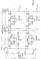
- each point (or element) image Pix i, j of the electroluminescent screen organic comprises two COM and COM 'control circuits of identical structure, associated with the organic light emitting diode OLED of this point Pix i, j .
- the OLED diode comprises a first electrode E1 by which it is current-controlled, and a second electrode E2 (cathode) connected to a potential VK common to all the diodes of the screen.
- this potential is the electric mass and is represented by a corresponding symbol.
- the two control circuits COM and COM ' are each connected at the output to the electrode E1 of the OLED diode. They have an identical structure. They each comprise a switching transistor, a current control transistor and a holding capacitance.
- T1, C1 and T2 these elements of the first circuit referenced COM and T1 ', C1' and T2 'these elements of the second circuit referenced COM'.
- These functions are: 1.-display video information, by applying a video voltage on the gate of the control transistor, to supply a current corresponding to the OLED diode and 2.-compensate the stress caused by the first function, by recovery phases during which a blocking voltage is applied to the gate of the control transistor.
- one of the two circuits for example the COM circuit, has the function of displaying the video information via the OLED diode, by applying a corresponding video voltage to the gate of its transistor. T2 whereas the other circuit, in the example COM ', has the function of applying a blocking voltage on the gate of its transistor T2', which puts this transistor in phase of recovery of the voltage drift of threshold, according to the invention.
- the functions of the two circuits are periodically reversed: the circuit COM 'then has the function of displaying the video information, by applying a corresponding video voltage on its transistor T2', while the circuit COM has the function of compensating the stress suffered by its transistor T2, by applying a blocking voltage.
- the period of inversion of the functions of the control circuits is preferably the frame period: at each new video frame, the functions of the circuits are reversed. More generally, it is possible to provide a function inversion for every K frames, K any integer. It will be seen that a corresponding addressing mode of the COM and COM 'circuits can easily be implemented using commercially available line and column drivers.
- the blocking voltage of the recovery phase may be a predetermined fixed voltage. It is advantageously variable. For each image point, it is advantageously a function of the video voltage applied to this image point. Indeed, the applied video voltage varies from one image element to another of the screen. For a given pixel, the video voltage also varies in time, from one frame to another. The drift of the threshold voltages is thus variable from one pixel to another. For this reason, by fixing the blocking voltage, an image with non-uniform luminance is obtained, despite the recovery phase.
- the blocking voltage is such that it applies to the current control transistor a reverse amplitude stress of the video voltage, it implements an intelligent recovery of the drift of the threshold voltage.
- each picture element Pix i, j corresponds to a selection line S i to which are connected the gates of the switching transistors T1 and T1 ', a first data line D j and a second data line D j '.
- the first data line D j is connected to the switching transistor of one of the control circuits, and the second data line D j 'is connected to the switching transistor of the other control circuit.
- D j is connected to the switching transistor T1 of the circuit COM and D j 'is connected to the switching transistor T1' of the circuit COM '.
- the data line D j will supply the video voltage Vv and the data line D j 'will supply the blocking voltage Vb. It is the current control transistor T2 which will then supply the current to the OLED diode, while the transistor T2 'will be in the recovery phase.
- the line D j will provide the blocking voltage Vb and the data line D j 'will provide the video voltage Vv. It is then the current control transistor T2 'which will supply the current to the OLED diode, while the transistor T2 will be in the recovery phase.
- FIG. 5 An example of a corresponding addressing sequence is schematically illustrated on the figure 5 , which highlights the dual behavior of transistors T2 and T2 ': when one is in the display phase, the other is in the recovery phase and vice versa.
- the blocking voltage Vb applied to a pixel is a predetermined fixed voltage, or advantageously a variable voltage from one pixel to another, which is a function of the video voltage applied to the pixel.
- a column driver usually used in LCD liquid crystal displays.
- these drivers are designed to provide a so-called mirror voltage, a function of the applied video voltage. More specifically, they usually output, for a given row of pixels, the video voltage to be applied to each data line D j of the matrix, a function of the video signal DATA VIDEO received at the input, or a corresponding mirror voltage.
- the image point of an LCD screen is a liquid crystal cell with a pixel electrode, to which the video voltage is applied, and a counter electrode common to all the pixels, brought to a reference voltage.
- the mirror voltage of a given video voltage is such that the direction of the electric field across the pixel is reversed, but provides the same luminance (the same gray level).
- the column drivers of the LCDs thus usually provide the output, for each data line of the matrix, one or the other voltage, depending on the frame, frame inversion, and / or depending on the pixel column concerned, inversion column.
- column inversion we will thus have the following operation: on a frame, the video voltage is applied to the data lines D j , D j + 2 , D j + 4 ; and the mirror voltage on the data lines D j + 1 , D j + 3 , D j + 5 .
- the mirror voltage is applied to the data lines D j , D j + 2 , D j + 4 ; and the video voltage is applied to the data lines D + 1 , D + 3 , D + 5 and so on.
- the mirror voltage is defined with respect to the counter-electrode voltage to obtain the same transmission coefficient on the pixel as with the video voltage. We generally speak of positive voltage for the video voltage and negative voltage for the mirror voltage.
- the mirror voltage has an inverse amplitude corresponding to the video voltage: this definition applies very well to the notion of variable blocking voltage, a function of the video voltage: it is a question of applying a stress in tension, of inverse amplitude, negative with respect to the voltage stress caused by the video voltage which controls the current conduction.
- the value of this inverse amplitude is in practice determined by measurement, so as to optimally compensate the stress brought by the video voltage.
- the blocking voltage to be applied to compensate a video voltage of a given amplitude can be determined by appropriate measurements. It is thus possible to define a correspondence table applicable to a given screen. It then suffices to use appropriate resistor values in the voltage divider circuit which usually provides the corresponding video voltage and mirror voltage levels.
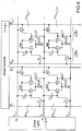
- the figure 6 illustrates another embodiment of the invention.
- the control of the two control circuits COM and COM ' uses both two selection lines of the screen S i and S i-1 , and two data lines D j and D j '.
- This embodiment corresponds to an addressing mode of the so-called inverted vertical scanning matrix: during a frame, the selection lines are sequentially addressed in the up-down direction, and at the following frame they are addressed sequentially addressed in the sense low to high.
- each pixel Pix i, j is mapped to the selection line Si to which is connected the gate of the switching transistor of one of the control circuits and another selection line of the matrix, preferably the previous selection line S i-1 , to which is connected the gate of the switching transistor of the other control circuit.
- a first data line D j and a second data line D j ' are furthermore matched.
- the first data line D j is connected to the switching transistor of one of the control circuits, and the second data line D j 'is connected to the switching transistor of the other control circuit.
- the gate of the switching transistor T1 of the circuit COM is connected to S i
- the gate of the switching transistor T1 'of the circuit COM' is connected to S i-1
- D i is connected to the switching transistor T1 of the COM circuit
- D i is connected to the switching transistor T1 'of the circuit COM'.
- the holding capacity of one of the control circuits is connected to the selection line which controls the gate of switching transistor of the other control circuit.
- the holding capacitance C1 of the control circuit COM is connected to the selection line S i-1 which is connected to the gate of the transistor T1 'of the control circuit COM.
- the holding capacitance C1 'of the control circuit COM' is connected to the selection line S i which is connected to the gate of the transistor T1 of the control circuit COM.
- Vdd reference voltage
- a corresponding addressing sequence is illustrated on the figure 8a . It highlights that the respective periods of display phase and recovery are not equal for the two transistors T2 and T2 'of a pixel, because of the alternation of vertical scanning. In the illustrated example, the recovery phase of transistor T2 is longer than its display phase. For the transistor T2 ', it is the opposite. In practice, the duration of the display and recovery phases of the transistors T2 and T2 'of a pixel Pix i, j depend on the rank i of the corresponding selection line S i . In practice, a rest period is provided between the end of the scanning of the lines of a frame and the beginning of the scanning of the lines of the following frame.
- the blocking voltage can be fixed or depending on the video voltage.
- a column driver of the state of the art of the LCD screens to address the data lines of a screen according to the figure 6 .
- the driver will then be used to control the data lines D j , D j 'as described in the previous embodiment, with in addition the inversion of the presentation of the video data in the scanning direction of the selection lines S i .
- the column driver applies the video voltage to the data lines D j ; and the mirror, blocking voltage on the data lines D j ', and in the successive order of the lines S i scanned from top to bottom.
- the column driver applies the mirror, blocking voltage on the data lines D j 'and the video voltage on the data lines D j , and in the successive order of the data. lines S i scanned from bottom to top, and so on from frame to frame.
- control circuits COM and COM ' are identical to the circuit of the state of the art ( Figure 1 ).
- the alternating control of their current control transistors T2 and T2 ' being obtained by the selection and data lines which drive their switching transistors T1 and T1', doubling the number of data lines to be driven.
- the gate of the switching transistor of one control circuit is connected to the selection line of the pixel Pix i, j , and the gate of the switching transistor of the other control circuit is connected to a another selection line that we note S i '.
- the addressing of the matrix can be likened to a line inversion type addressing for the LCD with the selection lines S i which address the video and the lines S i 'which address the recovery and vice versa to the next frame.
- the video / recovery alternation for the control circuits of a given pixel is done on the same column: we have a time to display the video voltage and a time to send the recovery voltage .
- the blocking voltage may be the video reverse voltage of the video that has been applied to the previous frame (column driver output) or a predetermined reset voltage. This reset voltage can then for example be applied to the columns by multiplexing, using a built-in column driver diagram with 3 TFT transistors, such as that described in the application. EP0815552 : either the driver output is sent on the columns or the reset voltage.
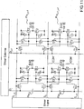
- FIG 11 Another embodiment of the invention is illustrated on the figure 11 .
- This embodiment has the advantage over the two embodiments described above to use the only lines of selection and usual data of the screen.
- each pixel Pix i, j is mapped to a single data line D j which is connected to switching transistors T1 and T1 'of the two control circuits.
- COM and COM ' a first selection line S i to which is connected the gate of the switching transistor of one of the control circuits and another selection line of the matrix, preferably the preceding line S i-1 , to which is connected the gate of the switching transistor of the other control circuit.
- S i is connected to the gate of the switching transistor T1 of the COM circuit
- S i-1 is connected to the gate of the switching transistor T1 'of the circuit COM'.
- the elements T1, C1 and T2 of the COM circuit and T1 ', C1' and T2 'of the circuit COM' are connected to each other and to the diode as before ( figures 1 , 3 , 6 ).
- the additional switching transistor provided in each control circuit is connected between the gate of the current control transistor and the gate of the switching transistor.
- the gate of this additional transistor is connected to the selection line associated with the other control circuit.
- the control circuit COM comprises an additional transistor T3 connected between the gate of the switching transistor T1 and the gate of the current control transistor T2. This additional transistor has its gate connected to the selection line S i-1 .
- the holding capacity in each control circuit is connected to the reference voltage V DD .
- V DD the reference voltage
- each control circuit make it possible to obtain alternating blocking of the current control transistors by switching the voltage level Vgoff of the unaddressed selection lines. Indeed, each selection line is forced to a Vgoff level, as long as it is not addressed. This Vgoff level is such that the switching transistor is off. When addressed, it is carried for a line time at a voltage level Vgon, so that the switching transistors connected to that line go to the "on" state and switch the voltage present on the data line, on the gate of the current control transistor.
- the transistors T1, T2, T3, T1 ', T2', T3 ' are all of the same type, N in the example, to be switched to the on state by a Vgon level on their gate and in the off state by a Vgoff level on their grid.
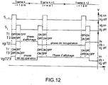
- FIG. 12 An example of a corresponding addressing sequence is schematically illustrated on the figure 12 , which highlights the dual behavior of transistors T2 and T2 '.
- This embodiment uses an inverted vertical scanning addressing mode to provide dual control of the two current control circuits alternately.
- the Vgoff level is used as the blocking voltage of the current control transistors, which is appropriately switched by the additional transistors T3.
- the gate and the drain of the additional transistors T3 and T3 ' can be connected to the selection lines in different arrangements. What matters is getting the Vgoff switching command at the right time.
- the pixels of the selection line S i it is possible, for example, to connect the gate of the transistors T3 to the previous selection line S i-1 and its drain to the current selection line S i , and the gate of the transistors T3. at the previous selection line S i + 1 and their drain at the selection line S i .
- the durations of the display and recovery phases are not equal for the two transistors T2 and T2 '. These durations can be converged by applying the same principles explained on page 13, lines 19 and following.
- the column drivers usually used in the liquid crystal displays LCD which advantageously thus provide a variable blocking voltage, which is a function of the video voltage, and whose different addressing modes (line, column, point, field ) allow to control the diode with a cycle ratio of 100%, while ensuring the alternation of the display and recovery phases on the current control transistors.
- the invention that has just been described is particularly applicable to organic electroluminescent screens, which use an active matrix with TFT (amorphous silicon) transistors. It applies more generally to organic electroluminescent displays with active matrix.
- TFT amorphous silicon
Description
La présente invention concerne un écran électroluminescent organique, et plus particulièrement un écran électroluminescent organique de type à matrice active, ou AMOLED (Active Matrix Organic Light Emitting Diode). The present invention relates to an organic electroluminescent screen, and more particularly to an organic electroluminescent screen of active matrix type, or AMOLED ( Active Matrix Organic Light Emitting Diode).
Dans un écran électroluminescent organique, l'élément image (pixel) est une structure à diode électroluminescente organique. Un tel écran ne nécessite pas de source de lumière additionnelle, contrairement à d'autres dispositifs d'affichage tels que les dispositifs dits LCD (Liquid Crystal Display). Il a comme autres avantages, de consommer peu, d'avoir une grande brillance, et des coûts de fabrication réduits. Le principe à la base de l'affichage de données vidéo par des diodes OLED est la modulation du courant de la diode. Ceci est obtenu par un transistor de commande en courant, qui reçoit sur sa grille une tension correspondant à la donnée vidéo à afficher et fournit un courant correspondant à la diode.In an organic electroluminescent screen, the image element (pixel) is an organic light-emitting diode structure. Such a screen does not require an additional light source, unlike other display devices such as devices called LCD ( Liquid Crystal Display). It has other advantages, to consume little, to have a great brilliance, and reduced manufacturing costs. The basic principle behind the display of video data by OLED diodes is the modulation of the current of the diode. This is obtained by a current control transistor, which receives on its gate a voltage corresponding to the video data to be displayed and supplies a current corresponding to the diode.
Sur la
De manière habituelle, à chaque nouvelle trame vidéo, les rangées de pixels sont sélectionnées en séquence par l'application sur leur ligne de sélection respective S1, S2, ...Sm, d'une tension de sélection Vgon, pendant un temps ligne. Les signaux de données vidéo correspondant à une rangée de pixels sélectionnée sont appliqués sur les lignes de données D1, ...Dj. Ces lignes de sélection et de données sont pilotées par des circuits de commande respectifs, appelés driver ligne et driver colonne, qui peuvent être intégrés à la matrice ou externes. Ces circuits sont bien connus de l'homme de l'art.In the usual way, at each new video frame, the rows of pixels are selected in sequence by the application on their respective selection line S 1 , S 2 , ... S m , of a selection voltage Vgon, during a time line. The video data signals corresponding to a selected pixel row are applied to the data lines D 1 , ... D j . These selection lines and data are controlled by respective control circuits, called line driver and column driver, which can be integrated into the matrix or external. These circuits are well known to those skilled in the art.
Considérons l'élément image Pixi,j. Lorsque la ligne de sélection Si est adressée, le transistor de commutation T1 devient passant, "on" pendant le temps d'adressage (temps ligne) de la ligne. Il commute la tension vidéo présente sur la ligne de donnée Dj, sur la grille du transistor T2 de commande en courant. Le transistor T1 repasse ensuite à l'état off et isole le pixel de la ligne de donnée. La capacité C1 assure alors le maintien de la tension sur la grille du transistor T2. Le transistor T2 fonctionne comme une source de courant commandée : il fournit à la diode OLED un courant dont l'intensité est fonction de la tension vidéo commutée sur sa grille. La diode OLED émet avec une intensité lumineuse correspondante. Dans ce fonctionnement, le transistor T2 est alimenté en continu : le rapport de cycle d'application de cette tension est donc de 100% pour chaque trame vidéo. La diode est aussi commandée en continu, avec un rapport de cycle de 100%.Consider the pixel element Pix i, j . When the selection line S i is addressed, the switching transistor T1 becomes on, "on" during the addressing time (line time) of the line. It switches the video voltage present on the data line D j , on the gate of the current control transistor T2. The transistor T1 then returns to the off state and isolates the pixel from the data line. The capacitor C1 then maintains the voltage on the gate of transistor T2. The transistor T2 operates as a controlled current source: it supplies the OLED diode with a current whose intensity is a function of the video voltage switched on its gate. The OLED emits with a corresponding light intensity. In this operation, the transistor T2 is fed continuously: the application cycle ratio of this voltage is therefore 100% for each video frame. The diode is also continuously controlled, with a cycle ratio of 100%.
L'intensité du courant passant dans le transistor de commande en courant T2 dépend du niveau de tension commuté sur la grille du transistor T2. Elle dépend aussi de la tension de seuil (threshold voltage) de ce transistor. On rappelle que la tension de seuil d'un transistor représente la différence de potentiel minimum qu'il faut appliquer entre grille et source du transistor pour que ce dernier passe du courant : en dessous le transistor est dit bloqué. Plus la différence de potentiel est élevée, plus le transistor passe du courant, jusqu'à être dans l'état saturé. Le courant drain-source Ids est donné par l'équation générale suivante : Ids=K(Vgs-Vth)2, où Vth est la tension de seuil, et Vgs la tension grille-source.The intensity of the current flowing in the current control transistor T2 depends on the voltage level switched on the gate of the transistor T2. It also depends on the threshold voltage of this transistor. It is recalled that the threshold voltage of a transistor represents the minimum potential difference that must be applied between the gate and the source of the transistor so that the latter passes current: below the transistor is said to be blocked. The higher the potential difference, the more the transistor goes from the current until it is in the saturated state. The current drain-source Ids is given by the following general equation: Ids = K (V gs -V th ) 2 , where V th is the threshold voltage, and V gs the gate-source voltage.
Pour avoir une bonne luminance et une bonne uniformité de l'écran, le courant Ids correspondant à un niveau de gris donné doit être constant dans le temps quel que soit le pixel de l'écran considéré.To have a good luminance and a good uniformity of the screen, the current Ids corresponding to a given gray level must be constant in time regardless of the pixel of the screen considered.
Dans l'invention, on s'intéresse plus particulièrement à des écrans AMOLED, dont les transistors de la matrice active (les transistors T1 et T2 des pixels Pixi,j) sont des transistors en couches minces dits TFT (Thin Film Transistor), et notamment à des écrans AMOLED utilisant une matrice active à transistors TFT à silicium amorphe, matrices qui sont avantageusement peu coûteuses. Dans ces écrans, on observe une forte dérive en positif de la tension de seuil du transistor T2 de commande en courant avec le niveau de la tension appliquée sur sa grille en continu (rapport de cycle de 100%). Plus généralement, la tension de seuil de ces transistors varie avec la température, la tension grille source qui lui est appliquée et le rapport de cycle, c'est à dire le temps pendant lequel la tension Vgs est appliquée rapportée à la durée de la trame. Ceci concerne aussi d'autres types de transistors, par exemple des transistors dans des matériaux entre le silicium amorphe et le silicium polycristallin.In the invention, one is more particularly interested in AMOLED screens, whose transistors of the active matrix (the transistors T1 and T2 of the pixels Pix i, j ) are thin film transistors known as TFT ( Thin Film Transistor ) , and in particular to AMOLED screens using an active matrix with amorphous silicon TFT transistors, which matrices are advantageously inexpensive. In these screens, there is a strong positive drift of the threshold voltage of the current control transistor T2 with the level of the voltage applied to its gate continuously (100% cycle ratio). More generally, the threshold voltage of these transistors varies with the temperature, the source gate voltage applied to it and the cycle ratio, ie the time during which the voltage Vgs is applied relative to the duration of the frame. . This also relates to other types of transistors, for example transistors in materials between amorphous silicon and polycrystalline silicon.
Sur la
Pour une donnée à afficher donnée, le niveau de lumière obtenu est donc variable suivant la tension de seuil effective du transistor, au moment de l'observation. La tension de seuil dérivant en positif, le courant fourni par les transistors de commande en courant diminue, ce qui se traduit par une perte de luminance sur les écrans AMOLED.For a given data to be displayed, the level of light obtained is therefore variable according to the effective threshold voltage of the transistor, moment of observation. Since the threshold voltage is positive, the current supplied by the current control transistors decreases, which results in a loss of luminance on the AMOLED screens.
Les tensions vidéo à afficher étant variables d'un pixel à l'autre, cette variation de la tension de seuil des transistors de commande T2 se traduit en outre par une forte non-uniformité sur l'écran AMOLED.The video voltages to be displayed being variable from one pixel to another, this variation of the threshold voltage of the control transistors T2 also results in a strong non-uniformity on the AMOLED screen.
Un objet de l'invention est de résoudre ce problème de dégradation de l'affichage des écrans AMOLEDs dû à la dérive de la tension de seuil des transistors de commande en courant qui pilotent les diodes électroluminescentes organiques.An object of the invention is to solve this problem of degradation of the display of AMOLEDs screens due to the drift of the threshold voltage of the current control transistors which drive the organic light emitting diodes.
Une solution à ce problème technique a été trouvée dans l'invention qui consiste principalement à prévoir une phase de récupération de la dérive de la tension de seuil du transistor de commande en courant de chaque pixel. Pendant cette phase de récupération, on bloque le transistor de commande en courant, par une valeur de tension de blocage appliquée sur sa grille. Le transistor subit alors un stress inverse de celui subit pendant la période d'affichage, en sorte que la tension de seuil revienne autour de sa valeur initiale Vth0. Comme, la diode doit être commandée avec un rapport de cycle de 100%, on prévoit ainsi un premier et un deuxième transistors de commande en courant par diode, commandés de façon appropriée, en sorte que pendant que l'un commande le courant dans la diode, l'autre est bloqué et vice et versa. En moyenne, sur chaque transistor, la dérive de la tension de seuil est nulle.One solution to this technical problem has been found in the invention which consists mainly in providing a phase for recovering the drift of the threshold voltage of the current control transistor of each pixel. During this recovery phase, the current control transistor is blocked by a blocking voltage value applied to its gate. The transistor is then subjected to a reverse stress from that experienced during the display period, so that the threshold voltage returns around its initial value Vth 0 . Since the diode must be controlled with a cycle ratio of 100%, a first and a second diode current control transistors, appropriately controlled, are provided so that while one drives the current in the diode, the other is blocked and vice versa. On average, on each transistor, the drift of the threshold voltage is zero.
La publication
Dans un contexte d'écran LCD dit séquentiel couleur, la demande de brevet
Un objet de l'invention est de proposer écran AMOLED offrant de meilleures performances à coût minimal en termes de circuits et de commande d'adressage.An object of the invention is to provide an AMOLED display that provides better performance at minimum cost in terms of circuits and addressing control.
L'invention concerne donc un écran électroluminescent organique comprenant n.m point images organisés matriciellement suivant m rangées et n colonnes, chaque point image comprenant une diode organique (OLED) et un premier et un deuxième circuits de commande en courant (COM,COM') de ladite diode qui comprennent chacun :
- un transistor de commande en courant (T2) connecté entre une tension de référence et une électrode (E1) de ladite diode,
- un transistor de commutation (T1) pour commuter une tension de grille sur la grille dudit transistor de commande en courant,
- une capacité (C1) connectée sur la grille dudit transistor de commande en courant, pour maintenir ladite tension de grille,
caractérisé en ce que
le circuit d'adressage comprend m lignes de sélection de rangée, une par rangée de la matrice et les points images d'une rangée de la matrice sont connectés à une ligne de sélection respective (Si) de ladite rangée et à une autre ligne de sélection d'une autre rangée, et n lignes de données, une par colonne de la matrice, chacune pour appliquer une tension vidéo à un point image d'une colonne respective et d'une rangée courante sélectionnée, et le circuit d'adressage est configuré pour sélectionner en séquence chacune des lignes de sélection de l'écran, dans le sens d'un balayage de l'écran de haut en bas pour une trame, et dans le sens d'un balayage de l'écran de bas en haut pour la trame suivante,
et en ce que dans chaque point image sur une rangée et une colonne respectives de la matrice :
- la ligne de donnée respective (Di) est connectée aux transistors de commutation (T1, T1') des deux circuits de commande associés,
- la ligne de sélection (Si) respective est connectée à la grille du transistor de commutation (T1) d'un des deux circuits de commande (COM),
- l'autre ligne de sélection (Si-1) est connectée à la grille du transistor de commutation (T1') de l'autre circuit de commande (COM'), et
- chacun des deux circuits de commande (COM, COM') comprend un transistor supplémentaire (T3, T3') pour appliquer une tension de blocage comme tension de grille du transistor de commande du circuit de commande considéré, ledit transistor étant connecté entre la grille du transistor de commande en courant du circuit de commande considéré et la ligne de sélection qui lui est associée, et commandé sur sa grille par l'autre ligne de sélection associée à l'autre circuit de commande.
- a current control transistor (T2) connected between a reference voltage and an electrode (E1) of said diode,
- a switching transistor (T1) for switching a gate voltage on the gate of said current control transistor,
- a capacitance (C1) connected to the gate of said current control transistor, for maintaining said gate voltage,
characterized in that
the addressing circuit comprises m row selection lines, one per row of the matrix and the image points of one row of the array are connected to a respective selection line (Si) of said row and to another row of selecting another row, and n rows of data, one per column of the array, each for applying a video voltage to an image point of a respective column and a current selected row, and the addressing circuit is configured to sequentially select each of the screen selection lines, in the direction of a screen scan from top to bottom for a frame, and in the direction of a bottom-up scan of the screen for the next frame,
and in that each image point on a respective row and column of the matrix:
- the respective data line (D i ) is connected to the switching transistors (T1, T1 ') of the two associated control circuits,
- the respective selection line (S i ) is connected to the gate of the switching transistor (T1) of one of the two control circuits (COM),
- the other selection line (S i-1 ) is connected to the gate of the switching transistor (T1 ') of the other control circuit (COM'), and
- each of the two control circuits (COM, COM ') comprises an additional transistor (T3, T3') for applying a blocking voltage as the gate voltage of the control transistor of the control circuit under consideration, said transistor being connected between the gate of the current control transistor of the control circuit considered and the selection line associated with it, and controlled on its gate by the other selection line associated with the other control circuit.
Avantageusement, il est fait usage des drivers de commande lignes qui pilotent les lignes de sélection et/ou des drivers colonnes qui pilotent les lignes de données dans les écrans à cristaux liquides (LCD) pour piloter ces circuits de façon appropriée.Advantageously, use is made of the line control drivers that control the selection lines and / or column drivers that drive the data lines in the liquid crystal displays (LCD) to drive these circuits appropriately.
D'autres avantages et caractéristiques de l'invention sont détaillés dans la description suivante en référence aux dessins illustrés de modes de réalisation de l'invention, donnés à titre d'exemple non limitatif. Dans ces dessins :
- la
figure 1 déjà décrite illustre la structure d'un élément image à diode OLED selon l'état de l'art; - la
figure 2 illustre le phénomène connu de dérive de la tension de seuil d'un transistor ; - la
figure 3 illustre une structure d'élément image à diode OLED pour un circuit d'adressage de n.m points images utilisant m lignes de sélection et 2. n lignes de données pour commander en alternance des phases de récupération et d'adressage des transistors de commande des points OLED; - les
figures 4 et 5 illustrent un mode et une séquence d'adressage correspondants; - la
figure 6 illustre une variante à m lignes de sélection et 2.n lignes de données; et - les
figures 7, 8a et8b illustrent un mode et des séquences d'adressage correspondants; - la
figure 9 illustre une structure d'élément image à diode OLED pour un circuit d'adressage de n.m points images utilisant 2.m lignes de sélection et n lignes de données pour la commande alternée des phases de récupération et d'adressage; - la
figure 10 illustre un mode d'adressage correspondant ; - la
figure 11 illustre une structure d'élément image à diode OLED pour un circuit d'adressage de n.m points images utilisant m lignes de sélection et n lignes de données pour la commande alternée des phases de récupération et d'adressage; et - la
figure 12 illustrent une séquence d'adressage correspondante.
- the
figure 1 already described illustrates the structure of an OLED diode image element according to the state of the art; - the
figure 2 illustrates the known phenomenon of drift of the threshold voltage of a transistor; - the
figure 3 illustrates an OLED diode picture element structure for an n-point addressing circuit using m selection lines and 2. n data lines for alternately controlling recovery and addressing phases of the dot control transistors OLED; - the
Figures 4 and 5 illustrate a corresponding mode and sequence of addressing; - the
figure 6 illustrates a variant with m rows of selection and 2.n lines of data; and - the
Figures 7, 8a and8b illustrate a mode and corresponding addressing sequences; - the
figure 9 illustrates an OLED diode picture element structure for an nm point pixel addressing circuit using 2.m selection lines and n data lines for alternating control of the recovery and addressing phases; - the
figure 10 illustrates a corresponding addressing mode; - the
figure 11 illustrates an OLED diode picture element structure for an n-point addressing circuit using m selection lines and n data lines for alternating control of the recovery and addressing phases; and - the
figure 12 illustrate a corresponding addressing sequence.
Dans un souci de clarté et de simplification de l'exposé, les éléments communs aux différentes figures portent les même références. Sur les figures, on note Vg(T2) et Vg(T2'), les tensions appliquées sur les grilles des transistors T2 et T2'.For the sake of clarity and simplification of the presentation, the elements common to the different figures bear the same references. In the figures, Vg (T2) and Vg (T2 ') are noted, the voltages applied to the gates of the transistors T2 and T2'.
Selon l'invention et comme illustré sur les
Les deux circuits de commande COM et COM' sont chacun connectés en sortie à l'électrode E1 de la diode OLED. Ils ont une structure identique. Ils comprennent chacun un transistor de commutation, un transistor de commande en courant et une capacité de maintien. Par convention, on note T1, C1 et T2 ces éléments du premier circuit référencé COM et T1', C1' et T2' ces éléments du deuxième circuit référencé COM'.The two control circuits COM and COM 'are each connected at the output to the electrode E1 of the OLED diode. They have an identical structure. They each comprise a switching transistor, a current control transistor and a holding capacitance. By convention, we denote T1, C1 and T2 these elements of the first circuit referenced COM and T1 ', C1' and T2 'these elements of the second circuit referenced COM'.
Selon l'invention, ces circuits COM et COM' sont commandés par des lignes de sélection et/ou de données de la matrice de telle sorte qu'ils aient une fonction différente à chaque trame vidéo, ces fonctions étant inversées périodiquement. Ces fonctions sont : 1.-afficher une information vidéo, par application d'une tension vidéo sur la grille du transistor de commande, pour fournir un courant correspondant à la diode OLED et 2.-compenser le stress occasionné par la première fonction, par des phases de récupération pendant lesquelles une tension de blocage est appliquée sur la grille du transistor de commande.According to the invention, these circuits COM and COM 'are controlled by selection lines and / or data of the matrix so that they have a different function for each video frame, these functions being periodically reversed. These functions are: 1.-display video information, by applying a video voltage on the gate of the control transistor, to supply a current corresponding to the OLED diode and 2.-compensate the stress caused by the first function, by recovery phases during which a blocking voltage is applied to the gate of the control transistor.
Ainsi, pendant une trame vidéo donnée, l'un des deux circuits, par exemple le circuit COM, a la fonction d'afficher l'information vidéo via la diode OLED, par application d'une tension vidéo correspondante sur la grille de son transistor T2, alors que l'autre circuit, dans l'exemple COM', a la fonction d'appliquer une tension de blocage sur la grille de son transistor T2', ce qui met ce transistor en phase de récupération de la dérive de tension de seuil, selon l'invention. Les fonctions des deux circuits sont inversées périodiquement : le circuit COM' a alors la fonction d'afficher l'information vidéo, par application d'une tension vidéo correspondante sur son transistor T2', tandis que le circuit COM a la fonction de compenser le stress subit par son transistor T2, en lui appliquant une tension de blocage.Thus, during a given video frame, one of the two circuits, for example the COM circuit, has the function of displaying the video information via the OLED diode, by applying a corresponding video voltage to the gate of its transistor. T2, whereas the other circuit, in the example COM ', has the function of applying a blocking voltage on the gate of its transistor T2', which puts this transistor in phase of recovery of the voltage drift of threshold, according to the invention. The functions of the two circuits are periodically reversed: the circuit COM 'then has the function of displaying the video information, by applying a corresponding video voltage on its transistor T2', while the circuit COM has the function of compensating the stress suffered by its transistor T2, by applying a blocking voltage.
Une trame sur deux en moyenne étant mise à profit pour chaque circuit de commande pour destresser son transistor de commande en courant, la dérive moyenne de la tension de seuil de chaque transistor de commande de la matrice active est nulle ou approximativement nulle. Ceci peut être obtenu sans affecter le rapport de cycle d'application de la tension vidéo sur la diode OLED, en sorte que la diode reste commandée en continue (rapport de cycle de 100%).An average of every second frame is used for each control circuit to de-stress its control transistor. current, the average drift of the threshold voltage of each control transistor of the active matrix is zero or approximately zero. This can be achieved without affecting the duty cycle ratio of the video voltage on the OLED diode, so that the diode remains continuously controlled (100% duty cycle).
La période d'inversion des fonctions des circuits de commande est de préférence, la période trame : à chaque nouvelle trame vidéo, les fonctions des circuits sont inversés. Plus généralement, on peut prévoir une inversion des fonctions tous les K trames, K nombre entier quelconque. On verra qu'un mode d'adressage correspondant des circuits COM et COM' peut être facilement mise en oeuvre en utilisant des drivers ligne et colonne du commerce.The period of inversion of the functions of the control circuits is preferably the frame period: at each new video frame, the functions of the circuits are reversed. More generally, it is possible to provide a function inversion for every K frames, K any integer. It will be seen that a corresponding addressing mode of the COM and COM 'circuits can easily be implemented using commercially available line and column drivers.
La tension de blocage de la phase de récupération peut-être une tension fixe prédéterminée. Elle est avantageusement variable. Pour chaque point image, elle est avantageusement fonction de la tension vidéo appliquée sur ce point image. En effet, la tension vidéo appliquée varie d'un élément image à l'autre de l'écran. Pour un pixel donné, la tension vidéo varie aussi dans le temps, d'une trame à une autre. La dérive des tensions de seuil est ainsi variable d'un pixel à l'autre. Pour cette raison, en fixant la tension de blocage, on obtient une image avec une luminance non uniforme, malgré la phase de récupération. En prévoyant avantageusement que la tension de blocage soit telle qu'elle applique au transistor de commande en courant un stress d'amplitude inverse de la tension vidéo, on met en oeuvre une récupération intelligente de la dérive de la tension de seuil.The blocking voltage of the recovery phase may be a predetermined fixed voltage. It is advantageously variable. For each image point, it is advantageously a function of the video voltage applied to this image point. Indeed, the applied video voltage varies from one image element to another of the screen. For a given pixel, the video voltage also varies in time, from one frame to another. The drift of the threshold voltages is thus variable from one pixel to another. For this reason, by fixing the blocking voltage, an image with non-uniform luminance is obtained, despite the recovery phase. Advantageously providing that the blocking voltage is such that it applies to the current control transistor a reverse amplitude stress of the video voltage, it implements an intelligent recovery of the drift of the threshold voltage.
Considérons le mode de réalisation selon l'invention illustré à la
Plus précisément, à chaque élément image Pixi,j correspond une ligne de sélection Si à laquelle sont connectées les grilles des transistors de commutation T1 et T1', une première ligne de donnée Dj et une deuxième ligne de données Dj'. La première ligne de donnée Dj est connectée au transistor de commutation de l'un des circuits de commande, et la deuxième ligne de donnée Dj' est connectée au transistor de commutation de l'autre circuit de commande. Ainsi dans l'exemple, Dj est connectée au transistor de commutation T1 du circuit COM et Dj' est connectée au transistor de commutation T1' du circuit COM'.More precisely, at each picture element Pix i, j corresponds to a selection line S i to which are connected the gates of the switching transistors T1 and T1 ', a first data line D j and a second data line D j '. The first data line D j is connected to the switching transistor of one of the control circuits, and the second data line D j 'is connected to the switching transistor of the other control circuit. Thus, in the example, D j is connected to the switching transistor T1 of the circuit COM and D j 'is connected to the switching transistor T1' of the circuit COM '.
Comme illustré sur la
Pendant une autre trame vidéo, par exemple la trame suivante k+1, ce sera l'inverse : la ligne Dj va fournir la tension de blocage Vb et la ligne de donnée Dj' va fournir la tension vidéo Vv. C'est alors le transistor de commande en courant T2' qui fournira le courant à la diode OLED, tandis que le transistor T2 sera en phase de récupération.During another video frame, for example the following frame k + 1, it will be the opposite: the line D j will provide the blocking voltage Vb and the data line D j 'will provide the video voltage Vv. It is then the current control transistor T2 'which will supply the current to the OLED diode, while the transistor T2 will be in the recovery phase.
Un exemple de séquence d'adressage correspondant est illustré schématiquement sur la
On a vu que la tension de blocage Vb appliquée sur un pixel est une tension fixe prédéterminée, ou avantageusement une tension variable d'un pixel à l'autre, fonction de la tension vidéo appliquée sur le pixel.It has been seen that the blocking voltage Vb applied to a pixel is a predetermined fixed voltage, or advantageously a variable voltage from one pixel to another, which is a function of the video voltage applied to the pixel.
On peut utiliser avantageusement comme driver colonne, pour piloter les 2n lignes de données d'un écran suivant le mode de réalisation de la
La tension miroir est définie par rapport à la tension de contre-électrode pour obtenir le même coefficient de transmission sur le pixel qu'avec la tension vidéo. On parle généralement de tension positive pour la tension vidéo et de tension négative pour la tension miroir.The mirror voltage is defined with respect to the counter-electrode voltage to obtain the same transmission coefficient on the pixel as with the video voltage. We generally speak of positive voltage for the video voltage and negative voltage for the mirror voltage.
Ainsi la tension miroir a une amplitude inverse correspondante à la tension vidéo : cette définition s'applique très bien à la notion de tension de blocage variable, fonction de la tension vidéo : il s'agit d'appliquer un stress en tension, d'amplitude inverse, négative par rapport au stress en tension provoqué par la tension vidéo qui commande la conduction en courant. La valeur de cette amplitude inverse est en pratique déterminée par mesure, de manière à compenser de façon optimale le stress apporté par la tension vidéo.Thus the mirror voltage has an inverse amplitude corresponding to the video voltage: this definition applies very well to the notion of variable blocking voltage, a function of the video voltage: it is a question of applying a stress in tension, of inverse amplitude, negative with respect to the voltage stress caused by the video voltage which controls the current conduction. The value of this inverse amplitude is in practice determined by measurement, so as to optimally compensate the stress brought by the video voltage.
La tension de blocage à appliquer pour compenser une tension vidéo d'amplitude donnée peut être déterminée par des mesures appropriés. On peut ainsi définir une table de correspondance applicable à un écran donné. Il suffit alors d'utiliser des valeurs de résistances appropriées dans le circuit diviseur de tension qui fournit habituellement les niveaux de tension vidéo et de tension miroir correspondantes.The blocking voltage to be applied to compensate a video voltage of a given amplitude can be determined by appropriate measurements. It is thus possible to define a correspondence table applicable to a given screen. It then suffices to use appropriate resistor values in the voltage divider circuit which usually provides the corresponding video voltage and mirror voltage levels.
On peut ainsi utiliser un tel driver colonne d'écran LCD pour commander les lignes de données d'un écran tel qu'illustré en
La
Ce mode de réalisation correspond un mode d'adressage de la matrice dit à balayage vertical inversé : pendant une trame, les lignes de sélection sont séquentiellement adressées dans le sens haut vers bas, et à la trame suivante elles sont adressées séquentiellement adressées dans le sens bas vers haut.This embodiment corresponds to an addressing mode of the so-called inverted vertical scanning matrix: during a frame, the selection lines are sequentially addressed in the up-down direction, and at the following frame they are addressed sequentially addressed in the sense low to high.
De manière plus détaillée, dans ce mode de réalisation de l'invention on fait correspondre à chaque élément image Pixi,j, la ligne de sélection Si à laquelle est connectée la grille du transistor de commutation de l'un des circuits de commande et une autre ligne de sélection de la matrice, de préférence la ligne de sélection précédente Si-1, à laquelle est connectée la grille du transistor de commutation de l'autre circuit de commande. A chaque pixel Pixi,j, on fait en outre correspondre une première ligne de donnée Dj et une deuxième ligne de données Dj'. La première ligne de donnée Dj est connectée au transistor de commutation de l'un des circuits de commande, et la deuxième ligne de donnée Dj' est connectée au transistor de commutation de l'autre circuit de commande. Ainsi dans l'exemple, la grille du transistor de commutation T1 du circuit COM est connectée à Si, la grille du transistor de commutation T1' du circuit COM' est connectée à Si-1 ; Di est connectée au transistor de commutation T1 du circuit COM et Dj' est connectée au transistor de commutation T1' du circuit COM'.In more detail, in this embodiment of the invention, each pixel Pix i, j is mapped to the selection line Si to which is connected the gate of the switching transistor of one of the control circuits and another selection line of the matrix, preferably the previous selection line S i-1 , to which is connected the gate of the switching transistor of the other control circuit. At each pixel Pix i, j , a first data line D j and a second data line D j 'are furthermore matched. The first data line D j is connected to the switching transistor of one of the control circuits, and the second data line D j 'is connected to the switching transistor of the other control circuit. Thus in the example, the gate of the switching transistor T1 of the circuit COM is connected to S i , the gate of the switching transistor T1 'of the circuit COM' is connected to S i-1 ; D i is connected to the switching transistor T1 of the COM circuit and D i is connected to the switching transistor T1 'of the circuit COM'.
Dans l'exemple, on a illustré une variante de connexion de la capacité de maintien des circuits de commande COM et COM' : la capacité de maintien de l'un des circuits de commande est connectée à la ligne de sélection qui commande la grille du transistor de commutation de l'autre circuit de commande. Ainsi la capacité de maintien C1 du circuit de commande COM est connectée à la ligne de sélection Si-1 qui est connectée à la grille du transistor T1' du circuit de commande COM.' La capacité de maintien C1' du circuit de commande COM' est connectée à la ligne de sélection Si qui est connectée à la grille du transistor T1 du circuit de commande COM. On pourrait comme précédemment avoir les capacités C1 et C1' connectées à la tension de référence Vdd.In the example, there is illustrated an alternative connection of the holding capacity of the COM and COM 'control circuits: the holding capacity of one of the control circuits is connected to the selection line which controls the gate of switching transistor of the other control circuit. Thus, the holding capacitance C1 of the control circuit COM is connected to the selection line S i-1 which is connected to the gate of the transistor T1 'of the control circuit COM. The holding capacitance C1 'of the control circuit COM' is connected to the selection line S i which is connected to the gate of the transistor T1 of the control circuit COM. As before, it would be possible to have the capacitors C1 and C1 'connected to the reference voltage Vdd.
Le mode de fonctionnement va alors être le suivant :
- Pendant une trame vidéo, la trame k par exemple, les lignes de sélection sont balayées en séquence du haut vers le bas, c'est à dire dans le sens des indices i croissants de 1 à m (
figure 1 ). Dans ce cas et comme illustré sur lafigure 7 , les lignes de données Dj sont pilotées pour transmettre les tensions vidéo et les lignes de données Dj' sont pilotées pour transmettre les tensions de blocage.
Lorsque la ligne de sélection Si-1 est adressée, par application pendant un temps ligne correspondant d'un niveau de tension Vgon, le transistor de commutation T1' du circuit COM' est passant. Il commute la tension de blocage présente à ce moment sur la colonne Dj' sur la grille du transistor T2' : le transistor T2' entre en phase de récupération.
Lorsque la ligne de sélection Si est adressée au temps ligne suivant, par application pendant le temps ligne correspondant, d'un niveau de tension Vgon, le transistor de commutation T1 du circuit COM est passant. Il commute la tension vidéo présente à ce moment sur la colonne Dj sur la grille du transistor T2 : le transistor T2 entre en phase d'affichage, et fournit le courant à la diode OLED. - Pendant la trame suivante k+1, les lignes de sélection sont balayées en séquence dans le sens inverse, c'est à dire du bas vers le haut ou encore dans le sens des indices i décroissants de m vers 1 (
figure 1 ) et le rôle des lignes de données Dj et Dj' est inversé : les lignes Dj transmettent les tensions de blocage et les lignes Dj' transmettent les tensions vidéo (figure 7 ). Lorsque la ligne de sélection Si est adressée, par application pendant un temps ligne correspondant d'un niveau de tension Vgon, le transistor de commutation T1 du circuit COM est passant. Il commute la tension de blocage présente sur la ligne de donnée Dj, sur la grille du transistor T2 et la capacité de maintien associée C1. Le transistor T2 est en phase de récupération. Lorsque la ligne de sélection Si-1 est ensuite adressée, par application pendant un temps ligne correspondant d'un niveau de tension Vgon, le transistor de commutation T1' du circuit COM' est passant. Il commute la tension vidéo présente sur la ligne de donnée Dj', sur la grille du transistor T2' et la capacité de maintien associée C1'. - Pendant cette trame k+1, c'est le transistor T2' qui est en phase d'affichage et le transistor T2 qui est en phase de récupération.
- During a video frame, the frame k for example, the selection lines are scanned in sequence from top to bottom, ie in the direction of increasing indices i from 1 to m (
figure 1 ). In this case and as illustrated on thefigure 7 , the data lines D j are driven to transmit the video voltages and the data lines D j 'are controlled to transmit the blocking voltages.
When the selection line S i-1 is addressed, by application during a corresponding line time of a voltage level Vgon, the switching transistor T1 'of the circuit COM' is conducting. It switches the blocking voltage present at this moment on the column D j 'on the gate of the transistor T2': the transistor T2 'enters the recovery phase.
When the selection line S i is addressed to the next line time, by application during the corresponding line time, of a voltage level Vgon, the switching transistor T1 of the COM circuit is on. It switches the video voltage present at this time on the column D j on the gate of the transistor T2: the transistor T2 enters the display phase, and supplies the current to the OLED diode. - During the following frame k + 1, the selection lines are scanned in sequence in the opposite direction, ie from the bottom upwards or in the direction of decreasing indices i from m to 1 (
figure 1 ) and the role of the data lines D j and D j 'is reversed: the lines D j transmit the blocking voltages and the lines D j' transmit the video voltages (figure 7 ). When the selection line S i is addressed, by application during a corresponding line time of a voltage level Vgon, the switching transistor T1 of the COM circuit is passing. It switches the blocking voltage present on the data line D j , on the gate of the transistor T2 and the associated holding capacity C1. The transistor T2 is in the recovery phase. When the selection line S i-1 is then addressed, by application during a corresponding line time of a voltage level Vgon, the switching transistor T1 'of the circuit COM' is conducting. It switches the video voltage present on the data line D j ', on the gate of the transistor T2' and the associated holding capacitor C1 '. - During this frame k + 1, it is the transistor T2 'which is in the display phase and the transistor T2 which is in the recovery phase.
Une séquence d'adressage correspondante est illustrée sur la
Pour converger vers des durées proches voire égales entre le balayage haut bas et bas haut on peut :
- adresser rapidement la matrice puis laisser un temps de repos avant le balayage suivant.
- balayer X fois toujours dans le même sens avant de commuter sur un balayage de X fois dans l'autre sens. Le tableau de la
figure 8b est une illustration qu'une telle alternance du balayage toutes les X =2 trames, on arrive à équilibrer les temps de récupération et vidéo entre COM et COM'. Sur cette figure, Vv(k) et Vb(k) représente les tensions vidéo et de blocage commutées sur les grilles des transistors T2 et T2' des pixels pour la ligne de sélection considérée appliquée pendant la trame k. Tant que la ligne de sélection considérée n'est pas sélectionnée, on a les niveaux de tension des grilles des transistors T2 et T2' sont ceux appliqués à la trame précédente k-1. Dans le tableau, on montre l'évolution des niveaux de tension pendant le temps trame, et pour quatre trames successives, pour une ligne du haut de l'écran, dans l'exemple S1, du milieu de l'écran (Sm/2), et du bas de l'écran (Sm).
- quickly address the matrix and leave a rest period before the next scan.
- scan X times in the same direction before switching X-scan in the other direction. The table of the
figure 8b is an illustration that such an alternation of scanning every X = 2 frames, we manage to balance the recovery time and video between COM and COM '. In this figure, Vv (k) and Vb (k) represents the switched video and blocking voltages on the gates of the transistors T2 and T2 'of the pixels for the selection line considered applied during the frame k. As long as the selection line under consideration is not selected, we have the voltage levels of the gates of transistors T2 and T2 'are those applied to the previous frame k-1. In the table, we show the evolution of the voltage levels during the frame time, and for four successive frames, for a line from the top of the screen, in the example S 1 , of the middle of the screen (S m / 2), and the bottom of the screen (S m).
La tension de blocage peut être fixe ou fonction de la tension vidéo. Dans ce dernier cas, et comme dans le mode de réalisation vu en relation avec la
On notera que le mode de réalisation de la
Dans les modes de réalisation de la
Dans une variante illustrée sur les
Comme illustré sur la
As illustrated on the
Un avantage de reporter sur le driver ligne la commande de l'alternance des fonctions d'affichage et de récupération des circuits de commande COM et COM' réside dans ce que les drivers lignes sont moins coûteux que les drivers colonnes en termes de complexité et de place. De plus, ces drivers peuvent être facilement intégrés sur le verre et notamment en technologie silicium amorphe.An advantage of reporting on the line driver the control of the alternation of the display and recovery functions of the COM and COM control circuits is that the line drivers are less expensive than the column drivers in terms of complexity and complexity. square. In addition, these drivers can be easily integrated on the glass and in particular in amorphous silicon technology.
Dans ce mode de réalisation, la grille du transistor de commutation d'un circuit de commande est connectée à la ligne de sélection du pixel Pixi,j, et la grille du transistor de commutation de l'autre circuit de commande est connectée à une autre ligne de sélection que l'on note Si'. Les lignes Si et Si' sont deux lignes successives du driver ligne Su et Su+1, avec u=1 à 2m, et i=1 à m.In this embodiment, the gate of the switching transistor of one control circuit is connected to the selection line of the pixel Pix i, j , and the gate of the switching transistor of the other control circuit is connected to a another selection line that we note S i '. The lines S i and S i 'are two successive lines of the line driver S u and S u + 1 , with u = 1 to 2m, and i = 1 to m.
L'adressage de la matrice peut s'apparenter à un adressage type inversion ligne pour le LCD avec les lignes de sélection Si qui adressent la vidéo et les lignes Si' qui adressent la récupération et inversement à la trame suivante.The addressing of the matrix can be likened to a line inversion type addressing for the LCD with the selection lines S i which address the video and the lines S i 'which address the recovery and vice versa to the next frame.
Un mode d'adressage de la matrice correspondant est illustré sur le tableau de la
Considérons le pixel Pixi,j.Consider the pixel Pix i, j .
Pendant une trame k, lorsque la ligne Su=Si est adressée, le transistor T1 est passant et commute la tension vidéo Vv présente à ce moment sur la ligne de donnée Dj, sur la grille du transistor T2 et la capacité C1.During a frame k, when the line S u = S i is addressed, the transistor T1 is on and switches the video voltage Vv present at that moment on the data line D j , on the gate of the transistor T2 and the capacitor C1.
Lorsque la ligne Su+1=Si' est adressée, le transistor T1' est passant et commute la tension vidéo Vb présente à ce moment sur la ligne de donnée Dj, sur la grille du transistor T2' et la capacité C1'.
Au niveau de la commande du driver colonne, l'alternance vidéo/récupération pour les circuits de commande d'un pixel donné est fait sur la même colonne : on a un temps pour afficher la tension vidéo et un temps pour envoyer la tension de récupération. Le nombre de lignes ayant doublé (u=2.m), le temps ligne est divisé par 2.
La tension de blocage peut être la tension vidéo inverse de la vidéo qui a été appliquée la trame précédente (sortie driver colonne) ou bien une tension de reset prédéterminée. Cette tension de reset peut alors par exemple être appliquée sur les colonnes par multiplexage, en utilisant un schéma de driver intégré colonne à 3 transistors TFT, tel que celui décrit dans la demande
At the level of the column driver command, the video / recovery alternation for the control circuits of a given pixel is done on the same column: we have a time to display the video voltage and a time to send the recovery voltage . The number of lines having doubled (u = 2.m), the line time is divided by 2.
The blocking voltage may be the video reverse voltage of the video that has been applied to the previous frame (column driver output) or a predetermined reset voltage. This reset voltage can then for example be applied to the columns by multiplexing, using a built-in column driver diagram with 3 TFT transistors, such as that described in the application.
Un autre mode de réalisation de l'invention est illustré sur la
Ceci est obtenu en prévoyant dans le circuit de commande un transistor de commutation supplémentaire, par lequel on va assurer la commande alternée des transistors de commande en courant. On note T3 pour le circuit COM et T3' pour le circuit COM' ce transistor supplémentaire du circuit de commande.Another embodiment of the invention is illustrated on the
This is achieved by providing in the control circuit an additional switching transistor, whereby the alternating control of the current control transistors will be ensured. Note T3 for the COM circuit and T3 'for the circuit COM' this additional transistor of the control circuit.
De manière plus détaillée, dans ce mode de réalisation de l'invention, on fait correspondre à chaque élément image Pixi,j, une seule ligne de donnée Dj qui est connectée aux transistors de commutation T1 et T1' des deux circuits de commande COM et COM', une première ligne de sélection Si à laquelle est connectée la grille du transistor de commutation de l'un des circuits de commande et une autre ligne de sélection de la matrice, de préférence la ligne précédente Si-1, à laquelle est connectée la grille du transistor de commutation de l'autre circuit de commande. Dans l'exemple, Si est connectée à la grille du transistor de commutation T1 du circuit COM, Si-1 est connectée à la grille du transistor de commutation T1' du circuit COM'. Les éléments T1, C1 et T2 du circuit COM et T1', C1' et T2' du circuit COM' sont connectés entre eux et à la diode comme précédemment (
Le transistor de commutation supplémentaire prévu dans chaque circuit de commande, est connecté entre la grille du transistor de commande en courant et la grille du transistor de commutation. La grille de ce transistor supplémentaire est connectée à la ligne de sélection associée à l'autre circuit de commande. Ainsi, dans l'exemple illustré, le circuit de commande COM comprend un transistor supplémentaire T3, connecté entre la grille du transistor de commutation T1 et la grille du transistor de commande en courant T2. Ce transistor supplémentaire a sa grille connectée à la ligne de sélection Si-1. De façon similaire, le circuit de commande COM' comprend un transistor supplémentaire T3', connecté entre la grille du transistor de commutation T1' et la grille du transistor de commande en courant T2'. Ce transistor supplémentaire a sa grille connectée à la ligne de sélection Si.The additional switching transistor provided in each control circuit is connected between the gate of the current control transistor and the gate of the switching transistor. The gate of this additional transistor is connected to the selection line associated with the other control circuit. Thus, in the example illustrated, the control circuit COM comprises an additional transistor T3 connected between the gate of the switching transistor T1 and the gate of the current control transistor T2. This additional transistor has its gate connected to the selection line S i-1 . Similarly, the control circuit COM 'comprises an additional transistor T3' connected between the gate of the switching transistor T1 'and the gate of the current control transistor T2'. This additional transistor has its gate connected to the selection line S i .
Sur la figure, la capacité de maintien dans chaque circuit de commande est connectée à la tension de référence VDD. On pourrait aussi bien connecter la capacité de maintien comme sur la
Les transistors de commutation T3 et T3' dans chaque circuit de commande permettent d'obtenir le blocage alterné des transistors de commande en courant, par commutation du niveau de tension Vgoff des lignes de sélection non adressées. En effet, chaque ligne de sélection est forcée à un niveau Vgoff, tant qu'elle n'est pas adressée. Ce niveau Vgoff est tel que le transistor de commutation est bloqué. Quand elle est adressée, elle est portée pendant un temps ligne à un niveau de tension Vgon, en sorte que les transistors de commutation connectés à cette ligne passe à l'état "on" et commutent la tension présente sur la ligne de donnée, sur la grille du transistor de commande en courant. Dans l'exemple illustré, les transistors T1, T2, T3, T1', T2', T3' sont tous de même type, N dans l'exemple, pour être commutés à l'état on par un niveau Vgon sur leur grille et à l'état off par un niveau Vgoff sur leur grille.The switching transistors T3 and T3 'in each control circuit make it possible to obtain alternating blocking of the current control transistors by switching the voltage level Vgoff of the unaddressed selection lines. Indeed, each selection line is forced to a Vgoff level, as long as it is not addressed. This Vgoff level is such that the switching transistor is off. When addressed, it is carried for a line time at a voltage level Vgon, so that the switching transistors connected to that line go to the "on" state and switch the voltage present on the data line, on the gate of the current control transistor. In the example illustrated, the transistors T1, T2, T3, T1 ', T2', T3 'are all of the same type, N in the example, to be switched to the on state by a Vgon level on their gate and in the off state by a Vgoff level on their grid.
Un exemple de séquence d'adressage correspondant est illustré schématiquement sur la
Ce mode de réalisation utilise un mode d'adressage à balayage vertical inversé, pour assurer la commande duale des deux circuits de commande en courant, de manière alternée.This embodiment uses an inverted vertical scanning addressing mode to provide dual control of the two current control circuits alternately.
Dans ce mode de réalisation, on utilise donc le niveau Vgoff comme tension de blocage des transistors de commande en courant, que l'on commute de manière appropriée par les transistors supplémentaires T3.In this embodiment, therefore, the Vgoff level is used as the blocking voltage of the current control transistors, which is appropriately switched by the additional transistors T3.
Le fonctionnement est alors le suivant :
- Pendant la trame k, l'écran est balayé du haut vers le bas. Lorsque la ligne de sélection Si-1 est adressée, les transistors T1' et T3 sont commutés à l'état passant "on" pendant le temps ligne correspondant. La ligne de sélection Si n'est à ce moment pas adressée, et au niveau Vgoff. Les transistors T1 et T3' sont bloqués, "off".
Le transistor T1' commute la tension vidéo présente à ce moment sur la ligne de donnée Dj sur la grille du transistor de commande en courant T2' : le transistor T2' délivre le courant nécessaire à commander la diode. Le transistor T3 commute le niveau Vgoff présent sur la ligne Si, sur la grille du transistor de commande en courant T2, ce qui met ce transistor T2 à l'état bloqué, en phase de récupération.
Puis la ligne de sélection Si-1 est désélectionnée, ramenée au niveau de tension Vgoff et la ligne de sélection Si est adressée, portée au niveau Vgon pendant le temps ligne correspondant. Les transistors T1 et T3' sont commutés à l'état passant "on". Les transistors T1' et T3 passent à l'état bloqués "off". Le transistor T1 commute la tension vidéo présente à ce moment sur la ligne de donnée Di sur la grille du transistor de commande en courant T2. Le transistor T3' commute le niveau de tension Vgoff présent à ce moment sur la ligne de sélection Si-1 sur la grille du transistor de commutation T2', qui est alors bloqué, en phase de récupération.
Ainsi, le transistor T2 après avoir été bloqué, en phase de récupération pendant le temps ligne précédent (adressage de la ligne de sélection de Si-1), fournit le courant correspondant à la tension vidéo appliquée, à la diode OLED pendant tout le reste de la trame. - Pendant la trame suivante k+1, le sens de balayage de l'écran est inversé, la ligne Si est ainsi adressée avant la ligne Si-1. Le rôle des différents transistors du pixel Pixi,j est inversé.
Lorsque la ligne de sélection Si est adressée, les transistors T1 et T3' sont passants "on". A ce moment la ligne de sélection Si-1 qui n'est pas adressée, est à un niveau de tension Vgoff. Les transistors T1' et T3 sont donc bloqués "off". Le transistor T1 commute la tension vidéo présente à ce moment sur la ligne de donnée Dj est transférée sur la grille du transistor de commande en courant T2. Le transistor T2 fournit le courant à la diode OLED. Le transistor T3' commute le niveau Vgoff sur la grille du transistor de commande en courant T2', bloquant ce transistor, en phase de récupération.
Lorsque la ligne de sélection Si-1 est ensuite adressée, les transistors T1' et T3 deviennent passants "on". La ligne de sélection Si qui n'est plus adressée, est à un niveau Vgoff. Les transistors T1 et T3' deviennent bloqués "off".
Le transistor T1' commute la tension vidéo présente à ce moment sur la ligne de donnée Dj, sur la grille du transistor de commande en courant T2', qui devient passant et commande le courant dans la diode OLED. Le transistor T3 commute le niveau Vgoff sur la grille du transistor T2, ce qui bloque ce transistor, en phase de récupération.
Ainsi, le transistor T2' après avoir été bloqué, en phase de récupération pendant le temps ligne précédent (adressage de la ligne de sélection de Si), fournit ensuite le courant correspondant à la tension vidéo appliquée, à la diode OLED pendant tout le reste de la trame. Pendant que le transistor T2' est bloqué, c'est le transistor T2 qui fournit le courant à la diode OLED.
- During frame k, the screen is scanned from top to bottom. When the selection line S i-1 is addressed, the transistors T1 'and T3 are switched on "on" during the corresponding line time. The selection line S i is not addressed at this time, and at the Vgoff level. Transistors T1 and T3 'are off, "off".
The transistor T1 'switches the video voltage present at this moment on the data line D j to the gate of the current control transistor T2': the transistor T2 'delivers the current required to control the diode. The transistor T3 switches the Vgoff level present on the line Si, on the gate of the current control transistor T2, which sets this transistor T2 to the off state, in the recovery phase.
Then the selection line S i-1 is deselected, brought back to the voltage level Vgoff and the selection line Si is addressed, brought to the Vgon level during the corresponding line time. Transistors T1 and T3 'are switched on "on". Transistors T1 'and T3 go to the "off" state. The transistor T1 switches the video voltage present at this time on the data line D i to the gate of the current control transistor T2. The transistor T3 'switches the voltage level Vgoff present at this time on the selection line S i-1 on the gate of the switching transistor T2', which is then blocked, in the recovery phase.
Thus, the transistor T2 after having been blocked, in the recovery phase during the preceding line time (addressing of the selection line of S i-1 ), supplies the current corresponding to the applied video voltage, to the OLED diode during the entire rest of the frame. - During the following frame k + 1, the scanning direction of the screen is inverted, the line S i is thus addressed before the line S i-1 . The role of the different transistors of pixel Pix i, j is reversed.
When the selection line S i is addressed, the transistors T1 and T3 'are on "on". At this time, the selection line S i-1 which is not addressed is at a voltage level Vgoff. Transistors T1 'and T3 are thus blocked "off". The transistor T1 switches the video voltage present at this moment on the data line D j is transferred to the gate of the current control transistor T2. The transistor T2 supplies the current to the OLED diode. The transistor T3 'switches the Vgoff level on the gate of the current control transistor T2', blocking this transistor, in the recovery phase.
When the selection line S i-1 is then addressed, the transistors T1 'and T3 turn on "on". The selection line S i which is no longer addressed is at a Vgoff level. Transistors T1 and T3 'become off ".
The transistor T1 'switches the video voltage present at this moment on the data line D j , on the gate of the current control transistor T2', which turns on and controls the current in the OLED diode. The transistor T3 switches the Vgoff level on the gate of the transistor T2, which blocks this transistor, in the recovery phase.
Thus, the transistor T2 'after having been blocked, in the recovery phase during the preceding line time (addressing of the selection line of S i ), then supplies the current corresponding to the applied video voltage, to the OLED diode during the entire rest of the frame. While the transistor T2 'is off, it is the transistor T2 which supplies the current to the OLED diode.
Des variantes de réalisation sont envisageables. Par exemple la grille et le drain des transistors supplémentaires T3 et T3' peuvent être connectées aux lignes de sélection selon des arrangements différents. Ce qui compte, c'est d'obtenir la commande de commutation de Vgoff au bon moment. En considérant les pixels de la ligne de sélection Si, on peut par exemple connecter la grille des transistors T3 à la ligne de sélection précédente Si-1 et son drain à la ligne de sélection courante Si, et la grille des transistors T3' à la ligne de sélection précédente Si+1 et leur drain à la ligne de sélection Si.Alternative embodiments are possible. For example, the gate and the drain of the additional transistors T3 and T3 'can be connected to the selection lines in different arrangements. What matters is getting the Vgoff switching command at the right time. By considering the pixels of the selection line S i , it is possible, for example, to connect the gate of the transistors T3 to the previous selection line S i-1 and its drain to the current selection line S i , and the gate of the transistors T3. at the previous selection line S i + 1 and their drain at the selection line S i .
Comme dans le mode de réalisation expliqué en relation avec la
Dans les modes de réalisation qui viennent d'être décrits à titre d'exemples de la mise en oeuvre de l'invention, ou dans des variantes de ces modes qui en découlent, et en particulier pour les modes de réalisation vues en relation avec les
L'homme du métier sait utiliser ces différents modes d'adressage de manière appropriée avec un écran électroluminescent organique selon l'invention, en utilisant les sorties de tension miroir du driver comme sorties de tension de blocage des transistors de commande en courant, de manière à obtenir le fonctionnement recherché, avec l'alternance tension vidéo/ tension de blocage sur chacun des différents transistors de commande de l'écran. La tension de blocage est alors fonction de la tension vidéo appliquée.The person skilled in the art knows how to use these different addressing modes in an appropriate manner with an organic electroluminescent screen according to the invention, by using the driver's mirror voltage outputs as blocking voltage outputs of the current control transistors, in such a way that to obtain the desired operation, with alternating video voltage / blocking voltage on each of the different control transistors of the screen. The blocking voltage is then a function of the applied video voltage.
L'invention qui vient d'être décrite s'applique tout particulièrement aux écrans électroluminescents organiques, qui utilisent une matrice active à transistors TFT (silicium amorphe). Elle s'applique de manière plus générale aux écrans électroluminescents organiques à matrice active.The invention that has just been described is particularly applicable to organic electroluminescent screens, which use an active matrix with TFT (amorphous silicon) transistors. It applies more generally to organic electroluminescent displays with active matrix.
Claims (2)
- Organic light emitting screen comprising n.m image points organised in a matrix according to m rows and n columns, each image point comprising an organic light emitting diode (OLED) and a first and second current control circuit (COM,COM') for said LED, each one of them comprising:- a current control transistor (T2) connected between a reference voltage and an electrode (E1) for said LED,- a switching transistor (T1) to switch from a grid voltage to the grid of said current control transistor,- a capacity (C1) connected to the grid of said current control transistor, to maintain said grid voltage, an addressing circuit for said n.m image points being configured to alternately control an image point recovery phase on a control circuit by applying a blocking voltage (Vb) as respective current control transistor grid voltage and an image point display phase on the other control circuit, by applying a video voltage (Vv) as respective current control transistor grid voltage, characterised in that The addressing circuit comprises m row selection lines, one per matrix row and the image points of a row of the matrix are connected to a respective selection line (Si) of said row and to another selection line of another row, and n data lines, one per matrix column, each one to apply a video voltage to an image point of a respective column and a selected current row, and the addressing circuit is configured to select in a sequence each one of the screen selection lines, in a vertical downward screen scanning direction for a frame, and in a vertical upward screen scanning direction for the next frame,And in that each image point on a respective row and column of the matrix:- the respective data line (Di) is connected to the switching transistors (T1, T1') of the two associated control circuits,- the respective selection line (Si) is connected to the grid of the switching transistor (T1) of one of the two control circuits (COM),- the other selection line (Si-1) is connected to the grid of the switching transistor (T1') of the other control circuits (COM') and,- each one of the two control circuits (COM, COM') comprises an additional transistor (T3, T3') for the application of a blocking voltage as grid voltage of the control circuit transistor considered, said transistor being connected between the grid of the current control transistor of the control circuit considered and the associated selection line, and controlled on its grid by the other selection line associated with the other control circuit.
- Screen according to claim 1, characterised in that the addressing circuit comprises control drivers for the lines and/or columns used in liquid crystal display (LCD) screens to control the selection lines and/or data lines.
Applications Claiming Priority (2)
| Application Number | Priority Date | Filing Date | Title |
|---|---|---|---|
| FR0603863A FR2900492B1 (en) | 2006-04-28 | 2006-04-28 | ORGANIC ELECTROLUMINESCENT SCREEN |
| PCT/EP2007/054148 WO2007125095A1 (en) | 2006-04-28 | 2007-04-27 | Organic electroluminescent display |
Publications (2)
| Publication Number | Publication Date |
|---|---|
| EP2013863A1 EP2013863A1 (en) | 2009-01-14 |
| EP2013863B1 true EP2013863B1 (en) | 2017-01-18 |
Family
ID=37225414
Family Applications (1)
| Application Number | Title | Priority Date | Filing Date |
|---|---|---|---|
| EP07728603.7A Expired - Fee Related EP2013863B1 (en) | 2006-04-28 | 2007-04-27 | Organic electroluminescent display |
Country Status (7)
| Country | Link |
|---|---|
| US (1) | US9224331B2 (en) |
| EP (1) | EP2013863B1 (en) |
| JP (2) | JP2009535658A (en) |
| KR (1) | KR101313970B1 (en) |
| FR (1) | FR2900492B1 (en) |
| TW (1) | TWI431589B (en) |
| WO (1) | WO2007125095A1 (en) |
Families Citing this family (29)
| Publication number | Priority date | Publication date | Assignee | Title |
|---|---|---|---|---|
| KR101143009B1 (en) * | 2006-01-16 | 2012-05-08 | 삼성전자주식회사 | Display device and driving method thereof |
| JP5414161B2 (en) * | 2007-08-10 | 2014-02-12 | キヤノン株式会社 | Thin film transistor circuit, light emitting display device, and driving method thereof |
| FR2920907B1 (en) * | 2007-09-07 | 2010-04-09 | Thales Sa | CIRCUIT FOR CONTROLLING THE LINES OF A FLAT SCREEN WITH ACTIVE MATRIX. |
| JP2009128503A (en) * | 2007-11-21 | 2009-06-11 | Canon Inc | Thin-film transistor circuit, driving method thereof and light emitting display device |
| JP5178492B2 (en) * | 2007-12-27 | 2013-04-10 | 株式会社半導体エネルギー研究所 | Display device and electronic apparatus including the display device |
| KR100939211B1 (en) | 2008-02-22 | 2010-01-28 | 엘지디스플레이 주식회사 | Organic Light Emitting Diode Display And Driving Method Thereof |
| KR101472799B1 (en) * | 2008-06-11 | 2014-12-16 | 삼성전자주식회사 | Organic light emitting diode display and driving method thereof |
| FR2934919B1 (en) * | 2008-08-08 | 2012-08-17 | Thales Sa | FIELD EFFECT TRANSISTOR SHIFT REGISTER |
| JP2011090241A (en) * | 2009-10-26 | 2011-05-06 | Sony Corp | Display device and method of driving display device |
| JP5503255B2 (en) | 2009-11-10 | 2014-05-28 | グローバル・オーエルイーディー・テクノロジー・リミテッド・ライアビリティ・カンパニー | Pixel circuit, display device, and inspection method |
| JP5532964B2 (en) * | 2010-01-28 | 2014-06-25 | ソニー株式会社 | Display device and display driving method |
| GB2487722A (en) * | 2011-01-25 | 2012-08-08 | Cambridge Display Tech Ltd | Stereoscopic Organic Light Emitting Diode Displays |
| JP5750952B2 (en) * | 2011-03-15 | 2015-07-22 | セイコーエプソン株式会社 | Electro-optical device, driving method of electro-optical device, control device for electro-optical device, and electronic apparatus |
| JP5930654B2 (en) * | 2011-10-17 | 2016-06-08 | 三星ディスプレイ株式會社Samsung Display Co.,Ltd. | Electro-optical device and driving method of electro-optical device |
| KR20130131668A (en) * | 2012-05-24 | 2013-12-04 | 삼성디스플레이 주식회사 | Method of digital-driving an organic light emitting display device |
| WO2013179847A1 (en) * | 2012-05-30 | 2013-12-05 | シャープ株式会社 | Display device and method for driving same |
| CN103383836B (en) * | 2013-07-02 | 2015-05-27 | 京东方科技集团股份有限公司 | Pixel circuit and driving method, display panel and display device of pixel circuit |
| KR20150004554A (en) * | 2013-07-03 | 2015-01-13 | 삼성디스플레이 주식회사 | Pixel and organic light emitting display device using the same |
| US9495910B2 (en) | 2013-11-22 | 2016-11-15 | Global Oled Technology Llc | Pixel circuit, driving method, display device, and inspection method |
| KR102081132B1 (en) * | 2013-12-30 | 2020-02-25 | 엘지디스플레이 주식회사 | Organic Light Emitting Display |
| JP6248353B2 (en) * | 2014-04-21 | 2017-12-20 | 株式会社Joled | Display device and driving method of display device |
| CN107818759B (en) * | 2016-09-14 | 2023-09-19 | 合肥鑫晟光电科技有限公司 | Pixel driving circuit, pixel driving method, array substrate and display device |
| CN108510517B (en) * | 2018-04-04 | 2021-06-08 | 重庆邮电大学 | Self-adaptive visual background extraction method and device |
| CN110400543A (en) * | 2018-04-19 | 2019-11-01 | 群创光电股份有限公司 | Show equipment |
| CN111402782B (en) * | 2018-12-14 | 2021-09-03 | 成都辰显光电有限公司 | Digital driving pixel circuit and method for digitally driving pixel |
| US10777124B1 (en) * | 2019-03-12 | 2020-09-15 | Mikro Mesa Technology Co., Ltd. | Light-emitting device driving circuit |
| CN109859682B (en) * | 2019-03-28 | 2021-01-22 | 京东方科技集团股份有限公司 | Driving circuit, driving method thereof and display device |
| TWI734553B (en) * | 2020-07-13 | 2021-07-21 | 友達光電股份有限公司 | Display panel |
| CN113205773B (en) * | 2021-04-28 | 2023-08-08 | 京东方科技集团股份有限公司 | Display panel and display device |
Family Cites Families (29)
| Publication number | Priority date | Publication date | Assignee | Title |
|---|---|---|---|---|
| GB9020892D0 (en) * | 1990-09-25 | 1990-11-07 | Emi Plc Thorn | Improvements in or relating to display devices |
| FR2743658B1 (en) | 1996-01-11 | 1998-02-13 | Thomson Lcd | METHOD FOR ADDRESSING A FLAT SCREEN USING A PRECHARGE OF THE PIXELS CONTROL CIRCUIT ALLOWING THE IMPLEMENTATION OF THE METHOD AND ITS APPLICATION TO LARGE DIMENSION SCREENS |
| JP3925016B2 (en) | 1999-11-19 | 2007-06-06 | セイコーエプソン株式会社 | Display device driving method, driving circuit thereof, display device, and electronic apparatus |
| TW493152B (en) | 1999-12-24 | 2002-07-01 | Semiconductor Energy Lab | Electronic device |
| US6611108B2 (en) * | 2000-04-26 | 2003-08-26 | Semiconductor Energy Laboratory Co., Ltd. | Electronic device and driving method thereof |
| JP4831889B2 (en) * | 2000-06-22 | 2011-12-07 | 株式会社半導体エネルギー研究所 | Display device |
| KR100895303B1 (en) * | 2002-07-05 | 2009-05-07 | 삼성전자주식회사 | Liquid crystal display and driving method thereof |
| KR100489272B1 (en) | 2002-07-08 | 2005-05-17 | 엘지.필립스 엘시디 주식회사 | Organic electroluminescence device and method for driving the same |
| KR100444030B1 (en) * | 2002-07-16 | 2004-08-12 | 엘지.필립스 엘시디 주식회사 | The organic electro-luminescence device |
| GB0301623D0 (en) * | 2003-01-24 | 2003-02-26 | Koninkl Philips Electronics Nv | Electroluminescent display devices |
| JP4338997B2 (en) * | 2003-03-17 | 2009-10-07 | 株式会社半導体エネルギー研究所 | Method for manufacturing display device |
| US20070080905A1 (en) | 2003-05-07 | 2007-04-12 | Toshiba Matsushita Display Technology Co., Ltd. | El display and its driving method |
| CA2472689A1 (en) | 2004-06-29 | 2005-12-29 | Ignis Innovation Inc. | Circuit and method for driving an array of light emitting pixels |
| JP4056457B2 (en) | 2003-10-29 | 2008-03-05 | エヌイーシーコンピュータテクノ株式会社 | INPUT / OUTPUT CONTROL DEVICE, INPUT / OUTPUT CONTROL METHOD USED FOR THE SAME, AND PROGRAM THEREOF |
| KR100741961B1 (en) * | 2003-11-25 | 2007-07-23 | 삼성에스디아이 주식회사 | Pixel circuit in flat panel display device and Driving method thereof |
| WO2005073948A1 (en) | 2003-12-31 | 2005-08-11 | Thomson Licensing | Image display screen and method of addressing said screen |
| KR20050080318A (en) * | 2004-02-09 | 2005-08-12 | 삼성전자주식회사 | Method for driving of transistor, and driving elementusing, display panel and display device using the same |
| KR100568597B1 (en) | 2004-03-25 | 2006-04-07 | 엘지.필립스 엘시디 주식회사 | Electro-Luminescence Display Apparatus and Driving Method thereof |
| KR101066414B1 (en) | 2004-05-19 | 2011-09-21 | 재단법인서울대학교산학협력재단 | Driving element and driving method of organic light emitting device, and display panel and display device having the same |
| FR2873227B1 (en) | 2004-07-13 | 2006-09-15 | Thales Sa | MATRICIAL DISPLAY |
| KR100570774B1 (en) | 2004-08-20 | 2006-04-12 | 삼성에스디아이 주식회사 | Memory managing methods for display data of a light emitting display |
| JP5121118B2 (en) | 2004-12-08 | 2013-01-16 | 株式会社ジャパンディスプレイイースト | Display device |
| US7345659B2 (en) * | 2005-08-09 | 2008-03-18 | Sin-Min Chang | Method and apparatus for stereoscopic display employing an array of pixels each employing an organic light emitting diode |
| KR20070072142A (en) * | 2005-12-30 | 2007-07-04 | 엘지.필립스 엘시디 주식회사 | Electro luminescence display device and method for driving thereof |
| KR101295877B1 (en) * | 2007-01-26 | 2013-08-12 | 엘지디스플레이 주식회사 | OLED display apparatus and drive method thereof |
| FR2913818B1 (en) * | 2007-03-16 | 2009-04-17 | Thales Sa | ACTIVE MATRIX OF AN ORGANIC ELECTROLUMINESCENT SCREEN |
| TW200933576A (en) * | 2008-01-16 | 2009-08-01 | Au Optronics Corp | Flat display and driving method thereof |
| TWI385619B (en) * | 2008-04-09 | 2013-02-11 | Au Optronics Corp | Display device and driving method thereof |
| TWI415061B (en) * | 2010-06-08 | 2013-11-11 | Au Optronics Corp | Electrophoretic device and driving method thereof |
-
2006
- 2006-04-28 FR FR0603863A patent/FR2900492B1/en not_active Expired - Fee Related
-
2007
- 2007-04-27 WO PCT/EP2007/054148 patent/WO2007125095A1/en active Application Filing
- 2007-04-27 US US12/298,140 patent/US9224331B2/en not_active Expired - Fee Related
- 2007-04-27 EP EP07728603.7A patent/EP2013863B1/en not_active Expired - Fee Related
- 2007-04-27 KR KR1020087026390A patent/KR101313970B1/en active IP Right Grant
- 2007-04-27 JP JP2009507086A patent/JP2009535658A/en active Pending
- 2007-04-30 TW TW096115388A patent/TWI431589B/en not_active IP Right Cessation
-
2012
- 2012-08-24 JP JP2012185434A patent/JP5600851B2/en not_active Expired - Fee Related
Non-Patent Citations (1)
| Title |
|---|
| None * |
Also Published As
| Publication number | Publication date |
|---|---|
| JP5600851B2 (en) | 2014-10-08 |
| US9224331B2 (en) | 2015-12-29 |
| EP2013863A1 (en) | 2009-01-14 |
| TW200809741A (en) | 2008-02-16 |
| TWI431589B (en) | 2014-03-21 |
| JP2013047799A (en) | 2013-03-07 |
| JP2009535658A (en) | 2009-10-01 |
| FR2900492B1 (en) | 2008-10-31 |
| KR20090006129A (en) | 2009-01-14 |
| KR101313970B1 (en) | 2013-10-01 |
| US20090096725A1 (en) | 2009-04-16 |
| WO2007125095A1 (en) | 2007-11-08 |
| FR2900492A1 (en) | 2007-11-02 |
Similar Documents
| Publication | Publication Date | Title |
|---|---|---|
| EP2013863B1 (en) | Organic electroluminescent display | |
| EP2311042B1 (en) | Shift register based on field-effect transistors | |
| EP1851747B1 (en) | Pixel addressing circuit and method of controlling such circuit | |
| EP2186081B1 (en) | Shift register for an active-matrix flat screen | |
| CN101165752A (en) | Display device and control methods therefor | |
| US20150009111A1 (en) | Pixel circuit and display device | |
| EP3079142B1 (en) | Method for displaying images on a matrix screen | |
| EP1964093B1 (en) | Method of driving a display panel with depolarization | |
| EP1156491B1 (en) | Improvements in shift registers using single type "MIS" transistors | |
| EP1964094B1 (en) | Method for controlling a display panel by capacitive coupling | |
| EP1964095B1 (en) | Display panel and control method using transient capacitive coupling | |
| EP1700290B1 (en) | Image display screen and method of addressing said screen | |
| WO2015028448A1 (en) | Active-matrix display with power supply voltages controlled depending on the temperature | |
| EP1864275B1 (en) | Image display device and method of controlling same | |
| EP1771838B1 (en) | Image display device and display device control method | |
| EP1697919B1 (en) | Image display screen | |
| FR2936087A1 (en) | Shift register for use on substrate of active-matrix flat screen e.g. liquid crystal screen, has cascading stages with additional reset transistors connected to output node, where transistor of one of stages is controlled by scanning signal | |
| MXPA06007404A (en) | Image display screen and method of addressing said screen |
Legal Events
| Date | Code | Title | Description |
|---|---|---|---|
| PUAI | Public reference made under article 153(3) epc to a published international application that has entered the european phase |
Free format text: ORIGINAL CODE: 0009012 |
|
| 17P | Request for examination filed |
Effective date: 20081014 |
|
| AK | Designated contracting states |
Kind code of ref document: A1 Designated state(s): AT BE BG CH CY CZ DE DK EE ES FI FR GB GR HU IE IS IT LI LT LU LV MC MT NL PL PT RO SE SI SK TR |
|
| AX | Request for extension of the european patent |
Extension state: AL BA HR MK RS |
|
| RBV | Designated contracting states (corrected) |
Designated state(s): DE FR GB |
|
| 17Q | First examination report despatched |
Effective date: 20090904 |
|
| DAX | Request for extension of the european patent (deleted) | ||
| RAP1 | Party data changed (applicant data changed or rights of an application transferred) |
Owner name: THOMSON LICENSING |
|
| REG | Reference to a national code |
Ref country code: DE Ref legal event code: R079 Ref document number: 602007049567 Country of ref document: DE Free format text: PREVIOUS MAIN CLASS: G09G0003320000 Ipc: G09G0003323300 |
|
| GRAP | Despatch of communication of intention to grant a patent |
Free format text: ORIGINAL CODE: EPIDOSNIGR1 |
|
| RIC1 | Information provided on ipc code assigned before grant |
Ipc: G09G 3/3233 20160101AFI20160810BHEP |
|
| INTG | Intention to grant announced |
Effective date: 20160829 |
|
| GRAS | Grant fee paid |
Free format text: ORIGINAL CODE: EPIDOSNIGR3 |
|
| GRAA | (expected) grant |
Free format text: ORIGINAL CODE: 0009210 |
|
| AK | Designated contracting states |
Kind code of ref document: B1 Designated state(s): DE FR GB |
|
| REG | Reference to a national code |
Ref country code: GB Ref legal event code: FG4D Free format text: NOT ENGLISH |
|
| REG | Reference to a national code |
Ref country code: DE Ref legal event code: R096 Ref document number: 602007049567 Country of ref document: DE |
|
| REG | Reference to a national code |
Ref country code: FR Ref legal event code: PLFP Year of fee payment: 11 |
|
| REG | Reference to a national code |
Ref country code: DE Ref legal event code: R097 Ref document number: 602007049567 Country of ref document: DE |
|
| PLBE | No opposition filed within time limit |
Free format text: ORIGINAL CODE: 0009261 |
|
| STAA | Information on the status of an ep patent application or granted ep patent |
Free format text: STATUS: NO OPPOSITION FILED WITHIN TIME LIMIT |
|
| 26N | No opposition filed |
Effective date: 20171019 |
|
| REG | Reference to a national code |
Ref country code: FR Ref legal event code: PLFP Year of fee payment: 12 |
|
| REG | Reference to a national code |
Ref country code: DE Ref legal event code: R082 Ref document number: 602007049567 Country of ref document: DE Representative=s name: DEHNS, DE Ref country code: DE Ref legal event code: R081 Ref document number: 602007049567 Country of ref document: DE Owner name: INTERDIGITAL CE PATENT HOLDINGS SAS, FR Free format text: FORMER OWNER: THOMSON LICENSING, ISSY-LES-MOULINEAUX, FR Ref country code: DE Ref legal event code: R082 Ref document number: 602007049567 Country of ref document: DE Representative=s name: DEHNS PATENT AND TRADEMARK ATTORNEYS, DE |
|
| REG | Reference to a national code |
Ref country code: GB Ref legal event code: 732E Free format text: REGISTERED BETWEEN 20190926 AND 20191002 |
|
| PGFP | Annual fee paid to national office [announced via postgrant information from national office to epo] |
Ref country code: DE Payment date: 20210428 Year of fee payment: 15 Ref country code: FR Payment date: 20210427 Year of fee payment: 15 |
|
| PGFP | Annual fee paid to national office [announced via postgrant information from national office to epo] |
Ref country code: GB Payment date: 20210426 Year of fee payment: 15 |
|
| REG | Reference to a national code |
Ref country code: DE Ref legal event code: R119 Ref document number: 602007049567 Country of ref document: DE |
|
| GBPC | Gb: european patent ceased through non-payment of renewal fee |
Effective date: 20220427 |
|
| PG25 | Lapsed in a contracting state [announced via postgrant information from national office to epo] |
Ref country code: GB Free format text: LAPSE BECAUSE OF NON-PAYMENT OF DUE FEES Effective date: 20220427 Ref country code: FR Free format text: LAPSE BECAUSE OF NON-PAYMENT OF DUE FEES Effective date: 20220430 Ref country code: DE Free format text: LAPSE BECAUSE OF NON-PAYMENT OF DUE FEES Effective date: 20221103 |