EP1156491B1 - Improvements in shift registers using single type "MIS" transistors - Google Patents
Improvements in shift registers using single type "MIS" transistors Download PDFInfo
- Publication number
- EP1156491B1 EP1156491B1 EP01119573A EP01119573A EP1156491B1 EP 1156491 B1 EP1156491 B1 EP 1156491B1 EP 01119573 A EP01119573 A EP 01119573A EP 01119573 A EP01119573 A EP 01119573A EP 1156491 B1 EP1156491 B1 EP 1156491B1
- Authority
- EP
- European Patent Office
- Prior art keywords
- output
- stage
- node
- transistor
- semiconductor device
- Prior art date
- Legal status (The legal status is an assumption and is not a legal conclusion. Google has not performed a legal analysis and makes no representation as to the accuracy of the status listed.)
- Expired - Lifetime
Links
Images


Classifications
-
- G—PHYSICS
- G11—INFORMATION STORAGE
- G11C—STATIC STORES
- G11C19/00—Digital stores in which the information is moved stepwise, e.g. shift registers
- G11C19/28—Digital stores in which the information is moved stepwise, e.g. shift registers using semiconductor elements
-
- G—PHYSICS
- G09—EDUCATION; CRYPTOGRAPHY; DISPLAY; ADVERTISING; SEALS
- G09G—ARRANGEMENTS OR CIRCUITS FOR CONTROL OF INDICATING DEVICES USING STATIC MEANS TO PRESENT VARIABLE INFORMATION
- G09G2300/00—Aspects of the constitution of display devices
- G09G2300/04—Structural and physical details of display devices
- G09G2300/0404—Matrix technologies
- G09G2300/0408—Integration of the drivers onto the display substrate
-
- G—PHYSICS
- G09—EDUCATION; CRYPTOGRAPHY; DISPLAY; ADVERTISING; SEALS
- G09G—ARRANGEMENTS OR CIRCUITS FOR CONTROL OF INDICATING DEVICES USING STATIC MEANS TO PRESENT VARIABLE INFORMATION
- G09G3/00—Control arrangements or circuits, of interest only in connection with visual indicators other than cathode-ray tubes
- G09G3/20—Control arrangements or circuits, of interest only in connection with visual indicators other than cathode-ray tubes for presentation of an assembly of a number of characters, e.g. a page, by composing the assembly by combination of individual elements arranged in a matrix no fixed position being assigned to or needed to be assigned to the individual characters or partial characters
- G09G3/34—Control arrangements or circuits, of interest only in connection with visual indicators other than cathode-ray tubes for presentation of an assembly of a number of characters, e.g. a page, by composing the assembly by combination of individual elements arranged in a matrix no fixed position being assigned to or needed to be assigned to the individual characters or partial characters by control of light from an independent source
- G09G3/36—Control arrangements or circuits, of interest only in connection with visual indicators other than cathode-ray tubes for presentation of an assembly of a number of characters, e.g. a page, by composing the assembly by combination of individual elements arranged in a matrix no fixed position being assigned to or needed to be assigned to the individual characters or partial characters by control of light from an independent source using liquid crystals
- G09G3/3611—Control of matrices with row and column drivers
- G09G3/3674—Details of drivers for scan electrodes
- G09G3/3677—Details of drivers for scan electrodes suitable for active matrices only
-
- G—PHYSICS
- G09—EDUCATION; CRYPTOGRAPHY; DISPLAY; ADVERTISING; SEALS
- G09G—ARRANGEMENTS OR CIRCUITS FOR CONTROL OF INDICATING DEVICES USING STATIC MEANS TO PRESENT VARIABLE INFORMATION
- G09G3/00—Control arrangements or circuits, of interest only in connection with visual indicators other than cathode-ray tubes
- G09G3/20—Control arrangements or circuits, of interest only in connection with visual indicators other than cathode-ray tubes for presentation of an assembly of a number of characters, e.g. a page, by composing the assembly by combination of individual elements arranged in a matrix no fixed position being assigned to or needed to be assigned to the individual characters or partial characters
- G09G3/34—Control arrangements or circuits, of interest only in connection with visual indicators other than cathode-ray tubes for presentation of an assembly of a number of characters, e.g. a page, by composing the assembly by combination of individual elements arranged in a matrix no fixed position being assigned to or needed to be assigned to the individual characters or partial characters by control of light from an independent source
- G09G3/36—Control arrangements or circuits, of interest only in connection with visual indicators other than cathode-ray tubes for presentation of an assembly of a number of characters, e.g. a page, by composing the assembly by combination of individual elements arranged in a matrix no fixed position being assigned to or needed to be assigned to the individual characters or partial characters by control of light from an independent source using liquid crystals
- G09G3/3611—Control of matrices with row and column drivers
- G09G3/3685—Details of drivers for data electrodes
- G09G3/3688—Details of drivers for data electrodes suitable for active matrices only
Definitions
- the invention described in this application relates to the registers offset using "MIS" transistors (for Metal, Insulator, Semiconductor) same polarity. It concerns more particularly a improvement to shift registers using a limited number of transistor "MIS" of the same polarity and allowing the selection of the lines of pixels of a flat screen.
- MIS Metal, Insulator, Semiconductor
- a flat screen is consisting of a number of electro-optical cells arranged in rows and columns each controlled by a device switching and having two electrodes surrounding a liquid crystal the optical properties are changed according to the value of the field that cross it.
- the assembly constituted by the switching device, the electrode, the liquid crystal, the counter electrode is what we call a "pixel" or pixel .
- the addressing of these pixels is done by through selection lines that control the passing state and non-switching devices and columns or lines of data that transmit, when the switching device is passing, a voltage applied across the electrodes corresponding to the signal of data to be displayed, namely on a gray scale.
- the electrodes, switching devices, lines and columns are deposited and engraved on the same substrate plate so as to constitute the active matrix of the screen.
- the control circuits device that is, the selection line scanner that selects the horizontal lines to display and the circuits that control the columns can be directly integrated on the substrate plate comprising the active matrix and made at the same time as this one.
- the control of the semiconductor devices can be selected by lines addressed by one or more shift registers.
- a structure shift register in particular to meet the requirements of simplicity mentioned in the previous paragraph was described in the International Patent Application WO 92/15992 filed in the name of THOMSON-LCD.
- a stage of a shift register comprises six transistors and is powered by two clock signals as well as by two positive sources and a negative source.
- the operation of this register rests on the milk that the gate of the transistor that controls the output of the stage of the register is left floating and that thus its potential follows, by effect capacitive the potential of the clock and the output. This effect is called effect "bootstrap" in English language. It allows at the desired moment, the load complete output at the highest potential clock.
- a floor 21 of a register to offset to control the selection lines consists of three transistors T1, Tp and Td.
- the transistor T1 controls the node D of the output on the line J. It is preloaded by the transistor Tp and discharged by the transistor Td. More precisely, stage 21 is connected at 22 to the previous line J-1 by the drain of the transistor Tp.
- the transistor gate Tp is connected to its drain while its source is connected to the point G itself connected to the gate of the transistor Tl. the point G is connected to a negative voltage V- via the Td discharge transistor, itself controlled by the potential of the line J + 1 connected at the output of the next stage.
- node D is connected at the source of the transistor T1, at the node G via a capacitor Cb and the line J to be selected whose charge is symbolized electrically by a capacity CI connected to the ground 32.
- a clock signal ⁇ 1 is applied on the drain of the output transistor TI. There is between the drain and the grid of this transistor, a parasitic capacitance Cp responsible for the bootstrap effect explained with reference to WO92 / 15992.
- a clock ⁇ 2 exactly complementary to the clock ⁇ 1 is connected to node G through a capacitance C2 of a value equivalent to that of parasitic capacitance Cp.
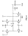
- FIG. 3 The circuit described with reference to FIG. 1 has been perfected in French Patent Application No. 94 05987 by adding a transistor which makes it possible to work with control signals having an amplitude 5 to 10 volts lower than that of the output signals.
- This solution is represented in FIG. 3.
- FIG. 3 there are three transistors MN2, MN1 and MN3 equivalent to the transistors T1, Tp and Td, the two inputs n-1 and n + 1 equivalent to J-1 and J + 1, the two clock inputs ⁇ 1 and ⁇ 2 in phase opposition, the output n of the floor equivalent to the output J as well as the capacities C1, C2, CR respectively corresponding to the capacitors C2, Cb, CI of the embodiment described with reference to FIG.
- a resetting transistor MN4 which connects the node D to a negative voltage Vgoff.
- the gate of transistor MN4 is connected to the node Z itself connected to the output of the next stage n + 1 or to the line n + 2, that is, at the exit line of the next second stage.
- the present invention aims to provide various improvements to the circuits described above.
- the present invention is defined by claim 1.
- the semiconductor devices are constituted by transistors, more particularly transistors MOS and even TFTs.
- the invention is however not limited to this type of transistors.
- the gate of the discharge transistor MN3 is connected from classical way to the n + 1 stage and one of its electrodes connected to the voltage Vh which is chosen at a low level or a high level based of the voltage Vb.
- the embodiment shown in FIG. uses a sixth semiconductor device MN7 connected between the line of output n and the output voltage Vgoff, to keep the output line at a low level.
- this semiconductor device consisting of a MOS transistor has its gate connected to the previous stage n-1 so as to reset the CI capacity to the Vgoff voltage each time you go from stage n-1 on stage n or vice versa.
- the shift register stage described with reference to FIG. 4 has the disadvantage of being sensitive to current leakage through the transistors MN1 or MN3 depending on the direction of operation. Indeed, in the embodiment of FIG. 3, the voltage V- is in general less than the voltage Vgoff so that, in a non-selected stage, the transistor output MN2 has a sufficiently low output current not to load the CI capacity when the clock becomes positive. Typically, for amorphous silicon based transistors, V- ⁇ Vgoff - 2 volts.
- the gate of transistor MN1 is connected to the output line of the previous stage n-1 through a coupling capacitor C5 and a diode-mounted MOS transistor MN5 is connected between the common point between the capacitor C5 and the grid of the transistor MN1 and the point G.
- the discharge transistor MN3 is connected to the next floor n + 1 via a capacitance of coupling C6 and also includes a "clamp" diode consisting of a MN6 transistor.
- the node G is connected to the voltage V1.
- the transistors MN1 and MN3 play a symmetrical role to operate the bi-directional stage.
Description
La présente demande est une demande divisionnaire de la demande EP 97 900 253.2.This application is a divisional application of the application EP 97 900 253.2.
L'invention décrite dans cette demande concerne les registres à décalage utilisant des transistors "MIS" (pour Métal, Isolant, Semiconducteur) de même polarité. Elle concerne plus particulièrement un perfectionnement aux registres à décalage utilisant un nombre limité de transistor "MIS" de même polarité et permettant la sélection des lignes de pixels d'un écran plat.The invention described in this application relates to the registers offset using "MIS" transistors (for Metal, Insulator, Semiconductor) same polarity. It concerns more particularly a improvement to shift registers using a limited number of transistor "MIS" of the same polarity and allowing the selection of the lines of pixels of a flat screen.
Un écran plat, notamment un écran plat à cristaux liquides, est constitué d'un certain nombre de cellules électro-optiques arrangées en lignes et en colonnes commandées chacune par un dispositif de commutation et comportant deux électrodes encadrant un cristal liquide dont les propriétés optiques sont modifiées en fonction de la valeur du champ qui le traverse. L'ensemble constitué par le dispositif de commutation, l'électrode, le cristal liquide, la contre-électrode constitue ce que l'on appelle un "pixel' ou point image. L'adressage de ces pixels s'effectue par l'intermédiaire de lignes de sélection qui commandent l'état passant et non-passant des dispositifs de commutation et de colonnes ou lignes de données qui transmettent, lorsque le dispositif de commutation est passant, une tension appliquée aux bornes des électrodes correspondant au signal de données à afficher, à savoir à une échelle de gris.A flat screen, especially a flat screen LCD, is consisting of a number of electro-optical cells arranged in rows and columns each controlled by a device switching and having two electrodes surrounding a liquid crystal the optical properties are changed according to the value of the field that cross it. The assembly constituted by the switching device, the electrode, the liquid crystal, the counter electrode is what we call a "pixel" or pixel .The addressing of these pixels is done by through selection lines that control the passing state and non-switching devices and columns or lines of data that transmit, when the switching device is passing, a voltage applied across the electrodes corresponding to the signal of data to be displayed, namely on a gray scale.
Selon un mode de réalisation particulièrement avantageux, les électrodes, les dispositifs de commutation, les lignes et les colonnes sont déposées et gravées sur une même plaque substrat de manière à constituer la matrice active de l'écran. Dans ce cas, les circuits de commande périphérique, c'est-à-dire le balayeur de lignes de sélection qui sélectionne les lignes horizontales à afficher et les circuits qui commandent les colonnes peuvent être directement intégrés sur la plaque substrat comportant la matrice active et labriqués en même temps que celle-ci. Ceux-ci imposent donc, notamment lorsque le nombre de pixels est très élevé, d'avoir des circuits de commande les plus petits et les plus simples possible afin d'arriver à un haut degré de rendement de fabrication. Il peut par ailleurs être avantageux d'utiliser des dispositifs semi-conducteurs comme dispositifs de commutation des pixels du même type de conductivité dans tout l'afficheur.According to a particularly advantageous embodiment, the electrodes, switching devices, lines and columns are deposited and engraved on the same substrate plate so as to constitute the active matrix of the screen. In this case, the control circuits device, that is, the selection line scanner that selects the horizontal lines to display and the circuits that control the columns can be directly integrated on the substrate plate comprising the active matrix and made at the same time as this one. These impose therefore, especially when the number of pixels is very high, to have control circuits the smallest and simplest way possible so to achieve a high degree of manufacturing efficiency. It can also be advantageous to use semiconductor devices as switching pixels of the same conductivity type throughout the display.
La commande des dispositifs semi-conducteurs peut être laite par des lignes adressées par un ou plusieurs registres à décalage. Une structure de registre à décalage permettant notamment de répondre aux exigences de simplicité évoquées dans le paragraphe précédent a été décrite dans la demande de brevet internationale WO 92/15992 déposée au nom de THOMSON-LCD. Dans ce cas, un étage d'un registre à décalage comporte six transistors et est alimenté par deux signaux d'horloge ainsi que par deux sources positives et une source négative. Le fonctionnement de ce registre repose sur le lait que la grille du transistor qui commande la sortie de l'étage du registre est laissée flottante et qu'ainsi son potentiel suit, par effet capacitif le potentiel de l'horloge et de la sortie. Cet effet est appelé effet "bootstrap" en langue anglaise. Il permet au moment voulu, la charge complète de la sortie au potentiel le plus élevé de horloge. A ce transistor de sortie sont associés un transistor permettant de précharger ]a grille du transistor de sortie et un transistor permettant de la décharger. D'autre part, le fonctionnement de ces trois transistors est tel que si l'effet "bootstrap" permet une bonne charge des sorties, il s'accompagne d'effets parasites qui nécessitent l'utilisation de trois transistors supplémentaires. Un autre inconvénient réside dans le lait que certains transistors subissent en permanence un stress de grille, à savoir une tension positive sur la grille qui peut avoir pour conséquence une dérive de leur tension de seuil et entraíner à terme un disfonctionnement de l'ensemble du dispositif. The control of the semiconductor devices can be selected by lines addressed by one or more shift registers. A structure shift register, in particular to meet the requirements of simplicity mentioned in the previous paragraph was described in the International Patent Application WO 92/15992 filed in the name of THOMSON-LCD. In this case, a stage of a shift register comprises six transistors and is powered by two clock signals as well as by two positive sources and a negative source. The operation of this register rests on the milk that the gate of the transistor that controls the output of the stage of the register is left floating and that thus its potential follows, by effect capacitive the potential of the clock and the output. This effect is called effect "bootstrap" in English language. It allows at the desired moment, the load complete output at the highest potential clock. At this transistor output are associated with a transistor making it possible to preload the gate of the output transistor and a transistor for discharging it. On the other hand, the operation of these three transistors is such that if the effect "bootstrap" allows a good load of the outputs, it is accompanied by parasitic effects which require the use of three additional transistors. Another disadvantage lies in the milk that some transistors undergo in constant grid stress, ie a positive voltage on the grid that may result in a drift of their threshold voltage and cause eventually a malfunction of the entire device.
Pour remédier aux inconvénients ci-dessus, on a proposé dans la demande de brevet français n° 94 05987 déposée le 17 mai 1994 au nom de THOMSON-LCD des circuits plus simples à trois ou quatre transistors présentant des durées de vie rallongées.To overcome the above disadvantages, it has been proposed in the French Patent Application No. 94 05987 filed May 17, 1994 in the name of THOMSON-LCD simpler circuits with three or four transistors with extended service lives.
Ainsi, comme représenté sur la figure 1 qui correspond à la figure
2 de la demande de brevet français N° 94 05987, un étage 21 d'un registre à
décalage permettant de commander les lignes de sélection est constitué de
trois transistors Tl, Tp et Td. Dans ce cas, le transistor Tl commande le
noeud D de la sortie sur la ligne J. Il est préchargé par le transistor Tp et
déchargé par le transistor Td. De manière plus précise, l'étage 21 est
connecté en 22 à la ligne précédente J-1 par le drain du transistor Tp. La
grille du transistor Tp est connectée à son drain tandis que sa source est
connectée au point G lui-même connecté à la grille du transistor Tl. D'autre
part, le point G est relié à une tension négative V- par l'intermédiaire du
transistor de décharge Td, lui-même commandé par le potentiel de la ligne
J+1 connectée en sortie de l'étage suivant. De plus, le noeud D est connecté
à la source du transistor Tl, au noeud G par l'intermédiaire d'une capacité Cb
et à la ligne J à sélectionner dont la charge est symbolisée électriquement
par une capacité CI reliée à la masse 32. Un signal d'horloge 1 est appliqué
sur le drain du transistor de sortie TI. Il existe entre le drain et la grille de ce
transistor, une capacité parasite Cp responsable de l'effet "bootstrap"
expliqué avec référence à la demande WO92/15992. D'autre part dans ce
schéma, une horloge 2 exactement complémentaire de l'horloge 1 est
connectée au noeud G par l'intermédiaire d'une capacité C2 d'une valeur
équivalente à celle de la capacité parasite Cp.Thus, as shown in Figure 1 which corresponds to the figure
2 of the French patent application No. 94 05987, a
Ainsi les effets parasites, conséquence de l'effet "bootstrap" sont
contre-balancés grâce à la liaison de l'horloge 2 (complémentaire de
l'horloge 1) avec la grille du transistor Tp par l'intermédiaire de la capacité
C2 de valeur Ct équivalente à celle de Cp. Les deux horloges étant
exactement complémentaires, elles n'induisent aucune tension parasite au
noeud G, à savoir sur la grille du transistor Tl. Un circuit équivalent comporte
une capacité CI = 2 x Ct entre le noeud G et la masse 32. Une telle structure
réduisant l'effet « bootstrap », il est nécessaire d'ajouter une capacité
"bootstrap" Cb entre le noeud source D et le noeud grille G afin que la tension
de la grille suive une fraction Cb/(Cb + 2xCp) des variations de la tension de
source. Ainsi, il suffit, pour qu'un ratio de "bootstrap" de 60% soit atteint, que
Cb ait trois fois la valeur de Ct. Le circuit décrit ci-dessus conserve l'effet
"bootstrap" sans ses effets secondaires. La durée de vie du circuit et donc
de l'ensemble du dispositif est rallongée alors que le nombre de transistors
nécessaires a été divisé par deux par rapport à l'art antérieur.Thus the parasitic effects, consequence of the "bootstrap" effect are
counterbalanced thanks to the connection of the clock 2 (complementary to
clock 1) with transistor Tp gate through capacitance
C2 of Ct value equivalent to that of Cp. Both clocks being
exactly complementary, they do not induce any parasitic voltage at
node G, namely on the gate of transistor T1. An equivalent circuit comprises
a capacitance CI = 2 x Ct between the node G and the
Le fonctionnement du circuit est expliqué avec référence aux
chronogrammes 2a à 2f chacun d'eux montrant en abscisse une échelle de
temps et en ordonnée un potentiel. Lorsque l'étage J-1 précédent envoie
une impulsion (figure 2c) en 22, le transistor de précharge Tp est passant et
charge la capacité de "bootstrap" Cb. Le potentiel du noeud G (fig. 2d) monte
jusqu'à celui de la ligne J-1 correspondant à l'étage 5 précédent, auquel if
faut retrancher sensiblement la valeur de la tension de seuil du transistor Tp.
Le transistor TI est alors passant. Lorsque l'horloge 1 monte à son tour (fig.
2a) la sortie J suit, entraínant la grille du transistor Tl grâce à la capacité de
"bootstrap" (fig. 2d). Le transistor Tl est alors largement passant et le noeud
D et la ligne J suivent parfaitement le potentiel de l'horloge 1 (fig. 2e)
jusqu'à sa descente. A ce moment, la ligne suivante J+1 monte (fig. 2f) et
rend passant le transistor Td qui décharge la capacité de "bootstrap" Cb de
sorte que le transistor Tl n'est plus passant pour les coups d'horloge
suivants (fig. 2d).The operation of the circuit is explained with reference to
chronograms 2a to 2f each of them showing on the abscissa a scale of
time and ordinate a potential. When the previous floor J-1 sends
a pulse (FIG. 2c) at 22, the precharge transistor Tp is conducting and
loads the bootstrap capability Cb. The potential of node G (FIG 2d) rises
up to that of line J-1 corresponding to the
Le circuit décrit avec référence à la figure 1 a été perfectionné
dans la demande de brevet français n° 94 05987 en ajoutant un transistor
qui permet de travailler avec des signaux de commande ayant une amplitude
de 5 à 10 volts inférieure à celle des signaux de sortie. Cette solution est
représentée sur la figure 3. Sur cette figure on retrouve trois transistors MN2,
MN1 et MN3 équivalents aux transistors Tl, Tp et Td, les deux entrées n- 1
et n + 1 équivalentes à J- 1 et J + 1, les deux entrées d'horloge 1 et 2 en
opposition de phase, la sortie n de l'étage équivalente à la sortie J ainsi que
les capacités C1, C2, CR correspondant respectivement aux capacités C2,
Cb, CI du mode de réalisation décrit avec référence à la figure 1. Dans ce
cas on prévoit un transistor de remise à zéro MN4 qui connecte le noeud D à
une tension négative Vgoff. La grille du transistor MN4 est connectée au
noeud Z lui-même relié à la sortie de l'étage suivant n + 1 ou à la ligne n + 2,
c'est-à-dire à la ligne de sortie du second étage suivant. Comme décrit dans
la demande française, une telle structure permet une remise à zéro avec un
circuit simplifié. De plus, on a prévu entre la ligne de sortie n et une tension
Vcomp, une capacité de compensation C comp.The circuit described with reference to FIG. 1 has been perfected
in French Patent Application No. 94 05987 by adding a transistor
which makes it possible to work with control signals having an
La présente invention a pour objet d'apporter différents perfectionnements aux circuits décrits ci-dessus.The present invention aims to provide various improvements to the circuits described above.
La présente invention est définie par la revendication 1. The present invention is defined by
D'autres caractéristiques et avantages de la présente invention
apparaítront à la lecture de la description de différents modes de réalisation
faites ci-après avec référence aux dessins ci-annexés dans lesquels :
Pour simplifier la description dans les figures 4 à 5, les mêmes éléments que ceux de la figure 3, déjà décrite, portent les mêmes références.To simplify the description in FIGS. 4 to 5, the same elements that those of Figure 3, already described, bear the same references.
Dans la description qui va suivre, les dispositifs semi-conducteurs sont constitués par des transistors, plus particulièrement des transistors MOS et même des TFT. L'invention n'est toutefois pas limitée à ce type de transistors.In the following description, the semiconductor devices are constituted by transistors, more particularly transistors MOS and even TFTs. The invention is however not limited to this type of transistors.
On décrira avec référence à la figure 4, un mode de réalisation particulier qui permet à l'étage du registre à décalage de la figure 3 de fonctionner de manière bi-directionnelle. Cet étage permet de décaler les informations de l'étage n-1 vers l'étage n + 1 ou de l'étage n + 1 vers l'étage n-1 selon la polarité des tensions Vh et Vb appliquées aux électrodes des transistors MOS MN1 et MN3 utilisés respectivement pour la charge et la décharge du transistor de sortie MN2. Ainsi, comme représenté clairement sur la figure 4, la grille du transistor de précharge MN1 est connectée directement à la sortie de l'étage n-1 et une de ses électrodes connectée à la tension Vb qui peut être choisie à un niveau haut ou à un niveau bas. D'autre part, la grille du transistor de décharge MN3 est connectée de manière classique à l'étage n + 1 et une de ses électrodes connectée à la tension Vh qui est choisie à un niveau bas ou à un niveau haut en fonction de la tension Vb. Dans le mode de réalisation représenté à la figure 4, on utilise un sixième dispositif semi-conducteur MN7 connecté entre la ligne de sortie n et la tension de sortie Vgoff, pour maintenir la ligne de sortie à un niveau bas. Dans ce cas, ce dispositif semi-conducteur constitué par un transistor MOS a sa grille reliée à l'étage précédent n-1 de manière à remettre la capacité CI à la tension Vgoff à chaque fois que l'on passe de l'étage n-1 à l'étage n ou inversement.One embodiment will be described with reference to FIG. particular that allows the shift register stage of Figure 3 to operate bi-directionally. This floor allows you to shift information from floor n-1 to floor n + 1 or floor n + 1 to floor n-1 according to the polarity of the voltages Vh and Vb applied to the electrodes of the MOS MN1 and MN3 transistors used respectively for charging and discharge of the output transistor MN2. So, as clearly represented in FIG. 4, the gate of the precharging transistor MN1 is connected directly at the output of stage n-1 and one of its electrodes connected to the voltage Vb which can be chosen at a high level or at a low level. On the other hand, the gate of the discharge transistor MN3 is connected from classical way to the n + 1 stage and one of its electrodes connected to the voltage Vh which is chosen at a low level or a high level based of the voltage Vb. In the embodiment shown in FIG. uses a sixth semiconductor device MN7 connected between the line of output n and the output voltage Vgoff, to keep the output line at a low level. In this case, this semiconductor device consisting of a MOS transistor has its gate connected to the previous stage n-1 so as to reset the CI capacity to the Vgoff voltage each time you go from stage n-1 on stage n or vice versa.
L'étage du registre à décalage décrit avec référence à la figure 4 présente l'inconvénient d'être sensible aux fuites de courant à travers les transistors MN1 ou MN3 suivant le sens de fonctionnement. En effet, dans le mode de réalisation de la figure 3, la tension V- est en général inférieure à la tension Vgoff de façon à ce que, dans un étage non-sélectionné, le transistor de sortie MN2 ait un courant de sortie suffisamment faible pour ne pas charger la capacité CI quand l'horloge devient positive. Typiquement, pour des transistors à base de silicium amorphe, V- ≤ Vgoff - 2 volts.The shift register stage described with reference to FIG. 4 has the disadvantage of being sensitive to current leakage through the transistors MN1 or MN3 depending on the direction of operation. Indeed, in the embodiment of FIG. 3, the voltage V- is in general less than the voltage Vgoff so that, in a non-selected stage, the transistor output MN2 has a sufficiently low output current not to load the CI capacity when the clock becomes positive. Typically, for amorphous silicon based transistors, V- ≤ Vgoff - 2 volts.
Pour remédier à cet inconvénient, on utilise la solution représentée à la figure 5. Dans ce cas, la grille du transistor MN1 est connectée à la ligne de sortie de l'étage précédent n-1 par l'intermédiaire d'une capacité de couplage C5 et un transistor MOS MN5 monté en diode est connecté entre le point commun entre la capacité C5 et la grille du transistor MN1 et le point G. De même, le transistor de décharge MN3 est connecté à l'étage suivant n+1 par l'intermédiaire d'une capacité de couplage C6 et comporte aussi une diode de "clamp" constituée par un transistor MN6. Dans le mode de réalisation de la figure 5, on voit que le noeud G est relié à la tension V1. En fait, dans les modes de réalisation des figures 4 et 5, les transistors MN1 et MN3 jouent un rôle symétrique permettant de faire fonctionner l'étage de bi-directionnelle.To remedy this drawback, we use the solution represented in FIG. 5. In this case, the gate of transistor MN1 is connected to the output line of the previous stage n-1 through a coupling capacitor C5 and a diode-mounted MOS transistor MN5 is connected between the common point between the capacitor C5 and the grid of the transistor MN1 and the point G. Similarly, the discharge transistor MN3 is connected to the next floor n + 1 via a capacitance of coupling C6 and also includes a "clamp" diode consisting of a MN6 transistor. In the embodiment of Figure 5, it can be seen that the node G is connected to the voltage V1. In fact, in the embodiments of FIGS. 4 and 5, the transistors MN1 and MN3 play a symmetrical role to operate the bi-directional stage.
Il est évident pour l'homme de l'art que les différents perfectionnements décrits ci-dessus peuvent être combinés les uns avec les autres, comme mentionnés dans les revendications ci-après.It is obvious to those skilled in the art that the different The improvements described above can be combined with each other others, as mentioned in the claims below.
Claims (7)
- Shift register containing a plurality of cascaded stages (n-1, n, n+1), each stage (n) containing an output at a first node (D) and being connected to the output of the preceding stage (n-1), to the output of the next stage (n+1) and to means delivering first and second clock signals (1,2), the said stage containing a first semiconductor output device (MN2) switching the output (n) between high and low values of the first clock signal (1), the first semiconductor device being controlled by the potential of a second node (G), itself connected:characterized in that it is connected moreover:to the means delivering the second clock signal (2) across a first capacitance;to a first low or high potential (Vh) across a second semiconductor device (MN3) controlled by the output of the next stage (n+1), andto a second high or low potential (Vb) across a third semiconductor device (MN1) controlled by the output of the preceding stage (n-1).
- Register according to Claim 1, characterized in that it includes a sixth semiconductor device (MN7) connected between the output line and a negative voltage (Vgoff), the sixth semiconductor device being controlled by the output of the preceding stage.
- Register according to either one of Claims 1 and 2, characterized in that the output (n) of the said stage is linked to a negative voltage (Vgoff) across a fourth semiconductor device (MN4) controlled by the output of the next stage (n+1) or of the next but one stage (n+2).
- Register according to any one of Claims 1 to 3, characterized in that:the second node (G) is connected to the voltage (V1)and in that it includes means for latching the control voltage of the second and third semiconductor devices at a value less than or equal to zero.
- Register according to Claim 4, characterized in that the means consist of a capacitance (C5, C6) connected between the control of the said semiconductor device (MN1, MN3) and the node (G), a fifth and sixth semiconductor devices (MN5, MN6) being connected respectively between the control of the second or of the third semiconductor devices and the node (G), the fifth and sixth semiconductor devices (MN5, MN6) being controlled by the voltage (V1) at the node (G).
- Register according to any one of Claims 1 to 5, characterized in that the semiconductor devices consist of MIS transistors, preferably TFT transistors.
- Register according to any one of Claims 1 to 6, characterized in that the clock signals (1,2), are obtained through the same clock signal in phase opposition.
Applications Claiming Priority (3)
| Application Number | Priority Date | Filing Date | Title |
|---|---|---|---|
| FR9600260A FR2743662B1 (en) | 1996-01-11 | 1996-01-11 | IMPROVEMENT IN SHIFT REGISTERS USING TRANSISTORS OF THE SAME POLARITY |
| FR9600260 | 1996-01-11 | ||
| EP97900253A EP0815562B1 (en) | 1996-01-11 | 1997-01-09 | Improvement to shift registers using mis transistors having the same polarity |
Related Parent Applications (1)
| Application Number | Title | Priority Date | Filing Date |
|---|---|---|---|
| EP97900253A Division EP0815562B1 (en) | 1996-01-11 | 1997-01-09 | Improvement to shift registers using mis transistors having the same polarity |
Publications (3)
| Publication Number | Publication Date |
|---|---|
| EP1156491A2 EP1156491A2 (en) | 2001-11-21 |
| EP1156491A3 EP1156491A3 (en) | 2003-11-05 |
| EP1156491B1 true EP1156491B1 (en) | 2005-03-23 |
Family
ID=9488037
Family Applications (1)
| Application Number | Title | Priority Date | Filing Date |
|---|---|---|---|
| EP01119573A Expired - Lifetime EP1156491B1 (en) | 1996-01-11 | 1997-01-09 | Improvements in shift registers using single type "MIS" transistors |
Country Status (4)
| Country | Link |
|---|---|
| EP (1) | EP1156491B1 (en) |
| JP (1) | JP4035548B2 (en) |
| KR (1) | KR100450865B1 (en) |
| DE (2) | DE69713687T2 (en) |
Families Citing this family (14)
| Publication number | Priority date | Publication date | Assignee | Title |
|---|---|---|---|---|
| KR100685307B1 (en) * | 1999-11-05 | 2007-02-22 | 엘지.필립스 엘시디 주식회사 | Shift Register |
| JP3866070B2 (en) * | 2000-10-20 | 2007-01-10 | 株式会社 日立ディスプレイズ | Display device |
| KR100853720B1 (en) * | 2002-06-15 | 2008-08-25 | 삼성전자주식회사 | Shift resister for driving amorphous-silicon thin film transistor gate and liquid crystal display device having the same |
| TW200703224A (en) * | 2005-03-22 | 2007-01-16 | Koninkl Philips Electronics Nv | A shift register circuit |
| WO2007013010A2 (en) * | 2005-07-26 | 2007-02-01 | Koninklijke Philips Electronics N.V. | A multiple input circuit |
| FR2920907B1 (en) * | 2007-09-07 | 2010-04-09 | Thales Sa | CIRCUIT FOR CONTROLLING THE LINES OF A FLAT SCREEN WITH ACTIVE MATRIX. |
| US8587572B2 (en) | 2007-12-28 | 2013-11-19 | Sharp Kabushiki Kaisha | Storage capacitor line drive circuit and display device |
| RU2458460C2 (en) * | 2007-12-28 | 2012-08-10 | Шарп Кабусики Кайся | Semiconductor device and display device |
| CN101849358A (en) | 2007-12-28 | 2010-09-29 | 夏普株式会社 | Semiconductor device and display device |
| US8547368B2 (en) | 2007-12-28 | 2013-10-01 | Sharp Kabushiki Kaisha | Display driving circuit having a memory circuit, display device, and display driving method |
| FR2975213B1 (en) * | 2011-05-10 | 2013-05-10 | Trixell Sas | DEVICE FOR ADDRESSING LINES OF A CONTROL CIRCUIT FOR ACTIVE DETECTION MATRIX |
| CN102800272B (en) * | 2011-05-27 | 2016-07-06 | 凌巨科技股份有限公司 | The drive circuit of display device |
| US9412764B2 (en) | 2012-11-28 | 2016-08-09 | Semiconductor Energy Laboratory Co., Ltd. | Semiconductor device, display device, and electronic device |
| CN103943054B (en) | 2014-01-27 | 2016-07-13 | 上海中航光电子有限公司 | Gate driver circuit, tft array substrate, display floater and display device |
Family Cites Families (2)
| Publication number | Priority date | Publication date | Assignee | Title |
|---|---|---|---|---|
| US5282234A (en) * | 1990-05-18 | 1994-01-25 | Fuji Photo Film Co., Ltd. | Bi-directional shift register useful as scanning registers for active matrix displays and solid state image pick-up devices |
| FR2720185B1 (en) * | 1994-05-17 | 1996-07-05 | Thomson Lcd | Shift register using M.I.S. of the same polarity. |
-
1997
- 1997-01-09 KR KR1019970706365A patent/KR100450865B1/en not_active IP Right Cessation
- 1997-01-09 DE DE69713687T patent/DE69713687T2/en not_active Expired - Lifetime
- 1997-01-09 EP EP01119573A patent/EP1156491B1/en not_active Expired - Lifetime
- 1997-01-09 DE DE69732867T patent/DE69732867T2/en not_active Expired - Lifetime
-
2005
- 2005-11-28 JP JP2005341578A patent/JP4035548B2/en not_active Expired - Lifetime
Also Published As
| Publication number | Publication date |
|---|---|
| DE69713687D1 (en) | 2002-08-08 |
| EP1156491A2 (en) | 2001-11-21 |
| DE69713687T2 (en) | 2003-02-06 |
| EP1156491A3 (en) | 2003-11-05 |
| DE69732867T2 (en) | 2006-04-13 |
| JP4035548B2 (en) | 2008-01-23 |
| KR100450865B1 (en) | 2005-01-13 |
| KR19980702957A (en) | 1998-09-05 |
| JP2006127751A (en) | 2006-05-18 |
| DE69732867D1 (en) | 2005-04-28 |
Similar Documents
| Publication | Publication Date | Title |
|---|---|---|
| EP0815562B1 (en) | Improvement to shift registers using mis transistors having the same polarity | |
| EP0760149B1 (en) | Shift register using mis transistors having the same polarity | |
| EP1156491B1 (en) | Improvements in shift registers using single type "MIS" transistors | |
| EP0586398B1 (en) | Shift register used as selection line scanner for liquid crystal display | |
| KR100470881B1 (en) | Electric circuit | |
| EP0237365B1 (en) | Photo-sensitive device | |
| EP2013863B1 (en) | Organic electroluminescent display | |
| EP0815552B1 (en) | Method for addressing a flat screen using pixel precharging, driver for carrying out the method, and use thereof in large screens | |
| US6600472B1 (en) | Liquid crystal display device | |
| US8139055B2 (en) | Combined image sensor and display device | |
| US9123613B2 (en) | Image sensor and display | |
| EP0825763A2 (en) | High sensitivity image sensor arrays | |
| US5838290A (en) | Display device with photovoltaic converter | |
| KR20030003055A (en) | Shift register and electronic apparatus | |
| US20090072158A1 (en) | Method of detecting x-rays and x-ray detecting apparatus | |
| EP0972282B1 (en) | Device for controlling a matrix display cell | |
| FR2669759A1 (en) | FLAT SCREEN WITH ACTIVE MATRIX. | |
| WO2020165024A1 (en) | Matrix detector with reduced odd/even effect | |
| US7095005B2 (en) | Image reading device for reversing polarity of stored charge in capacitor | |
| FR2615993A1 (en) | METHOD AND DEVICE FOR THE ELIMINATION OF COUPLING IN MATRIX ADDRESSED THIN FILM TRANSISTOR LIQUID CRYSTAL SCREENS | |
| FR2705183A1 (en) | Improved diode addressing structure for addressing a network of transducers. | |
| FR2488016A1 (en) | Thin-film matrix display panel using elementary modules - has each module provided with addressing transistor and power transistor | |
| den Boer | 6.2: A Select Line Driver for the Offset‐Scan‐and‐Hold Dual Select Diode AMLCDs |
Legal Events
| Date | Code | Title | Description |
|---|---|---|---|
| PUAI | Public reference made under article 153(3) epc to a published international application that has entered the european phase |
Free format text: ORIGINAL CODE: 0009012 |
|
| 17P | Request for examination filed |
Effective date: 20010816 |
|
| AC | Divisional application: reference to earlier application |
Ref document number: 815562 Country of ref document: EP |
|
| AK | Designated contracting states |
Kind code of ref document: A2 Designated state(s): DE FR GB IT NL |
|
| PUAL | Search report despatched |
Free format text: ORIGINAL CODE: 0009013 |
|
| AK | Designated contracting states |
Kind code of ref document: A3 Designated state(s): DE FR GB IT NL |
|
| RIC1 | Information provided on ipc code assigned before grant |
Ipc: 7G 09G 3/36 B Ipc: 7G 11C 19/28 A |
|
| GRAP | Despatch of communication of intention to grant a patent |
Free format text: ORIGINAL CODE: EPIDOSNIGR1 |
|
| AKX | Designation fees paid |
Designated state(s): DE FR GB IT NL |
|
| GRAS | Grant fee paid |
Free format text: ORIGINAL CODE: EPIDOSNIGR3 |
|
| RAP1 | Party data changed (applicant data changed or rights of an application transferred) |
Owner name: THALES AVIONICS LCD S.A. |
|
| GRAA | (expected) grant |
Free format text: ORIGINAL CODE: 0009210 |
|
| AC | Divisional application: reference to earlier application |
Ref document number: 0815562 Country of ref document: EP Kind code of ref document: P |
|
| AK | Designated contracting states |
Kind code of ref document: B1 Designated state(s): DE FR GB IT NL |
|
| PG25 | Lapsed in a contracting state [announced via postgrant information from national office to epo] |
Ref country code: NL Free format text: LAPSE BECAUSE OF FAILURE TO SUBMIT A TRANSLATION OF THE DESCRIPTION OR TO PAY THE FEE WITHIN THE PRESCRIBED TIME-LIMIT Effective date: 20050323 Ref country code: IT Free format text: LAPSE BECAUSE OF FAILURE TO SUBMIT A TRANSLATION OF THE DESCRIPTION OR TO PAY THE FEE WITHIN THE PRESCRIBED TIME-LIMIT;WARNING: LAPSES OF ITALIAN PATENTS WITH EFFECTIVE DATE BEFORE 2007 MAY HAVE OCCURRED AT ANY TIME BEFORE 2007. THE CORRECT EFFECTIVE DATE MAY BE DIFFERENT FROM THE ONE RECORDED. Effective date: 20050323 |
|
| REG | Reference to a national code |
Ref country code: GB Ref legal event code: FG4D Free format text: NOT ENGLISH |
|
| REF | Corresponds to: |
Ref document number: 69732867 Country of ref document: DE Date of ref document: 20050428 Kind code of ref document: P |
|
| GBT | Gb: translation of ep patent filed (gb section 77(6)(a)/1977) |
Effective date: 20050420 |
|
| NLV1 | Nl: lapsed or annulled due to failure to fulfill the requirements of art. 29p and 29m of the patents act | ||
| PLBE | No opposition filed within time limit |
Free format text: ORIGINAL CODE: 0009261 |
|
| STAA | Information on the status of an ep patent application or granted ep patent |
Free format text: STATUS: NO OPPOSITION FILED WITHIN TIME LIMIT |
|
| 26N | No opposition filed |
Effective date: 20051227 |
|
| REG | Reference to a national code |
Ref country code: FR Ref legal event code: PLFP Year of fee payment: 20 |
|
| PGFP | Annual fee paid to national office [announced via postgrant information from national office to epo] |
Ref country code: DE Payment date: 20160128 Year of fee payment: 20 |
|
| PGFP | Annual fee paid to national office [announced via postgrant information from national office to epo] |
Ref country code: FR Payment date: 20160128 Year of fee payment: 20 Ref country code: GB Payment date: 20160201 Year of fee payment: 20 |
|
| REG | Reference to a national code |
Ref country code: DE Ref legal event code: R071 Ref document number: 69732867 Country of ref document: DE |
|
| REG | Reference to a national code |
Ref country code: GB Ref legal event code: PE20 Expiry date: 20170108 |
|
| PG25 | Lapsed in a contracting state [announced via postgrant information from national office to epo] |
Ref country code: GB Free format text: LAPSE BECAUSE OF EXPIRATION OF PROTECTION Effective date: 20170108 |