EP2012375A2 - Organic light emitting device - Google Patents
Organic light emitting device Download PDFInfo
- Publication number
- EP2012375A2 EP2012375A2 EP08252271A EP08252271A EP2012375A2 EP 2012375 A2 EP2012375 A2 EP 2012375A2 EP 08252271 A EP08252271 A EP 08252271A EP 08252271 A EP08252271 A EP 08252271A EP 2012375 A2 EP2012375 A2 EP 2012375A2
- Authority
- EP
- European Patent Office
- Prior art keywords
- layer
- light emitting
- organic light
- emitting device
- metal
- Prior art date
- Legal status (The legal status is an assumption and is not a legal conclusion. Google has not performed a legal analysis and makes no representation as to the accuracy of the status listed.)
- Granted
Links
Images





Classifications
-
- H—ELECTRICITY
- H05—ELECTRIC TECHNIQUES NOT OTHERWISE PROVIDED FOR
- H05B—ELECTRIC HEATING; ELECTRIC LIGHT SOURCES NOT OTHERWISE PROVIDED FOR; CIRCUIT ARRANGEMENTS FOR ELECTRIC LIGHT SOURCES, IN GENERAL
- H05B33/00—Electroluminescent light sources
- H05B33/12—Light sources with substantially two-dimensional [2D] radiating surfaces
- H05B33/26—Light sources with substantially two-dimensional [2D] radiating surfaces characterised by the composition or arrangement of the conductive material used as an electrode
-
- H—ELECTRICITY
- H10—SEMICONDUCTOR DEVICES; ELECTRIC SOLID-STATE DEVICES NOT OTHERWISE PROVIDED FOR
- H10K—ORGANIC ELECTRIC SOLID-STATE DEVICES
- H10K59/00—Integrated devices, or assemblies of multiple devices, comprising at least one organic light-emitting element covered by group H10K50/00
- H10K59/80—Constructional details
- H10K59/805—Electrodes
- H10K59/8052—Cathodes
- H10K59/80524—Transparent cathodes, e.g. comprising thin metal layers
-
- H—ELECTRICITY
- H05—ELECTRIC TECHNIQUES NOT OTHERWISE PROVIDED FOR
- H05B—ELECTRIC HEATING; ELECTRIC LIGHT SOURCES NOT OTHERWISE PROVIDED FOR; CIRCUIT ARRANGEMENTS FOR ELECTRIC LIGHT SOURCES, IN GENERAL
- H05B33/00—Electroluminescent light sources
- H05B33/12—Light sources with substantially two-dimensional [2D] radiating surfaces
- H05B33/22—Light sources with substantially two-dimensional [2D] radiating surfaces characterised by the chemical or physical composition or the arrangement of auxiliary dielectric or reflective layers
-
- H—ELECTRICITY
- H10—SEMICONDUCTOR DEVICES; ELECTRIC SOLID-STATE DEVICES NOT OTHERWISE PROVIDED FOR
- H10K—ORGANIC ELECTRIC SOLID-STATE DEVICES
- H10K50/00—Organic light-emitting devices
- H10K50/80—Constructional details
- H10K50/805—Electrodes
- H10K50/82—Cathodes
- H10K50/828—Transparent cathodes, e.g. comprising thin metal layers
-
- Y—GENERAL TAGGING OF NEW TECHNOLOGICAL DEVELOPMENTS; GENERAL TAGGING OF CROSS-SECTIONAL TECHNOLOGIES SPANNING OVER SEVERAL SECTIONS OF THE IPC; TECHNICAL SUBJECTS COVERED BY FORMER USPC CROSS-REFERENCE ART COLLECTIONS [XRACs] AND DIGESTS
- Y10—TECHNICAL SUBJECTS COVERED BY FORMER USPC
- Y10S—TECHNICAL SUBJECTS COVERED BY FORMER USPC CROSS-REFERENCE ART COLLECTIONS [XRACs] AND DIGESTS
- Y10S428/00—Stock material or miscellaneous articles
- Y10S428/917—Electroluminescent
Definitions
- the present invention relates to an organic light emitting device, and more particularly, to an organic light emitting device including a cathode that has high light transmittance.
- Organic light emitting devices which are self-emitting devices, have high brightness compared to liquid crystal display devices and can also be thinner than liquid crystal display devices because they do not use backlight units.
- An organic light emitting device has a structure that includes an anode, an organic layer, and a cathode, which are sequentially stacked on a substrate on which pixel circuits are arranged and can be embodied as, for example, thin film transistors.
- Organic light emitting devices can be classified into two emission types according to the direction of light emission. These are a top emission type and a bottom emission type. In a top emission type organic light emitting device, light is emitted to form an image in a direction away from a substrate on which the organic light emitting device is disposed, that is, towards a cathode.
- the top emission type organic light emitting device can have a high aperture ratio compared to a bottom emission type organic light emitting device in which light is emitted to form an image in a direction towards the substrate, thereby having high light transmittance.
- the cathode which is formed on the top of the organic light emitting device, needs to be transparent, the improvement of transparency of the cathode is limited. That is, while the cathode needs to have lower work function than the anode, a material having a low work function, such as a metal, generally has low light transmittance.
- a conventional transparent cathode is formed of a thin film of a metal having a low work function.
- the metal since the metal has a low light transmittance, improvement of light transmittance is limited.
- the thickness of the organic layers interposed between the anode and the cathode will vary. That is, since light is emitted by exitons formed by recombination of holes injected from the anode and electrons injected from the cathode in the organic light emitting layer, the thicknesses of the organic layers, particularly of a hole or electron injection layer, or a hole or electron transport layer, have been varied to control distances from exitons and resonance for each color.
- An independent mask is required for each color to vary the thicknesses of the deposited organic layers.
- independent deposition has the disadvantages of further complicating processes and increasing costs for the manufacturing process.
- the thickness of the organic layers cannot be determined simply by optical efficiency since electrical characteristics of the device may worsen when the thickness of the hole layer or the electron layer varies.
- An aspect of an embodiment of the present invention is directed toward a top emission type organic light emitting device having high light transmittance without the need for a resonance structure when light for forming an image is emitted in a direction toward a cathode.
- An embodiment of the present invention provides an organic light emitting device including: an anode including an anode material and for injecting holes; an organic layer including a light emitting layer on the anode; and a cathode on the organic layer and through which light emitted from the light emitting layer passes, wherein the cathode includes: a buffer layer, a metal oxide layer including a metal oxide, and a metal layer including a metal having an absolute work function value lower than an absolute work function value of the anode material and coupled to the buffer layer and the metal oxide layer.
- the metal oxide layer may include a material selected from the group consisting of an indium oxide, an indium tin oxide, a zinc oxide, an indium zinc oxide, SnO 2 , AZO, Ca 12 Al 7 O x , and combinations thereof.
- the metal layer may include a metal having a work function in the range from about 1 to about 4.5 eV.
- the metal layer may include a metal selected from the group consisting of Ag, Mg, Al, Pt, Pd, Au, Ni, Nd, Ir, Cr, Ca, In, and combinations thereof.
- a thickness of the metal layer may be in the range from about 50 to about 150 x 10 -10 m.
- the buffer layer may include an organic dipole material.
- the buffer layer may include a material selected from the group consisting of fullerene, a metal-containing fullerene-based complex, carbon nanotube, carbon fiber, carbon black, graphite, carbyne, MgC 60 , SrC 60 , CaC 60 , C 60 , C 70 , MgO, YbO, and combinations thereof.
- a thickness of the buffer layer may be less than about 20 x 10 -10 m.
- the cathode may have at least about 85% light transmittance.
- the cathode may have resistance in the range from about 0.001 to about 1000 ⁇ / ⁇ .
- the cathode may have a work function in the range from about 1 to about 6 eV.
- the organic light emitting device may further include an electron injection layer between the buffer layer and the metal layer.
- the electron injection layer may include a material selected from the group consisting of BaF 2 , LiF, NaF, MgF 2 , AlF 3 , CaF 2 , NaCl, CsF, Li 2 O, BaO, Liq, and combinations thereof.
- a thickness of the electron injection layer may be less than about 10x10' 10 m.
- the organic light emitting device may further include an intermediate layer between the metal layer and the metal oxide layer.
- the intermediate layer may include a metal having a work function in the range from about 1 to about 5 eV or an alloy formed of at least two metals.
- the intermediate layer may include a metal selected from the group consisting of In, Ag, Al, Ca, Mg, and combinations thereof.
- a thickness of the intermediate layer may be in the range from about 1 to about 200 x 10 -10 m.
- the anode may further include a reflective layer.
- the reflective layer may include a material selected from the group consisting of Ag, Mg, Al, Pt, Pd, Au, Ni, Nd, Ir, Cr, and combinations thereof.
- the anode material may include a material selected from the group consisting of an indium oxide, an indium tin oxide, a zinc oxide, an indium zinc oxide, and combinations thereof.
- an organic light emitting device including: an anode including an anode material and for injecting holes; an organic light emitting layer on the anode; a buffer layer on the organic light emitting layer; a metal layer including a metal having an absolute work function value lower than an absolute work function value of the anode material, the metal layer being on the buffer layer; and a metal oxide layer including a metal oxide on the metal layer.
- the metal oxide layer may include a material selected from the group consisting of an indium oxide, indium tin oxide, zinc oxide, indium zinc oxide, SnO 2 , AZO, Ca 12 Al 7 O x , and combinations thereof.
- the metal layer may include a metal having a work function in the range from about 1 to about 4.5 eV.
- the metal layer may include a metal selected from the group consisting of Ag, Mg, Al, Pt, Pd, Au, Ni, Nd, Ir, Cr, Ca, In, and combinations thereof.
- a thickness of the metal layer may be in the range from about 60 to about 150 x 10 -10 m.
- the buffer layer may include an organic dipole material.
- the buffer layer may include a material selected from the group consisting of fullerene, a metal-containing fullerene-based complex, carbon nanotube, carbon fiber, carbon black, graphite, carbyne, MgC 60 , SrC 60 , CaC 60 , C 60 , C 70 , MgO, YbO, and combinations thereof.
- a thickness of the buffer layer may be less than about 20 x 10 -10 m.
- the organic light emitting device may further include an electron injection layer between the buffer layer and the metal layer.
- the electron injection layer may include a material selected from the group consisting of BaF 2 , LiF, NaF, MgF 2 , AlF 3 , CaF 2 , NaCl, CsF, Li 2 O, BaO, Liq, and combinations thereof.
- a thickness of the electron injection layer may be less than about 10 x10 -10 m.
- the organic light emitting device may further include an intermediate layer between the metal layer and the metal oxide layer.
- the intermediate layer may include a metal having a work function in the range from about 1 to about 5 eV or an alloy formed of at least two metals.
- the intermediate layer may include a metal selected from the group consisting of In, Ag, Al, Ca, Mg, and combinations thereof.
- a thickness of the intermediate layer may be in the range from about 1 to about 200 x 10 -10 m.
- the anode may further include a reflective layer.
- the reflective layer may include a material selected from the group consisting of Ag, Mg, Al, Pt, Pd, Au, Ni, Nd, Ir, Cr, and combinations thereof.
- the anode material may include a material selected from the group consisting of an indium oxide, an indium tin oxide, a zinc oxide, an indium zinc oxide, and combinations thereof.
- an organic light emitting device including: an anode including an anode material and for injecting holes; an organic layer including a light emitting layer on the anode; and a cathode on the organic layer through which light emitted from the light emitting layer passes, wherein the cathode includes: a metal oxide layer including a metal oxide, and a complex layer coupled to the metal oxide layer and comprising a buffer material and a metal having an absolute work function value lower than an absolute work function value of the anode material.
- the metal oxide layer may include a material selected from the group consisting of an indium oxide, an indium tin oxide, a zinc oxide, an indium zinc oxide, SnO 2 , AZO, Ca 12 Al 7 O X , and combinations thereof.
- the metal may have a work function in the range from about 1 to about 4.5 eV.
- the metal may be selected from the group consisting of Ag, Mg, Al, Pt, Pd, Au, Ni, Nd, Ir, Cr, Ca, In, and combinations thereof.
- the buffer material may include an organic dipole material.
- the buffer material may include a material selected from the group consisting of fullerene, a metal-containing fullerene-based complex, carbon nanotube, carbon fiber, carbon black, graphite, carbyne, MgC 60 , SrC 60 , CaC 60 , C 60 , C 70 , MgO, YbO, and combinations thereof.
- a thickness of the complex layer may be in the range from about 60 to about 170 x 10 -10 m.
- the organic light emitting device may further include an intermediate layer between the complex layer and the metal oxide layer.
- the intermediate layer may include a metal having a work function in the range from about 1 to about 5 eV or an alloy formed of at least two metals.
- the intermediate layer may include a metal selected from the group consisting of In, Ag, Al, Ca, Mg, and combinations thereof.
- a thickness of the intermediate layer may be in the range from about 1 to about 200 x 10 -10 m.
- the anode may further comprise a reflective layer.
- the reflective layer may include a material selected from the group consisting of Ag, Mg, Al, Pt, Pd, Au, Ni, Nd, Ir, Cr, and combinations thereof.
- the anode material may include a material selected from the group consisting of an indium oxide, indium tin oxide, zinc oxide, indium zinc oxide, and combinations thereof.
- An aspect of the invention provides an organic light emitting device ase set out in Claim 1.
- Preferred featurs of the invention are set out in Claims 2 to 24.
- FIG. 1 shows a schematic cross-sectional view of an organic light emitting device according to an embodiment of the present invention
- FIG. 2 shows a schematic cross-sectional view of an organic light emitting device according to another embodiment of the present invention
- FIG. 3 shows a schematic cross-sectional view of an organic light emitting device according to another embodiment of the present invention.
- FIG. 4 shows a schematic cross-sectional view of an organic light emitting device according to another embodiment of the present invention.
- FIG. 5 shows a schematic cross-sectional view of an organic light emitting device according to another embodiment of the present invention.
- FIG. 6 shows a schematic cross-sectional view of an organic light emitting device according to another embodiment of the present invention.
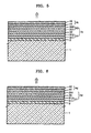
- FIG. 7 shows a cross-sectional view of an anode of an organic light emitting device according to an embodiment of the present invention
- FIG. 8 shows a cross-sectional view of an anode of an organic light emitting device according to another embodiment of the present invention.
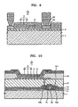
- FIG. 9 shows a cross-sectional view of a passive matrix type organic light emitting display device to which an organic light emitting device of FIG. 1 is applied;
- FIG. 10 shows a cross-sectional view of an active matrix type organic light emitting display device to which an organic light emitting device of FIG. 1 is applied;
- FIG. 11 shows a graph illustrating current density characteristics of organic light emitting devices prepared according to Preparation Examples 1 to 4.
- FIG. 12 shows a graph illustrating current density characteristics of organic light emitting devices prepared according to Comparative Example 1 and Example 1.
- FIG. 1 shows a schematic cross-sectional view of an organic light emitting device according to an embodiment of the present invention.
- the organic light emitting device includes an anode 2, an organic layer 3 and a cathode 4 sequentially stacked on a substrate 1.
- holes injected from the anode 2 and electrons injected from the cathode 4 combine to generate light in the organic layer 3.
- the light generated in the organic layer 3 is emitted towards the cathode 4, i.e., in the direction of the arrow shown on FIG. 1 , and an image is formed in an upward direction from the cathode 4.
- This is referred to as a top emission type structure.
- the cathode 4 includes a buffer layer 43, a metal layer 41, and a metal oxide layer 42, which are sequentially stacked on the organic layer 3.
- the substrate 1 may be formed of a glass material, a plastic material, or a metal material.
- a pixel circuit, in which a thin film transistor and a capacitor may be combined, can be disposed on the substrate 1.
- the anode 2 formed on the substrate 1 is connected to an external power source and provides holes to the organic layer 3.
- the anode 2 may include a material having a relatively high absolute work function value, such as an indium oxide (InO), an indium tin oxide (ITO), a zinc oxide (ZnO) and/or an indium zinc oxide (IZO).
- the cathode 4 is connected to an external power source and provides electrons to the organic layer 3.
- the cathode 4 may include a metal layer 41 composed of a metal having a lower absolute work function value than the material forming the anode 2.
- the work function of the metal forming the metal layer 41 may be in the range from about 1 to about 4.5 eV (or from 1 to 4.5 eV), and, in one embodiment, in the range from about 2 to about 4.2 eV (or from 2 to 4.2 eV), but is not limited thereto.
- the work function may be chosen based on the anode 2.
- the metal layer 41 may include Ag, Mg, Al, Pt, Pd, Au, Ni, Nd, Ir, Cr, Ca and/or In, but is not limited thereto.
- the metal layer 41 functions as a layer for controlling (or lowering) the work function with respect to the anode 2.
- the thickness of the metal layer 41 should be minimized.
- the thickness of the metal layer 41 may be in the range from about 50 to about 150 x 10 -10 m (or from 50 to 150 x 10- -10 m), and, in one embodiment, in the range from about 60 to about 80 x 10 -10 m (or 60 to 80 x 10 -10 m), but is not limited thereto.
- the thickness of the metal layer 41 can be adjusted within the range described above in consideration of light transmittance and resistance characteristics of the cathode 4.
- a metal oxide layer 42 is formed as an auxiliary electrode on the metal layer 41.
- the material forming the metal oxide layer 42 may have a relatively high work function to facilitate the injection of electrons (e.g., to the organic layer).
- a material having a work function in the range from about 2 to about 4.5 eV (or from 2 to 4.5 eV), and, in one embodiment, in the range from about 2.5 to about 4.5 eV (or from 2.5 to 4.5 eV), may be used, but is not limited thereto.
- the metal oxide layer 42 may include a material having a relatively high transmittance and conductivity, such as an indium oxide, an indium tin oxide, a zinc oxide, an indium zinc oxide, and/or SnO 2 , AZO, Ca 12 Al 7 O x .
- the thickness of the metal oxide layer 42 may be in the range from about 100 to about 3000 x 10 -10 m (or from 100 to 3000 x 10 -10 m).
- the cathode 4 formed of the metal layer 41 and the metal oxide layer 42, has a low light transmittance as described in the background of the invention, optical resonance using micro-cavity structures has conventionally been used.
- electron injection efficiency can be increased by interposing a buffer layer 43, including a buffer material, between the organic layer 3 and the metal layer 41.
- the buffer layer 43 may be a dipole material.
- a buffer layer 43 of an organic dipole material attracts (or pulls) electrons. That is, when an electric field is applied to the cathode 4, particularly to the metal layer 41, the molecules of the buffer layer 43 have a positive polarity at one end and a negative polarity at the other end, and electrons can be injected. Thus, the combination of holes and electrons can be facilitated.
- light emitting efficiency can be increased without using a micro-cavity structure. Accordingly, light emitting efficiency can be improved while forming an image.
- a process for making the top emission type light emitting structure can be simplified by forming the buffer layer 43.
- the buffer layer 43 may include a carbonaceous compound. Further, the buffer layer 43 may be fullerene, a metal-containing fullerene-based complex, carbon nanotube, carbon fiber, carbon black, graphite, carbyne, MgC 60 , SrC 60 , CaC 60 , C 60 , C 70 , MgO and/or YbO, but is not limited thereto.
- the thickness of the buffer layer 43 may be less than about 20 x 10 -10 m (or 20 x 10 -10 m) and, in one embodiment, in the range from about 5 to about 20 x 10 -10 m (or from 5 to 20 x 10 -10 m). When the buffer layer 43 has a thickness within (or substantially within) this range, light transmittance and resistance characteristics of the cathode 4 can be improved.
- the cathode 4 may have light transmittance of greater than about 85% (or 85%), and, in one embodiment, greater than about 90% (or 90%). Thus, the device, including the cathode 4, may have suitable light transmittance.
- the cathode has resistance in the range from about 0.001 to about 1000 ⁇ / ⁇ (or from 0.001 to 1000 ⁇ / ⁇ ), and, in one embodiment, in the range from about 0.001 to about 100 ⁇ / ⁇ (or from 0.001 to 100 ⁇ / ⁇ ).
- the cathode 4 may have suitable conductivity.
- the cathode 4 may also have a work function in the range from about 1.0 to about 6.0 eV (or from 1.0 to 6.0 eV), and, in one embodiment, in the range from about 2.0 to about 5.0 eV (or from 2.0 to 5.0 eV).
- the cathode 4 may have suitable electron injecting capability. Therefore, an organic light emitting device including the cathode 4 may have suitable light emitting efficiency.
- FIG. 2 shows the organic layer 3 of the organic light emitting device of FIG. 1 in more detail.
- the organic layer 3 includes a light emitting layer 32.
- a hole injection-transport layer 31 is interposed between the light emitting layer 32 and the anode 2
- an electron injection-transport layer 33 is interposed between the light emitting layer 32 and the cathode 4.
- the amount of dopant may be in the range from about 0.1 to about 20 parts by weight (or from 0.1 to 20 parts by weight), and, in one embodiment, in the range from about 0.5 to about 12 parts by weight (or from 0.5 to 12 parts by weight) based on 100 parts by weight of the material forming the light emitting layer, that is, based on 100 parts by weight of the total weight of the host and the dopant.
- concentration quenching can be substantially inhibited.
- the light emitting layer 32 may also include a poly(phenylenevinylene) (PPV) based polymer or a derivative thereof, a polyphenylene (PPP) based polymer or a derivative thereof, a polythiophene (PT) based polymer or a derivative thereof, a polyfluorene (PF) based polymer or derivatives thereof and/or a polyspirofluorene (PSF) based polymer or derivatives thereof.
- PPV poly(phenylenevinylene)
- PPPP polyphenylene
- PT polythiophene
- PF polyfluorene
- PSF polyspirofluorene
- the hole injection-transport layer 31 may have a structure in which a hole injection layer (HIL) 311 and a hole transport layer (HTL) 312 are stacked on the anode 2.
- HIL hole injection layer
- HTL hole transport layer
- FIG. 2 shows a structure having both layers, but the hole injection-transport layer 31 may include at least one of the layers.
- known hole injection materials and/or hole transport materials can be used.
- a material forming the HIL 311 is not limited, and may be copper phthalocyanine (CuPc), a star-burst type amine derivative such as TCTA and m-MTDATA, a soluble and conductive polymer such as polyaniline/dodecylbenzenesulfonic acid (Pani/DBSA), poly(3,4-ethylenedioxythiophene)/poly(4-styrenesulfonate) (PEDOT/PSS), and polyaniline/camphor sulfonic acid (Pani/CSA) or (polyaniline)/poly(4-styrenesulfonate) (PANI/PSS).
- CuPc copper phthalocyanine
- DBSA polyaniline/dodecylbenzenesulfonic acid
- PEDOT/PSS poly(3,4-ethylenedioxythiophene)/poly(4-styrenesulfonate)
- Pani/CSA polyaniline/cam
- the thickness of the HIL 311 may be in the range from about 100 to about 10,000 x 10 -10 m (or from 100 to 10,000 x 10 -10 m), and, in one embodiment, in the range from about 100 to about 1000 x 10 -10 m (or from 100 to 1000 x 10 -10 m). When the thickness of the HIL 311 is within (or substantially within) this range, suitable hole injection can be obtained, and an increase in driving voltage can be substantially inhibited.
- the material forming the HTL 312 is not limited, and may include a compound having an arylamine group and/or a carbazole group transporting holes, a phthalocyanine compound and/or a triphenylene derivative.
- the hole transport layer 312 may include 1,3,5-tricarbazolylbenzene, 4,4'-biscarbazolylbiphenyl, polyvinylcarbazol, m-biscarbazolylbenzene, 4,4'-biscarbazolyl-2,2'-dimethylbiphenyl, 4,4',4"-tri(N-carbazolyl)triphenylamine, 1,3,5-tri(2-carbazolylphenyl)benzene, 1,3,5-tris(2-carbazolyl-5-methoxyphenyl)benzene, bis(4-carbazolylphenyl)silane, N,N'-bis(3-methylphenyl)-N,N'-diphenyl-[1,
- the thickness of the HTL 312 is in the range from about 50 to about 1000 x 10 -10 m (or from 50 to 1000 x 10 -10 m), and, in one embodiment, in the range from about 100 to about 600 x 10 -10 m (or from 100 to 600 x 10 -10 m). When the thickness of the HTL 312 is within this range, suitable hole transport properties can be obtained, and an increase in driving voltage can be substantially inhibited.
- the hole injection-transport layer 31 may further include an electron blocking layer (EBL) to extend the lifetime of the organic light emitting device.
- EBL electron blocking layer
- a hole blocking layer may also be formed on the light emitting layer 32 to prevent (or block) triplet exitons or holes from being diffused to the electron transport layer 331 when the light emitting layer 32 includes a phosphorescent dopant.
- the material forming the HBL is not limited, and may be a known HBL material.
- the HBL may include an oxadiazole derivative, a triazole derivative, a phenanthroline derivative, or a hole blocking material disclosed in JP 11-329734(A1 ), Balq, BCP, or the like.
- the thickness of the HBL is in the range from about 50 to about 1000 x 10 -10 m (or from 50 to 1000 x 10 -10 m), and, in one embodiment, in the range from about 100 to about 300 x 10 -10 m (or from 100 to 300 x 10 -10 m). When the thickness of the HBL is within (or substantially within) this range, relatively high hole transport properties can be obtained, and an increase in driving voltage can be substantially inhibited.
- the electron injection-transport layer 33 may include an electron injection layer (EIL) 332 and an electron transport layer (ETL) 331. As shown in FIG. 2 , the electron injection-transport layer 33 may have a structure in which both layers are stacked or a structure having one of the layers. Here, a material that is commonly used to form an electron injection-transport layer in organic light emitting devices can be used.
- EIL electron injection layer
- ETL electron transport layer
- the ETL 331 is formed (e.g., on or over the light emitting layer 32) using vacuum deposition or spin coating.
- the material is not limited, and may include tris(8-hydroxyquinoline)aluminum (Alq 3 ), TAZ, and bis(10-hydroxybenzo[h]quinolinato)beryllium (Bebq2).
- An electron injection layer 332 may be formed on the electron transport layer 331 using vacuum deposition or spin coating.
- the electron injection layer 332 may be BaF 2 , LiF, NaF, MgF 2 , AlF 3 , CaF 2 , NaCl, CsF, Li 2 O, BaO, Liq, or the like, but is not limited thereto.
- FIG. 3 shows a schematic cross-sectional view of an organic light emitting device including a cathode 4a and an organic layer 3a according to another embodiment of the present invention.
- the buffer layer 43 When the buffer layer 43 is included, the structure can be simplified since the same level of light emitting efficiency can be obtained when the electron injection-transport layer includes only the ETL 331 without the electron injection layer as shown in FIG. 3 .
- FIG. 4 shows a schematic cross-sectional view of an organic light emitting device including a cathode 4b and an organic layer 3b according to another embodiment of the present invention.
- the anode 2 is formed on the substrate 1, and the hole injection-transport layer 31 including the hole injection layer 311 and the hole transport layer 312 is formed on the anode 2.
- the light emitting layer 32 is formed on the hole injection-transport layer 31, and the electron transport layer 331 is formed on the light emitting layer 32.
- the buffer layer 43 is formed on the electron transport layer 331, and the electron injection layer 332 is formed on the buffer layer 43. Then, the metal layer 41 and the metal oxide layer 42 are sequentially formed on the electron injection layer 332.
- the thickness of the electron injection layer 332 is less than about 10x10' 10 m (or 10 x 10 -10 m),and, in one embodiment, in the range from about 3 to about 10 x 10 -10 m (or from 3 to 10 x 10 -10 m). When the thickness of the electron injection layer 332 is within (or substantially within) this range, light transmittance and resistance characteristics of the cathode 4b can be improved.
- the ratio of the work function of the anode 2 to that of the cathode 4b can be adjusted by the metal layer 41, and the metal oxide layer 42 compensates for the conductivity of the metal layer 41. Since the buffer layer 43 is interposed between the electron injection layer 332 and the electron transport layer 331, light emitting efficiency can be increased without using a micro-cavity structure.
- An intermediate layer may also be interposed between the metal layer 41 and the metal oxide layer 42.
- the intermediate layer may improve ohmic contact between the metal layer 41 and the metal oxide layer 42.
- the intermediate layer may include a material having a work function in the range from about 1.0 to about 5.0 eV (or from 1.0 to 5.0 eV), and, in one embodiment, in the range from about 2.0 to about 3.5 eV (or from 2.0 to 3.5 eV).
- the intermediate layer may include In, Ag, Al, Ca and/or Mg, but is not limited thereto.
- the thickness of the intermediate layer may be in the range from about 1 to about 200 x 10 -10 m (or from 1 to 200 x 10 -10 m), and, in one embodiment, in the range from about 40 to about 100 x 10 -10 m (or from 40 to 100 x 10 -10 m). When the thickness of the intermediate layer is within (or substantially within) this range, light transmittance and resistance characteristics of the cathode 4 can be improved.
- FIG. 5 shows a schematic cross-sectional view of an organic light emitting device including a cathode 4c and an organic layer 3c according to another embodiment of the present invention.
- the anode 2 is formed on the substrate 1, and the hole injection-transport layer 31, including the HIL 311 and the HTL 312, is formed on the anode 2.
- the light emitting layer 32 is formed on the hole injection-transport layer 31 and the electron injection-transport layer 33, including the ETL 331 and the EIL 332, is formed on the light emitting layer 32.
- a complex layer 44 including a buffer material and a metal, is formed on the electron injection-transport layer 33.
- the complex layer 44 can be formed by co-depositing the buffer material and the metal.
- the buffer material is identical (or substantially identical) to the material used to form the buffer layer 43 described above, and the metal is identical (or substantially identical) to the material used to form the metal layer 41.
- the thickness of the complex layer 44 may be in the range from about 60 to about 120 x 10 -10 m (or from 60 to 120 x 10 -10 m). When the thickness of the complex layer 44 is within (or substantially within) this range, light transmittance and resistance characteristics of a cathode 4c can be improved, thereby increasing light emitting efficiency.
- FIG. 6 shows a schematic cross-sectional view of an organic light emitting device including a cathode 4d and an organic layer 3d according to another embodiment of the present invention.
- the complex layer 44 is included, the EIL 332 need not be included, as shown in FIG. 6 .
- an intermediate layer may further be interposed between the metal oxide layer 42 and the complex layer 44.
- the intermediate layer may improve ohmic contact between the metal oxide layer 42 and the complex layer 44.
- the intermediate layer may include a material having a work function in the range from about 1.0 to about 5.0 eV (or from 1.0 to 5.0 eV), and, in one embodiment, in the range from about 2.0 to about 3.5 eV (or from 2.0 to 3.5 eV).
- the intermediate layer may include In, Ag, Al, Ca and/or Mg, but is not limited thereto.
- the thickness of the intermediate layer may be in the range from about 1 to about 200 x 10 -10 m (or from 1 to 200 x 10 -10 m), and, in one embodiment, in the range from about 40 to about 100 x 10 -10 m (or from 40 to 100 x 10 -10 m). When the thickness of the intermediate layer is within this range, light transmittance and resistance characteristics of the cathode 4 can be improved.
- the anode 2 may include a reflective layer 22 on the substrate 1 and an anode material layer 21 on the reflective layer 22 which injects holes into the hole injection-transport layer 31, as shown in FIG. 7 .
- the anode material layer 21 may include a material having a sufficiently high work function selected from indium oxide (InO), an indium tin oxide (ITO), a zinc oxide (ZnO), and an indium zinc oxide (IZO).
- InO indium oxide
- ITO indium tin oxide
- ZnO zinc oxide
- IZO indium zinc oxide
- the reflective layer 22 may include a material having high light reflectivity selected from Ag, Mg, Al, Pt, Pd, Au, Ni, Nd, Ir, Cr and compounds thereof.
- FIG. 8 shows a schematic cross-sectional view of an organic light emitting device including an anode 2a according to another embodiment of the present invention.
- the anode 2 may have a sandwich structure as shown in FIG. 8 with a layer 23 formed of the same (or substantially the same) material as the anode material layer 21 being disposed under the reflective layer 22.
- the anode 2 is formed in a stripe pattern on the substrate 1, and an inner insulating layer 24 is formed on the anode 2.
- a separator 25 crosses the anode 2 at right angles on the inner insulating layer 24 to pattern the organic layer 3 and the cathode 4.
- the organic layer 3 and the cathode 4 are patterned by the separator 25 to cross the anode 2.
- a sealing member (not shown) is formed on the anode 2 to isolate the organic light emitting device from the air.
- the organic layer 3 and the cathode 4 can be formed through a patterned mask without using the separator 25.
- Light extraction efficiency can be increased without using a micro-cavity structure in a PM organic light emitting display device, and, accordingly, an appropriate level of light emitting efficiency can be obtained.
- a pixel circuit including a thin film transistor (TFT) is on the substrate 1.
- the pixel circuit includes at least one TFT and the TFT is electrically connected to the organic light emitting device.
- the buffer layer 11 is on the substrate 1, and a semiconductor active layer 12 having a pattern (that may be predetermined) is on the buffer layer 11.
- a gate insulating layer 13 formed of SiO 2 , SiNx, or the like is on the active layer 12, and a gate electrode 14 is on a part of the gate insulating layer 13.
- the gate electrode 14 is connected to a gate line, which applies on/off signals to a TFT.
- An interlayer dielectric layer 15 is on the gate electrode 14, and a source electrode 16a and a drain electrode 16b contact a source region and a drain region of the active layer 12, respectively.
- the TFT is covered with a planarization layer 17 for its protection, and the upper surface of the planarization layer 17 may be flat such that the anode 2 is easily formed on the planarization layer 17.
- the anode 2 is on the planarization layer 17, and a pixel defining layer 18 is an insulating material covering the planarization layer 17.
- the pixel defining layer 18 may have an opening through which the anode 2 is exposed.
- the organic layer 3 is deposited on the exposed anode 2, and the cathode 4 is deposited over the anode 2 and the organic layer 3.
- An electron only device having the following structure was prepared by forming a reference electrode (MgAg layer (18 nm)/LiF electron injection layer (0.5 nm))/Bebq2 electron transport layer (60 nm)/LiF electron injection layer (0.5 nm)/MgAg layer (18 nm).
- the electron only device is a device in which only electrons flow, and is formed by disposing each layer of the device having a structure described above on a glass substrate in sequence using vacuum deposition.
- the MgAg layer is formed by co-depositing Mg and Ag in a ratio of 10:1.
- An electron only device having the following structure was prepared by forming a first electrode (InO metal oxide layer (100 nm)/Mg metal layer (5 nm)/LiF electron injection layer (0.5 nm))/Bebq2 electron transport layer (30 nm)/reference electrode (LiF electron injection layer (0.5 nm)/MgAg layer (18nm)).
- An electron only device having the following structure was prepared by forming a second electrode (InO metal oxide layer (100 nm)/LiF electron injection layer (0.5 nm)/C 60 buffer layer (3 nm))/Bebq2 electron transport layer (30 nm)/reference electrode (LiF electron injection layer (0.5 nm)/MgAg layer (18 nm)).
- the electron only device is a device in which only electrons flow, and is formed by disposing each layer of the device having a structure described above on a glass substrate in sequence using vacuum deposition.
- the MgAg layer is formed by co-depositing Mg and Ag in a ratio of 10:1.
- An electron only device having the following structure was prepared by forming a third electrode (InO metal oxide layer (100 nm)/Mg metal layer (5 nm)/LiF electron injection layer (0.5 nm))/C 60 buffer layer (3 nm))/Bebq2 electron transport layer (30 nm)/reference electrode (LiF electron injection layer (0.5 nm)/MgAg layer (18 nm)).
- the electron only device is a device in which only electrons flow, and is formed by disposing each layer of the device having a structure described above on a glass substrate in sequence using vacuum deposition.
- the MgAg layer is formed by co-depositing Mg and Ag in a ratio of 10:1.
- the organic light emitting device including the third electrode of the present invention having a structure of InO metal oxide layer (100 nm)/Mg metal layer (5 nm)/LiF electron injection layer (0.5 nm))/C 60 buffer layer (3 nm) prepared according to Preparation Example 4, had the highest current density characteristics. Therefore, the third electrode has suitable electron injection characteristics.
- An organic light emitting device having the following structure was prepared by forming ITO anode/CuPc hole injection layer (60 nm)/NPD hole transport layer (30 nm)/DSA+3wt%TBPe blue light emitting layer (25 nm)/Balq hole blocking layer (5 nm)/Bebq electron transport layer (20 nm)/cathode (LiF electron injection layer (1 nm)/MgAg layer (100 nm)).
- a 15 ⁇ /cm 2 (1000 x 10 -10 m) ITO glass substrate was cut into pieces 50 mm x 50 mm x 0.7 mm in size, and then the pieces were ultrasonically cleaned for 15 minutes each in isopropyl alcohol and deionized water, and then the pieces were UV ozone cleaned for 30 minutes to prepare a substrate including an ITO anode.
- CuPc as a hole injection material
- NPD as a hole transport material
- DSA Sudsung SDI Co., Ltd.
- TBPe Sudsung SDI Co., Ltd.
- 3 parts by weight of TBPe per 100 parts by weight of DSA were used, were deposited to a thickness of 25 nm on the hole transport layer to form a blue light emitting layer, and Balq was deposited to a thickness of 5 nm on the blue light emitting layer to form a hole blocking layer.
- Alq3 was deposited to a thickness of 20 nm on the hole blocking layer to form an electron transport layer
- LiF was deposited to a thickness of 1 nm on the hole transport layer to form an electron injection layer.
- Mg and Ag were co-deposited in the ratio of 10:1 1 to a thickness of 100 nm to form the MgAg layer to prepare a cathode.
- the organic light emitting device of Example 1 of the present invention has more suitable current density and efficiency characteristics compared to the organic light emitting device of Comparative Example 1.
- light extraction efficiency can be increased without using a micro-cavity structure in a top emission type light emitting structure, and driving voltage can be reduced.
Landscapes
- Physics & Mathematics (AREA)
- Optics & Photonics (AREA)
- Electroluminescent Light Sources (AREA)
Abstract
Description
- The present invention relates to an organic light emitting device, and more particularly, to an organic light emitting device including a cathode that has high light transmittance.
- Organic light emitting devices, which are self-emitting devices, have high brightness compared to liquid crystal display devices and can also be thinner than liquid crystal display devices because they do not use backlight units.
- An organic light emitting device has a structure that includes an anode, an organic layer, and a cathode, which are sequentially stacked on a substrate on which pixel circuits are arranged and can be embodied as, for example, thin film transistors. Organic light emitting devices can be classified into two emission types according to the direction of light emission. These are a top emission type and a bottom emission type. In a top emission type organic light emitting device, light is emitted to form an image in a direction away from a substrate on which the organic light emitting device is disposed, that is, towards a cathode. Thus, the top emission type organic light emitting device can have a high aperture ratio compared to a bottom emission type organic light emitting device in which light is emitted to form an image in a direction towards the substrate, thereby having high light transmittance. Although the cathode, which is formed on the top of the organic light emitting device, needs to be transparent, the improvement of transparency of the cathode is limited. That is, while the cathode needs to have lower work function than the anode, a material having a low work function, such as a metal, generally has low light transmittance.
- A conventional transparent cathode is formed of a thin film of a metal having a low work function. However, since the metal has a low light transmittance, improvement of light transmittance is limited.
- As a result of the limitations on improving light transmittance of the top emission type light emitting structure, a micro-cavity which amplifies light emitted from a light emitting layer has been reported as a possible solution. However, since different colors have different ideal thicknesses of the micro-cavity, the thickness of the organic layers interposed between the anode and the cathode will vary. That is, since light is emitted by exitons formed by recombination of holes injected from the anode and electrons injected from the cathode in the organic light emitting layer, the thicknesses of the organic layers, particularly of a hole or electron injection layer, or a hole or electron transport layer, have been varied to control distances from exitons and resonance for each color. An independent mask is required for each color to vary the thicknesses of the deposited organic layers. However, such independent deposition has the disadvantages of further complicating processes and increasing costs for the manufacturing process.
- Further, as the resolution of display devices increases, forming a more finely pitched mask pattern becomes increasingly difficult and independent deposition becomes increasingly difficult to apply to large area display devices.
- Further, the thickness of the organic layers cannot be determined simply by optical efficiency since electrical characteristics of the device may worsen when the thickness of the hole layer or the electron layer varies.
- An aspect of an embodiment of the present invention is directed toward a top emission type organic light emitting device having high light transmittance without the need for a resonance structure when light for forming an image is emitted in a direction toward a cathode.
- An embodiment of the present invention provides an organic light emitting device including: an anode including an anode material and for injecting holes; an organic layer including a light emitting layer on the anode; and a cathode on the organic layer and through which light emitted from the light emitting layer passes, wherein the cathode includes: a buffer layer, a metal oxide layer including a metal oxide, and a metal layer including a metal having an absolute work function value lower than an absolute work function value of the anode material and coupled to the buffer layer and the metal oxide layer.
- The metal oxide layer may include a material selected from the group consisting of an indium oxide, an indium tin oxide, a zinc oxide, an indium zinc oxide, SnO2, AZO, Ca12Al7Ox, and combinations thereof.
- The metal layer may include a metal having a work function in the range from about 1 to about 4.5 eV.
- The metal layer may include a metal selected from the group consisting of Ag, Mg, Al, Pt, Pd, Au, Ni, Nd, Ir, Cr, Ca, In, and combinations thereof.
- A thickness of the metal layer may be in the range from about 50 to about 150 x 10-10m.
- The buffer layer may include an organic dipole material.
- The buffer layer may include a material selected from the group consisting of fullerene, a metal-containing fullerene-based complex, carbon nanotube, carbon fiber, carbon black, graphite, carbyne, MgC60, SrC60, CaC60, C60, C70, MgO, YbO, and combinations thereof.
- A thickness of the buffer layer may be less than about 20 x 10-10m.
- The cathode may have at least about 85% light transmittance.
- The cathode may have resistance in the range from about 0.001 to about 1000Ω/□.
- The cathode may have a work function in the range from about 1 to about 6 eV.
- The organic light emitting device may further include an electron injection layer between the buffer layer and the metal layer.
- The electron injection layer may include a material selected from the group consisting of BaF2, LiF, NaF, MgF2, AlF3, CaF2, NaCl, CsF, Li2O, BaO, Liq, and combinations thereof.
- A thickness of the electron injection layer may be less than about 10x10' 10 m.
- The organic light emitting device may further include an intermediate layer between the metal layer and the metal oxide layer.
- The intermediate layer may include a metal having a work function in the range from about 1 to about 5 eV or an alloy formed of at least two metals.
- The intermediate layer may include a metal selected from the group consisting of In, Ag, Al, Ca, Mg, and combinations thereof.
- A thickness of the intermediate layer may be in the range from about 1 to about 200 x 10-10m.
- The anode may further include a reflective layer.
- The reflective layer may include a material selected from the group consisting of Ag, Mg, Al, Pt, Pd, Au, Ni, Nd, Ir, Cr, and combinations thereof.
- The anode material may include a material selected from the group consisting of an indium oxide, an indium tin oxide, a zinc oxide, an indium zinc oxide, and combinations thereof.
- Another embodiment of the present invention provides an organic light emitting device including: an anode including an anode material and for injecting holes; an organic light emitting layer on the anode; a buffer layer on the organic light emitting layer; a metal layer including a metal having an absolute work function value lower than an absolute work function value of the anode material, the metal layer being on the buffer layer; and a metal oxide layer including a metal oxide on the metal layer.
- The metal oxide layer may include a material selected from the group consisting of an indium oxide, indium tin oxide, zinc oxide, indium zinc oxide, SnO2, AZO, Ca12Al7Ox, and combinations thereof.
- The metal layer may include a metal having a work function in the range from about 1 to about 4.5 eV.
- The metal layer may include a metal selected from the group consisting of Ag, Mg, Al, Pt, Pd, Au, Ni, Nd, Ir, Cr, Ca, In, and combinations thereof.
- A thickness of the metal layer may be in the range from about 60 to about 150 x 10-10m.
- The buffer layer may include an organic dipole material.
- The buffer layer may include a material selected from the group consisting of fullerene, a metal-containing fullerene-based complex, carbon nanotube, carbon fiber, carbon black, graphite, carbyne, MgC60, SrC60, CaC60, C60, C70, MgO, YbO, and combinations thereof.
- A thickness of the buffer layer may be less than about 20 x 10-10m.
- The organic light emitting device may further include an electron injection layer between the buffer layer and the metal layer.
- The electron injection layer may include a material selected from the group consisting of BaF2, LiF, NaF, MgF2, AlF3, CaF2, NaCl, CsF, Li2O, BaO, Liq, and combinations thereof.
- A thickness of the electron injection layer may be less than about 10 x10-10m.
- The organic light emitting device may further include an intermediate layer between the metal layer and the metal oxide layer.
- The intermediate layer may include a metal having a work function in the range from about 1 to about 5 eV or an alloy formed of at least two metals.
- The intermediate layer may include a metal selected from the group consisting of In, Ag, Al, Ca, Mg, and combinations thereof.
- A thickness of the intermediate layer may be in the range from about 1 to about 200 x 10-10m.
- The anode may further include a reflective layer.
- The reflective layer may include a material selected from the group consisting of Ag, Mg, Al, Pt, Pd, Au, Ni, Nd, Ir, Cr, and combinations thereof.
- The anode material may include a material selected from the group consisting of an indium oxide, an indium tin oxide, a zinc oxide, an indium zinc oxide, and combinations thereof.
- Another embodiment of the present invention provides an organic light emitting device including: an anode including an anode material and for injecting holes; an organic layer including a light emitting layer on the anode; and a cathode on the organic layer through which light emitted from the light emitting layer passes, wherein the cathode includes: a metal oxide layer including a metal oxide, and a complex layer coupled to the metal oxide layer and comprising a buffer material and a metal having an absolute work function value lower than an absolute work function value of the anode material.
- The metal oxide layer may include a material selected from the group consisting of an indium oxide, an indium tin oxide, a zinc oxide, an indium zinc oxide, SnO2, AZO, Ca12Al7OX, and combinations thereof.
- The metal may have a work function in the range from about 1 to about 4.5 eV.
- The metal may be selected from the group consisting of Ag, Mg, Al, Pt, Pd, Au, Ni, Nd, Ir, Cr, Ca, In, and combinations thereof.
- The buffer material may include an organic dipole material.
- The buffer material may include a material selected from the group consisting of fullerene, a metal-containing fullerene-based complex, carbon nanotube, carbon fiber, carbon black, graphite, carbyne, MgC60, SrC60, CaC60, C60, C70, MgO, YbO, and combinations thereof.
- A thickness of the complex layer may be in the range from about 60 to about 170 x 10-10m.
- The organic light emitting device may further include an intermediate layer between the complex layer and the metal oxide layer.
- The intermediate layer may include a metal having a work function in the range from about 1 to about 5 eV or an alloy formed of at least two metals.
- The intermediate layer may include a metal selected from the group consisting of In, Ag, Al, Ca, Mg, and combinations thereof.
- A thickness of the intermediate layer may be in the range from about 1 to about 200 x 10-10m.
- The anode may further comprise a reflective layer.
- The reflective layer may include a material selected from the group consisting of Ag, Mg, Al, Pt, Pd, Au, Ni, Nd, Ir, Cr, and combinations thereof.
- The anode material may include a material selected from the group consisting of an indium oxide, indium tin oxide, zinc oxide, indium zinc oxide, and combinations thereof.
- An aspect of the invention provides an organic light emitting device ase set out in
Claim 1. Preferred featurs of the invention are set out inClaims 2 to 24. - The accompanying drawings, together with the description, illustrate embodiments of the present invention, and, together with the description, serve to explain the principles of the present invention.
-
FIG. 1 shows a schematic cross-sectional view of an organic light emitting device according to an embodiment of the present invention; -
FIG. 2 shows a schematic cross-sectional view of an organic light emitting device according to another embodiment of the present invention; -
FIG. 3 shows a schematic cross-sectional view of an organic light emitting device according to another embodiment of the present invention; -
FIG. 4 shows a schematic cross-sectional view of an organic light emitting device according to another embodiment of the present invention; -
FIG. 5 shows a schematic cross-sectional view of an organic light emitting device according to another embodiment of the present invention; -
FIG. 6 shows a schematic cross-sectional view of an organic light emitting device according to another embodiment of the present invention; -
FIG. 7 shows a cross-sectional view of an anode of an organic light emitting device according to an embodiment of the present invention; -
FIG. 8 shows a cross-sectional view of an anode of an organic light emitting device according to another embodiment of the present invention; -
FIG. 9 shows a cross-sectional view of a passive matrix type organic light emitting display device to which an organic light emitting device ofFIG. 1 is applied; -
FIG. 10 shows a cross-sectional view of an active matrix type organic light emitting display device to which an organic light emitting device ofFIG. 1 is applied; -
FIG. 11 shows a graph illustrating current density characteristics of organic light emitting devices prepared according to Preparation Examples 1 to 4; and -
FIG. 12 shows a graph illustrating current density characteristics of organic light emitting devices prepared according to Comparative Example 1 and Example 1. - In the following detailed description, only certain embodiments of the present invention have been shown and described, simply by way of illustration. As those skilled in the art would realized, the described embodiments may be modified in various different ways, all without departing from the scope of the present invention. Accordingly, the drawings and description are to be regarded as illustrative in nature and not restrictive. Like reference numerals designate like elements throughout the specification.
-
FIG. 1 shows a schematic cross-sectional view of an organic light emitting device according to an embodiment of the present invention. - As shown in
FIG. 1 , the organic light emitting device according to an embodiment of the present invention includes ananode 2, anorganic layer 3 and acathode 4 sequentially stacked on asubstrate 1. - In such an organic light emitting device, holes injected from the
anode 2 and electrons injected from thecathode 4 combine to generate light in theorganic layer 3. The light generated in theorganic layer 3 is emitted towards thecathode 4, i.e., in the direction of the arrow shown onFIG. 1 , and an image is formed in an upward direction from thecathode 4. This is referred to as a top emission type structure. - In such a top emission type structure, the
cathode 4 includes abuffer layer 43, ametal layer 41, and ametal oxide layer 42, which are sequentially stacked on theorganic layer 3. - The
substrate 1 may be formed of a glass material, a plastic material, or a metal material. A pixel circuit, in which a thin film transistor and a capacitor may be combined, can be disposed on thesubstrate 1. - The
anode 2 formed on thesubstrate 1 is connected to an external power source and provides holes to theorganic layer 3. Theanode 2 may include a material having a relatively high absolute work function value, such as an indium oxide (InO), an indium tin oxide (ITO), a zinc oxide (ZnO) and/or an indium zinc oxide (IZO). - The
cathode 4 is connected to an external power source and provides electrons to theorganic layer 3. Thecathode 4 may include ametal layer 41 composed of a metal having a lower absolute work function value than the material forming theanode 2. For example, the work function of the metal forming themetal layer 41 may be in the range from about 1 to about 4.5 eV (or from 1 to 4.5 eV), and, in one embodiment, in the range from about 2 to about 4.2 eV (or from 2 to 4.2 eV), but is not limited thereto. The work function may be chosen based on theanode 2. More particularly, themetal layer 41 may include Ag, Mg, Al, Pt, Pd, Au, Ni, Nd, Ir, Cr, Ca and/or In, but is not limited thereto. Themetal layer 41 functions as a layer for controlling (or lowering) the work function with respect to theanode 2. - As shown in
FIG.1 , when light is emitted from theorganic layer 3 towards thecathode 4, the light should easily pass through thecathode 4. For this to occur, the thickness of themetal layer 41 should be minimized. For example, the thickness of themetal layer 41 may be in the range from about 50 to about 150 x 10-10m (or from 50 to 150 x 10--10m), and, in one embodiment, in the range from about 60 to about 80 x 10-10m (or 60 to 80 x 10-10m), but is not limited thereto. The thickness of themetal layer 41 can be adjusted within the range described above in consideration of light transmittance and resistance characteristics of thecathode 4. - However, when the
metal layer 41 is formed as a thin film over all of the pixels of the organic light emitting device, power loss is considerable because of sheet resistance or line resistance. To compensate for this problem, ametal oxide layer 42 is formed as an auxiliary electrode on themetal layer 41. The material forming themetal oxide layer 42 may have a relatively high work function to facilitate the injection of electrons (e.g., to the organic layer). For example, a material having a work function in the range from about 2 to about 4.5 eV (or from 2 to 4.5 eV), and, in one embodiment, in the range from about 2.5 to about 4.5 eV (or from 2.5 to 4.5 eV), may be used, but is not limited thereto. - The
metal oxide layer 42 may include a material having a relatively high transmittance and conductivity, such as an indium oxide, an indium tin oxide, a zinc oxide, an indium zinc oxide, and/or SnO2, AZO, Ca12Al7Ox. - The thickness of the
metal oxide layer 42 may be in the range from about 100 to about 3000 x 10-10m (or from 100 to 3000 x 10-10m). - In addition, since the
cathode 4, formed of themetal layer 41 and themetal oxide layer 42, has a low light transmittance as described in the background of the invention, optical resonance using micro-cavity structures has conventionally been used. - However, electron injection efficiency can be increased by interposing a
buffer layer 43, including a buffer material, between theorganic layer 3 and themetal layer 41. Thebuffer layer 43 may be a dipole material. Further, abuffer layer 43 of an organic dipole material attracts (or pulls) electrons. That is, when an electric field is applied to thecathode 4, particularly to themetal layer 41, the molecules of thebuffer layer 43 have a positive polarity at one end and a negative polarity at the other end, and electrons can be injected. Thus, the combination of holes and electrons can be facilitated. As a result, light emitting efficiency can be increased without using a micro-cavity structure. Accordingly, light emitting efficiency can be improved while forming an image. - According to the present invention, a process for making the top emission type light emitting structure can be simplified by forming the
buffer layer 43. - The
buffer layer 43 may include a carbonaceous compound. Further, thebuffer layer 43 may be fullerene, a metal-containing fullerene-based complex, carbon nanotube, carbon fiber, carbon black, graphite, carbyne, MgC60, SrC60, CaC60, C60, C70, MgO and/or YbO, but is not limited thereto. - The thickness of the
buffer layer 43 may be less than about 20 x 10-10m (or 20 x 10-10m) and, in one embodiment, in the range from about 5 to about 20 x 10-10m (or from 5 to 20 x 10-10m). When thebuffer layer 43 has a thickness within (or substantially within) this range, light transmittance and resistance characteristics of thecathode 4 can be improved. - The
cathode 4 may have light transmittance of greater than about 85% (or 85%), and, in one embodiment, greater than about 90% (or 90%). Thus, the device, including thecathode 4, may have suitable light transmittance. - Further, the cathode has resistance in the range from about 0.001 to about 1000 Ω/□ (or from 0.001 to 1000 Ω/□), and, in one embodiment, in the range from about 0.001 to about 100 Ω/□ (or from 0.001 to 100 Ω/□). Thus, the
cathode 4 may have suitable conductivity. Thecathode 4 may also have a work function in the range from about 1.0 to about 6.0 eV (or from 1.0 to 6.0 eV), and, in one embodiment, in the range from about 2.0 to about 5.0 eV (or from 2.0 to 5.0 eV). Thus, thecathode 4 may have suitable electron injecting capability. Therefore, an organic light emitting device including thecathode 4 may have suitable light emitting efficiency. -
FIG. 2 shows theorganic layer 3 of the organic light emitting device ofFIG. 1 in more detail. - The
organic layer 3 includes alight emitting layer 32. A hole injection-transport layer 31 is interposed between the light emittinglayer 32 and theanode 2, and an electron injection-transport layer 33 is interposed between the light emittinglayer 32 and thecathode 4. - A material that is commonly used to form a light emitting layer can be used to form the
light emitting layer 32. In addition, a known host and dopant can be used. For example, thelight emitting layer 32 may include a host such as Alq3, 4,4'-N,N'-dicarbazole-biphenyl (CBP), poly(n-vinylcarbazole) (PVK), or distyrylarylene (DSA); and a blue dopant such as oxadiazole dimer dyes (Bis-DAPOXP), spiro compounds (Spiro-DPVBi, Spiro-6P), bis(styryl)amine (DPVBi, DSA), F2lrpic, (F2ppy)2lr(tmd), Ir(dfppz)3, ter-fluorene or TNPe; or a green dopant such asCoumarin 6, C545T, Quinacridone, lr(ppy)3 (ppy = phenylpyridine), lr(ppy)2(acac), or lr(mpyp)3; or a red dopant such as PtOEP, lr(piq)3, Btp2lr(acac), Eu(thenoyltrifluoroacetone)3 (Eu(TTA)3), or butyl-6-(1,1,7,7,-tetramethyljulolidyl-9-enyl)-4H-pyran (DCJTB).


- The amount of dopant may be in the range from about 0.1 to about 20 parts by weight (or from 0.1 to 20 parts by weight), and, in one embodiment, in the range from about 0.5 to about 12 parts by weight (or from 0.5 to 12 parts by weight) based on 100 parts by weight of the material forming the light emitting layer, that is, based on 100 parts by weight of the total weight of the host and the dopant. When the amount of the dopant is within (or substantially within) this range, concentration quenching can be substantially inhibited.
- The
light emitting layer 32 may also include a poly(phenylenevinylene) (PPV) based polymer or a derivative thereof, a polyphenylene (PPP) based polymer or a derivative thereof, a polythiophene (PT) based polymer or a derivative thereof, a polyfluorene (PF) based polymer or derivatives thereof and/or a polyspirofluorene (PSF) based polymer or derivatives thereof. - The hole injection-
transport layer 31 may have a structure in which a hole injection layer (HIL) 311 and a hole transport layer (HTL) 312 are stacked on theanode 2.FIG. 2 shows a structure having both layers, but the hole injection-transport layer 31 may include at least one of the layers. Here, known hole injection materials and/or hole transport materials can be used. - A material forming the HIL 311 is not limited, and may be copper phthalocyanine (CuPc), a star-burst type amine derivative such as TCTA and m-MTDATA, a soluble and conductive polymer such as polyaniline/dodecylbenzenesulfonic acid (Pani/DBSA), poly(3,4-ethylenedioxythiophene)/poly(4-styrenesulfonate) (PEDOT/PSS), and polyaniline/camphor sulfonic acid (Pani/CSA) or (polyaniline)/poly(4-styrenesulfonate) (PANI/PSS).


- The thickness of the HIL 311 may be in the range from about 100 to about 10,000 x 10-10m (or from 100 to 10,000 x 10-10m), and, in one embodiment, in the range from about 100 to about 1000 x 10-10m (or from 100 to 1000 x 10-10m). When the thickness of the HIL 311 is within (or substantially within) this range, suitable hole injection can be obtained, and an increase in driving voltage can be substantially inhibited.
- The material forming the HTL 312 is not limited, and may include a compound having an arylamine group and/or a carbazole group transporting holes, a phthalocyanine compound and/or a triphenylene derivative. Further, the hole transport layer 312 may include 1,3,5-tricarbazolylbenzene, 4,4'-biscarbazolylbiphenyl, polyvinylcarbazol, m-biscarbazolylbenzene, 4,4'-biscarbazolyl-2,2'-dimethylbiphenyl, 4,4',4"-tri(N-carbazolyl)triphenylamine, 1,3,5-tri(2-carbazolylphenyl)benzene, 1,3,5-tris(2-carbazolyl-5-methoxyphenyl)benzene, bis(4-carbazolylphenyl)silane, N,N'-bis(3-methylphenyl)-N,N'-diphenyl-[1,1-biphenyl]-4,4'diamine (TPD), N,N'-di(naphthalene-1-yl)-N,N'-diphenyl benzidine (α-NPD), N,N'-diphenyl-N,N'-bis(1-naphthyl)-(1,1'-biphenyl)-4,4'-diamine (NPB), IDE320 (Idemitsu Co.), (poly(9,9-dioctylfluorene-co-N-(4-butylphenyl)diphenylamine) (TFB), poly(9,9-dioctylfluorene-co-bis-(4-butylphenyl-bis-N,N-phenyl-1,4-phenylenediamin) (PFB) and/or poly(9,9-dioctylfluorene-co-bis-N,N-(4-butylphenyl)-bis-N,N-phenylbenzidine)(BFE), but the present invention is not limited thereto.


- The thickness of the HTL 312 is in the range from about 50 to about 1000 x 10-10m (or from 50 to 1000 x 10-10m), and, in one embodiment, in the range from about 100 to about 600 x 10-10m (or from 100 to 600 x 10-10m). When the thickness of the HTL 312 is within this range, suitable hole transport properties can be obtained, and an increase in driving voltage can be substantially inhibited.
- The hole injection-
transport layer 31 may further include an electron blocking layer (EBL) to extend the lifetime of the organic light emitting device. - A hole blocking layer (HBL) may also be formed on the
light emitting layer 32 to prevent (or block) triplet exitons or holes from being diffused to theelectron transport layer 331 when thelight emitting layer 32 includes a phosphorescent dopant. Here, the material forming the HBL is not limited, and may be a known HBL material. For example, the HBL may include an oxadiazole derivative, a triazole derivative, a phenanthroline derivative, or a hole blocking material disclosed inJP 11-329734(A1 - The thickness of the HBL is in the range from about 50 to about 1000 x 10-10m (or from 50 to 1000 x 10-10m), and, in one embodiment, in the range from about 100 to about 300 x 10-10m (or from 100 to 300 x 10-10m). When the thickness of the HBL is within (or substantially within) this range, relatively high hole transport properties can be obtained, and an increase in driving voltage can be substantially inhibited.
- The electron injection-
transport layer 33 may include an electron injection layer (EIL) 332 and an electron transport layer (ETL) 331. As shown inFIG. 2 , the electron injection-transport layer 33 may have a structure in which both layers are stacked or a structure having one of the layers. Here, a material that is commonly used to form an electron injection-transport layer in organic light emitting devices can be used. - The thickness of the
ETL 331 may be in the range from about 100 to about 1000 x 10-10m (or from 100 to 1000 x 10-10m), and, in one embodiment, in the range from about 100 to about 500 x 10-10m (or from 100 to 500 x 10-10m). When the thickness of theETL 331 is within (or substantially within) this range, suitable hole transport properties can be obtained, and an increase in driving voltage can be substantially inhibited. - The
ETL 331 is formed (e.g., on or over the light emitting layer 32) using vacuum deposition or spin coating. The material is not limited, and may include tris(8-hydroxyquinoline)aluminum (Alq3), TAZ, and bis(10-hydroxybenzo[h]quinolinato)beryllium (Bebq2). - An electron injection layer 332 may be formed on the
electron transport layer 331 using vacuum deposition or spin coating. The electron injection layer 332 may be BaF2, LiF, NaF, MgF2, AlF3, CaF2, NaCl, CsF, Li2O, BaO, Liq, or the like, but is not limited thereto. -
FIG. 3 shows a schematic cross-sectional view of an organic light emitting device including acathode 4a and anorganic layer 3a according to another embodiment of the present invention. When thebuffer layer 43 is included, the structure can be simplified since the same level of light emitting efficiency can be obtained when the electron injection-transport layer includes only theETL 331 without the electron injection layer as shown inFIG. 3 . -
FIG. 4 shows a schematic cross-sectional view of an organic light emitting device including a cathode 4b and anorganic layer 3b according to another embodiment of the present invention. - As described above, the
anode 2 is formed on thesubstrate 1, and the hole injection-transport layer 31 including the hole injection layer 311 and the hole transport layer 312 is formed on theanode 2. Thelight emitting layer 32 is formed on the hole injection-transport layer 31, and theelectron transport layer 331 is formed on thelight emitting layer 32. - The
buffer layer 43 is formed on theelectron transport layer 331, and the electron injection layer 332 is formed on thebuffer layer 43. Then, themetal layer 41 and themetal oxide layer 42 are sequentially formed on the electron injection layer 332. - The thickness of the electron injection layer 332 is less than about 10x10' 10m (or 10 x 10-10m),and, in one embodiment, in the range from about 3 to about 10 x 10-10m (or from 3 to 10 x 10-10m). When the thickness of the electron injection layer 332 is within (or substantially within) this range, light transmittance and resistance characteristics of the cathode 4b can be improved.
- Here, the ratio of the work function of the
anode 2 to that of the cathode 4b can be adjusted by themetal layer 41, and themetal oxide layer 42 compensates for the conductivity of themetal layer 41. Since thebuffer layer 43 is interposed between the electron injection layer 332 and theelectron transport layer 331, light emitting efficiency can be increased without using a micro-cavity structure. - An intermediate layer may also be interposed between the
metal layer 41 and themetal oxide layer 42. The intermediate layer may improve ohmic contact between themetal layer 41 and themetal oxide layer 42. - The intermediate layer may include a material having a work function in the range from about 1.0 to about 5.0 eV (or from 1.0 to 5.0 eV), and, in one embodiment, in the range from about 2.0 to about 3.5 eV (or from 2.0 to 3.5 eV).
- For example, the intermediate layer may include In, Ag, Al, Ca and/or Mg, but is not limited thereto.
- The thickness of the intermediate layer may be in the range from about 1 to about 200 x 10-10m (or from 1 to 200 x 10-10m), and, in one embodiment, in the range from about 40 to about 100 x 10-10m (or from 40 to 100 x 10-10m). When the thickness of the intermediate layer is within (or substantially within) this range, light transmittance and resistance characteristics of the
cathode 4 can be improved. -
FIG. 5 shows a schematic cross-sectional view of an organic light emitting device including acathode 4c and anorganic layer 3c according to another embodiment of the present invention. - As described above, the
anode 2 is formed on thesubstrate 1, and the hole injection-transport layer 31, including the HIL 311 and the HTL 312, is formed on theanode 2. Thelight emitting layer 32 is formed on the hole injection-transport layer 31 and the electron injection-transport layer 33, including theETL 331 and the EIL 332, is formed on thelight emitting layer 32. - A
complex layer 44, including a buffer material and a metal, is formed on the electron injection-transport layer 33. Thecomplex layer 44 can be formed by co-depositing the buffer material and the metal. The buffer material is identical (or substantially identical) to the material used to form thebuffer layer 43 described above, and the metal is identical (or substantially identical) to the material used to form themetal layer 41. - The thickness of the
complex layer 44 may be in the range from about 60 to about 120 x 10-10m (or from 60 to 120 x 10-10m). When the thickness of thecomplex layer 44 is within (or substantially within) this range, light transmittance and resistance characteristics of acathode 4c can be improved, thereby increasing light emitting efficiency. -
FIG. 6 shows a schematic cross-sectional view of an organic light emitting device including acathode 4d and an organic layer 3d according to another embodiment of the present invention. When thecomplex layer 44 is included, the EIL 332 need not be included, as shown inFIG. 6 . - In addition, an intermediate layer may further be interposed between the
metal oxide layer 42 and thecomplex layer 44. The intermediate layer may improve ohmic contact between themetal oxide layer 42 and thecomplex layer 44. - The intermediate layer may include a material having a work function in the range from about 1.0 to about 5.0 eV (or from 1.0 to 5.0 eV), and, in one embodiment, in the range from about 2.0 to about 3.5 eV (or from 2.0 to 3.5 eV).
- For example, the intermediate layer may include In, Ag, Al, Ca and/or Mg, but is not limited thereto.
- The thickness of the intermediate layer may be in the range from about 1 to about 200 x 10-10m (or from 1 to 200 x 10-10m), and, in one embodiment, in the range from about 40 to about 100 x 10-10m (or from 40 to 100 x 10-10m). When the thickness of the intermediate layer is within this range, light transmittance and resistance characteristics of the
cathode 4 can be improved. - In addition, the
anode 2 may include areflective layer 22 on thesubstrate 1 and ananode material layer 21 on thereflective layer 22 which injects holes into the hole injection-transport layer 31, as shown inFIG. 7 . - The
anode material layer 21 may include a material having a sufficiently high work function selected from indium oxide (InO), an indium tin oxide (ITO), a zinc oxide (ZnO), and an indium zinc oxide (IZO). - The
reflective layer 22 may include a material having high light reflectivity selected from Ag, Mg, Al, Pt, Pd, Au, Ni, Nd, Ir, Cr and compounds thereof. -
FIG. 8 shows a schematic cross-sectional view of an organic light emitting device including an anode 2a according to another embodiment of the present invention. Theanode 2 may have a sandwich structure as shown inFIG. 8 with alayer 23 formed of the same (or substantially the same) material as theanode material layer 21 being disposed under thereflective layer 22. - The structure can be utilized in a passive matrix type (PM) top emission organic light emitting display device, shown in
FIG. 9 , or an active matrix type (AM) top emission organic light emitting display device, shown inFIG. 10 . The embodiments shown inFIGs. 9 and 10 are applications ofFIG. 1 . The embodiments ofFIGs. 2 through 8 may also be applied to the embodiments ofFiGs. 9 and 10 . - Referring to
FIG. 9 , in a passive matrix type organic light emitting display device, theanode 2 is formed in a stripe pattern on thesubstrate 1, and an inner insulatinglayer 24 is formed on theanode 2. A separator 25 crosses theanode 2 at right angles on the inner insulatinglayer 24 to pattern theorganic layer 3 and thecathode 4. Theorganic layer 3 and thecathode 4 are patterned by the separator 25 to cross theanode 2. A sealing member (not shown) is formed on theanode 2 to isolate the organic light emitting device from the air. Theorganic layer 3 and thecathode 4 can be formed through a patterned mask without using the separator 25. - Light extraction efficiency can be increased without using a micro-cavity structure in a PM organic light emitting display device, and, accordingly, an appropriate level of light emitting efficiency can be obtained.
- Referring to
FIG. 10 , in an active matrix type organic light emitting display device, a pixel circuit including a thin film transistor (TFT) is on thesubstrate 1. The pixel circuit includes at least one TFT and the TFT is electrically connected to the organic light emitting device. - The
buffer layer 11 is on thesubstrate 1, and a semiconductoractive layer 12 having a pattern (that may be predetermined) is on thebuffer layer 11. Agate insulating layer 13 formed of SiO2, SiNx, or the like is on theactive layer 12, and agate electrode 14 is on a part of thegate insulating layer 13. Thegate electrode 14 is connected to a gate line, which applies on/off signals to a TFT. Aninterlayer dielectric layer 15 is on thegate electrode 14, and asource electrode 16a and adrain electrode 16b contact a source region and a drain region of theactive layer 12, respectively. - The TFT is covered with a
planarization layer 17 for its protection, and the upper surface of theplanarization layer 17 may be flat such that theanode 2 is easily formed on theplanarization layer 17. - The
anode 2 is on theplanarization layer 17, and apixel defining layer 18 is an insulating material covering theplanarization layer 17. Thepixel defining layer 18 may have an opening through which theanode 2 is exposed. Theorganic layer 3 is deposited on the exposedanode 2, and thecathode 4 is deposited over theanode 2 and theorganic layer 3. - In such an AM organic light emitting display device, light extraction efficiency can be increased without using a micro-cavity structure, and, accordingly, a suitable level of light emitting efficiency can be obtained.
- The present invention will be described in more detail with reference to the following examples. However, the present invention is not limited by these examples.
- An electron only device having the following structure was prepared by forming a reference electrode (MgAg layer (18 nm)/LiF electron injection layer (0.5 nm))/Bebq2 electron transport layer (60 nm)/LiF electron injection layer (0.5 nm)/MgAg layer (18 nm).
- The electron only device is a device in which only electrons flow, and is formed by disposing each layer of the device having a structure described above on a glass substrate in sequence using vacuum deposition. The MgAg layer is formed by co-depositing Mg and Ag in a ratio of 10:1.
- An electron only device having the following structure was prepared by forming a first electrode (InO metal oxide layer (100 nm)/Mg metal layer (5 nm)/LiF electron injection layer (0.5 nm))/Bebq2 electron transport layer (30 nm)/reference electrode (LiF electron injection layer (0.5 nm)/MgAg layer (18nm)).
- The electron only device is a device in which only electrons flow, and is formed by disposing each layer of the device having a structure described above on a glass substrate in sequence using vacuum deposition. The MgAg layer is formed by co-depositing Mg and Ag in a ratio of 10:1.
- An electron only device having the following structure was prepared by forming a second electrode (InO metal oxide layer (100 nm)/LiF electron injection layer (0.5 nm)/C60 buffer layer (3 nm))/Bebq2 electron transport layer (30 nm)/reference electrode (LiF electron injection layer (0.5 nm)/MgAg layer (18 nm)).
- The electron only device is a device in which only electrons flow, and is formed by disposing each layer of the device having a structure described above on a glass substrate in sequence using vacuum deposition. The MgAg layer is formed by co-depositing Mg and Ag in a ratio of 10:1.
- An electron only device having the following structure was prepared by forming a third electrode (InO metal oxide layer (100 nm)/Mg metal layer (5 nm)/LiF electron injection layer (0.5 nm))/C60 buffer layer (3 nm))/Bebq2 electron transport layer (30 nm)/reference electrode (LiF electron injection layer (0.5 nm)/MgAg layer (18 nm)).
- The electron only device is a device in which only electrons flow, and is formed by disposing each layer of the device having a structure described above on a glass substrate in sequence using vacuum deposition. The MgAg layer is formed by co-depositing Mg and Ag in a ratio of 10:1.
- Current-voltage characteristics of the organic light emitting devices prepared according to Preparation Examples 1 through 4 were evaluated using a Keithley 238 source-measure unit, and the results are shown in
FIG. 11 . According toFIG. 11 , the organic light emitting device, including the third electrode of the present invention having a structure of InO metal oxide layer (100 nm)/Mg metal layer (5 nm)/LiF electron injection layer (0.5 nm))/C60 buffer layer (3 nm) prepared according to Preparation Example 4, had the highest current density characteristics. Therefore, the third electrode has suitable electron injection characteristics. - An organic light emitting device having the following structure was prepared by forming ITO anode/CuPc hole injection layer (60 nm)/NPD hole transport layer (30 nm)/DSA+3wt%TBPe blue light emitting layer (25 nm)/Balq hole blocking layer (5 nm)/Bebq electron transport layer (20 nm)/cathode (LiF electron injection layer (1 nm)/MgAg layer (100 nm)).
- First, a 15 Ω/cm2 (1000 x 10-10m) ITO glass substrate was cut into pieces 50 mm x 50 mm x 0.7 mm in size, and then the pieces were ultrasonically cleaned for 15 minutes each in isopropyl alcohol and deionized water, and then the pieces were UV ozone cleaned for 30 minutes to prepare a substrate including an ITO anode.
- Then, CuPc, as a hole injection material, was deposited to a thickness of 60 nm on the ITO anode to form a hole injection layer. NPD, as a hole transport material, was deposited to a thickness of 30 nm on the hole injection layer to form a hole transport layer.
- DSA (Samsung SDI Co., Ltd.) and TBPe (Samsung SDI Co., Ltd.), in which 3 parts by weight of TBPe per 100 parts by weight of DSA were used, were deposited to a thickness of 25 nm on the hole transport layer to form a blue light emitting layer, and Balq was deposited to a thickness of 5 nm on the blue light emitting layer to form a hole blocking layer. Then, Alq3 was deposited to a thickness of 20 nm on the hole blocking layer to form an electron transport layer, and LiF was deposited to a thickness of 1 nm on the hole transport layer to form an electron injection layer. Mg and Ag were co-deposited in the ratio of 10:1 1 to a thickness of 100 nm to form the MgAg layer to prepare a cathode.
- An organic light emitting device having the following structure was prepared in the same (or substantially the same) manner as in Comparative Example 1, except that an electrode having a structure of C60 buffer layer (3 nm)/LiF electron injection layer (1 nm)/Mg metal layer (5 nm)/lnO metal oxide layer (100 nm) was formed as the cathode instead of the electrode having a structure of LiF electron injection layer (1 nm)/MgAg layer (100 nm): ITO anode/CuPc hole injection layer (60 nm)/NPD hole transport layer (30 nm)/DSA+3wt%TBPe blue light emitting layer (25 nm)/Balq hole blocking layer (5 nm)/Bebq2 electron transport layer (20 nm)/cathode (C60 buffer layer (3 nm)/LiF electron injection layer (1 nm)/Mg metal layer (5 nm)/lnO metal oxide layer (100 nm)).
- Current-voltage characteristics of the organic light emitting devices prepared according to Comparative Example 1 and Example 1 were evaluated using a Keithley 238 source-measure unit, and the results are shown in
FIG. 12 . According toFIG. 12 , the organic light emitting device of Example 1 of the present invention has more suitable current density and efficiency characteristics compared to the organic light emitting device of Comparative Example 1. - In addition, current efficiency of the organic light emitting device of Example 1 was about 6.5 cd/A, and thus the organic light emitting device has excellent electrical characteristics.
- In view of the foregoing, in the light emitting device according to an embodiment of the present invention as described above, light extraction efficiency can be increased without using a micro-cavity structure in a top emission type light emitting structure, and driving voltage can be reduced.
- While the present invention has been described in connection with certain exemplary embodiments, it is to be understood that the invention is not limited to the disclosed embodiments, but, on the contrary, is intended to cover various modifications and equivalent arrangements included within the scope of the appended claims, and equivalents thereof.
Claims (24)
- An organic light emitting device comprising:an anode comprising an anode material and for injecting holes;an organic layer either defined by or comprising a light emitting layer on the anode; anda cathode on the organic layer and through which light emitted from the light emitting layer passes,wherein the cathode comprises:a metal oxide layer comprising a metal oxide,a buffer material, anda metal having an absolute work function value lower than an absolute work function value of the anode material.
- An organic light emitting device according to claim 1, wherein the metal oxide layer comprises a material selected from the group consisting of an indium oxide, an indium tin oxide, a zinc oxide, an indium zinc oxide, SnO2, AZO, Ca12Al7Ox, and combinations thereof.
- An organic light emitting device according to claim 1 or 2, wherein the metal layer comprises a metal having a work function in the range from about 1 to about 4.5 eV.
- An organic light emitting device according to claim 1, 2 or 3, wherein the metal layer comprises a metal selected from the group consisting of Ag, Mg, Al, Pt, Pd, Au, Ni, Nd, Ir, Cr, Ca, In, and combinations thereof.
- An organic light emitting device according to any preceding claim, wherein the buffer layer comprises an organic dipole material.
- An organic light emitting device according to one of Claims 1 to 4, wherein the buffer layer comprises a material selected from the group consisting of fullerene, a metal-containing fullerene-based complex, carbon nanotube, carbon fiber, carbon black, graphite, carbyne, MgC60, SrC60, CaC60, C60, C70, MgO, YbO, and combinations thereof.
- An organic light emitting device according to any preceding claim, further comprising an intermediate layer between the metal and the metal oxide layer.
- An organic light emitting device according to Claim 7, wherein the intermediate layer comprises a metal having a work function in the range from about 1 to about 5 eV or an alloy formed of at least two metals.
- An organic light emitting device according to Claim 7 or 8, wherein the intermediate layer comprises a metal selected from the group consisting of In, Ag, Al, Ca, Mg, and combinations thereof.
- An organic light emitting device according to Claim 7, 8 or 9, wherein a thickness of the intermediate layer is in the range from 1 to 200 x 10-10m.
- An organic light emitting device according to any preceding claim, wherein the anode further comprises a reflective layer.
- An organic light emitting device according to Claim 11, wherein the reflective layer comprises a material selected from the group consisting of Ag, Mg, Al, Pt, Pd, Au, Ni, Nd, Ir, Cr, and combinations thereof.
- An organic light emitting device according to any preceding claim, wherein the anode material comprises a material selected from the group consisting of an indium oxide, an indium tin oxide, a zinc oxide, an indium zinc oxide, and combinations thereof.
- An organic light emitting device acording to any preceding claim, wherein the metal is in the form of a metal layer and the buffer material is in the form of a buffer layer, the said metal layer being on the buffer layer and the said metal oxide layer being on the metal layer.
- An organic light emitting device according to claim 14, wherein a thickness of the metal layer is in the range from about 50 to about 150 x 10-10m.
- An organic light emitting device according to Claim 14 or 15, wherein a thickness of the buffer layer is less than 20 x 10-10m.
- An organic light emitting device according to Claims 14 to 16, further comprising an electron injection layer between the buffer layer and the metal layer.
- An organic light emitting device according to Claim 17, wherein the electron injection layer comprises a material selected from the group consisting of BaF2, LiF, NaF, MgF2, AlF3, CaF2, NaCl, CsF, Li2O, BaO, Liq, and combinations thereof.
- An organic light emitting device according to Claim 17 or 18, wherein a thickness of the electron injection layer is less than 10 x 10-10m.
- An organic light emitting device according to one of Claims 14 to 19, wherein the cathode has at least 85% light transmittance.
- An organic light emitting device according to one of Claims 14 to 20, wherein the cathode has resistance in the range from 0.001 to 1000 Ω/□.
- An organic light emitting device according to one of Claims 14 to 21, wherein the cathode has a work function in the range from 1 to 6 eV.
- An organic light emitting device according to one of Claims 1 to 13, wherein the buffer material and metal are included within a complex layer coupled to the metal oxide layer.
- An organic light emitting device according to Claim 23, wherein a thickness of the complex layer is in the range from 60 to 170 x 10-10m.
Applications Claiming Priority (1)
| Application Number | Priority Date | Filing Date | Title |
|---|---|---|---|
| KR1020070066773A KR100838088B1 (en) | 2007-07-03 | 2007-07-03 | Organic light emitting device |
Publications (3)
| Publication Number | Publication Date |
|---|---|
| EP2012375A2 true EP2012375A2 (en) | 2009-01-07 |
| EP2012375A3 EP2012375A3 (en) | 2011-01-05 |
| EP2012375B1 EP2012375B1 (en) | 2019-03-06 |
Family
ID=39771371
Family Applications (1)
| Application Number | Title | Priority Date | Filing Date |
|---|---|---|---|
| EP08252271.5A Ceased EP2012375B1 (en) | 2007-07-03 | 2008-07-03 | Organic light emitting device |
Country Status (6)
| Country | Link |
|---|---|
| US (1) | US8119256B2 (en) |
| EP (1) | EP2012375B1 (en) |
| JP (1) | JP2009016332A (en) |
| KR (1) | KR100838088B1 (en) |
| CN (1) | CN101340749B (en) |
| TW (1) | TWI365552B (en) |
Cited By (5)
| Publication number | Priority date | Publication date | Assignee | Title |
|---|---|---|---|---|
| GB2475247A (en) * | 2009-11-10 | 2011-05-18 | Cambridge Display Tech Ltd | Organic optoelectronic devices |
| EP2917382A4 (en) * | 2012-11-06 | 2016-07-06 | Oti Lumionics Inc | METHOD OF DEPOSITING A CONDUCTIVE COATING ON A SURFACE |
| US10355246B2 (en) | 2015-12-16 | 2019-07-16 | Oti Lumionics Inc. | Barrier coating for opto-electronics devices |
| EP2460204B1 (en) * | 2009-07-27 | 2020-01-22 | OSRAM OLED GmbH | Electronic component |
| US11152587B2 (en) | 2016-08-15 | 2021-10-19 | Oti Lumionics Inc. | Light transmissive electrode for light emitting devices |
Families Citing this family (35)
| Publication number | Priority date | Publication date | Assignee | Title |
|---|---|---|---|---|
| EP2064746A2 (en) | 2006-09-29 | 2009-06-03 | University of Florida Research Foundation, Incorporated | Method and apparatus for infrared detection and display |
| GB2460646B (en) * | 2008-06-02 | 2012-03-14 | Cambridge Display Tech Ltd | Organic electroluminescence element |
| KR101156429B1 (en) * | 2009-06-01 | 2012-06-18 | 삼성모바일디스플레이주식회사 | Organic light emitting device |
| CA2781432A1 (en) * | 2009-11-24 | 2011-06-03 | University Of Florida Research Foundation, Inc. | Method and apparatus for sensing infrared radiation |
| KR101677265B1 (en) | 2010-03-31 | 2016-11-18 | 삼성디스플레이 주식회사 | Organic light emitting diode display |
| KR101708847B1 (en) * | 2010-04-08 | 2017-02-22 | 삼성디스플레이 주식회사 | Organic light emitting diode display and method for manufacturing the same |
| JP5778261B2 (en) | 2010-05-24 | 2015-09-16 | ユニバーシティ オブ フロリダ リサーチ ファウンデーション,インク.University Of Florida Reseatch Foundation,Inc. | Method and apparatus for providing a charge blocking layer on an infrared upconversion device |
| KR20120003775A (en) | 2010-07-05 | 2012-01-11 | 엘지이노텍 주식회사 | Light emitting device, light emitting device manufacturing method, light emitting device package, and lighting system |
| WO2012023177A1 (en) * | 2010-08-17 | 2012-02-23 | パイオニア株式会社 | Organic light emitting element |
| KR101971102B1 (en) | 2011-04-20 | 2019-04-23 | 삼성디스플레이 주식회사 | Organic light emitting display device |
| RU2014102650A (en) | 2011-06-30 | 2015-08-10 | Юниверсити Оф Флорида Рисеч Фаундэйшн, Инк. | REINFORCING INFRARED PHOTODETECTOR AND ITS APPLICATION FOR DETECTING IR RADIATION |
| CN102544388B (en) * | 2012-01-31 | 2014-11-05 | 福州大学 | Flexible electrode based on carbon nano tube/ silver/ zinc aluminium oxide structure |
| JP2013246932A (en) * | 2012-05-24 | 2013-12-09 | Konica Minolta Inc | Surface light emitting element and lighting device using the same |
| CN103928623A (en) * | 2013-01-16 | 2014-07-16 | 海洋王照明科技股份有限公司 | Organic electroluminescence device and manufacturing method thereof |
| CN104124367A (en) * | 2013-04-24 | 2014-10-29 | 海洋王照明科技股份有限公司 | Organic light-emitting device and preparation method thereof |
| CN104124361A (en) * | 2013-04-24 | 2014-10-29 | 海洋王照明科技股份有限公司 | Organic light-emitting device and preparation method thereof |
| KR20150029530A (en) * | 2013-09-09 | 2015-03-18 | 삼성디스플레이 주식회사 | Organic light- emitting display apparatus |
| US9257672B2 (en) * | 2013-09-09 | 2016-02-09 | Samsung Display Co., Ltd. | Organic light-emitting display apparatus |
| KR102043825B1 (en) * | 2013-09-30 | 2019-11-12 | 엘지디스플레이 주식회사 | Large Area Top Emission Organic Light Emitting Diod Display |
| KR102126382B1 (en) * | 2014-02-19 | 2020-06-25 | 삼성디스플레이 주식회사 | Organic light-emitting display apparatus |
| CN103824969B (en) * | 2014-03-10 | 2016-03-23 | 太原理工大学 | There is the organic electroluminescence device of multilayer metal compound electrode |
| CN105789464B (en) * | 2014-12-22 | 2019-04-23 | 固安翌光科技有限公司 | Organic electroluminescence device |
| KR102277378B1 (en) * | 2015-01-19 | 2021-07-14 | 삼성디스플레이 주식회사 | Organic light emitting diode and organic light emitting display device including the same |
| CA2988784A1 (en) | 2015-06-11 | 2017-03-09 | University Of Florida Research Foundation, Incorporated | Monodisperse, ir-absorbing nanoparticles and related methods and devices |
| US10020351B2 (en) * | 2016-06-24 | 2018-07-10 | Lg Display Co., Ltd. | Electroluminescence display device |
| CN106941133B (en) * | 2017-03-16 | 2019-10-25 | 武汉华星光电技术有限公司 | A kind of organic light-emitting device and preparation method thereof |
| US10766342B2 (en) | 2017-04-14 | 2020-09-08 | Sakai Display Products Corporation | Shading device |
| JP6855362B2 (en) | 2017-10-27 | 2021-04-07 | 株式会社Joled | Organic electroluminescent devices, organic electroluminescent devices and electronic devices |
| CN109461834B (en) * | 2018-09-19 | 2022-02-11 | 云谷(固安)科技有限公司 | Light emitting display device, manufacturing method thereof and electronic equipment |
| JP2020181695A (en) * | 2019-04-25 | 2020-11-05 | 大日本印刷株式会社 | Organic electroluminescence display device and manufacturing method for the same, and evaporation mask set |
| US20220302408A1 (en) * | 2019-08-27 | 2022-09-22 | Oti Lumionics Inc. | Light transmissive electrode for light emitting devices |
| CN110993802A (en) * | 2019-12-24 | 2020-04-10 | 吉林大学 | Polymer solar cells based on surface modified cathode buffer layer |
| CN111834549B (en) * | 2020-07-09 | 2023-02-07 | 云谷(固安)科技有限公司 | Display panel and display device |
| KR102392914B1 (en) * | 2020-08-24 | 2022-04-29 | 고려대학교 산학협력단 | Electrode and organic light emitting device using the electrode |
| TWI882265B (en) * | 2022-11-17 | 2025-05-01 | 元智大學 | Flexible transparent electrode and flexible organic light-emitting diode structure using the flexible transparent electrode |
Citations (1)
| Publication number | Priority date | Publication date | Assignee | Title |
|---|---|---|---|---|
| JPH11329734A (en) | 1998-03-10 | 1999-11-30 | Mitsubishi Chemical Corp | Organic electroluminescent device |
Family Cites Families (34)
| Publication number | Priority date | Publication date | Assignee | Title |
|---|---|---|---|---|
| JPH0693258A (en) * | 1992-09-14 | 1994-04-05 | Toshiba Corp | Organic thin film element |
| JPH10125469A (en) | 1996-10-24 | 1998-05-15 | Tdk Corp | Organic EL device |
| US6137223A (en) * | 1998-07-28 | 2000-10-24 | Eastman Kodak Company | Electron-injecting layer formed from a dopant layer for organic light-emitting structure |
| CN2443576Y (en) | 2000-08-14 | 2001-08-15 | 谢爽 | Organic film electroluminescent device |
| JP2002313582A (en) * | 2001-04-17 | 2002-10-25 | Matsushita Electric Ind Co Ltd | Light emitting element and display device |
| US7071615B2 (en) * | 2001-08-20 | 2006-07-04 | Universal Display Corporation | Transparent electrodes |
| CA2412379A1 (en) * | 2002-11-22 | 2004-05-22 | Luxell Technolgies Inc. | Transparent-cathode for top-emission organic light-emitting diodes |
| TWI232066B (en) | 2002-12-25 | 2005-05-01 | Au Optronics Corp | Manufacturing method of organic light emitting diode for reducing reflection of external light |
| JP3859155B2 (en) * | 2003-03-06 | 2006-12-20 | 富士電機ホールディングス株式会社 | Organic EL device and method for manufacturing the same |
| JP4822243B2 (en) * | 2003-03-25 | 2011-11-24 | 国立大学法人京都大学 | LIGHT EMITTING ELEMENT AND ORGANIC ELECTROLUMINESCENT LIGHT EMITTING ELEMENT |
| JP2006526274A (en) * | 2003-04-23 | 2006-11-16 | ツェン−ホン ルー | Light emitting device with embedded charge injection electrode |
| WO2004097954A1 (en) * | 2003-04-28 | 2004-11-11 | Zheng-Hong Lu | Light-emitting devices with fullerene layer |
| GB2404284B (en) * | 2003-07-10 | 2007-02-21 | Dainippon Printing Co Ltd | Organic electroluminescent element |
| JP4567962B2 (en) * | 2003-07-25 | 2010-10-27 | 三洋電機株式会社 | Electroluminescence element and electroluminescence panel |
| JP2005149981A (en) * | 2003-11-18 | 2005-06-09 | Seiko Epson Corp | Organic electroluminescence device and manufacturing method thereof |
| KR100579174B1 (en) * | 2003-12-22 | 2006-05-11 | 삼성에스디아이 주식회사 | Donor film for laser transfer and organic electroluminescent element manufactured using this film |
| KR100607517B1 (en) * | 2004-02-04 | 2006-08-02 | 엘지전자 주식회사 | Organic electroluminescent display and manufacturing method |
| JP4628690B2 (en) * | 2004-03-24 | 2011-02-09 | 株式会社 日立ディスプレイズ | Organic light emitting display |
| JP2006185659A (en) | 2004-12-27 | 2006-07-13 | Sanyo Electric Co Ltd | Organic electroluminescence device |
| JP2005276739A (en) * | 2004-03-26 | 2005-10-06 | Sanyo Electric Co Ltd | Organic electroluminescence device |
| JP2006004781A (en) * | 2004-06-17 | 2006-01-05 | Tohoku Pioneer Corp | Organic EL device and organic EL display panel |
| EP1653529B1 (en) * | 2004-10-11 | 2007-11-21 | Samsung SDI Co., Ltd. | Organic electroluminescent device and method of manufacturing the same |
| US20060087230A1 (en) * | 2004-10-22 | 2006-04-27 | Eastman Kodak Company | Desiccant film in top-emitting OLED |
| TWI253878B (en) * | 2005-03-09 | 2006-04-21 | Au Optronics Corp | Organic electroluminescent element and display device including the same |
| JP4832781B2 (en) * | 2005-03-29 | 2011-12-07 | 富士フイルム株式会社 | Organic electroluminescence display device |
| JP2006332019A (en) * | 2005-04-28 | 2006-12-07 | Seiko Epson Corp | ORGANIC ELECTROLUMINESCENT DEVICE AND METHOD FOR MANUFACTURING ORGANIC ELECTROLUMINESCENT DEVICE |
| TWI471058B (en) | 2005-06-01 | 2015-01-21 | Univ Princeton | Filtration of electro-phosphorescence |
| JP4844256B2 (en) * | 2005-09-27 | 2011-12-28 | 凸版印刷株式会社 | Organic electroluminescence device |
| JP2007095595A (en) * | 2005-09-30 | 2007-04-12 | Seiko Epson Corp | Method for forming functional layer, organic semiconductor element, light emitting element, and electronic device |
| KR100890862B1 (en) * | 2005-11-07 | 2009-03-27 | 주식회사 엘지화학 | Organic electroluminescent device and method for preparing the same |
| JP5617150B2 (en) * | 2005-11-11 | 2014-11-05 | 住友化学株式会社 | Conjugated polymer compound and polymer light emitting device using the same |
| JP4809670B2 (en) * | 2005-12-02 | 2011-11-09 | 大日本印刷株式会社 | ORGANIC LIGHT EMITTING TRANSISTOR ELEMENT, ITS MANUFACTURING METHOD, AND LIGHT EMITTING DISPLAY DEVICE |
| JP4736890B2 (en) * | 2006-03-28 | 2011-07-27 | 大日本印刷株式会社 | Organic electroluminescence device |
| GB0617381D0 (en) * | 2006-09-04 | 2006-10-11 | Cambridge Display Tech Ltd | Organic opto-electrical device |
-
2007
- 2007-07-03 KR KR1020070066773A patent/KR100838088B1/en not_active Expired - Fee Related
- 2007-11-21 JP JP2007301907A patent/JP2009016332A/en active Pending
-
2008
- 2008-03-26 US US12/056,141 patent/US8119256B2/en active Active
- 2008-06-30 TW TW097124500A patent/TWI365552B/en not_active IP Right Cessation
- 2008-07-02 CN CN2008101306470A patent/CN101340749B/en active Active
- 2008-07-03 EP EP08252271.5A patent/EP2012375B1/en not_active Ceased
Patent Citations (1)
| Publication number | Priority date | Publication date | Assignee | Title |
|---|---|---|---|---|
| JPH11329734A (en) | 1998-03-10 | 1999-11-30 | Mitsubishi Chemical Corp | Organic electroluminescent device |
Cited By (10)
| Publication number | Priority date | Publication date | Assignee | Title |
|---|---|---|---|---|
| EP2460204B1 (en) * | 2009-07-27 | 2020-01-22 | OSRAM OLED GmbH | Electronic component |
| GB2475247A (en) * | 2009-11-10 | 2011-05-18 | Cambridge Display Tech Ltd | Organic optoelectronic devices |
| GB2475247B (en) * | 2009-11-10 | 2012-06-13 | Cambridge Display Tech Ltd | Organic optoelectronic device and method |
| EP2917382A4 (en) * | 2012-11-06 | 2016-07-06 | Oti Lumionics Inc | METHOD OF DEPOSITING A CONDUCTIVE COATING ON A SURFACE |
| US10439081B2 (en) | 2012-11-06 | 2019-10-08 | Oti Lumionics Inc. | Method for depositing a conductive coating on a surface |
| US11145771B2 (en) | 2012-11-06 | 2021-10-12 | Oti Lumionics Inc. | Method for depositing a conductive coating on a surface |
| US11532763B2 (en) | 2012-11-06 | 2022-12-20 | Oti Lumionics Inc. | Method for depositing a conductive coating on a surface |
| US11764320B2 (en) | 2012-11-06 | 2023-09-19 | Oti Lumionics Inc. | Method for depositing a conductive coating on a surface |
| US10355246B2 (en) | 2015-12-16 | 2019-07-16 | Oti Lumionics Inc. | Barrier coating for opto-electronics devices |
| US11152587B2 (en) | 2016-08-15 | 2021-10-19 | Oti Lumionics Inc. | Light transmissive electrode for light emitting devices |
Also Published As
| Publication number | Publication date |
|---|---|
| TWI365552B (en) | 2012-06-01 |
| KR100838088B1 (en) | 2008-06-16 |
| US8119256B2 (en) | 2012-02-21 |
| TW200910665A (en) | 2009-03-01 |
| EP2012375B1 (en) | 2019-03-06 |
| CN101340749B (en) | 2012-05-09 |
| US20090011278A1 (en) | 2009-01-08 |
| EP2012375A3 (en) | 2011-01-05 |
| JP2009016332A (en) | 2009-01-22 |
| CN101340749A (en) | 2009-01-07 |
Similar Documents
| Publication | Publication Date | Title |
|---|---|---|
| EP2012375B1 (en) | Organic light emitting device | |
| KR100922759B1 (en) | Organic light emitting device | |
| US8415874B2 (en) | Organic light-emitting device and method of manufacturing the same | |
| KR100813854B1 (en) | Organic light emitting device and manufacturing method thereof | |
| KR100922760B1 (en) | Organic light emitting device | |
| KR101407574B1 (en) | White light emitting device | |
| KR101030008B1 (en) | Organic electroluminescent element | |
| KR100922755B1 (en) | Organic light emitting device | |
| KR100670383B1 (en) | Organic light emitting device and flat panel display device having the same | |
| KR101156428B1 (en) | Organic light emitting device | |
| KR100894066B1 (en) | Organic light emitting device | |
| KR101642117B1 (en) | Organic light emitting device | |
| KR100741104B1 (en) | Organic light emitting device | |
| KR20070087773A (en) | Organic light emitting device and flat panel display device having the same | |
| KR100830976B1 (en) | Organic light emitting device and organic light emitting display device having same | |
| KR101097336B1 (en) | Top emission organic light emitting device | |
| KR101108156B1 (en) | White organic light emitting device | |
| KR100659131B1 (en) | Organic light emitting device | |
| KR100670369B1 (en) | Organic EL device and flat panel display device having the same | |
| KR100751357B1 (en) | Organic light emitting device and flat panel display device having the same | |
| KR100741075B1 (en) | Flat panel display and manufacturing method thereof | |
| KR101035359B1 (en) | Organic light emitting device and method for manufacturing same | |
| KR20140030284A (en) | White light emitting device | |
| KR20070081182A (en) | White light-emitting organic light emitting diode and flat panel display device having the same |
Legal Events
| Date | Code | Title | Description |
|---|---|---|---|
| PUAI | Public reference made under article 153(3) epc to a published international application that has entered the european phase |
Free format text: ORIGINAL CODE: 0009012 |
|
| 17P | Request for examination filed |
Effective date: 20080709 |
|
| AK | Designated contracting states |
Kind code of ref document: A2 Designated state(s): AT BE BG CH CY CZ DE DK EE ES FI FR GB GR HR HU IE IS IT LI LT LU LV MC MT NL NO PL PT RO SE SI SK TR |
|
| AX | Request for extension of the european patent |
Extension state: AL BA MK RS |
|
| RAP1 | Party data changed (applicant data changed or rights of an application transferred) |
Owner name: SAMSUNG MOBILE DISPLAY CO., LTD. |
|
| PUAL | Search report despatched |
Free format text: ORIGINAL CODE: 0009013 |
|
| AK | Designated contracting states |
Kind code of ref document: A3 Designated state(s): AT BE BG CH CY CZ DE DK EE ES FI FR GB GR HR HU IE IS IT LI LT LU LV MC MT NL NO PL PT RO SE SI SK TR |
|
| AX | Request for extension of the european patent |
Extension state: AL BA MK RS |
|
| AKX | Designation fees paid |
Designated state(s): DE FR GB HU IT PL |
|
| RAP1 | Party data changed (applicant data changed or rights of an application transferred) |
Owner name: SAMSUNG DISPLAY CO., LTD. |
|
| 17Q | First examination report despatched |
Effective date: 20130102 |
|
| RAP1 | Party data changed (applicant data changed or rights of an application transferred) |
Owner name: SAMSUNG DISPLAY CO., LTD. |
|
| STAA | Information on the status of an ep patent application or granted ep patent |
Free format text: STATUS: EXAMINATION IS IN PROGRESS |
|
| GRAP | Despatch of communication of intention to grant a patent |
Free format text: ORIGINAL CODE: EPIDOSNIGR1 |
|
| STAA | Information on the status of an ep patent application or granted ep patent |
Free format text: STATUS: GRANT OF PATENT IS INTENDED |
|
| INTG | Intention to grant announced |
Effective date: 20180920 |
|
| GRAS | Grant fee paid |
Free format text: ORIGINAL CODE: EPIDOSNIGR3 |
|
| GRAA | (expected) grant |
Free format text: ORIGINAL CODE: 0009210 |
|
| STAA | Information on the status of an ep patent application or granted ep patent |
Free format text: STATUS: THE PATENT HAS BEEN GRANTED |
|
| AK | Designated contracting states |
Kind code of ref document: B1 Designated state(s): DE FR GB HU IT PL |
|
| REG | Reference to a national code |
Ref country code: GB Ref legal event code: FG4D |
|
| REG | Reference to a national code |
Ref country code: DE Ref legal event code: R096 Ref document number: 602008059220 Country of ref document: DE |
|
| PG25 | Lapsed in a contracting state [announced via postgrant information from national office to epo] |
Ref country code: IT Free format text: LAPSE BECAUSE OF FAILURE TO SUBMIT A TRANSLATION OF THE DESCRIPTION OR TO PAY THE FEE WITHIN THE PRESCRIBED TIME-LIMIT Effective date: 20190306 |
|
| PG25 | Lapsed in a contracting state [announced via postgrant information from national office to epo] |
Ref country code: PL Free format text: LAPSE BECAUSE OF FAILURE TO SUBMIT A TRANSLATION OF THE DESCRIPTION OR TO PAY THE FEE WITHIN THE PRESCRIBED TIME-LIMIT Effective date: 20190306 |
|
| REG | Reference to a national code |
Ref country code: DE Ref legal event code: R097 Ref document number: 602008059220 Country of ref document: DE |
|
| PLBE | No opposition filed within time limit |
Free format text: ORIGINAL CODE: 0009261 |
|
| STAA | Information on the status of an ep patent application or granted ep patent |
Free format text: STATUS: NO OPPOSITION FILED WITHIN TIME LIMIT |
|
| 26N | No opposition filed |
Effective date: 20191209 |
|
| PG25 | Lapsed in a contracting state [announced via postgrant information from national office to epo] |
Ref country code: HU Free format text: LAPSE BECAUSE OF FAILURE TO SUBMIT A TRANSLATION OF THE DESCRIPTION OR TO PAY THE FEE WITHIN THE PRESCRIBED TIME-LIMIT; INVALID AB INITIO Effective date: 20080703 |
|
| REG | Reference to a national code |
Ref country code: DE Ref legal event code: R079 Ref document number: 602008059220 Country of ref document: DE Free format text: PREVIOUS MAIN CLASS: H01L0051520000 Ipc: H10K0050800000 |
|
| P01 | Opt-out of the competence of the unified patent court (upc) registered |
Effective date: 20230515 |
|
| PGFP | Annual fee paid to national office [announced via postgrant information from national office to epo] |
Ref country code: GB Payment date: 20240620 Year of fee payment: 17 |
|
| PGFP | Annual fee paid to national office [announced via postgrant information from national office to epo] |
Ref country code: FR Payment date: 20240624 Year of fee payment: 17 |
|
| PGFP | Annual fee paid to national office [announced via postgrant information from national office to epo] |
Ref country code: DE Payment date: 20240620 Year of fee payment: 17 |
|
| REG | Reference to a national code |
Ref country code: DE Ref legal event code: R119 Ref document number: 602008059220 Country of ref document: DE |
|
| GBPC | Gb: european patent ceased through non-payment of renewal fee |
Effective date: 20250703 |
|
| PG25 | Lapsed in a contracting state [announced via postgrant information from national office to epo] |
Ref country code: GB Free format text: LAPSE BECAUSE OF NON-PAYMENT OF DUE FEES Effective date: 20250703 |
|
| PG25 | Lapsed in a contracting state [announced via postgrant information from national office to epo] |
Ref country code: DE Free format text: LAPSE BECAUSE OF NON-PAYMENT OF DUE FEES Effective date: 20260203 |
|
| PG25 | Lapsed in a contracting state [announced via postgrant information from national office to epo] |
Ref country code: FR Free format text: LAPSE BECAUSE OF NON-PAYMENT OF DUE FEES Effective date: 20250731 |