EP2460204B1 - Electronic component - Google Patents
Electronic component Download PDFInfo
- Publication number
- EP2460204B1 EP2460204B1 EP10732974.0A EP10732974A EP2460204B1 EP 2460204 B1 EP2460204 B1 EP 2460204B1 EP 10732974 A EP10732974 A EP 10732974A EP 2460204 B1 EP2460204 B1 EP 2460204B1
- Authority
- EP
- European Patent Office
- Prior art keywords
- layer
- electrode
- electronic component
- growth
- substrate
- Prior art date
- Legal status (The legal status is an assumption and is not a legal conclusion. Google has not performed a legal analysis and makes no representation as to the accuracy of the status listed.)
- Active
Links
- 239000010410 layer Substances 0.000 claims description 231
- 229910052751 metal Inorganic materials 0.000 claims description 66
- 239000002184 metal Substances 0.000 claims description 66
- 239000000758 substrate Substances 0.000 claims description 59
- 239000002346 layers by function Substances 0.000 claims description 29
- 229910052709 silver Inorganic materials 0.000 claims description 27
- 239000004332 silver Substances 0.000 claims description 27
- BQCADISMDOOEFD-UHFFFAOYSA-N Silver Chemical compound [Ag] BQCADISMDOOEFD-UHFFFAOYSA-N 0.000 claims description 24
- 238000004544 sputter deposition Methods 0.000 claims description 23
- 230000005855 radiation Effects 0.000 claims description 20
- 150000002739 metals Chemical class 0.000 claims description 5
- OYPRJOBELJOOCE-UHFFFAOYSA-N Calcium Chemical compound [Ca] OYPRJOBELJOOCE-UHFFFAOYSA-N 0.000 claims description 3
- WHXSMMKQMYFTQS-UHFFFAOYSA-N Lithium Chemical compound [Li] WHXSMMKQMYFTQS-UHFFFAOYSA-N 0.000 claims description 3
- FYYHWMGAXLPEAU-UHFFFAOYSA-N Magnesium Chemical compound [Mg] FYYHWMGAXLPEAU-UHFFFAOYSA-N 0.000 claims description 3
- 229910052782 aluminium Inorganic materials 0.000 claims description 3
- XAGFODPZIPBFFR-UHFFFAOYSA-N aluminium Chemical compound [Al] XAGFODPZIPBFFR-UHFFFAOYSA-N 0.000 claims description 3
- 229910052788 barium Inorganic materials 0.000 claims description 3
- DSAJWYNOEDNPEQ-UHFFFAOYSA-N barium atom Chemical compound [Ba] DSAJWYNOEDNPEQ-UHFFFAOYSA-N 0.000 claims description 3
- 229910052791 calcium Inorganic materials 0.000 claims description 3
- 239000011575 calcium Substances 0.000 claims description 3
- 150000001875 compounds Chemical class 0.000 claims description 3
- PCHJSUWPFVWCPO-UHFFFAOYSA-N gold Chemical compound [Au] PCHJSUWPFVWCPO-UHFFFAOYSA-N 0.000 claims description 3
- 229910052737 gold Inorganic materials 0.000 claims description 3
- 239000010931 gold Substances 0.000 claims description 3
- 229910052738 indium Inorganic materials 0.000 claims description 3
- APFVFJFRJDLVQX-UHFFFAOYSA-N indium atom Chemical compound [In] APFVFJFRJDLVQX-UHFFFAOYSA-N 0.000 claims description 3
- 229910052744 lithium Inorganic materials 0.000 claims description 3
- 229910052749 magnesium Inorganic materials 0.000 claims description 3
- 239000011777 magnesium Substances 0.000 claims description 3
- 238000006243 chemical reaction Methods 0.000 claims description 2
- 239000011241 protective layer Substances 0.000 claims description 2
- 229910019571 Re2O7 Inorganic materials 0.000 claims 1
- PNEYBMLMFCGWSK-UHFFFAOYSA-N aluminium oxide Inorganic materials [O-2].[O-2].[O-2].[Al+3].[Al+3] PNEYBMLMFCGWSK-UHFFFAOYSA-N 0.000 claims 1
- 229910052593 corundum Inorganic materials 0.000 claims 1
- ZNOKGRXACCSDPY-UHFFFAOYSA-N tungsten(VI) oxide Inorganic materials O=[W](=O)=O ZNOKGRXACCSDPY-UHFFFAOYSA-N 0.000 claims 1
- 229910001845 yogo sapphire Inorganic materials 0.000 claims 1
- 239000011521 glass Substances 0.000 description 15
- 238000002207 thermal evaporation Methods 0.000 description 9
- 239000000463 material Substances 0.000 description 8
- XOLBLPGZBRYERU-UHFFFAOYSA-N tin dioxide Chemical compound O=[Sn]=O XOLBLPGZBRYERU-UHFFFAOYSA-N 0.000 description 7
- 229910001887 tin oxide Inorganic materials 0.000 description 7
- XLOMVQKBTHCTTD-UHFFFAOYSA-N Zinc monoxide Chemical compound [Zn]=O XLOMVQKBTHCTTD-UHFFFAOYSA-N 0.000 description 6
- 238000000034 method Methods 0.000 description 6
- 238000000151 deposition Methods 0.000 description 5
- 238000005259 measurement Methods 0.000 description 5
- 238000001878 scanning electron micrograph Methods 0.000 description 5
- 230000008021 deposition Effects 0.000 description 4
- 230000018109 developmental process Effects 0.000 description 4
- 238000002347 injection Methods 0.000 description 4
- 239000007924 injection Substances 0.000 description 4
- 230000005693 optoelectronics Effects 0.000 description 4
- 230000008569 process Effects 0.000 description 4
- 238000001704 evaporation Methods 0.000 description 3
- 230000005525 hole transport Effects 0.000 description 3
- 238000004519 manufacturing process Methods 0.000 description 3
- 230000004048 modification Effects 0.000 description 3
- 238000012986 modification Methods 0.000 description 3
- 150000003378 silver Chemical class 0.000 description 3
- 239000011787 zinc oxide Substances 0.000 description 3
- FWXNJWAXBVMBGL-UHFFFAOYSA-N 9-n,9-n,10-n,10-n-tetrakis(4-methylphenyl)anthracene-9,10-diamine Chemical compound C1=CC(C)=CC=C1N(C=1C2=CC=CC=C2C(N(C=2C=CC(C)=CC=2)C=2C=CC(C)=CC=2)=C2C=CC=CC2=1)C1=CC=C(C)C=C1 FWXNJWAXBVMBGL-UHFFFAOYSA-N 0.000 description 2
- XKRFYHLGVUSROY-UHFFFAOYSA-N Argon Chemical compound [Ar] XKRFYHLGVUSROY-UHFFFAOYSA-N 0.000 description 2
- OKTJSMMVPCPJKN-UHFFFAOYSA-N Carbon Chemical compound [C] OKTJSMMVPCPJKN-UHFFFAOYSA-N 0.000 description 2
- 230000032683 aging Effects 0.000 description 2
- 229910045601 alloy Inorganic materials 0.000 description 2
- 239000000956 alloy Substances 0.000 description 2
- 230000000903 blocking effect Effects 0.000 description 2
- 239000011248 coating agent Substances 0.000 description 2
- 238000000576 coating method Methods 0.000 description 2
- ZUOUZKKEUPVFJK-UHFFFAOYSA-N diphenyl Chemical compound C1=CC=CC=C1C1=CC=CC=C1 ZUOUZKKEUPVFJK-UHFFFAOYSA-N 0.000 description 2
- 230000008020 evaporation Effects 0.000 description 2
- UEEXRMUCXBPYOV-UHFFFAOYSA-N iridium;2-phenylpyridine Chemical compound [Ir].C1=CC=CC=C1C1=CC=CC=N1.C1=CC=CC=C1C1=CC=CC=N1.C1=CC=CC=C1C1=CC=CC=N1 UEEXRMUCXBPYOV-UHFFFAOYSA-N 0.000 description 2
- 239000011159 matrix material Substances 0.000 description 2
- 230000003287 optical effect Effects 0.000 description 2
- 239000002985 plastic film Substances 0.000 description 2
- 229920006255 plastic film Polymers 0.000 description 2
- -1 polyphenylene Polymers 0.000 description 2
- 239000010453 quartz Substances 0.000 description 2
- 239000010980 sapphire Substances 0.000 description 2
- 229910052594 sapphire Inorganic materials 0.000 description 2
- VYPSYNLAJGMNEJ-UHFFFAOYSA-N silicon dioxide Inorganic materials O=[Si]=O VYPSYNLAJGMNEJ-UHFFFAOYSA-N 0.000 description 2
- 239000011701 zinc Substances 0.000 description 2
- 125000001637 1-naphthyl group Chemical group [H]C1=C([H])C([H])=C2C(*)=C([H])C([H])=C([H])C2=C1[H] 0.000 description 1
- ZNJRONVKWRHYBF-VOTSOKGWSA-N 4-(dicyanomethylene)-2-methyl-6-julolidyl-9-enyl-4h-pyran Chemical compound O1C(C)=CC(=C(C#N)C#N)C=C1\C=C\C1=CC(CCCN2CCC3)=C2C3=C1 ZNJRONVKWRHYBF-VOTSOKGWSA-N 0.000 description 1
- OSQXTXTYKAEHQV-WXUKJITCSA-N 4-methyl-n-[4-[(e)-2-[4-[4-[(e)-2-[4-(4-methyl-n-(4-methylphenyl)anilino)phenyl]ethenyl]phenyl]phenyl]ethenyl]phenyl]-n-(4-methylphenyl)aniline Chemical compound C1=CC(C)=CC=C1N(C=1C=CC(\C=C\C=2C=CC(=CC=2)C=2C=CC(\C=C\C=3C=CC(=CC=3)N(C=3C=CC(C)=CC=3)C=3C=CC(C)=CC=3)=CC=2)=CC=1)C1=CC=C(C)C=C1 OSQXTXTYKAEHQV-WXUKJITCSA-N 0.000 description 1
- TXNLQUKVUJITMX-UHFFFAOYSA-N 4-tert-butyl-2-(4-tert-butylpyridin-2-yl)pyridine Chemical compound CC(C)(C)C1=CC=NC(C=2N=CC=C(C=2)C(C)(C)C)=C1 TXNLQUKVUJITMX-UHFFFAOYSA-N 0.000 description 1
- 229910001316 Ag alloy Inorganic materials 0.000 description 1
- 229910018072 Al 2 O 3 Inorganic materials 0.000 description 1
- 108010043121 Green Fluorescent Proteins Proteins 0.000 description 1
- MVMBITSRQNHOLP-UHFFFAOYSA-N OC(=O)C1=NC=CC=C1[Ir]C1=CC(F)=CC(F)=C1C1=CC=CC=N1 Chemical compound OC(=O)C1=NC=CC=C1[Ir]C1=CC(F)=CC(F)=C1C1=CC=CC=N1 MVMBITSRQNHOLP-UHFFFAOYSA-N 0.000 description 1
- 229920000265 Polyparaphenylene Polymers 0.000 description 1
- XUIMIQQOPSSXEZ-UHFFFAOYSA-N Silicon Chemical compound [Si] XUIMIQQOPSSXEZ-UHFFFAOYSA-N 0.000 description 1
- 229910000612 Sm alloy Inorganic materials 0.000 description 1
- 102000003978 Tissue Plasminogen Activator Human genes 0.000 description 1
- 108090000373 Tissue Plasminogen Activator Proteins 0.000 description 1
- GWEVSGVZZGPLCZ-UHFFFAOYSA-N Titan oxide Chemical compound O=[Ti]=O GWEVSGVZZGPLCZ-UHFFFAOYSA-N 0.000 description 1
- 238000002441 X-ray diffraction Methods 0.000 description 1
- 229910007717 ZnSnO Inorganic materials 0.000 description 1
- HDGNFKSZZTUTIF-UHFFFAOYSA-N [Ru+3].CC(C)(C)C1=CC=NC(C=2N=CC=C(C=2)C(C)(C)C)=C1.CC(C)(C)C1=CC=NC(C=2N=CC=C(C=2)C(C)(C)C)=C1.CC(C)(C)C1=CC=NC(C=2N=CC=C(C=2)C(C)(C)C)=C1 Chemical compound [Ru+3].CC(C)(C)C1=CC=NC(C=2N=CC=C(C=2)C(C)(C)C)=C1.CC(C)(C)C1=CC=NC(C=2N=CC=C(C=2)C(C)(C)C)=C1.CC(C)(C)C1=CC=NC(C=2N=CC=C(C=2)C(C)(C)C)=C1 HDGNFKSZZTUTIF-UHFFFAOYSA-N 0.000 description 1
- 229910052786 argon Inorganic materials 0.000 description 1
- 235000010290 biphenyl Nutrition 0.000 description 1
- 239000004305 biphenyl Substances 0.000 description 1
- CXKCTMHTOKXKQT-UHFFFAOYSA-N cadmium oxide Inorganic materials [Cd]=O CXKCTMHTOKXKQT-UHFFFAOYSA-N 0.000 description 1
- CFEAAQFZALKQPA-UHFFFAOYSA-N cadmium(2+);oxygen(2-) Chemical compound [O-2].[Cd+2] CFEAAQFZALKQPA-UHFFFAOYSA-N 0.000 description 1
- 229910052799 carbon Inorganic materials 0.000 description 1
- 230000008859 change Effects 0.000 description 1
- 239000002800 charge carrier Substances 0.000 description 1
- 238000005229 chemical vapour deposition Methods 0.000 description 1
- 239000003086 colorant Substances 0.000 description 1
- 150000004985 diamines Chemical class 0.000 description 1
- 238000005566 electron beam evaporation Methods 0.000 description 1
- 239000010408 film Substances 0.000 description 1
- 239000007789 gas Substances 0.000 description 1
- 229910003437 indium oxide Inorganic materials 0.000 description 1
- PJXISJQVUVHSOJ-UHFFFAOYSA-N indium(iii) oxide Chemical compound [O-2].[O-2].[O-2].[In+3].[In+3] PJXISJQVUVHSOJ-UHFFFAOYSA-N 0.000 description 1
- 238000007737 ion beam deposition Methods 0.000 description 1
- 238000007733 ion plating Methods 0.000 description 1
- 150000002503 iridium Chemical class 0.000 description 1
- 239000004973 liquid crystal related substance Substances 0.000 description 1
- 229910044991 metal oxide Inorganic materials 0.000 description 1
- 150000004706 metal oxides Chemical class 0.000 description 1
- 239000000203 mixture Substances 0.000 description 1
- 238000001451 molecular beam epitaxy Methods 0.000 description 1
- IBHBKWKFFTZAHE-UHFFFAOYSA-N n-[4-[4-(n-naphthalen-1-ylanilino)phenyl]phenyl]-n-phenylnaphthalen-1-amine Chemical compound C1=CC=CC=C1N(C=1C2=CC=CC=C2C=CC=1)C1=CC=C(C=2C=CC(=CC=2)N(C=2C=CC=CC=2)C=2C3=CC=CC=C3C=CC=2)C=C1 IBHBKWKFFTZAHE-UHFFFAOYSA-N 0.000 description 1
- 230000007935 neutral effect Effects 0.000 description 1
- 150000002894 organic compounds Chemical class 0.000 description 1
- 239000012044 organic layer Substances 0.000 description 1
- 150000002902 organometallic compounds Chemical class 0.000 description 1
- 239000002245 particle Substances 0.000 description 1
- 238000005240 physical vapour deposition Methods 0.000 description 1
- 229920000553 poly(phenylenevinylene) Polymers 0.000 description 1
- 229920002098 polyfluorene Polymers 0.000 description 1
- 229920000642 polymer Polymers 0.000 description 1
- 229920000123 polythiophene Polymers 0.000 description 1
- 238000005546 reactive sputtering Methods 0.000 description 1
- 230000000717 retained effect Effects 0.000 description 1
- 239000010703 silicon Substances 0.000 description 1
- 229910052710 silicon Inorganic materials 0.000 description 1
- 239000002356 single layer Substances 0.000 description 1
- 239000007787 solid Substances 0.000 description 1
- 238000004528 spin coating Methods 0.000 description 1
- 125000005504 styryl group Chemical group 0.000 description 1
- 239000000126 substance Substances 0.000 description 1
- 239000013077 target material Substances 0.000 description 1
- 239000010409 thin film Substances 0.000 description 1
- OGIDPMRJRNCKJF-UHFFFAOYSA-N titanium oxide Inorganic materials [Ti]=O OGIDPMRJRNCKJF-UHFFFAOYSA-N 0.000 description 1
- 235000012431 wafers Nutrition 0.000 description 1
- 238000007704 wet chemistry method Methods 0.000 description 1
Images


Classifications
-
- H—ELECTRICITY
- H10—SEMICONDUCTOR DEVICES; ELECTRIC SOLID-STATE DEVICES NOT OTHERWISE PROVIDED FOR
- H10K—ORGANIC ELECTRIC SOLID-STATE DEVICES
- H10K50/00—Organic light-emitting devices
- H10K50/80—Constructional details
- H10K50/805—Electrodes
-
- H—ELECTRICITY
- H10—SEMICONDUCTOR DEVICES; ELECTRIC SOLID-STATE DEVICES NOT OTHERWISE PROVIDED FOR
- H10K—ORGANIC ELECTRIC SOLID-STATE DEVICES
- H10K50/00—Organic light-emitting devices
- H10K50/10—OLEDs or polymer light-emitting diodes [PLED]
- H10K50/11—OLEDs or polymer light-emitting diodes [PLED] characterised by the electroluminescent [EL] layers
-
- H—ELECTRICITY
- H10—SEMICONDUCTOR DEVICES; ELECTRIC SOLID-STATE DEVICES NOT OTHERWISE PROVIDED FOR
- H10K—ORGANIC ELECTRIC SOLID-STATE DEVICES
- H10K2102/00—Constructional details relating to the organic devices covered by this subclass
- H10K2102/301—Details of OLEDs
- H10K2102/351—Thickness
-
- H—ELECTRICITY
- H10—SEMICONDUCTOR DEVICES; ELECTRIC SOLID-STATE DEVICES NOT OTHERWISE PROVIDED FOR
- H10K—ORGANIC ELECTRIC SOLID-STATE DEVICES
- H10K50/00—Organic light-emitting devices
- H10K50/80—Constructional details
- H10K50/805—Electrodes
- H10K50/81—Anodes
- H10K50/818—Reflective anodes, e.g. ITO combined with thick metallic layers
Definitions
- the present invention relates to an electronic component with an electrode arranged on a growth layer and containing a metal layer.
- the publication US 2008/0105299 A1 relates to a front electrode for a photovoltaic cell.
- JP 2006-337447 A describes a liquid crystal display.
- a transparent, light-emitting component can be found in the publication EP 1 701 395 A1 ,
- An object of the present invention is an electronic component with an electrode having a metal layer compared to the prior art to provide reduced thickness and improved transparency.
- the electronic component according to the invention has a substrate, at least one first electrode arranged on the substrate and a growth layer on the side of the electrode facing the substrate.
- the electrode arranged on the growth layer has a metal layer with a thickness of less than or equal to 30 nm and the growth layer has a thickness which is less than or equal to 10 nm.
- a “substrate” as used herein may include, for example, a substrate as is conventionally used in the art for an electronic device.
- the substrate can be a transparent substrate. However, it can also be a non-transparent substrate.
- the substrate can comprise glass, quartz, sapphire, plastic films, metal, metal films, silicon wafers or another suitable substrate material.
- a metal substrate will generally only be used if the growth layer is not arranged directly on it.
- the substrate is understood in particular to be the layer on which all other layers are subsequently applied during the production of the electronic component. Such subsequent layers can e.g. in the case of an optical electronic component or a radiation-emitting device, layers required for the radiation emission.
- the "first electrode” can be an anode or a cathode.
- growth layer denotes a layer on which an electrode comprising a metal layer (also referred to below as growth electrode) is arranged.
- the growth layer is formed from Al 2 O 3 , WO 3 , or Re 2 O 7 . Since the growth layer is a very thin layer, it does not have to be conductive.
- the growth layer may be by physical vapor deposition, for example evaporation methods such as thermal evaporation, electron beam evaporation, laser beam evaporation, arc evaporation, molecular beam epitaxy and the like, sputtering such as ion beam deposition and the like, or ion plating, chemical vapor deposition such as plasma enhanced chemical and atomic deposition and the like, or the like be upset.
- physical vapor deposition for example evaporation methods such as thermal evaporation, electron beam evaporation, laser beam evaporation, arc evaporation, molecular beam epitaxy and the like, sputtering such as ion beam deposition and the like, or ion plating, chemical vapor deposition such as plasma enhanced chemical and atomic deposition and the like, or the like be upset.
- the surface of the growth layer is in particular prepared or designed in a suitable manner to enable a metal layer to be deposited thereon to be deposited evenly or homogeneously.
- the surface of the growth layer can be a have an amorphous or substantially amorphous structure or an amorphous or substantially amorphous surface.
- a completely amorphous structure can be confirmed, for example, by means of X-ray diffraction (XRD images) (no discrete Bragg reflections are obtained).
- metal layer refers to a layer that is formed substantially or entirely of metal.
- the metal layer is arranged directly on the growth layer. It can have grown epitaxially on the growth layer.
- the thickness of the metal layer is less than or equal to 30 nm, for example between 9 nm and 10 nm.
- the metal layer can have a thickness of less than or equal to 15 nm, in particular less than or equal to 12 nm.
- the thickness of the metal layer can be, for example, less than or equal to 14 nm, in particular less than or equal to 11 nm.
- the thickness of a metal layer which has an Ag layer or a layer made of an Ag alloy can be less than or equal to 14 nm, in particular less than or equal to 11 nm, for example between about 9 nm and about 10 nm.
- the growth electrode can consist of the metal layer or comprise one or more layers or functional layers.
- the metal layer of the growth electrode preferably comprises at least one metal which is selected from the group consisting of aluminum, barium, indium, silver, gold, magnesium, calcium and lithium and combinations thereof.
- the metal layer may alternatively be one of the above mentioned metals or a compound with one of these metals or from several of these metals, in particular an alloy.
- the wax-up electrode can be used in transparent and non-transparent electronic, optical or electro-optical components.
- the growth electrode arranged on the growth layer can be used as cover contact, substrate contact and / or intermediate contact.
- the electronic component according to the invention is designed as an optoelectronic component, namely as an organic light-emitting diode.
- layer can refer to a single layer or a sequence of layers of several thin layers.
- the functional layers for example organic functional layers, can be formed from several layers.
- the metal layer and the growth layer are usually one layer.
- arranged on top of one another means that one layer is arranged directly in direct mechanical and / or electrical contact on another layer.
- a layer can also be arranged indirectly on another layer, in which case further layers can then be present between the specified layers. Such layers can serve to further improve the functionality and thus the efficiency of the electronic component.
- the metal layer is usually arranged directly on the growth layer.
- the growth electrode By depositing the metal layer on the thin growth layer, the growth electrode can advantageously be made uniform, smooth and essentially homogeneous. For this reason in particular, it can be made much thinner than in the prior art.
- the transparent contacts made of either transparent conductive oxides with a conductivity of greater than 15 ⁇ / ⁇ or thin metal layers with a thickness of at least 20 nm - in contrast to the transparent contacts used in the prior art - it is advantageously possible to have high transparency and good quality Achieve current even in large-scale applications.
- the growth layer has in particular a thickness of 1 nm to 8 nm.
- the growth layer preferably has a thickness of 3 nm to 3.5 nm. In certain embodiments, a thickness of greater than or equal to 1.5 nm can be advantageous his.
- the thickness of the growth layer can, for example, be less than or equal to 7 nm in certain embodiments.
- the growth layer is selected from a layer of indium-doped tin oxide (ITO) and a layer of aluminum-doped zinc oxide (AZO).
- ITO indium-doped tin oxide
- AZO aluminum-doped zinc oxide
- the metal layer has a thickness homogeneity of ⁇ 10%, often even ⁇ 5%.
- thickness homogeneity means that the metal layer has a thickness that is almost constant over its substantially or full length, i.e. a thickness with a maximum deviation of e.g. ⁇ 10%. This can be achieved, for example, in particular by the (thin) growth layer arranged under the metal layer.
- the maximum thickness of a "30 nm thick" metal layer can therefore be, for example, a maximum of 33 nm, the maximum thickness of a "12 nm thick" metal layer, for example, a maximum of 13.2 nm.
- the surface resistance of the growth electrode on the growth layer is less than or equal to 6 ⁇ / ⁇ .
- the surface resistance can in particular be less than or equal to 5 ⁇ / ⁇ .
- the surface resistance can be between 4 ⁇ / ⁇ and 5 ⁇ / ⁇ .
- sheet resistance denotes the isotropic resistivity of a layer based on its thickness.
- the surface resistance can be measured using the four-point method, for example. Alternatively, a surface resistance can also be measured using the special Van der Pauw method.
- the surface resistance can thus advantageously be lower than has hitherto been customary in the prior art with comparable electrode layers which have been deposited on a substrate other than the growth layer according to the present invention.
- it can advantageously be possible to achieve a uniform energization of the thin growth electrode - in optoelectronic components with sufficient transparency.
- the electronic component according to the invention is an organic electronic component and furthermore has a second electrode and at least one organic functional layer arranged between the first electrode and the second electrode.
- the organic electronic component is a radiation-emitting device.
- the "first electrode” can be an anode. It can have hole-injecting functions.
- the "second electrode” can be a cathode.
- the first electrode and the second electrode are electrically contacted in a suitable manner.
- the electrode which is arranged on the growth layer, is - as previously indicated - also referred to as the growth electrode.
- the growth electrode can be provided as an anode or cathode or form part of one.
- the present invention always refers to arrangements which have exactly one growth electrode.
- both electrodes can also have a growth layer with a metal layer arranged directly thereon.
- the electrode which is not arranged on a growth layer, can be formed from a material or comprise a material which is selected from metals such as aluminum, barium, indium, silver, gold, magnesium, calcium and lithium and combinations thereof or a compound thereof , in particular an alloy, and transparent conductive oxides, such as metal oxides such as zinc oxide, tin oxide, cadmium oxide, titanium oxide, indium oxide or indium-doped tin oxide (ITO), aluminum-doped zinc oxide (AZO), Zn 2 SnO 4 , CdSnO 3 , ZnSnO 3 , Mgln 2 O 4 , GaInO 3 , Zn 2 In 2 O 5 or In 4 Sn 3 O 12 or mixtures of different transparent conductive oxides.
- metal oxides such as zinc oxide, tin oxide, cadmium oxide, titanium oxide, indium oxide or indium-doped tin oxide (ITO), aluminum-doped zinc oxide (AZO), Zn 2 SnO 4 , C
- An “organic functional layer” can contain emitter layers, for example with fluorescent and / or phosphorescent emitters.
- the emitter materials can be suitably embedded in a matrix material.
- the emitter materials of the emitter layers of the electronic component can in particular be selected such that the electronic component emits white light.
- the emitter layer can comprise a plurality of differently colored (for example blue and yellow or blue, green and red) emitter materials, alternatively the emitter layer can also be composed of several partial layers, such as a blue fluorescent emitter layer, a green phosphorescent emitter layer and a red phosphorescent emitter layer. By mixing the different colors, the emission of light can result in a white color impression.
- a converter material in the beam path of the primary emission generated by these layers, which at least partially absorbs the primary radiation and emits secondary radiation of a different wavelength, so that primary radiation (not yet white) results from the combination of primary and secondary radiation a white color impression results.
- the electronic component can generally comprise further organic functional layers which serve to further improve the functionality and thus the efficiency of the electronic component.
- organic functional layers can be selected which serve to improve the functionality and the efficiency of the first electrode and / or the second electrode as well as the charge carrier and exciton transport.
- the electronic component can be designed as a "bottom emitter” and / or “top emitter”.
- the growth layer is arranged between the organic functional layer and the growth electrode.
- the growth electrode can be a cathode.
- the arrangement of the growth layer and the growth electrode can form a transparent cover contact for a top emitter.
- a growth layer can be arranged between the substrate and the substrate-side electrode (that is, the electrode which is at a smaller distance from the substrate) as a growth electrode.
- This growth electrode can be an anode.
- the substrate can preferably be a transparent substrate such as glass, quartz, sapphire, plastic film and the like.
- the arrangement of the growth layer and the growth electrode can form a transparent substrate contact for a bottom emitter.
- one electrode of the radiation-emitting device in the form of the growth electrode according to the present invention can be transparent and the other electrode can be reflective.
- both electrodes can be made transparent.
- the metal layer of the growth electrode therefore forms, in particular, a transparent thin-film contact.
- bottom emitter refers to an embodiment that faces the substrate side of the electronic component is designed to be transparent.
- at least the substrate, the first electrode and the growth layer arranged between the substrate and the first electrode can be made transparent.
- An electronic component designed as a bottom emitter can accordingly, for example, emit radiation generated in the organic functional layers on the substrate side of the electronic component.
- the electronic component according to the invention can be designed as a "top emitter”.
- the term “top emitter”, as used herein, denotes an embodiment that is transparent to the side of the second electrode of the electronic component.
- the growth layer and the growth electrode can be arranged remote from the substrate and can be made transparent.
- An electronic component designed as a top emitter can accordingly, for example, emit radiation generated in the organic functional layers on the side of the electrode of the electronic component remote from the substrate.
- An electronic component of the present invention designed as a top emitter, in which the growth layer and the metal layer are provided as cover contacts, can advantageously have a high level of light decoupling and a very low angle dependence of the radiation density.
- the radiation-emitting device according to the invention can be used advantageously for lighting, such as room lights.
- the electronic component is generally capable of emitting the light generated in the organic functional layers in both directions - that is, both towards the substrate side and towards the side remote from the substrate.
- At least one third electrode is arranged between the first electrode and the second electrode.
- the "third electrode” can act as an intermediate contact. It can be used to increase charge transport through the layers of the electronic component and thus to improve the efficiency of the electronic component in an advantageous manner.
- the third electrode can be designed as an ambipolar layer; it can be configured as a cathode or anode.
- the arrangement of the growth layer and the growth electrode of the present embodiment then forms a transparent intermediate contact. Like the first and second electrodes, the third electrode is electrically contacted.
- an organic layer and an emitter layer and one or more further organic functional layers are included.
- the further organic functional layers can be selected from the group consisting of hole injection layers, hole transport layers, hole blocking layers, electron injection layers, electron transport layers and electron blocking layers.
- Suitable functional layers and suitable organic functional layers are known to the person skilled in the art.
- the (organic) functional layers can preferably be applied by means of thermal evaporation.
- the further (organic) functional layers can advantageously improve the functionality and / or efficiency of the electronic component.
- the electronic component is designed as an organic light-emitting diode (OLED).
- OLED organic light-emitting diode
- the electronic component has an essentially Lambertian radiation characteristic.
- Lambert radiator The term "Lambertian radiation characteristic" as used herein denotes the ideal radiation behavior of a so-called Lambert radiator.
- the transparency of the electronic component is greater than or equal to 60%.
- the transparency can preferably be greater than or equal to 65%.
- the transparency is measured by means of intensity measurements, by scanning the predetermined wavelength range and detecting the amount of light passing through the radiation-emitting device.
- the term "transparency” as used herein denotes the ability of the individual layers of the electronic component according to the invention to transmit electromagnetic waves - and in particular visible light.
- the transparency of the electronic component according to the present invention is generally more than 60%, preferably more than 65%, at least for at least one specific wavelength.
- the transparency for at least one wavelength in a wavelength range from approximately 400 nm to approximately 450 nm can be more than 60% and preferably more than 65%.
- the arrangement according to the invention of the growth layer and the growth electrode can thus advantageously provide an improved transparency compared to the prior art, while at the same time providing sufficient current.
- the growth layer is applied by means of sputtering.
- the growth layer can be applied in particular by means of facing target sputtering or hollow cathode sputtering.
- facing target sputtering denotes a one-step process by means of which closed epitaxial layers can be obtained.
- hollow cathode sputtering denotes a sputtering method using a hollow cathode sputtering system which has a hollow cathode made of target material. Compared to the sputtering processes that usually take place at a pressure of ⁇ 1 Pa, With hollow cathode sputtering, improved properties of the growth layer can be obtained, since advantageously there is practically no bombardment of the layer with energetic neutral particles reflected from the target.
- the growth layer deposited by means of facing target sputtering or hollow cathode sputtering generally has an essentially amorphous appearance or an essentially amorphous surface.
- a thin metal layer can be deposited particularly well on such an amorphous surface in order in this way to advantageously provide a transparent contact for an electronic component of the present invention.
- Layers applied by sputtering generally contain inclusions that contain the process gas used for sputtering (e.g. argon).
- the metal layer is applied immediately after the growth layer.
- the term “applied immediately in time” or preferably “applied in succession” as used herein means that the metal layer is deposited in time directly after the growth layer during the manufacturing process of the electronic component, e.g. without changing the reactor or no later than one day after the growth layer has been deposited.
- the immediate deposition of the metal layer on the growth layer can prevent aging of the growth layer, in particular there is no or only a slight aging of the e.g. amorphous surface, whereby their amorphous appearance can be retained for the appropriate deposition of the metal layer.
- the electronic component according to the present invention comprises at least one further functional layer, selected from the group of antireflection layers, scattering layers, layers for color conversion of light and / or mechanical protective layers. Such layers are arranged on the metal layer of the growth electrode.
- the functional layers can preferably be deposited by means of thermal evaporation. These layers can further improve the function and efficiency of the radiation-emitting device.
- An electrical contact is suitable for use in or with an electronic component.
- the electrical contact has a substrate, at least one first electrode arranged on the substrate and a growth layer on the side of the electrode facing the substrate , wherein the electrode arranged on the growth layer has a metal layer with a thickness of less than or equal to 30 nm and the growth layer has a thickness which is less than or equal to 10 nm, the growth layer in particular being arranged directly on the substrate.
- the electronic component according to the invention is illustrated as a radiation-emitting device, in particular as an OLED.
- Fig. 1 shows a schematically simplified side view of an electronic component 100 according to a first embodiment of the present invention, which is configured as a top / bottom emitter.
- a second electrode 11 On a substrate 1, e.g. a glass substrate, a second electrode 11 is arranged.
- the second electrode 11 can e.g. be an anode and be formed, for example, from indium-doped tin oxide (ITO).
- ITO indium-doped tin oxide
- a growth layer 7 is arranged on the organic functional layer 5.
- the growth layer 7 can be 3 nm thick, for example, and deposited by means of facing target sputtering.
- a growth electrode e.g. deposited in the form of a 10 nm thick metal layer 9.
- the metal layer 9 can be deposited, for example, by means of sputtering.
- the first electrode 3 comprising the metal layer 9 is a cathode.
- the growth layer 7 is arranged according to the invention on the side of the first electrode 3 facing the substrate 1.
- Fig. 2 shows a schematically simplified side view of a modification of an electronic component 100 that is designed as a bottom emitter.
- a growth layer 7 is arranged on the substrate 1, such as a glass substrate, and a growth electrode in the form of a metal layer 9 is arranged as the first electrode 3 on the growth layer 7.
- the first electrode 3 can be designed as an anode.
- the growth layer 7 is arranged on the side of the first electrode 3 facing the substrate 1.
- the growth layer 7 can advantageously serve to improve the surface on which a growth electrode has been applied, i.e. to be treated in such a way that the metal layer 9 can be deposited in a thin, smooth and homogeneous manner in order to enable improved current supply and improved transparency of the electronic component 100.
- the organic functional layer 5 is arranged on the metal layer 9.
- the organic functional layer 5 can comprise an emitter layer.
- the second electrode 11 is arranged on the organic functional layer 5.
- the second electrode 11 is a cathode.
- she can for example, a conventional 20 nm thick silver layer.
- Fig. 3 shows a schematically simplified side view of an electronic component 100 according to a further embodiment of the present invention, which is configured as a top emitter.
- a second electrode 11 is arranged on a substrate 1.
- the second electrode 11 can, as in FIG Fig. 3 shown to be an anode and formed, for example, from indium-doped tin oxide (ITO).
- ITO indium-doped tin oxide
- a hole injection layer 13 and a hole transport layer 15 are arranged on the second electrode 11.
- the hole injection layer 13 and the perforated sports layer 15 can be deposited by means of thermal evaporation.
- An electron transport layer 17 is arranged on the organic functional layer 5, which can also be deposited by means of thermal evaporation.
- a growth layer 7 is arranged on the electron transport layer 17.
- the growth layer 7 can e.g. 3 nm thick and deposited using Facing Target Sputtering.
- a growth electrode for example in the form of a 10 nm thick metal layer 9, is deposited on the growth layer 7 as the first electrode 3.
- the metal layer 9 can preferably be deposited by means of sputtering.
- the first electrode 3 comprising the metal layer 9 is, as in FIG Fig. 3 shown a cathode.
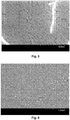
- Fig. 4 shows an SEM image of a thin layer of silver deposited on a glass substrate.
- the silver layer is 12 nm thick and was applied to the glass substrate by means of thermal evaporation. As in Fig. 4 it can be seen that the silver layer tends to form islands; the glass substrate can be seen between the metal islands. The silver layer is therefore not smooth and homogeneous on the glass substrate.
- the sheet resistance of this silver layer measured with a four-point measuring device is 19.3 ⁇ / ⁇ ⁇ 1.9 ⁇ / ⁇ .
- Fig. 5 shows a SEM image of a 12 nm silver layer, which is deposited on an organic substrate by thermal evaporation.
- the organic substrate is deposited on a glass substrate and consists of a conventional matrix material, such as, for example, ⁇ -NPD (N, N'-diphenyl-N, N'-bis (1-naphthyl) -1,1'biphenyl-4,4 "diamine
- ⁇ -NPD N, N'-diphenyl-N, N'-bis (1-naphthyl) -1,1'biphenyl-4,4 "diamine
- the tendency of the silver layer to form islands is much lower than in Fig. 4 ; however, clear cracks can be seen.
- the surface resistance of this silver layer measured with a four-point measuring device is 7.13 ⁇ / ⁇ ⁇ 0.37 ⁇ / ⁇ .
- Fig. 6 shows an SEM image of a 12 nm thick silver layer which was deposited by sputtering on a 17 nm thick ITO growth layer not according to the invention.
- This ITO growth layer was made on a 90 nm thick organic substrate, as described above, for example Fig. 5 is specified, applied.
- the organic substrate was applied to a glass substrate.
- the silver layer is as in Fig. 6 can be seen, smooth and closed.
- the surface resistance of this silver layer measured with a four-point measuring device is 4.48 ⁇ / ⁇ ⁇ 0.20 ⁇ / ⁇ .
- the thin amorphous growth layer according to the present invention advantageously enables the Metal layer - in comparison to conventional metal layers or electrode layers with a thickness of, for example, 20 nm - thin, smooth and can be deposited as a closed layer on the growth layer.
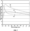
- Fig. 7 shows a graph which shows the result of a transparency measurement of the silver layers (silver layer on glass substrate according to Fig. 4 , Silver layer on organic substrate on glass substrate according to Fig. 5 and silver layer on ITO layer on organic substrate on glass substrate according to Fig. 5 ) from the 4 to 6 shows. Three measurements were carried out per example. The transparency [%] based on the wavelength [nm] is given.
- the silver layer on glass surface 19 from Fig. 4 shows a radiance of approximately 65% at a wavelength of approximately 355 nm, which drops to a minimum value of approximately 35% from approximately 410 nm and remains constant at higher wavelengths.
- the silver layer on organic background 21 Fig. 5 shows a transparency maximum of about 43% at about 400 nm. The transparency slowly drops to a value of about 32% at higher wavelengths.
- the silver layer on indium-doped tin oxide (ITO) 23 Fig. 6 shows a transparency maximum of about 68% at about 400 nm. In the range from about 380 nm to about 450 nm, the transparency is greater than 60%. The transparency of the silver layer on indium-doped tin oxide 23 is significantly greater than that of the other layers 19 and 21.
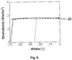
- Fig. 8 shows the radiation characteristics of an optoelectronic component. Three measurements were carried out. The radiation characteristics are shown as radiance (specified in [W / (sr / m 2 )]) in relation to the viewing angle (specified in degrees [°]). The Unit “sr” denotes the steradian, ie the solid angle.
- the Lambert radiation pattern is shown as a dashed line and has no reference number.
Description
Die vorliegende Erfindung betrifft ein elektronisches Bauelement mit einer auf einer Aufwachsschicht angeordneten, eine Metallschicht enthaltenden Elektrode.The present invention relates to an electronic component with an electrode arranged on a growth layer and containing a metal layer.
Bei großflächigen Anwendungen setzen dünne elektrische Kontakte elektronischer Bauelemente, wie beispielsweise optoelektronischer Bauelemente, insbesondere als Deckkontakte, eine gute Bestromung bzw. Leitfähigkeit und gegebenenfalls ausreichende Transparenz voraus.In large-area applications, thin electrical contacts of electronic components, such as optoelectronic components, in particular as cover contacts, require good current supply or conductivity and, if appropriate, sufficient transparency.
Die Druckschrift
In der Druckschrift
Ein transparentes, lichtemittierendes Bauelement findet sich in der Druckschrift
Aus der Druckschrift
Es offenbart die Druckschrift
In der Druckschrift
Eine Aufgabe der vorliegenden Erfindung ist, ein elektronisches Bauelement mit einer eine Metallschicht aufweisenden Elektrode mit gegenüber dem Stand der Technik verminderter Dicke und verbesserter Transparenz bereitzustellen.An object of the present invention is an electronic component with an electrode having a metal layer compared to the prior art to provide reduced thickness and improved transparency.
Die erfindungsgemäße Aufgabe wird durch ein elektronisches Bauelement mit den Merkmalen des unabhängigen Anspruchs 1 gelöst. Unteransprüche geben weitere Ausführungsformen des elektronischen Bauelements an.The object of the invention is achieved by an electronic component with the features of
Das erfindungsgemäße elektronische Bauelement weist ein Substrat, wenigstens eine auf dem Substrat angeordnete, erste Elektrode und auf der dem Substrat zugewandten Seite der Elektrode eine Aufwachsschicht auf. Die auf der Aufwachsschicht angeordnete Elektrode weist eine Metallschicht mit einer Dicke von kleiner oder gleich 30 nm auf und die Aufwachsschicht besitzt eine Dicke, die kleiner oder gleich 10 nm ist.The electronic component according to the invention has a substrate, at least one first electrode arranged on the substrate and a growth layer on the side of the electrode facing the substrate. The electrode arranged on the growth layer has a metal layer with a thickness of less than or equal to 30 nm and the growth layer has a thickness which is less than or equal to 10 nm.
Ein "Substrat", wie es hierin verwendet wird, kann zum Beispiel ein Substrat, wie es im Stand der Technik herkömmlich für ein elektronisches Bauelement verwendet wird, umfassen. Das Substrat kann ein transparentes Substrat sein. Es kann jedoch auch ein nicht transparentes Substrat sein. Beispielsweise kann das Substrat Glas, Quarz, Saphir, Kunststofffolien, Metall, Metallfolien, Siliziumwafer oder ein anderes geeignetes Substratmaterial umfassen. Ein Metallsubstrat wird im Regelfall nur dann Verwendung finden, wenn nicht direkt darauf die Aufwachsschicht angeordnet ist. Als Substrat wird erfindungsgemäß insbesondere die Schicht verstanden, auf der bei der Herstellung des elektronischen Bauelements nachfolgend alle anderen Schichten aufgebracht werden. Solche nachfolgenden Schichten können z.B. bei einem optischen elektronischen Bauelement oder einer strahlungsemittierenden Vorrichtung für die Strahlungsemission erforderliche Schichten sein.A "substrate" as used herein may include, for example, a substrate as is conventionally used in the art for an electronic device. The substrate can be a transparent substrate. However, it can also be a non-transparent substrate. For example, the substrate can comprise glass, quartz, sapphire, plastic films, metal, metal films, silicon wafers or another suitable substrate material. A metal substrate will generally only be used if the growth layer is not arranged directly on it. According to the invention, the substrate is understood in particular to be the layer on which all other layers are subsequently applied during the production of the electronic component. Such subsequent layers can e.g. in the case of an optical electronic component or a radiation-emitting device, layers required for the radiation emission.
Die "erste Elektrode" kann eine Anode oder eine Kathode sein.The "first electrode" can be an anode or a cathode.
Der Begriff "Aufwachsschicht", wie er hierin verwendet wird, bezeichnet eine Schicht, auf welcher eine eine Metallschicht umfassende Elektrode (im Folgenden auch als Aufwachselektrode bezeichnet) angeordnet ist.The term "growth layer" as used herein denotes a layer on which an electrode comprising a metal layer (also referred to below as growth electrode) is arranged.
Der Beitrag der Aufwachsschicht zur lateralen Stromleitung ist vernachlässigbar.The contribution of the growth layer to the lateral power line is negligible.
Die Aufwachsschicht ist erfindungsgemäß aus Al2O3, WO3, oder Re2O7 gebildet. Da die Aufwachsschicht eine sehr dünne Schicht ist, muss sie nicht leitfähig sein.According to the invention, the growth layer is formed from Al 2 O 3 , WO 3 , or Re 2 O 7 . Since the growth layer is a very thin layer, it does not have to be conductive.
Die Aufwachsschicht kann mittels physikalischer Gasphasenabscheidung, zum Beispiel Verdampfungsverfahren, wie thermischem Verdampfen, Elektronenstrahlverdampfen, Laserstrahlverdampfen, Lichtbogenverdampfen, Molekularstrahlepitaxie und dergleichen, Sputtern, wie ionenstrahlgestützter Deposition und dergleichen, oder Ionenplattieren, chemischer Gasphasenabscheidung, wie plasmaunterstützter chemischer Gasphasenabscheidung und dergleichen, oder Atomlagenabscheidung und dergleichen aufgebracht sein.The growth layer may be by physical vapor deposition, for example evaporation methods such as thermal evaporation, electron beam evaporation, laser beam evaporation, arc evaporation, molecular beam epitaxy and the like, sputtering such as ion beam deposition and the like, or ion plating, chemical vapor deposition such as plasma enhanced chemical and atomic deposition and the like, or the like be upset.
Die Oberfläche der Aufwachsschicht ist insbesondere in geeigneter Weise vorbereitet oder ausgelegt, um eine gleichmäßige bzw. homogene Abscheidung einer darauf abzuscheidenden Metallschicht zu ermöglichen. In einer Ausführungsform kann die Oberfläche der Aufwachsschicht eine amorphe oder im Wesentlichen amorphe Struktur bzw. eine amorphe oder im Wesentlichen amorphe Oberfläche aufweisen. Eine vollständig amorphe Struktur kann beispielsweise mittels Röntgenbeugung (XRD-Aufnahmen) bestätigt werden (es werden keine diskreten Bragg-Reflexe erhalten).The surface of the growth layer is in particular prepared or designed in a suitable manner to enable a metal layer to be deposited thereon to be deposited evenly or homogeneously. In one embodiment, the surface of the growth layer can be a have an amorphous or substantially amorphous structure or an amorphous or substantially amorphous surface. A completely amorphous structure can be confirmed, for example, by means of X-ray diffraction (XRD images) (no discrete Bragg reflections are obtained).
Der Begriff "Metallschicht", wie er hierin verwendet wird, bezeichnet eine Schicht, die im Wesentlichen oder vollständig aus Metall gebildet ist. Die Metallschicht ist direkt auf der Aufwachsschicht angeordnet. Sie kann epitaktisch auf der Aufwachsschicht aufgewachsen sein. Die Dicke der Metallschicht beträgt kleiner oder gleich 30 nm, beispielsweise zwischen 9 nm und 10 nm.The term "metal layer" as used herein refers to a layer that is formed substantially or entirely of metal. The metal layer is arranged directly on the growth layer. It can have grown epitaxially on the growth layer. The thickness of the metal layer is less than or equal to 30 nm, for example between 9 nm and 10 nm.
Die Metallschicht kann eine Dicke von kleiner oder gleich 15 nm aufweisen, insbesondere von kleiner oder gleich 12 nm.The metal layer can have a thickness of less than or equal to 15 nm, in particular less than or equal to 12 nm.
Bei Ausführungsformen der vorliegenden Erfindung, bei denen es insbesondere auf die Transparenz der Metallschicht ankommt, kann die Dicke der Metallschicht beispielsweise kleiner oder gleich 14 nm, insbesondere kleiner oder gleich 11 nm, betragen. Beispielsweise kann die Dicke einer Metallschicht, welche eine Ag-Schicht oder eine Schicht aus einer Ag-Legierung (z.B. eine Schicht aus einer Ag-Sm-Legierung) aufweist, kleiner oder gleich 14 nm, insbesondere kleiner oder gleich 11 nm, zum Beispiel zwischen etwa 9 nm und etwa 10 nm betragen.In embodiments of the present invention, in which the transparency of the metal layer is particularly important, the thickness of the metal layer can be, for example, less than or equal to 14 nm, in particular less than or equal to 11 nm. For example, the thickness of a metal layer which has an Ag layer or a layer made of an Ag alloy (for example a layer made of an Ag-Sm alloy) can be less than or equal to 14 nm, in particular less than or equal to 11 nm, for example between about 9 nm and about 10 nm.
Die Aufwachselektrode kann aus der Metallschicht bestehen oder eine oder weitere Schichten oder Funktionsschichten umfassen.The growth electrode can consist of the metal layer or comprise one or more layers or functional layers.
Die Metallschicht der Aufwachselektrode umfasst bevorzugt mindestens ein Metall, das ausgewählt ist aus der Gruppe, bestehend aus Aluminium, Barium, Indium, Silber, Gold, Magnesium, Calcium und Lithium sowie Kombinationen derselben. Die Metallschicht kann alternativ aus einem der vorstehend genannten Metalle oder einer Verbindung mit einem dieser Metalle oder aus mehreren dieser Metalle, insbesondere einer Legierung, bestehen.The metal layer of the growth electrode preferably comprises at least one metal which is selected from the group consisting of aluminum, barium, indium, silver, gold, magnesium, calcium and lithium and combinations thereof. The metal layer may alternatively be one of the above mentioned metals or a compound with one of these metals or from several of these metals, in particular an alloy.
Die Aufwachselektrode kann in transparenten und nichttransparenten elektronischen, optischen oder elektrooptischen Bauteilen eingesetzt werden. Die auf der Aufwachsschicht angeordnete Aufwachselektrode kann als Deckkontakt, Substratkontakt und/oder Zwischenkontakt eingesetzt werden.The wax-up electrode can be used in transparent and non-transparent electronic, optical or electro-optical components. The growth electrode arranged on the growth layer can be used as cover contact, substrate contact and / or intermediate contact.
Das erfindungsgemäße elektronische Bauelement ist als optoelektronisches Bauteil, nämlich als organische Leuchtdiode ausgeführt.The electronic component according to the invention is designed as an optoelectronic component, namely as an organic light-emitting diode.
Der Begriff "Schicht", wie er hierin verwendet wird, kann eine einzelne Schicht oder eine Schichtenfolge aus mehreren dünnen Schichten bezeichnen. Insbesondere können die Funktionsschichten, beispielsweise organische Funktionsschichten, aus mehreren Schichten gebildet sein. Die Metallschicht und die Aufwachsschicht sind meist einschichtig.The term "layer" as used herein can refer to a single layer or a sequence of layers of several thin layers. In particular, the functional layers, for example organic functional layers, can be formed from several layers. The metal layer and the growth layer are usually one layer.
Der Begriff "aufeinander angeordnet", wie er hierin verwendet wird, meint, dass eine Schicht unmittelbar in direktem mechanischem und/oder elektrischem Kontakt auf einer anderen Schicht angeordnet ist. Eine Schicht kann auch mittelbar auf einer anderen Schicht angeordnet sein, wobei dann weitere Schichten zwischen den angegebenen Schichten vorhanden sein können. Solche Schichten können dazu dienen, die Funktionalität und damit die Effizienz des elektronischen Bauelements weiter zu verbessern. Die Metallschicht ist im Regelfall direkt auf der Aufwachsschicht angeordnet.The term "arranged on top of one another" as used herein means that one layer is arranged directly in direct mechanical and / or electrical contact on another layer. A layer can also be arranged indirectly on another layer, in which case further layers can then be present between the specified layers. Such layers can serve to further improve the functionality and thus the efficiency of the electronic component. The metal layer is usually arranged directly on the growth layer.
Mit der in dem elektronischen Bauelement erfindungsgemäß vorgesehenen Kombination aus Aufwachsschicht und Metallschicht ist es in vorteilhafter Weise möglich, einen sehr dünnen und zugleich sehr leitfähigen Kontakt bereitzustellen, der - falls erforderlich - zusätzlich auch hochtransparent ausgebildet sein kann.With the combination of growth layer and metal layer provided according to the invention in the electronic component, it is advantageously possible to have a very thin and at the same time very conductive contact To provide, which - if necessary - can also be designed to be highly transparent.
Durch Abscheiden der Metallschicht auf der dünnen Aufwachsschicht kann die Aufwachselektrode in vorteilhafter Weise gleichmäßig, glatt und im Wesentlichen homogen ausgebildet werden. Sie kann insbesondere aus diesem Grund wesentlich dünner ausgeführt werden als nach dem Stand der Technik. Somit ist es - anders als mit den im Stand der Technik eingesetzten transparenten Kontakten aus entweder transparenten leitenden Oxiden mit einer Leitfähigkeit von größer 15 Ω/□ oder dünnen Metallschichten mit einer Dicke von mindestens 20 nm - in vorteilhafter Weise möglich, eine hohe Transparenz und gute Bestromung auch bei großflächigen Anwendungen zu erreichen.By depositing the metal layer on the thin growth layer, the growth electrode can advantageously be made uniform, smooth and essentially homogeneous. For this reason in particular, it can be made much thinner than in the prior art. In contrast to the transparent contacts made of either transparent conductive oxides with a conductivity of greater than 15 Ω / □ or thin metal layers with a thickness of at least 20 nm - in contrast to the transparent contacts used in the prior art - it is advantageously possible to have high transparency and good quality Achieve current even in large-scale applications.
Bei den erfindungsgemäßen elektronischen Bauelementen, bei denen eine Transparenz wesentlich ist, kann somit in vorteilhafter Weise ein Kompromiss zwischen Transparenz und Leitfähigkeit transparenter metallischer Kontakte eingegangen werden, da die auf der Aufwachsschicht abgeschiedene Metallschicht in vorteilhafter Weise hinreichend dünn, glatt und geschlossen gebildet sein kann, um so beispielsweise eine ausreichende Leitfähigkeit und gleichzeitig eine hervorragende Transparenz bereitzustellen.In the electronic components according to the invention, in which transparency is essential, a compromise between transparency and conductivity of transparent metallic contacts can thus advantageously be entered into, since the metal layer deposited on the growth layer can advantageously be sufficiently thin, smooth and closed, to provide sufficient conductivity and excellent transparency, for example.
Weitere Ausgestaltungen der strahlungsemittierenden Vorrichtung sind Gegenstand von Unteransprüchen.Further embodiments of the radiation-emitting device are the subject of subclaims.
In einer Weiterbildung des erfindungsgemäßen elektronischen Bauelements besitzt die Aufwachsschicht insbesondere eine Dicke von 1 nm bis 8 nm. Die Aufwachsschicht besitzt bevorzugt eine Dicke von 3 nm bis 3,5 nm. In bestimmten Ausführungsformen kann eine Dicke von größer oder gleich 1,5 nm vorteilhaft sein. Die Dicke der Aufwachsschicht kann in bestimmten Ausführungsformen beispielsweise kleiner oder gleich 7 nm sein.In a further development of the electronic component according to the invention, the growth layer has in particular a thickness of 1 nm to 8 nm. The growth layer preferably has a thickness of 3 nm to 3.5 nm. In certain embodiments, a thickness of greater than or equal to 1.5 nm can be advantageous his. The thickness of the growth layer can, for example, be less than or equal to 7 nm in certain embodiments.
In einer nicht erfindungsgemäßen Abwandlung des elektronischen Bauelements ist die Aufwachsschicht ausgewählt aus einer Schicht aus Indium-dotiertem Zinnoxid (ITO) und einer Schicht aus Aluminium-dotiertem Zinkoxid (AZO).In a modification of the electronic component not according to the invention, the growth layer is selected from a layer of indium-doped tin oxide (ITO) and a layer of aluminum-doped zinc oxide (AZO).
In einer Weiterbildung des erfindungsgemäßen elektronischen Bauelements weist die Metallschicht eine Dickenhomogenität von ± 10 % häufig sogar ± 5 %, auf. Der Begriff "Dickenhomogenität", wie er hierin verwendet wird, meint, dass die Metallschicht eine über ihre im Wesentlichen oder vollständige Länge nahezu konstante Dicke, d.h. eine Dicke mit einer maximalen Abweichung von z.B. ± 10 %, besitzen kann. Dies kann beispielsweise insbesondere durch die unter der Metallschicht angeordnete (dünne) Aufwachsschicht erreicht werden.In a development of the electronic component according to the invention, the metal layer has a thickness homogeneity of ± 10%, often even ± 5%. The term "thickness homogeneity" as used herein means that the metal layer has a thickness that is almost constant over its substantially or full length, i.e. a thickness with a maximum deviation of e.g. ± 10%. This can be achieved, for example, in particular by the (thin) growth layer arranged under the metal layer.
Die Maximaldicke einer "30 nm dicken" Metallschicht kann also beispielsweise maximal 33 nm betragen, die maximale Dicke einer "12 nm dicken" Metallschicht beispielsweise maximal 13,2 nm.The maximum thickness of a "30 nm thick" metal layer can therefore be, for example, a maximum of 33 nm, the maximum thickness of a "12 nm thick" metal layer, for example, a maximum of 13.2 nm.
In einer weiteren Ausführungsform der vorliegenden Erfindung beträgt der Flächenwiderstand der Aufwachselektrode auf der Aufwachsschicht kleiner oder gleich 6 Ω/□. Der Flächenwiderstand kann insbesondere kleiner oder gleich 5 Ω/□ betragen. Beispielsweise kann der Flächenwiderstand zwischen 4 Ω/□ und 5 Ω/□ betragen.In a further embodiment of the present invention, the surface resistance of the growth electrode on the growth layer is less than or equal to 6 Ω / □. The surface resistance can in particular be less than or equal to 5 Ω / □. For example, the surface resistance can be between 4 Ω / □ and 5 Ω / □.
Der Begriff "Flächenwiderstand", wie er hierin verwendet wird, bezeichnet den isotropen spezifischen Widerstand einer Schicht bezogen auf die Dicke derselben. Der Flächenwiderstand kann beispielsweise mit Hilfe der Vier-Punkt-Methode gemessen werden. Alternativ kann ein Flächenwiderstand auch mit der speziellen Van-der-Pauw-Methode gemessen werden.The term "sheet resistance" as used herein denotes the isotropic resistivity of a layer based on its thickness. The surface resistance can be measured using the four-point method, for example. Alternatively, a surface resistance can also be measured using the special Van der Pauw method.
Der Flächenwiderstand kann damit in vorteilhafter Weise geringer sein, als es bislang im Stand der Technik mit vergleichbaren Elektrodenschichten üblich war, die auf einem anderen Substrat als der Aufwachsschicht gemäß der vorliegenden Erfindung abgeschieden wurden. Mit der erfindungsgemäßen Anordnung kann es in vorteilhafter Weise möglich sein, eine gleichmäßige Bestromung der dünnen Aufwachselektrode - in optoelektronischen Bauelementen bei ausreichender Transparenz - zu erreichen.The surface resistance can thus advantageously be lower than has hitherto been customary in the prior art with comparable electrode layers which have been deposited on a substrate other than the growth layer according to the present invention. With the arrangement according to the invention, it can advantageously be possible to achieve a uniform energization of the thin growth electrode - in optoelectronic components with sufficient transparency.
Es ist das erfindungsgemäße elektronische Bauelement ein organisch elektronisches Bauelement und weist ferner eine zweite Elektrode und wenigstens eine zwischen der ersten Elektrode und der zweiten Elektrode angeordnete organische Funktionsschicht auf.The electronic component according to the invention is an organic electronic component and furthermore has a second electrode and at least one organic functional layer arranged between the first electrode and the second electrode.
Das organisch elektronische Bauelement ist eine strahlungsemittierende Vorrichtung.The organic electronic component is a radiation-emitting device.
Die "erste Elektrode" kann eine Anode sein. Sie kann lochinjizierende Funktionen aufweisen.The "first electrode" can be an anode. It can have hole-injecting functions.
Die "zweite Elektrode" kann eine Kathode sein.
Die erste Elektrode und die zweite Elektrode sind in geeigneter Weise elektrisch kontaktiert.The "second electrode" can be a cathode.
The first electrode and the second electrode are electrically contacted in a suitable manner.
Die Elektrode, welche auf der Aufwachsschicht angeordnet ist, wird - wie vorher angegeben - auch als Aufwachselektrode bezeichnet. Die Aufwachselektrode kann als Anode oder Kathode vorgesehen sein oder einen Teil einer solchen bilden. Der Klarheit halber wird gemäß der vorliegenden Erfindung stets von Anordnungen gesprochen, die genau eine Aufwachselektrode aufweisen. Allerdings können auch beide Elektroden eine Aufwachsschicht mit direkt darauf angeordneter Metallschicht aufweisen.The electrode, which is arranged on the growth layer, is - as previously indicated - also referred to as the growth electrode. The growth electrode can be provided as an anode or cathode or form part of one. For the sake of clarity, the present invention always refers to arrangements which have exactly one growth electrode. However, both electrodes can also have a growth layer with a metal layer arranged directly thereon.
Die Elektrode, die nicht auf einer Aufwachsschicht angeordnet ist, kann aus einem Material gebildet sein oder ein Material umfassen, das ausgewählt ist aus Metallen wie Aluminium, Barium, Indium, Silber, Gold, Magnesium, Calcium und Lithium sowie Kombinationen derselben oder einer Verbindung derselben, insbesondere einer Legierung, sowie transparenten leitfähigen Oxiden, wie beispielsweise Metalloxiden, wie Zinkoxid, Zinnoxid, Cadmiumoxid, Titanoxid, Indiumoxid oder Indium-dotiertem Zinnoxid (ITO), Aluminium-dotiertem Zinkoxid (AZO) , Zn2SnO4, CdSnO3, ZnSnO3, Mgln2O4, GaInO3, Zn2In2O5 oder In4Sn3O12 oder Mischungen unterschiedlicher transparenter leitender Oxide.The electrode, which is not arranged on a growth layer, can be formed from a material or comprise a material which is selected from metals such as aluminum, barium, indium, silver, gold, magnesium, calcium and lithium and combinations thereof or a compound thereof , in particular an alloy, and transparent conductive oxides, such as metal oxides such as zinc oxide, tin oxide, cadmium oxide, titanium oxide, indium oxide or indium-doped tin oxide (ITO), aluminum-doped zinc oxide (AZO), Zn 2 SnO 4 , CdSnO 3 , ZnSnO 3 , Mgln 2 O 4 , GaInO 3 , Zn 2 In 2 O 5 or In 4 Sn 3 O 12 or mixtures of different transparent conductive oxides.
Eine "organische Funktionsschicht" kann Emitterschichten, beispielsweise mit fluoreszierenden und/oder phosphoreszierenden Emittern, enthalten.An “organic functional layer” can contain emitter layers, for example with fluorescent and / or phosphorescent emitters.
Beispiele für Emittermaterialien, die in dem erfindungsgemäßen elektronischen Bauelement bzw. der strahlungsemittierenden Vorrichtung der vorliegenden Erfindung eingesetzt werden können, schließen organische oder organometallische Verbindungen, wie Derivate von Polyfluoren, Polythiophen und Polyphenylen (z.B. 2- oder 2,5-substituiertes Poly-p-phenylenvinylen) sowie Metallkomplexe, beispielsweise Iridium-Komplexe wie blau phosphoreszierendes FIrPic (Bis(3,5-difluoro-2-(2-pyridyl)phenyl-(2-carboxypyridyl)-iridium III), grün phosphoreszierendes Ir(ppy)3 (Tris(2-phenylpyridin)iridium III), rot phosphoreszierendes Ru (dtb-bpy)3*2(PF6) (Tris[4,4'-di-tert-butyl-(2,2')-bipyridin]ruthenium(III)komplex) sowie blau fluoreszierendes DPAVBi (4,4-Bis[4-(di-p-tolylamino)styryl]biphenyl), grün fluoreszierendes TTPA (9,10-Bis[N,N-di-(p-tolyl)-amino]anthracen) und rot fluoreszierendes DCM2 (4-Dicyanomethylen)-2-methyl-6-julolidyl-9-enyl-4H-pyran) als nichtpolymere Emitter ein. Solche nichtpolymeren Emitter sind beispielsweise mittels thermischem Verdampfen abscheidbar. Ferner können Polymeremitter eingesetzt werden, welche insbesondere mittels nasschemischen Verfahren, wie beispielsweise Spin Coating, abscheidbar sind.Examples of emitter materials which can be used in the electronic component according to the invention or the radiation-emitting device of the present invention include organic or organometallic compounds, such as derivatives of polyfluorene, polythiophene and polyphenylene (for example 2- or 2,5-substituted poly-p- phenylene vinylene) and metal complexes, for example iridium complexes such as blue phosphorescent FIrPic (bis (3,5-difluoro-2- (2-pyridyl) phenyl- (2-carboxypyridyl) iridium III), green phosphorescent Ir (ppy) 3 (Tris (2-phenylpyridine) iridium III), red phosphorescent Ru (dtb-bpy) 3 * 2 (PF 6 ) (tris [4,4'-di-tert-butyl- (2,2 ') - bipyridine] ruthenium (III ) complex) as well as blue fluorescent DPAVBi (4,4-bis [4- (di-p-tolylamino) styryl] biphenyl), green fluorescent TTPA (9,10-bis [N, N-di- (p-tolyl) - amino] anthracene) and red fluorescent DCM2 (4-dicyanomethylene) -2-methyl-6-julolidyl-9-enyl-4H-pyran) as non-polymeric emitters. Such non-polymeric emitters can be deposited, for example, by means of thermal evaporation. Can also Polymer emitters are used, which can be deposited in particular by means of wet chemical processes, such as spin coating.
Die Emittermaterialien können in geeigneter Weise in einem Matrixmaterial eingebettet sein.The emitter materials can be suitably embedded in a matrix material.
Die Emittermaterialien der Emitterschichten des elektronischen Bauelements können insbesondere so ausgewählt sein, dass das elektronische Bauelement Weißlicht emittiert. Die Emitterschicht kann mehrere verschiedenfarbig (zum Beispiel blau und gelb oder blau, grün und rot) emittierende Emittermaterialien umfassen, alternativ kann die Emitterschicht auch aus mehreren Teilschichten aufgebaut sein, wie einer blau fluoreszierenden Emitterschicht, einer grün phosphoreszierenden Emitterschicht und einer rot phosphoreszierenden Emitterschicht. Durch die Mischung der verschiedenen Farben kann die Emission von Licht mir einem weißen Farbeindruck resultieren. Alternativ kann auch vorgesehen sein, im Strahlengang der durch diese Schichten erzeugten Primäremission ein Konvertermaterial anzuordnen, das die Primärstrahlung zumindest teilweise absorbiert und eine Sekundärstrahlung anderer Wellenlänge emittiert, so dass sich aus einer (noch nicht weißen) Primärstrahlung durch die Kombination von primärer und sekundärer Strahlung ein weißer Farbeindruck ergibt.The emitter materials of the emitter layers of the electronic component can in particular be selected such that the electronic component emits white light. The emitter layer can comprise a plurality of differently colored (for example blue and yellow or blue, green and red) emitter materials, alternatively the emitter layer can also be composed of several partial layers, such as a blue fluorescent emitter layer, a green phosphorescent emitter layer and a red phosphorescent emitter layer. By mixing the different colors, the emission of light can result in a white color impression. Alternatively, it can also be provided to arrange a converter material in the beam path of the primary emission generated by these layers, which at least partially absorbs the primary radiation and emits secondary radiation of a different wavelength, so that primary radiation (not yet white) results from the combination of primary and secondary radiation a white color impression results.
Das elektronische Bauelement kann allgemein weitere organische Funktionsschichten umfassen, die dazu dienen, die Funktionalität und damit die Effizienz des elektronischen Bauelements weiter zu verbessern.The electronic component can generally comprise further organic functional layers which serve to further improve the functionality and thus the efficiency of the electronic component.
Beispielsweise können organische Funktionsschichten ausgewählt sein, die dazu dienen, die Funktionalität und die Effizienz der ersten Elektrode und/oder der zweiten Elektrode sowie des Ladungsträger- und Exzitonentransports zu verbessern.For example, organic functional layers can be selected which serve to improve the functionality and the efficiency of the first electrode and / or the second electrode as well as the charge carrier and exciton transport.
Das elektronische Bauelement kann als "Bottom-Emitter" und/oder "Top-Emitter" ausgeführt sein.The electronic component can be designed as a "bottom emitter" and / or "top emitter".
Erfindungsgemäß ist die Aufwachsschicht zwischen der organischen Funktionsschicht und Aufwachselektrode angeordnet. Die Aufwachselektrode kann dabei eine Kathode sein.According to the invention, the growth layer is arranged between the organic functional layer and the growth electrode. The growth electrode can be a cathode.
Die Anordnung der Aufwachsschicht und der Aufwachselektrode kann einen transparenten Deckkontakt für einen Top-Emitter bilden.The arrangement of the growth layer and the growth electrode can form a transparent cover contact for a top emitter.
Zusätzlich kann eine Aufwachsschicht zwischen dem Substrat und der substratseitigen Elektrode (also der Elektrode, die einen geringeren Abstand zum Substrat aufweist) als Aufwachselektrode angeordnet sein. Diese Aufwachselektrode kann dabei eine Anode sein. Das Substrat kann bevorzugt ein transparentes Substrat wie Glas, Quarz, Saphir, Kunststofffolie und dergleichen sein.In addition, a growth layer can be arranged between the substrate and the substrate-side electrode (that is, the electrode which is at a smaller distance from the substrate) as a growth electrode. This growth electrode can be an anode. The substrate can preferably be a transparent substrate such as glass, quartz, sapphire, plastic film and the like.
Die Anordnung der Aufwachsschicht und der Aufwachselektrode kann einen transparenten Substratkontakt für einen Bottom-Emitter bilden.The arrangement of the growth layer and the growth electrode can form a transparent substrate contact for a bottom emitter.
Ganz allgemein gilt, dass bei einem Top- oder Bottom-Emitter eine Elektrode der strahlungsemittierenden Vorrichtung in Form der Aufwachselektrode gemäß der vorliegenden Erfindung transparent und die andere Elektrode reflektierend ausgeführt sein kann. Alternativ dazu können auch beide Elektroden transparent ausgeführt sein.In general, it applies that, in the case of a top or bottom emitter, one electrode of the radiation-emitting device in the form of the growth electrode according to the present invention can be transparent and the other electrode can be reflective. Alternatively, both electrodes can be made transparent.
Die Metallschicht der Aufwachselektrode bildet daher insbesondere einen transparenten Dünnfilmkontakt.The metal layer of the growth electrode therefore forms, in particular, a transparent thin-film contact.
Der Begriff "Bottom-Emitter", wie er hierin verwendet wird, bezeichnet eine Ausführung, die zu der Substratseite des elektronischen Bauelements hin transparent ausgeführt ist. Insbesondere können dazu wenigstens das Substrat, die erste Elektrode und die zwischen dem Substrat und der ersten Elektrode angeordnete Aufwachsschicht transparent ausgeführt sein. Ein als Bottom-Emitter ausgeführtes elektronisches Bauelement kann demnach beispielsweise in den organischen Funktionsschichten erzeugte Strahlung auf der Substratseite des elektronischen Bauelements emittieren.The term "bottom emitter", as used herein, refers to an embodiment that faces the substrate side of the electronic component is designed to be transparent. In particular, at least the substrate, the first electrode and the growth layer arranged between the substrate and the first electrode can be made transparent. An electronic component designed as a bottom emitter can accordingly, for example, emit radiation generated in the organic functional layers on the substrate side of the electronic component.
Alternativ oder zusätzlich dazu kann das erfindungsgemäße elektronische Bauelement als "Top-Emitter" ausgeführt sein. Der Begriff "Top-Emitter", wie er hierin verwendet wird, bezeichnet eine Ausführung, die zu der Seite der zweiten Elektrode des elektronischen Bauelements hin transparent ausgeführt ist. Insbesondere können dazu die Aufwachsschicht und die Aufwachselektrode substratfern angeordnet sein und transparent ausgeführt sein. Ein als Top-Emitter ausgeführtes elektronisches Bauelement kann demnach beispielsweise in den organischen Funktionsschichten erzeugte Strahlung auf der Seite der substratfernen Elektrode des elektronischen Bauelements emittieren.Alternatively or additionally, the electronic component according to the invention can be designed as a "top emitter". The term “top emitter”, as used herein, denotes an embodiment that is transparent to the side of the second electrode of the electronic component. In particular, for this purpose the growth layer and the growth electrode can be arranged remote from the substrate and can be made transparent. An electronic component designed as a top emitter can accordingly, for example, emit radiation generated in the organic functional layers on the side of the electrode of the electronic component remote from the substrate.
Ein als Top-Emitter ausgestaltetes elektronisches Bauelement der vorliegenden Erfindung, bei welchem die Aufwachsschicht und die Metallschicht als Deckkontakt vorgesehen sind, kann in vorteilhafter Weise eine hohe Lichtauskopplung und eine sehr geringe Winkelabhängigkeit der Strahlungsdichte aufweisen. Die erfindungsgemäße strahlungsemittierende Vorrichtung kann in vorteilhafter Weise für Beleuchtungen, wie beispielsweise Raumleuchten, eingesetzt werden.An electronic component of the present invention designed as a top emitter, in which the growth layer and the metal layer are provided as cover contacts, can advantageously have a high level of light decoupling and a very low angle dependence of the radiation density. The radiation-emitting device according to the invention can be used advantageously for lighting, such as room lights.
Eine Kombination aus Bottom- und Top-Emitter ist in gleicher Weise möglich. Bei einer solchen Ausführung ist das elektronische Bauelement allgemein in der Lage, das in den organischen Funktionsschichten erzeugte Licht in beide Richtungen - also sowohl zu der Substratseite als auch zu der substratfernen Seite hin - zu emittieren.A combination of bottom and top emitter is possible in the same way. In such an embodiment, the electronic component is generally capable of emitting the light generated in the organic functional layers in both directions - that is, both towards the substrate side and towards the side remote from the substrate.
In einer weiteren Ausführungsform der vorliegenden Erfindung ist zwischen der ersten Elektrode und der zweiten Elektrode wenigstens eine dritte Elektrode angeordnet.In a further embodiment of the present invention, at least one third electrode is arranged between the first electrode and the second electrode.
Die "dritte Elektrode" kann als Zwischenkontakt fungieren. Sie kann dazu dienen, einen Ladungstransport durch die Schichten des elektronischen Bauelements hindurch zu erhöhen und damit die Effizienz des elektronischen Bauelements in vorteilhafter Weise zu verbessern. Die dritte Elektrode kann als ambipolare Schicht ausgestaltet sein; sie kann als Kathode oder Anode ausgestaltet sein. Die Anordnung der Aufwachsschicht und der Aufwachselektrode der vorliegenden Ausführungsform bildet dann einen transparenten Zwischenkontakt. Ebenso wie die erste und die zweite Elektrode ist die dritte Elektrode elektrisch kontaktiert.The "third electrode" can act as an intermediate contact. It can be used to increase charge transport through the layers of the electronic component and thus to improve the efficiency of the electronic component in an advantageous manner. The third electrode can be designed as an ambipolar layer; it can be configured as a cathode or anode. The arrangement of the growth layer and the growth electrode of the present embodiment then forms a transparent intermediate contact. Like the first and second electrodes, the third electrode is electrically contacted.
In einer Weiterbildung des elektronischen Bauelements der vorliegenden Erfindung sind als organische Funktionsschichten eine Emitterschicht und eine oder mehrere weitere organische Funktionsschichten enthalten. Die weiteren organischen Funktionsschichten können ausgewählt sein aus der Gruppe, bestehend aus Lochinjektionsschichten, Lochtransportschichten, lochblockierenden Schichten, Elektroneninjektionsschichten, Elektronentransportschichten und elektronenblockierenden Schichten.In a further development of the electronic component of the present invention, an organic layer and an emitter layer and one or more further organic functional layers are included. The further organic functional layers can be selected from the group consisting of hole injection layers, hole transport layers, hole blocking layers, electron injection layers, electron transport layers and electron blocking layers.
Geeignete Funktionsschichten und geeignete organische Funktionsschichten sind dem Fachmann bekannt. Die (organischen) Funktionsschichten können vorzugsweise mittels thermischem Verdampfen aufgebracht werden. Die weiteren (organischen) Funktionsschichten können die Funktionalität und/oder Effizienz des elektronischen Bauelements in vorteilhafter Weise verbessern.Suitable functional layers and suitable organic functional layers are known to the person skilled in the art. The (organic) functional layers can preferably be applied by means of thermal evaporation. The further (organic) functional layers can advantageously improve the functionality and / or efficiency of the electronic component.
In einer weiteren Ausführungsform der vorliegenden Erfindung ist das elektronische Bauelement als organische Leuchtdiode (OLED) ausgebildet.In a further embodiment of the present invention, the electronic component is designed as an organic light-emitting diode (OLED).
In einer Weiterbildung des elektronischen Bauelements weist das elektronische Bauelement eine im Wesentlichen Lambertsche Abstrahlcharakteristik auf.In a further development of the electronic component, the electronic component has an essentially Lambertian radiation characteristic.
Der Begriff "Lambertsche Abstrahlcharakteristik", wie er hierin verwendet wird, bezeichnet das ideale Abstrahlverhalten eines so genannten Lambert-Strahlers.The term "Lambertian radiation characteristic" as used herein denotes the ideal radiation behavior of a so-called Lambert radiator.
Eine "im Wesentlichen" Lambertsche Abstrahlcharakteristik, wie sie hierin bezeichnet ist, meint dabei insbesondere, dass die Abstrahlcharakteristik, welche sich nach der Formel ![]()
![]()
Auf diese Weise kann es vorteilhaft möglich sein, eine nach allen Richtungen konstante Strahldichte bzw. Leuchtdichte des elektronischen Bauelements der vorliegenden Erfindung zu erreichen, so dass das elektronische Bauelement in allen Richtungen gleich hell scheint. Die Helligkeit des elektronischen Bauelements kann sich in vorteilhafter Weise auch dann nicht ändern, wenn es gegenüber der Blickrichtung verkippt wird.In this way it can advantageously be possible to achieve a radiance or luminance of the electronic component of the present invention that is constant in all directions, so that the electronic component appears equally bright in all directions. The brightness of the electronic component can advantageously not change even if it is tilted relative to the viewing direction.
In einer weiteren Ausführungsform beträgt die Transparenz des elektronischen Bauelements größer oder gleich 60 %.In a further embodiment, the transparency of the electronic component is greater than or equal to 60%.
Vorzugsweise kann die Transparenz größer oder gleich 65 % betragen. Die Transparenz wird mittels Intensitätsmessungen gemessen, indem vorgegebene Wellenlängenbereich abgetastet und die durch die strahlungsemittierende Vorrichtung tretende Lichtmenge erfasst wird.The transparency can preferably be greater than or equal to 65%. The transparency is measured by means of intensity measurements, by scanning the predetermined wavelength range and detecting the amount of light passing through the radiation-emitting device.
Der Begriff "Transparenz", wie er hierin verwendet wird, bezeichnet die Fähigkeit der einzelnen Schichten des erfindungsgemäßen elektronischen Bauelements, elektromagnetische Wellen - und insbesondere sichtbares Licht - durchzulassen. Die Transparenz des elektronischen Bauelements gemäß der vorliegenden Erfindung beträgt im Regelfall zumindest für wenigstens eine konkrete Wellenlänge mehr als 60 %, vorzugsweise mehr als 65 %. Insbesondere kann die Transparenz für wenigstens eine Wellenlänge in einem Wellenlängenbereich von etwa 400 nm bis etwa 450 nm mehr als 60 % und vorzugsweise mehr als 65 % betragen.The term "transparency" as used herein denotes the ability of the individual layers of the electronic component according to the invention to transmit electromagnetic waves - and in particular visible light. The transparency of the electronic component according to the present invention is generally more than 60%, preferably more than 65%, at least for at least one specific wavelength. In particular, the transparency for at least one wavelength in a wavelength range from approximately 400 nm to approximately 450 nm can be more than 60% and preferably more than 65%.
Die erfindungsgemäße Anordnung der Aufwachsschicht und der Aufwachselektrode kann somit in vorteilhafter Weise eine gegenüber dem Stand der Technik verbesserte Transparenz bei gleichzeitig ausreichender Bestromung bereitstellen.The arrangement according to the invention of the growth layer and the growth electrode can thus advantageously provide an improved transparency compared to the prior art, while at the same time providing sufficient current.
In einer weiteren Ausführungsform der vorliegenden Erfindung ist die Aufwachsschicht mittels Sputtern aufgebracht. Die Aufwachsschicht kann insbesondere mittels Facing Target Sputtern oder Hohlkathoden-Sputtern aufgebracht sein.In a further embodiment of the present invention, the growth layer is applied by means of sputtering. The growth layer can be applied in particular by means of facing target sputtering or hollow cathode sputtering.
Der Begriff "Facing Target Sputtern", wie er hierin verwendet wird, bezeichnet einen einstufigen Prozess, mittels dem geschlossene epitaktische Schichten erhalten werden können.The term "facing target sputtering" as used herein denotes a one-step process by means of which closed epitaxial layers can be obtained.
Der Begriff "Hohlkathoden-Sputtern", wie er hierin verwendet wird, bezeichnet ein Sputterverfahren unter Verwenden einer Hohlkathoden-Sputteranlage, welche eine Hohlkathode aus Targetmaterial aufweist. Im Vergleich zu den üblicherweise bei einem Druck von < 1 Pa ablaufenden Sputterverfahren, können beim Hohlkathoden-Sputtern verbesserte Eigenschaften der Aufwachsschicht erhalten werden, da in vorteilhafter Weise praktisch kein Bombardement der Schicht mit energetischen, vom Target reflektierten Neutralteilchen stattfindet.The term "hollow cathode sputtering" as used herein denotes a sputtering method using a hollow cathode sputtering system which has a hollow cathode made of target material. Compared to the sputtering processes that usually take place at a pressure of <1 Pa, With hollow cathode sputtering, improved properties of the growth layer can be obtained, since advantageously there is practically no bombardment of the layer with energetic neutral particles reflected from the target.
Die mittels Facing Target Sputtern oder Hohlkathoden-Sputtern abgeschiedene Aufwachsschicht weist im Regelfall ein im Wesentlichen amorphes Erscheinungsbild bzw. eine im Wesentlichen amorphe Oberfläche auf. Auf einer solchen amorphen Oberfläche kann besonders gut eine dünne Metallschicht abgeschieden werden, um auf diese Weise in vorteilhafter Weise einen transparenten Kontakt für ein elektronisches Bauelement der vorliegenden Erfindung bereitzustellen. Mittels Sputtern aufgebrachte Schichten weisen im Regelfall Einschlüsse auf, in denen das zum Sputtern verwendete Prozessgas enthalten ist (z.B. Argon).The growth layer deposited by means of facing target sputtering or hollow cathode sputtering generally has an essentially amorphous appearance or an essentially amorphous surface. A thin metal layer can be deposited particularly well on such an amorphous surface in order in this way to advantageously provide a transparent contact for an electronic component of the present invention. Layers applied by sputtering generally contain inclusions that contain the process gas used for sputtering (e.g. argon).
Durch Verwenden eines Sputterverfahrens zum Aufbringen der Aufwachsschicht kann in vorteilhafter Weise ein Abscheiden nichtstöchiometrischer Schichten, die aus einem thermischen Verdampfen bei zu hohen Temperaturen resultieren können, vermieden werden, wobei die bei reaktivem Sputtern häufig mit zunehmender Beschichtungszeit auftretenden Schädigungen der unterliegenden Schichten durch verschiedene Einflüsse aus dem Sputterplasma aufgrund der erfindungsgemäß vorgesehenen sehr dünnen Aufwachsschicht vermieden werden können.
Durch Aufbringen der Aufwachsschicht mittels Sputtern kann somit in vorteilhafter Weise ein schädigungsfreies und/oder stöchiometrisches Aufbringen der Aufwachsschicht erreicht werden. Dies kann insbesondere beispielsweise bei der Beschichtung empfindlicher Strukturen, wie sie zum Beispiel bei organischen Leuchtdioden vorhanden sind, von Vorteil sein.By using a sputtering process for applying the growth layer, deposition of non-stoichiometric layers, which can result from thermal evaporation at too high temperatures, can advantageously be avoided, the damage to the underlying layers which often occurs in reactive sputtering with increasing coating time being caused by various influences the sputtering plasma can be avoided due to the very thin growth layer provided according to the invention.
By applying the growth layer by means of sputtering, damage-free and / or stoichiometric application of the growth layer can thus be achieved in an advantageous manner. This can be particularly advantageous, for example, when coating sensitive structures, such as are present in organic light emitting diodes.
In einer weiteren Ausführungsform der vorliegenden Erfindung ist die Metallschicht zeitlich unmittelbar nach der Aufwachsschicht aufgebracht.In a further embodiment of the present invention, the metal layer is applied immediately after the growth layer.
Der Begriff "zeitlich unmittelbar aufgebracht" oder bevorzugt "hintereinander aufgebracht", wie er hierin verwendet wird, meint, dass die Metallschicht während des Herstellungsprozesses des elektronischen Bauelements zeitlich direkt nach der Aufwachsschicht abgeschieden wird, z.B. ohne Reaktorwechsel oder nicht später als einen Tag nach Abscheiden der Aufwachsschicht.The term "applied immediately in time" or preferably "applied in succession" as used herein means that the metal layer is deposited in time directly after the growth layer during the manufacturing process of the electronic component, e.g. without changing the reactor or no later than one day after the growth layer has been deposited.
Durch die unmittelbare Abscheidung der Metallschicht auf der Aufwachsschicht kann einem Altern der Aufwachsschicht vorgebeugt werden, insbesondere tritt keine oder eine nur geringe Alterung der z.B. amorphen Oberfläche ein, wodurch ihr amorphes Erscheinungsbild zum geeigneten Abscheiden der Metallschicht beibehalten werden kann.The immediate deposition of the metal layer on the growth layer can prevent aging of the growth layer, in particular there is no or only a slight aging of the e.g. amorphous surface, whereby their amorphous appearance can be retained for the appropriate deposition of the metal layer.
Das elektronische Bauelement gemäß der vorliegenden Erfindung umfasst zumindest eine weitere Funktionsschicht, gewählt aus der Gruppe von Antireflektionsschichten, Streuschichten, Schichten zur Farbkonversion von Licht und/oder mechanische Schutzschichten. Derartige Schichten werden auf der Metallschicht der Aufwachselektrode angeordnet.The electronic component according to the present invention comprises at least one further functional layer, selected from the group of antireflection layers, scattering layers, layers for color conversion of light and / or mechanical protective layers. Such layers are arranged on the metal layer of the growth electrode.
Die Funktionsschichten können vorzugsweise mittels thermischem Verdampfen abgeschieden werden. Diese Schichten können die Funktion und Effizienz der strahlungsemittierenden Vorrichtung weiter verbessern.The functional layers can preferably be deposited by means of thermal evaporation. These layers can further improve the function and efficiency of the radiation-emitting device.
Ein elektrischer Kontakt ist zur Verwendung in bzw. mit einem elektronischen Bauelement geeignet.An electrical contact is suitable for use in or with an electronic component.
Der elektrische Kontakt weist ein Substrat, wenigstens eine auf dem Substrat angeordnete, erste Elektrode und auf der dem Substrat zugewandten Seite der Elektrode eine Aufwachsschicht auf, wobei die auf der Aufwachsschicht angeordnete Elektrode eine Metallschicht mit einer Dicke von kleiner oder gleich 30 nm aufweist und die Aufwachsschicht eine Dicke besitzt, die kleiner oder gleich 10 nm ist, wobei die Aufwachsschicht insbesondere direkt auf dem Substrat angeordnet ist.The electrical contact has a substrate, at least one first electrode arranged on the substrate and a growth layer on the side of the electrode facing the substrate , wherein the electrode arranged on the growth layer has a metal layer with a thickness of less than or equal to 30 nm and the growth layer has a thickness which is less than or equal to 10 nm, the growth layer in particular being arranged directly on the substrate.
Da bereits mit dem elektrischen Kontakt im Wesentlichen alle Vorteile erzielbar sind, welche mit dem erfindungsgemäßen elektronischen Bauteil erzielt werden können, wird bezüglich weiterer Ausgestaltungen zur Vermeidung von Wiederholungen auf die vorstehenden Ausführungen hierzu verwiesen.Since essentially all of the advantages that can be achieved with the electronic component according to the invention can already be achieved with the electrical contact, reference is made to the above explanations in this regard with regard to further configurations in order to avoid repetitions.
Die vorliegende Erfindung wird im Folgenden anhand von Ausführungsformen unter Bezugnahme auf die beigefügten Figuren beschrieben. In den Figuren bezeichnen gleiche Bezugszeichen gleiche oder identische Elemente. Es zeigt:
- Fig. 1
- eine schematisch vereinfachte Seitenansicht eines elektronischen Bauelements gemäß einer Ausführungsform der vorliegenden Erfindung in einem Teilschnitt;
- Fig. 2
- eine schematisch vereinfachte Seitenansicht eines elektronischen Bauelements gemäß einer nicht erfindungsgemäßer Abwandlung in einem Teilschnitt;
- Fig. 3
- eine schematisch vereinfachte Seitenansicht eines elektronischen Bauelements gemäß einer Ausführungsform der vorliegenden Erfindung in einem Teilschnitt;
- Fig. 4
- eine REM-Aufnahme einer dünnen Silberschicht, die auf einem Glassubstrat abgeschieden ist;
- Fig. 5
- eine REM-Aufnahme einer dünnen Silberschicht, die auf einem herkömmlichen Organikuntergrund abgeschieden ist;
- Fig. 6
- eine REM-Aufnahme einer dünnen Silberschicht, die auf einer ITO-Aufwachsschicht abgeschieden ist;
- Fig. 7
- einen Graphen, der das Ergebnis einer Transparenzmessung der Silberschichten aus den
Fig. 3 zeigt; undbis 5 - Fig. 8
- Abstrahlcharakteristiken eines elektrooptischen Bauelements zeigt.
- Fig. 1
- a schematically simplified side view of an electronic component according to an embodiment of the present invention in a partial section;
- Fig. 2
- a schematically simplified side view of an electronic component according to a modification according to the invention in a partial section;
- Fig. 3
- a schematically simplified side view of an electronic component according to an embodiment of the present invention in a partial section;
- Fig. 4
- an SEM photograph of a thin layer of silver deposited on a glass substrate;
- Fig. 5
- an SEM image of a thin layer of silver deposited on a conventional organic substrate;
- Fig. 6
- an SEM image of a thin layer of silver deposited on an ITO growth layer;
- Fig. 7
- a graph which shows the result of a transparency measurement of the silver layers from the
3 to 5 shows; and - Fig. 8
- Shows radiation characteristics of an electro-optical component.
In den nachfolgenden Ausführungsformen, die anhand der Zeichnung beispielhaft beschrieben sind, ist das erfindungsgemäße elektronische Bauelement als strahlungsemittierende Vorrichtung, insbesondere als OLED, veranschaulicht.In the following embodiments, which are described by way of example with reference to the drawing, the electronic component according to the invention is illustrated as a radiation-emitting device, in particular as an OLED.
Auf einem Substrat 1, z.B. einem Glassubstrat, ist eine zweite Elektrode 11 angeordnet. Die zweite Elektrode 11 kann z.B. eine Anode sein und beispielsweise aus Indium-dotiertem Zinnoxid (ITO) gebildet sein.On a
Auf der zweiten Elektrode 11 ist eine organische Funktionsschicht 5, wie beispielsweise eine fluoreszierende und/oder phosphoreszierende Emitterschicht, angeordnet.An organic
Auf der organischen Funktionsschicht 5 ist eine Aufwachsschicht 7 angeordnet. Die Aufwachsschicht 7 kann z.B. 3 nm dick sein und mittels Facing Target Sputtern abgeschieden sein.A
Auf der Aufwachsschicht 7 ist als erste Elektrode 3 eine Aufwachselektrode, z.B. in Form einer 10 nm dicken Metallschicht 9, abgeschieden. Die Metallschicht 9 kann beispielsweise mittels Sputtern abgeschieden sein.On the
Die die Metallschicht 9 umfassende erste Elektrode 3 ist, wenn die zweite Elektrode 11 eine Anode ist, eine Kathode. Die Aufwachsschicht 7 ist dabei erfindungsgemäß auf der dem Substrat 1 zugewandten Seite der ersten Elektrode 3 angeordnet.When the
Auf dem Substrat 1, wie einem Glassubstrat, ist eine Aufwachsschicht 7 und auf der Aufwachsschicht 7 eine Aufwachselektrode in Form einer Metallschicht 9 als erste Elektrode 3 angeordnet sind. Die erste Elektrode 3 kann als Anode ausgestaltet sein. Die Aufwachsschicht 7 ist auf der dem Substrat 1 zugewandten Seite der ersten Elektrode 3 angeordnet.A
Die Aufwachsschicht 7 kann in vorteilhafter Weise dazu dienen, die Oberfläche auf der eine Aufwachselektrode aufgebracht worden ist, zu verbessern, d.h. in einer solchen Weise zu behandeln, dass die Metallschicht 9 dünn, glatt und homogen abgeschieden werden kann, um eine verbesserte Bestromung und eine verbesserte Transparenz des elektronischen Bauelements 100 zu ermöglichen.The
Auf der Metallschicht 9 ist eine organische Funktionsschicht 5 angeordnet. Die organische Funktionsschicht 5 kann eine Emitterschicht umfassen.An organic
Auf der organischen Funktionsschicht 5 ist die zweite Elektrode 11 angeordnet. Die zweite Elektrode 11 ist, wenn die erste Elektrode 3 eine Anode ist, eine Kathode. Sie kann zum Beispiel eine herkömmliche 20 nm dicke Silberschicht sein.The
Auf einem Substrat 1 ist eine zweite Elektrode 11 angeordnet. Die zweite Elektrode 11 kann, wie in
Auf der zweiten Elektrode 11 ist eine Lochinjektionsschicht 13 und auf dieser eine Lochtransportschicht 15 angeordnet. Die Lochinjektionsschicht 13 und die Lochtrabsportschicht 15 können mittels thermischem Verdampfen abgeschieden sein.A
Auf der Lochtransportschicht 15 ist eine weitere organische Funktionsschicht 5, wie beispielsweise eine fluoreszierende und/oder phosphoreszierende Emitterschicht, angeordnet.A further organic
Auf der organischen Funktionsschicht 5 ist eine Elektronentransportschicht 17 angeordnet, welche ebenfalls mittels thermischem Verdampfen abgeschieden sein kann. Auf der Elektronentransportschicht 17 ist eine Aufwachsschicht 7 angeordnet. Die Aufwachsschicht 7 kann z.B. 3 nm dick sein und mittels Facing Target Sputtern abgeschieden sein.An
Auf der Aufwachsschicht 7 ist als erste Elektrode 3 eine Aufwachselektrode, z.B. in Form einer 10 nm dicken Metallschicht 9, abgeschieden. Die Metallschicht 9 kann bevorzugt mittels Sputtern abgeschieden sein.
Die die Metallschicht 9 umfassende erste Elektrode 3 ist, wie in
The
Die dünne amorphe Aufwachsschicht gemäß der vorliegenden Erfindung ermöglicht in vorteilhafter Weise, dass die Metallschicht - im Vergleich zu herkömmlichen Metallschichten bzw. Elektrodenschichten mit einer Dicke von z.B. 20 nm - dünn, glatt und als geschlossene Schicht auf der Aufwachschicht abscheidbar ist.The thin amorphous growth layer according to the present invention advantageously enables the Metal layer - in comparison to conventional metal layers or electrode layers with a thickness of, for example, 20 nm - thin, smooth and can be deposited as a closed layer on the growth layer.
Die Silberschicht auf Glasuntergrund 19 aus
Die Silberschicht auf Organikuntergrund 21 aus
Die Silberschicht auf Indium-dotiertem Zinnoxid (ITO) 23 aus
Die Abstrahlcharakteristik 25 der in
Claims (10)
- Electronic component, comprising:- a substrate (1),- at least one first electrode (3) arranged on the substrate (1),- a growth layer (7) on the side of the electrode (3) facing the substrate (1),
wherein- the electrode (3) arranged on the growth layer (7) has a metal layer (9) with a thickness of less than or equal to 30 nm and the growth layer (7) has a thickness which is less than or equal to 10 nm,- the electronic component is formed as an organic light-emitting diode and further has a second electrode (11) and at least one organic functional layer (5, 13, 15, 17) arranged between the first electrode (3) and the second electrode (11), and- the growth layer (7) directly follows the organic functional layer (5, 13, 15, 17) in direction away from the substrate (1) and the first electrode (3) directly follows the growth layer (7) and a functional layer, which is an anti-reflection layer, a scatter layer, a layer for colour conversion of light and/or a mechanical protective layer, directly follows the first electrode (3),
characterized in that
the growth layer (7) is formed from Al2O3, WO3 or Re2O7. - Electronic component according to claim 1, wherein the growth layer (7) has a thickness of 1 nm to 8 nm.
- Electronic component according to one of the preceding claims, wherein the metal layer (9) has a thickness homogeneity of ± 10%.
- Electronic component according to one of the preceding claims, wherein the metal layer (9) comprises at least one metal selected from the group consisting of aluminum, barium, indium, silver, gold, magnesium, calcium and lithium and combinations thereof or of the metal or a compound of the metal or a plurality of the metals.
- Electronic component according to one of the preceding claims, wherein the surface resistivity of the electronic component (100) is less than or equal to 8Ω/□.
- Electronic component according to one of the preceding claims, wherein the first electrode (3) consists of the metal layer (9).
- Electronic component according to one of the preceding claims, which has a Lambertian radiation characteristic (19).
- Electronic component according to one of the preceding claims, with a transparency greater than or equal to 60 %.
- Electronic component according to one of the preceding claims, wherein the growth layer (7) is applied by means of sputtering.
- Electronic component according to one of the preceding claims, wherein the growth layer (7) has an amorphous structure.
Applications Claiming Priority (2)
| Application Number | Priority Date | Filing Date | Title |
|---|---|---|---|
| DE102009034822A DE102009034822A1 (en) | 2009-07-27 | 2009-07-27 | Electronic component as well as electrical contact |
| PCT/EP2010/060250 WO2011012461A1 (en) | 2009-07-27 | 2010-07-15 | Electronic component and electrical contact |
Publications (2)
| Publication Number | Publication Date |
|---|---|
| EP2460204A1 EP2460204A1 (en) | 2012-06-06 |
| EP2460204B1 true EP2460204B1 (en) | 2020-01-22 |
Family
ID=42957993
Family Applications (1)
| Application Number | Title | Priority Date | Filing Date |
|---|---|---|---|
| EP10732974.0A Active EP2460204B1 (en) | 2009-07-27 | 2010-07-15 | Electronic component |
Country Status (7)
| Country | Link |
|---|---|
| US (1) | US9059423B2 (en) |
| EP (1) | EP2460204B1 (en) |
| JP (1) | JP2013500559A (en) |
| KR (1) | KR101791548B1 (en) |
| CN (1) | CN102473860B (en) |
| DE (1) | DE102009034822A1 (en) |
| WO (1) | WO2011012461A1 (en) |
Families Citing this family (8)
| Publication number | Priority date | Publication date | Assignee | Title |
|---|---|---|---|---|
| DE102010040839B4 (en) * | 2010-09-15 | 2013-10-17 | Osram Opto Semiconductors Gmbh | Method for producing an electronic component and electronic component |
| DE102011108089B4 (en) * | 2011-07-18 | 2015-11-12 | Technische Universität Dresden | Process for the preparation of thin electrically conductive layers of silver, a silver complex, its solution and a use of the silver complex in a solution |
| DE102012105860A1 (en) * | 2012-07-02 | 2015-03-26 | Heliatek Gmbh | Photoactive organic device with an optically transparent electrode and method for manufacturing |
| DE102012211869A1 (en) | 2012-07-06 | 2014-01-09 | Osram Opto Semiconductors Gmbh | Organic light emitting device |
| TWI662223B (en) * | 2012-12-07 | 2019-06-11 | 樂金顯示科技股份有限公司 | Lighting apparatus |
| DE102013109646B4 (en) | 2013-09-04 | 2021-12-02 | Pictiva Displays International Limited | Organic optoelectronic component |
| US9133545B2 (en) * | 2013-10-23 | 2015-09-15 | Corning Incorporated | Glass-ceramics substrates for graphene growth |
| WO2018037880A1 (en) * | 2016-08-25 | 2018-03-01 | コニカミノルタ株式会社 | Transparent electrode and electronic device |
Citations (3)
| Publication number | Priority date | Publication date | Assignee | Title |
|---|---|---|---|---|
| JP2003288993A (en) * | 2002-03-27 | 2003-10-10 | Tokai Rubber Ind Ltd | Transparent electrode for organic electroluminescent element and organic electroluminescent element using the same |
| EP1939954A2 (en) * | 2006-12-28 | 2008-07-02 | Samsung SDI Co., Ltd. | Organic light emitting diode display device and method of fabricating the same |
| EP2012375A2 (en) * | 2007-07-03 | 2009-01-07 | Samsung SDI Co., Ltd. | Organic light emitting device |
Family Cites Families (24)
| Publication number | Priority date | Publication date | Assignee | Title |
|---|---|---|---|---|
| JP2001266654A (en) * | 2000-01-11 | 2001-09-28 | Sanyo Electric Co Ltd | Transparent electrode and its patterning method and method of manufacturing semiconductor element using the same |
| JP4556282B2 (en) * | 2000-03-31 | 2010-10-06 | 株式会社デンソー | Organic EL device and method for manufacturing the same |
| US6888305B2 (en) * | 2001-11-06 | 2005-05-03 | Universal Display Corporation | Encapsulation structure that acts as a multilayer mirror |
| JP2003303685A (en) | 2002-04-09 | 2003-10-24 | Canon Inc | Organic luminous element |
| JP2004079422A (en) | 2002-08-21 | 2004-03-11 | Tdk Corp | Organic el element |
| KR100662297B1 (en) * | 2002-10-18 | 2007-01-02 | 엘지전자 주식회사 | Organic electroluminescence device |
| US7015639B2 (en) * | 2002-10-22 | 2006-03-21 | Osram Opto Semiconductors Gmbh | Electroluminescent devices and method of making transparent cathodes |
| JP2004165068A (en) * | 2002-11-14 | 2004-06-10 | Sanyo Electric Co Ltd | Manufacturing method of organic electroluminescent panel |
| US20040140758A1 (en) * | 2003-01-17 | 2004-07-22 | Eastman Kodak Company | Organic light emitting device (OLED) display with improved light emission using a metallic anode |
| EP1615472A1 (en) | 2003-03-25 | 2006-01-11 | Kyoto University | Light-emitting device and organic electroluminescence light-emitting device |
| JP4822243B2 (en) * | 2003-03-25 | 2011-11-24 | 国立大学法人京都大学 | LIGHT EMITTING ELEMENT AND ORGANIC ELECTROLUMINESCENT LIGHT EMITTING ELEMENT |
| JP4689176B2 (en) * | 2004-02-26 | 2011-05-25 | 大日本印刷株式会社 | Organic electroluminescence device |
| US7242703B2 (en) * | 2004-12-21 | 2007-07-10 | The Trustees Of Princeton University | Organic injection laser |
| JP2006193363A (en) | 2005-01-12 | 2006-07-27 | Sumitomo Metal Mining Co Ltd | Oxide sintered compact, sputtering target, and transparent electroconductive thin film |
| EP1701395B1 (en) | 2005-03-11 | 2012-09-12 | Novaled AG | Transparent light emitting element |
| JP2006337447A (en) * | 2005-05-31 | 2006-12-14 | Victor Co Of Japan Ltd | Manufacturing method of liquid crystal display element, and the liquid crystal display element |
| JP2007013049A (en) * | 2005-07-04 | 2007-01-18 | Sharp Corp | Flexible circuit and electronic apparatus utilizing the same |
| JP2007165284A (en) | 2005-11-18 | 2007-06-28 | Seiko Instruments Inc | Electroluminescent device and display using same |
| KR100845694B1 (en) | 2006-01-18 | 2008-07-11 | 주식회사 엘지화학 | Oled having stacked organic light-emitting units |
| WO2008001241A2 (en) * | 2006-06-14 | 2008-01-03 | Philips Intellectual Property & Standards Gmbh | Structured oled with micro optics for generating directed light |
| JP5109303B2 (en) | 2006-07-31 | 2012-12-26 | ソニー株式会社 | Organic light emitting device and display device |
| US20080105299A1 (en) * | 2006-11-02 | 2008-05-08 | Guardian Industries Corp. | Front electrode with thin metal film layer and high work-function buffer layer for use in photovoltaic device and method of making same |
| FR2925981B1 (en) * | 2007-12-27 | 2010-02-19 | Saint Gobain | CARRIER SUBSTRATE OF AN ELECTRODE, ORGANIC ELECTROLUMINESCENT DEVICE INCORPORATING IT. |
| TWI420722B (en) * | 2008-01-30 | 2013-12-21 | Osram Opto Semiconductors Gmbh | Device with encapsulation unit |
-
2009
- 2009-07-27 DE DE102009034822A patent/DE102009034822A1/en not_active Withdrawn
-
2010
- 2010-07-15 CN CN201080033615.4A patent/CN102473860B/en active Active
- 2010-07-15 WO PCT/EP2010/060250 patent/WO2011012461A1/en active Application Filing
- 2010-07-15 KR KR1020127004650A patent/KR101791548B1/en active IP Right Grant
- 2010-07-15 US US13/387,690 patent/US9059423B2/en active Active
- 2010-07-15 JP JP2012522092A patent/JP2013500559A/en active Pending
- 2010-07-15 EP EP10732974.0A patent/EP2460204B1/en active Active
Patent Citations (3)
| Publication number | Priority date | Publication date | Assignee | Title |
|---|---|---|---|---|
| JP2003288993A (en) * | 2002-03-27 | 2003-10-10 | Tokai Rubber Ind Ltd | Transparent electrode for organic electroluminescent element and organic electroluminescent element using the same |
| EP1939954A2 (en) * | 2006-12-28 | 2008-07-02 | Samsung SDI Co., Ltd. | Organic light emitting diode display device and method of fabricating the same |
| EP2012375A2 (en) * | 2007-07-03 | 2009-01-07 | Samsung SDI Co., Ltd. | Organic light emitting device |
Also Published As
| Publication number | Publication date |
|---|---|
| JP2013500559A (en) | 2013-01-07 |
| KR101791548B1 (en) | 2017-10-30 |
| EP2460204A1 (en) | 2012-06-06 |
| US20120175668A1 (en) | 2012-07-12 |
| DE102009034822A1 (en) | 2011-02-03 |
| CN102473860A (en) | 2012-05-23 |
| WO2011012461A1 (en) | 2011-02-03 |
| US9059423B2 (en) | 2015-06-16 |
| CN102473860B (en) | 2015-09-30 |
| KR20120052345A (en) | 2012-05-23 |
Similar Documents
| Publication | Publication Date | Title |
|---|---|---|
| EP2460204B1 (en) | Electronic component | |
| DE102010040839B4 (en) | Method for producing an electronic component and electronic component | |
| EP2321863B1 (en) | Method for producing an organic radiation-emitting component and organic radiation-emitting component | |
| DE102008020816B4 (en) | Organic light-emitting diode, planar, optically active element with a contact arrangement and method for producing an organic light-emitting diode | |
| DE102011054774B4 (en) | WHITE LIGHT EMITTING ORGANIC DEVICES | |
| DE102013109451B9 (en) | Method for producing an optoelectronic component | |
| DE102007024152A1 (en) | Organic optoelectronic component | |
| DE112009001283T5 (en) | Organic electroluminescent element | |
| EP2529604B1 (en) | Light source on a printed circuit board and arrangement of light sources | |
| WO2008061524A2 (en) | Lighting element, and method for the production thereof | |
| DE112018004850T5 (en) | TRANSPARENT LADDER AND ORGANIC DEVICE | |
| DE102008049057A1 (en) | Organic opto-electrical component and a method for producing an organic opto-electrical component | |
| DE102013109646B4 (en) | Organic optoelectronic component | |
| DE102013114455B4 (en) | Organic light emitting display device and manufacturing method thereof | |
| DE102012220724B4 (en) | optoelectronic component | |
| EP2340578B1 (en) | Organic radiation-emitting component and method for producing an organic radiation-emitting component | |
| DE102005044334A1 (en) | Organic EL device | |
| EP2122708B1 (en) | Radiation-emitting apparatus, and method for the production of a radiation-emitting apparatus | |
| WO2017140873A1 (en) | Organic light-emitting component and method for producing an organic light-emitting component | |
| DE102012113030B4 (en) | Method for producing an organic component and organic component | |
| EP1983593B1 (en) | Organic optoelectronic component | |
| WO2008083671A1 (en) | Optoelectronic device, and method for the production thereof | |
| DE102014112618B4 (en) | Organic light emitting device | |
| DE102014223507A1 (en) | Organic light emitting device and method of making an organic light emitting device | |
| WO2018138161A1 (en) | Organic light-emitting component and method for producing an organic light-emitting component |
Legal Events
| Date | Code | Title | Description |
|---|---|---|---|
| PUAI | Public reference made under article 153(3) epc to a published international application that has entered the european phase |
Free format text: ORIGINAL CODE: 0009012 |
|
| 17P | Request for examination filed |
Effective date: 20111118 |
|
| AK | Designated contracting states |
Kind code of ref document: A1 Designated state(s): AL AT BE BG CH CY CZ DE DK EE ES FI FR GB GR HR HU IE IS IT LI LT LU LV MC MK MT NL NO PL PT RO SE SI SK SM TR |
|
| DAX | Request for extension of the european patent (deleted) | ||
| RAP1 | Party data changed (applicant data changed or rights of an application transferred) |
Owner name: OSRAM OLED GMBH |
|
| 17Q | First examination report despatched |
Effective date: 20160216 |
|
| STAA | Information on the status of an ep patent application or granted ep patent |
Free format text: STATUS: EXAMINATION IS IN PROGRESS |
|
| GRAP | Despatch of communication of intention to grant a patent |
Free format text: ORIGINAL CODE: EPIDOSNIGR1 |
|
| STAA | Information on the status of an ep patent application or granted ep patent |
Free format text: STATUS: GRANT OF PATENT IS INTENDED |
|
| GRAS | Grant fee paid |
Free format text: ORIGINAL CODE: EPIDOSNIGR3 |
|
| INTG | Intention to grant announced |
Effective date: 20191118 |
|
| GRAA | (expected) grant |
Free format text: ORIGINAL CODE: 0009210 |
|
| STAA | Information on the status of an ep patent application or granted ep patent |
Free format text: STATUS: THE PATENT HAS BEEN GRANTED |
|
| AK | Designated contracting states |
Kind code of ref document: B1 Designated state(s): AL AT BE BG CH CY CZ DE DK EE ES FI FR GB GR HR HU IE IS IT LI LT LU LV MC MK MT NL NO PL PT RO SE SI SK SM TR |
|
| REG | Reference to a national code |
Ref country code: GB Ref legal event code: FG4D Free format text: NOT ENGLISH |
|
| REG | Reference to a national code |
Ref country code: CH Ref legal event code: EP |
|
| REG | Reference to a national code |
Ref country code: AT Ref legal event code: REF Ref document number: 1227504 Country of ref document: AT Kind code of ref document: T Effective date: 20200215 |
|
| REG | Reference to a national code |
Ref country code: IE Ref legal event code: FG4D Free format text: LANGUAGE OF EP DOCUMENT: GERMAN |
|
| REG | Reference to a national code |
Ref country code: DE Ref legal event code: R096 Ref document number: 502010016465 Country of ref document: DE |
|
| REG | Reference to a national code |
Ref country code: NL Ref legal event code: MP Effective date: 20200122 |
|
| REG | Reference to a national code |
Ref country code: LT Ref legal event code: MG4D |
|
| PG25 | Lapsed in a contracting state [announced via postgrant information from national office to epo] |
Ref country code: NL Free format text: LAPSE BECAUSE OF FAILURE TO SUBMIT A TRANSLATION OF THE DESCRIPTION OR TO PAY THE FEE WITHIN THE PRESCRIBED TIME-LIMIT Effective date: 20200122 Ref country code: PT Free format text: LAPSE BECAUSE OF FAILURE TO SUBMIT A TRANSLATION OF THE DESCRIPTION OR TO PAY THE FEE WITHIN THE PRESCRIBED TIME-LIMIT Effective date: 20200614 Ref country code: NO Free format text: LAPSE BECAUSE OF FAILURE TO SUBMIT A TRANSLATION OF THE DESCRIPTION OR TO PAY THE FEE WITHIN THE PRESCRIBED TIME-LIMIT Effective date: 20200422 Ref country code: FI Free format text: LAPSE BECAUSE OF FAILURE TO SUBMIT A TRANSLATION OF THE DESCRIPTION OR TO PAY THE FEE WITHIN THE PRESCRIBED TIME-LIMIT Effective date: 20200122 |
|
| PG25 | Lapsed in a contracting state [announced via postgrant information from national office to epo] |
Ref country code: GR Free format text: LAPSE BECAUSE OF FAILURE TO SUBMIT A TRANSLATION OF THE DESCRIPTION OR TO PAY THE FEE WITHIN THE PRESCRIBED TIME-LIMIT Effective date: 20200423 Ref country code: HR Free format text: LAPSE BECAUSE OF FAILURE TO SUBMIT A TRANSLATION OF THE DESCRIPTION OR TO PAY THE FEE WITHIN THE PRESCRIBED TIME-LIMIT Effective date: 20200122 Ref country code: LV Free format text: LAPSE BECAUSE OF FAILURE TO SUBMIT A TRANSLATION OF THE DESCRIPTION OR TO PAY THE FEE WITHIN THE PRESCRIBED TIME-LIMIT Effective date: 20200122 Ref country code: BG Free format text: LAPSE BECAUSE OF FAILURE TO SUBMIT A TRANSLATION OF THE DESCRIPTION OR TO PAY THE FEE WITHIN THE PRESCRIBED TIME-LIMIT Effective date: 20200422 Ref country code: IS Free format text: LAPSE BECAUSE OF FAILURE TO SUBMIT A TRANSLATION OF THE DESCRIPTION OR TO PAY THE FEE WITHIN THE PRESCRIBED TIME-LIMIT Effective date: 20200522 Ref country code: SE Free format text: LAPSE BECAUSE OF FAILURE TO SUBMIT A TRANSLATION OF THE DESCRIPTION OR TO PAY THE FEE WITHIN THE PRESCRIBED TIME-LIMIT Effective date: 20200122 |
|
| REG | Reference to a national code |
Ref country code: DE Ref legal event code: R081 Ref document number: 502010016465 Country of ref document: DE Owner name: PICTIVA DISPLAYS INTERNATIONAL LIMITED, IE Free format text: FORMER OWNER: OSRAM OLED GMBH, 93049 REGENSBURG, DE Ref country code: DE Ref legal event code: R082 Ref document number: 502010016465 Country of ref document: DE Representative=s name: EPPING HERMANN FISCHER PATENTANWALTSGESELLSCHA, DE |
|
| REG | Reference to a national code |
Ref country code: DE Ref legal event code: R097 Ref document number: 502010016465 Country of ref document: DE |
|
| RAP2 | Party data changed (patent owner data changed or rights of a patent transferred) |
Owner name: OSRAM OLED GMBH |
|
| PG25 | Lapsed in a contracting state [announced via postgrant information from national office to epo] |
Ref country code: LT Free format text: LAPSE BECAUSE OF FAILURE TO SUBMIT A TRANSLATION OF THE DESCRIPTION OR TO PAY THE FEE WITHIN THE PRESCRIBED TIME-LIMIT Effective date: 20200122 Ref country code: DK Free format text: LAPSE BECAUSE OF FAILURE TO SUBMIT A TRANSLATION OF THE DESCRIPTION OR TO PAY THE FEE WITHIN THE PRESCRIBED TIME-LIMIT Effective date: 20200122 Ref country code: EE Free format text: LAPSE BECAUSE OF FAILURE TO SUBMIT A TRANSLATION OF THE DESCRIPTION OR TO PAY THE FEE WITHIN THE PRESCRIBED TIME-LIMIT Effective date: 20200122 Ref country code: SM Free format text: LAPSE BECAUSE OF FAILURE TO SUBMIT A TRANSLATION OF THE DESCRIPTION OR TO PAY THE FEE WITHIN THE PRESCRIBED TIME-LIMIT Effective date: 20200122 Ref country code: RO Free format text: LAPSE BECAUSE OF FAILURE TO SUBMIT A TRANSLATION OF THE DESCRIPTION OR TO PAY THE FEE WITHIN THE PRESCRIBED TIME-LIMIT Effective date: 20200122 Ref country code: CZ Free format text: LAPSE BECAUSE OF FAILURE TO SUBMIT A TRANSLATION OF THE DESCRIPTION OR TO PAY THE FEE WITHIN THE PRESCRIBED TIME-LIMIT Effective date: 20200122 Ref country code: SK Free format text: LAPSE BECAUSE OF FAILURE TO SUBMIT A TRANSLATION OF THE DESCRIPTION OR TO PAY THE FEE WITHIN THE PRESCRIBED TIME-LIMIT Effective date: 20200122 Ref country code: ES Free format text: LAPSE BECAUSE OF FAILURE TO SUBMIT A TRANSLATION OF THE DESCRIPTION OR TO PAY THE FEE WITHIN THE PRESCRIBED TIME-LIMIT Effective date: 20200122 |
|
| PLBE | No opposition filed within time limit |
Free format text: ORIGINAL CODE: 0009261 |
|
| STAA | Information on the status of an ep patent application or granted ep patent |
Free format text: STATUS: NO OPPOSITION FILED WITHIN TIME LIMIT |
|
| 26N | No opposition filed |
Effective date: 20201023 |
|
| PG25 | Lapsed in a contracting state [announced via postgrant information from national office to epo] |
Ref country code: IT Free format text: LAPSE BECAUSE OF FAILURE TO SUBMIT A TRANSLATION OF THE DESCRIPTION OR TO PAY THE FEE WITHIN THE PRESCRIBED TIME-LIMIT Effective date: 20200122 |
|
| PG25 | Lapsed in a contracting state [announced via postgrant information from national office to epo] |
Ref country code: SI Free format text: LAPSE BECAUSE OF FAILURE TO SUBMIT A TRANSLATION OF THE DESCRIPTION OR TO PAY THE FEE WITHIN THE PRESCRIBED TIME-LIMIT Effective date: 20200122 Ref country code: MC Free format text: LAPSE BECAUSE OF FAILURE TO SUBMIT A TRANSLATION OF THE DESCRIPTION OR TO PAY THE FEE WITHIN THE PRESCRIBED TIME-LIMIT Effective date: 20200122 Ref country code: PL Free format text: LAPSE BECAUSE OF FAILURE TO SUBMIT A TRANSLATION OF THE DESCRIPTION OR TO PAY THE FEE WITHIN THE PRESCRIBED TIME-LIMIT Effective date: 20200122 |
|
| REG | Reference to a national code |
Ref country code: CH Ref legal event code: PL |
|
| GBPC | Gb: european patent ceased through non-payment of renewal fee |
Effective date: 20200715 |
|
| REG | Reference to a national code |
Ref country code: BE Ref legal event code: MM Effective date: 20200731 |
|
| PG25 | Lapsed in a contracting state [announced via postgrant information from national office to epo] |
Ref country code: FR Free format text: LAPSE BECAUSE OF NON-PAYMENT OF DUE FEES Effective date: 20200731 Ref country code: GB Free format text: LAPSE BECAUSE OF NON-PAYMENT OF DUE FEES Effective date: 20200715 Ref country code: LU Free format text: LAPSE BECAUSE OF NON-PAYMENT OF DUE FEES Effective date: 20200715 Ref country code: CH Free format text: LAPSE BECAUSE OF NON-PAYMENT OF DUE FEES Effective date: 20200731 Ref country code: LI Free format text: LAPSE BECAUSE OF NON-PAYMENT OF DUE FEES Effective date: 20200731 |
|
| PG25 | Lapsed in a contracting state [announced via postgrant information from national office to epo] |
Ref country code: BE Free format text: LAPSE BECAUSE OF NON-PAYMENT OF DUE FEES Effective date: 20200731 |
|
| PG25 | Lapsed in a contracting state [announced via postgrant information from national office to epo] |
Ref country code: IE Free format text: LAPSE BECAUSE OF NON-PAYMENT OF DUE FEES Effective date: 20200715 |
|
| REG | Reference to a national code |
Ref country code: AT Ref legal event code: MM01 Ref document number: 1227504 Country of ref document: AT Kind code of ref document: T Effective date: 20200715 |
|
| PG25 | Lapsed in a contracting state [announced via postgrant information from national office to epo] |
Ref country code: AT Free format text: LAPSE BECAUSE OF NON-PAYMENT OF DUE FEES Effective date: 20200715 |
|
| PG25 | Lapsed in a contracting state [announced via postgrant information from national office to epo] |
Ref country code: TR Free format text: LAPSE BECAUSE OF FAILURE TO SUBMIT A TRANSLATION OF THE DESCRIPTION OR TO PAY THE FEE WITHIN THE PRESCRIBED TIME-LIMIT Effective date: 20200122 Ref country code: MT Free format text: LAPSE BECAUSE OF FAILURE TO SUBMIT A TRANSLATION OF THE DESCRIPTION OR TO PAY THE FEE WITHIN THE PRESCRIBED TIME-LIMIT Effective date: 20200122 Ref country code: CY Free format text: LAPSE BECAUSE OF FAILURE TO SUBMIT A TRANSLATION OF THE DESCRIPTION OR TO PAY THE FEE WITHIN THE PRESCRIBED TIME-LIMIT Effective date: 20200122 |
|
| PG25 | Lapsed in a contracting state [announced via postgrant information from national office to epo] |
Ref country code: MK Free format text: LAPSE BECAUSE OF FAILURE TO SUBMIT A TRANSLATION OF THE DESCRIPTION OR TO PAY THE FEE WITHIN THE PRESCRIBED TIME-LIMIT Effective date: 20200122 Ref country code: AL Free format text: LAPSE BECAUSE OF FAILURE TO SUBMIT A TRANSLATION OF THE DESCRIPTION OR TO PAY THE FEE WITHIN THE PRESCRIBED TIME-LIMIT Effective date: 20200122 |
|
| REG | Reference to a national code |
Ref country code: DE Ref legal event code: R079 Ref document number: 502010016465 Country of ref document: DE Free format text: PREVIOUS MAIN CLASS: H01L0051520000 Ipc: H10K0050800000 |
|
| PGFP | Annual fee paid to national office [announced via postgrant information from national office to epo] |
Ref country code: DE Payment date: 20230725 Year of fee payment: 14 |