EP2012100B1 - Dispositif de détection de rayonnement infrarouge à détecteurs bolométriques - Google Patents
Dispositif de détection de rayonnement infrarouge à détecteurs bolométriques Download PDFInfo
- Publication number
- EP2012100B1 EP2012100B1 EP08300224A EP08300224A EP2012100B1 EP 2012100 B1 EP2012100 B1 EP 2012100B1 EP 08300224 A EP08300224 A EP 08300224A EP 08300224 A EP08300224 A EP 08300224A EP 2012100 B1 EP2012100 B1 EP 2012100B1
- Authority
- EP
- European Patent Office
- Prior art keywords
- current
- array
- column
- bolometer
- bolometers
- Prior art date
- Legal status (The legal status is an assumption and is not a legal conclusion. Google has not performed a legal analysis and makes no representation as to the accuracy of the status listed.)
- Active
Links
- 230000005855 radiation Effects 0.000 title claims description 10
- 239000000758 substrate Substances 0.000 claims description 18
- 238000002347 injection Methods 0.000 claims description 11
- 239000007924 injection Substances 0.000 claims description 11
- 230000010354 integration Effects 0.000 claims description 9
- 238000004519 manufacturing process Methods 0.000 claims description 2
- 230000005670 electromagnetic radiation Effects 0.000 claims 1
- 239000006185 dispersion Substances 0.000 description 18
- 239000011159 matrix material Substances 0.000 description 17
- 101150065984 Comp gene Proteins 0.000 description 13
- 238000001514 detection method Methods 0.000 description 9
- 239000000463 material Substances 0.000 description 8
- 229910021417 amorphous silicon Inorganic materials 0.000 description 7
- 238000000034 method Methods 0.000 description 7
- 230000003287 optical effect Effects 0.000 description 6
- 230000000694 effects Effects 0.000 description 5
- 238000005516 engineering process Methods 0.000 description 5
- 238000010276 construction Methods 0.000 description 4
- 238000003384 imaging method Methods 0.000 description 4
- 238000006243 chemical reaction Methods 0.000 description 3
- 230000005284 excitation Effects 0.000 description 3
- 230000004907 flux Effects 0.000 description 3
- 239000012528 membrane Substances 0.000 description 3
- IJGRMHOSHXDMSA-UHFFFAOYSA-N Atomic nitrogen Chemical compound N#N IJGRMHOSHXDMSA-UHFFFAOYSA-N 0.000 description 2
- XUIMIQQOPSSXEZ-UHFFFAOYSA-N Silicon Chemical compound [Si] XUIMIQQOPSSXEZ-UHFFFAOYSA-N 0.000 description 2
- XHCLAFWTIXFWPH-UHFFFAOYSA-N [O-2].[O-2].[O-2].[O-2].[O-2].[V+5].[V+5] Chemical compound [O-2].[O-2].[O-2].[O-2].[O-2].[V+5].[V+5] XHCLAFWTIXFWPH-UHFFFAOYSA-N 0.000 description 2
- 230000009471 action Effects 0.000 description 2
- 238000009826 distribution Methods 0.000 description 2
- 238000003331 infrared imaging Methods 0.000 description 2
- 238000009413 insulation Methods 0.000 description 2
- 229910052751 metal Inorganic materials 0.000 description 2
- 239000002184 metal Substances 0.000 description 2
- 230000010287 polarization Effects 0.000 description 2
- 238000007781 pre-processing Methods 0.000 description 2
- 238000004886 process control Methods 0.000 description 2
- 229910052710 silicon Inorganic materials 0.000 description 2
- 239000010703 silicon Substances 0.000 description 2
- 230000006641 stabilisation Effects 0.000 description 2
- 238000011105 stabilization Methods 0.000 description 2
- 229910001935 vanadium oxide Inorganic materials 0.000 description 2
- 241001080024 Telles Species 0.000 description 1
- 240000008042 Zea mays Species 0.000 description 1
- 230000002745 absorbent Effects 0.000 description 1
- 239000002250 absorbent Substances 0.000 description 1
- 238000010521 absorption reaction Methods 0.000 description 1
- 238000003491 array Methods 0.000 description 1
- 239000003990 capacitor Substances 0.000 description 1
- 239000000969 carrier Substances 0.000 description 1
- 238000012512 characterization method Methods 0.000 description 1
- 238000001816 cooling Methods 0.000 description 1
- 230000001627 detrimental effect Effects 0.000 description 1
- 230000037213 diet Effects 0.000 description 1
- 235000005911 diet Nutrition 0.000 description 1
- 238000010438 heat treatment Methods 0.000 description 1
- 238000002955 isolation Methods 0.000 description 1
- 239000007788 liquid Substances 0.000 description 1
- 239000007769 metal material Substances 0.000 description 1
- 150000002739 metals Chemical class 0.000 description 1
- 229910052757 nitrogen Inorganic materials 0.000 description 1
- 230000008569 process Effects 0.000 description 1
- 230000001105 regulatory effect Effects 0.000 description 1
- 230000004044 response Effects 0.000 description 1
- 230000000717 retained effect Effects 0.000 description 1
- 229920006395 saturated elastomer Polymers 0.000 description 1
- 239000004065 semiconductor Substances 0.000 description 1
- 238000004513 sizing Methods 0.000 description 1
- 230000003595 spectral effect Effects 0.000 description 1
- 230000003068 static effect Effects 0.000 description 1
- 238000004861 thermometry Methods 0.000 description 1
Images

Classifications
-
- G—PHYSICS
- G01—MEASURING; TESTING
- G01J—MEASUREMENT OF INTENSITY, VELOCITY, SPECTRAL CONTENT, POLARISATION, PHASE OR PULSE CHARACTERISTICS OF INFRARED, VISIBLE OR ULTRAVIOLET LIGHT; COLORIMETRY; RADIATION PYROMETRY
- G01J5/00—Radiation pyrometry, e.g. infrared or optical thermometry
- G01J5/10—Radiation pyrometry, e.g. infrared or optical thermometry using electric radiation detectors
- G01J5/20—Radiation pyrometry, e.g. infrared or optical thermometry using electric radiation detectors using resistors, thermistors or semiconductors sensitive to radiation, e.g. photoconductive devices
- G01J5/22—Electrical features thereof
-
- H—ELECTRICITY
- H04—ELECTRIC COMMUNICATION TECHNIQUE
- H04N—PICTORIAL COMMUNICATION, e.g. TELEVISION
- H04N25/00—Circuitry of solid-state image sensors [SSIS]; Control thereof
- H04N25/60—Noise processing, e.g. detecting, correcting, reducing or removing noise
- H04N25/63—Noise processing, e.g. detecting, correcting, reducing or removing noise applied to dark current
-
- H—ELECTRICITY
- H04—ELECTRIC COMMUNICATION TECHNIQUE
- H04N—PICTORIAL COMMUNICATION, e.g. TELEVISION
- H04N25/00—Circuitry of solid-state image sensors [SSIS]; Control thereof
- H04N25/60—Noise processing, e.g. detecting, correcting, reducing or removing noise
- H04N25/67—Noise processing, e.g. detecting, correcting, reducing or removing noise applied to fixed-pattern noise, e.g. non-uniformity of response
- H04N25/671—Noise processing, e.g. detecting, correcting, reducing or removing noise applied to fixed-pattern noise, e.g. non-uniformity of response for non-uniformity detection or correction
- H04N25/672—Noise processing, e.g. detecting, correcting, reducing or removing noise applied to fixed-pattern noise, e.g. non-uniformity of response for non-uniformity detection or correction between adjacent sensors or output registers for reading a single image
-
- H—ELECTRICITY
- H04—ELECTRIC COMMUNICATION TECHNIQUE
- H04N—PICTORIAL COMMUNICATION, e.g. TELEVISION
- H04N5/00—Details of television systems
- H04N5/30—Transforming light or analogous information into electric information
- H04N5/33—Transforming infrared radiation
Definitions
- the present invention relates to a device for detecting infrared radiation using bolometric detectors. It particularly finds its field of application in infrared imaging.
- infrared detectors In the field of infrared detectors, it is known to use devices arranged in matrix form, and capable of operating at ambient temperature, that is to say not requiring cooling at very low temperatures, unlike the devices of FIG. detection called “quantum infrared detectors" which, they require operation at a very low temperature, typically that of liquid nitrogen.
- the detectors intended for infrared imaging are conventionally produced in the form of a matrix of elementary detectors in one or two dimensions, said matrix being formed so-called “monolithic” or carried on a substrate generally made of silicon, in which are consisting of means for sequentially addressing the elementary detectors and means for electrical excitation and pre-processing of the electrical signals generated by these elementary detectors. These means of sequential addressing, electrical excitation and pre-processing are thus formed on the substrate and constitute a read circuit.
- the scene is projected through an optics adapted to the matrix of elementary detectors, each of them constituting an image point or pixel, and clocked electrical stimuli are applied by the intermediate of the reading circuit to each of the elementary detectors, or to each row of such detectors, in order to obtain an electrical signal constituting the image of the temperature reached by each of said elementary detectors.
- This signal is processed more or less elaborately by the read circuit, then possibly by an electronic device outside the housing to generate the thermal image of the scene observed.
- the essential difficulty of implementing the bolometric detectors lies in the very small relative variation in their electrical resistance, representative of the local temperature variations of an observed scene, compared with the average value of these resistors.
- the residual temperature fluctuations of the substrate, under ordinary conditions of thermal stabilization, especially if the detector is free of such a thermal stabilization system, a situation that is more and more frequent in this type of detector in order to reduce its cost. produce accordingly on the signal from the bolometer a useless component, which affects the quality of the signal.
- the substrate is traditionally thermally regulated.
- so-called “compensation” structures are implemented to attenuate the effects of the temperature of the focal plane on the response of the circuit.
- These structures usually so-called “blind” bolometers, that is to say, insensitive to the incident optical flux, but sensitive to the temperature of the substrate, are used to generate a so-called compensation current, which is subtracted from the current coming from the bolometers.
- imaging, ie detection bolometers thanks to the configuration of the electronic circuit.
- these compensation structures are constructed so as to have a very low thermal resistance with respect to the substrate, unlike the imaging bolometers.
- the compensation structures being essentially at the temperature of the reading circuit, and therefore of the focal plane, a significant rejection of any temperature fluctuations of the latter is obtained directly. It is known to arrange these compensation structures "identically" repeatedly in each column of the matrix, so as to limit the complexity and overall size of the circuit.
- Each column of bolometers is sequentially compensated, during the line-by-line electronic scanning of the image, using the same compensation structure.
- the compensation structures naturally have a spatial dispersion of resistance, related to the technological processes used in their development (which usually belong to the semiconductor industry).
- blind bolometers as well as imaging bolometers, as well as certain functions of the reading circuit, exhibit noise phenomena in general, and noise called "in 1 / f" in particular.
- the 1 / f noise is typically the source of a low-frequency drift, and particularly very low frequency, of the output level of the sensors, which affects the quality of the imager. It results from the column arrangement of the compensation, a negative impact on the quality of the image, because of the low frequency variations, asynchronous between columns, of the compensated signal.
- compensation algorithms must generally be developed and applied at the output of the imager in order to improve the image quality.
- detector arrays employing a single compensation structure for a large number of pixels are described in EP 1117250 .
- the operation takes place in two phases.
- the polarization of the bolometers is chosen so as to ensure both a good dynamic output signal and effective compensation.
- This reading system has certain limitations related to the reproduction of the column compensation pattern on the read circuit. Indeed, each column has a compensation bolometer and its PMOS injection transistor. The imperfect reproduction of these different elements from one column to another, inherent to the intrinsic spatial dispersions of the construction technologies used, gives rise to a dispersion in the efficiency of the compensation. These dispersions Statistics result in a non-uniform compensation current from one column to the other, showing visible columnar contrasts, thus affecting the available signal.
- the noise power provided by the compensation structure increases by a constant increment for each additional decade of frequency between the two integration terminals f min and f max .
- the compensating bolometers are permanently polarized, so the lower limit of frequency f min of the integration can therefore be considered very low, insofar as the component remains energized for an extended period, once the detector is activated.
- the column perturbations (expressed by those skilled in the art analytically by the noise power above) are manifested as an "offset" or shift, at first order invariant from one image to the other, if the we consider frequencies lower than the frame frequency, but variable over a longer period of time, when the camera incorporating such a detector has been in operation for several minutes.
- the market tendency towards an increase in the number of points of the bolometric sensors makes that the compensation bolometers of each column, effective on small imagers as absolute reference of temperature, act like "local" references of temperatures, from the point of view of the most distant active bolometers.
- a thermal source of any origin for example locally more or less dissipative circuitry elements, can influence all or part of the compensation bolometers, the latter will be influenced in relation to their distance from the source of disturbance, and thus reproduce a compensation current distribution unsuited to the substrate temperature dispersions seen by the sensitive bolometers, not concerned, or in general in a different manner, by said thermal source.
- the present invention aims a detection device implementing a single compensation structure, and to overcome the limitations of image quality, particularly related to differences in columnar contrast and spatial dispersions of elementary electronic structures distributed in each column.
- This infrared detection device comprises the features of claim 1.
- the entire bolometer array is compensated by a single structure, thereby avoiding columnar contrasts observable with the detectors of the prior art.
- the blind bolometer may consist of one or more elementary blind bolometers connected together. This or these blind bolometers are made similar to the active bolometers, but have negligible thermal resistance relative to the substrate.
- the simultaneous copying means for each column of the matrix of said reference current are constituted by current mirrors disposed in each of said columns, said mirrors each comprising a voltage-current converter.
- the current mirror used in each of the columns is a differential current mirror.
- the bolometric detector matrix is formed on a silicon substrate, in which the read circuit is formed.
- This substrate is traditionally covered, at the level of the active structures, ie directly above the optically sensitive zone, with a reflective metal layer.
- the latter is intended, in known manner, to form a quarter-wave cavity between the substrate and the absorbent parts of the detector.
- the optically active zones are formed by a tiling of suspended membranes, comprising, above the reading circuit, a bolometric material. These membranes are supported by means of essentially vertical, electrically conductive structures. These structures, made using a metallic material, are further intended to bring the excitation potentials generated by the reading circuit to the conductive parts, also called electrodes, of the membrane of each elementary bolometric detector, via elongate structures, also electrically conductive, but thermally resistant.
- thermal insulation is intended to allow the heating of the bolometer under the effect of infra-red radiation to be detected.
- the read circuit sequentially applies an electric current that passes through the suspended structure. This current flows through a material whose resistivity varies with temperature, which is called a bolometric material.
- a material whose resistivity varies with temperature.
- the most common materials for this purpose are vanadium oxide (generic formula VO x ) and amorphous silicon (a-Si).
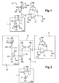
- This matrix is provided with a compensation structure intended to derive the major part of the common-mode electrical current passing through each of the bolometric detectors constituting it, and the principle of which is described in relation to the figure 2 .
- This compensation structure is unique for the entire matrix.
- this unique compensation structure 18 comprises a compensating bolometer 12, blind, and more precisely insensitive to infrared radiation, of resistance R comp , consisting of one or more elementary bolometers connected together.
- a power supply line 13 (VSK) is connected to one of the terminals of said resistor R comp .
- the other terminal of said resistor is connected to an injection transistor 14, so as to impose a reference current (I ref ) through the resistor R comp of the compensation bolometer 12 via a gate voltage (GSK) applied on the gate of said transistor.
- the blind bolometer 12 is constantly biased by means of the injection transistor 14 controlled by the gate voltage (GSK).
- a current-voltage converter 15 converts the reference current (I ref ) into a reference voltage (V ref ).
- This reference current (I ref ) is duplicated for each of the columns by means of a current mirror 16 disposed in said columns 5, each having a voltage converter (V ref ) - current (I ref ).
- a current integrator 19, formed of the amplifier 11 and the capacitance 10, is associated with each of the columns 5 of the matrix. It is intended to integrate the difference between the current flowing through the active bolometer 2 of the line being read and the reference current (I ref ) coming from the current mirror.
- the reference current (I ref ) is thus copied according to a current I 2 in all the columns of the matrix using the current mirror 16. Each of said columns has an additional current mirror 17 to return the direction of the current. current I 2 to a compensation current I 3 , in order to make the reference current (I ref ) compatible with the integration structure conventionally used.
- the current mirror 17 is only necessary if the active bolometer 2 is referenced to the detector's ground, a condition which is not necessary for the operation of the latter.
- VSK voltage
- V BUS voltage
- the embodiment as illustrated within the figure 2 may have limitations arising from the geometric and technological dispersion of the multiple MOS structures that it implements.
- the current mirror used to distribute the current on each column can not be matched by close drawing techniques, known to those skilled in the art, because the distance between the two branches of said current mirror can easily reach several millimeters in applications. common.
- the invention proposes, in the context of an embodiment of the invention illustrated within the figure 3 , to implement a low dispersion current mirror, and for this purpose, uses a differential mirror.
- two nearby transistors can be matched using known drawing techniques and judicious sizing of the transistors.
- the current from this voltage-current converter 23 is duplicated for each of the columns by means of the current mirror 16 also disposed in each of said columns 5.
- the reference current (I ref ) is copied according to a current II in all the columns of the matrix using the current mirror 16.
- Each of said columns has an additional current mirror 17 to return the direction of the current to a compensation current, in order to make the reference current (I ref ) compatible with the integration structure 19 previously described.
- the transistors forming part of the unique compensation structure 20 are very close to one another, and can therefore easily be matched.
- the transistors 27 and 28 are arranged in each column, and can therefore also be paired.
- the latter can not be matched to the transistors of the structure 20.
- the fact of working not with a single voltage Vref, but with a double voltage Vcmd + / Vcmd-differential, makes it possible to substantially limit the influence of space dispersions of the elemental electronic structures (MOS) distributed in each column, particularly in terms of voltage dispersion of threshold. In doing so, one gains in precision with respect to the embodiment of the figure 2 , in that in the latter, it is not possible to match the transistors 15 and 16, the latter being distributed by column.
- MOS elemental electronic structures
- the compensation bolometer of each column is suppressed. In doing so, it also suppresses the 1 / f noise that it generates in conventional detection structures, as illustrated in relation to the figure 1 .
- the noise in 1 / f is always present during the operation of the single compensation bolometer implemented in the invention, but on the one hand this noise can easily be reduced to a negligible amount by the implementation of a volume of bolometric material sufficiently high, at the cost of a consumed substrate surface very small compared to the total surface of the imager.
- this consumed surface remains in any case quite negligible compared to what is required for the construction of the compensating bolometric structures arranged in each column in the structures of the prior art of the figure 1 .
- the invention is particularly applicable in the field of image sensors with bolometric detection, whatever the optical detection band and the type of bolometric sensor used (in particular but not limited to amorphous silicon (a). -Si), vanadium oxides (Vox), metals (Ti)).
- the invention applies both to thermally controlled sensors and sensors operating at variable focal plane temperature.
- the intrinsic low-frequency low-noise column-based capability makes it possible to integrate the detectors made according to the invention into cameras that would be shutter-free (or, in the English expression, "shutter ").
- the invention remains perfectly compatible with traditional cameras provided with such a shutter. In doing so, it leads to a significant decrease in the cost of manufacturing such cameras, and a simplification of their implementation by the user.
Applications Claiming Priority (1)
| Application Number | Priority Date | Filing Date | Title |
|---|---|---|---|
| FR0756214A FR2918449B1 (fr) | 2007-07-02 | 2007-07-02 | Dispositif de detection de rayonnement infrarouge a detecteurs bolometriques |
Publications (2)
| Publication Number | Publication Date |
|---|---|
| EP2012100A1 EP2012100A1 (fr) | 2009-01-07 |
| EP2012100B1 true EP2012100B1 (fr) | 2012-11-14 |
Family
ID=39030895
Family Applications (1)
| Application Number | Title | Priority Date | Filing Date |
|---|---|---|---|
| EP08300224A Active EP2012100B1 (fr) | 2007-07-02 | 2008-06-17 | Dispositif de détection de rayonnement infrarouge à détecteurs bolométriques |
Country Status (6)
| Country | Link |
|---|---|
| US (1) | US7928387B2 (zh) |
| EP (1) | EP2012100B1 (zh) |
| CN (1) | CN101339074B (zh) |
| CA (1) | CA2632505C (zh) |
| FR (1) | FR2918449B1 (zh) |
| RU (1) | RU2454752C2 (zh) |
Families Citing this family (18)
| Publication number | Priority date | Publication date | Assignee | Title |
|---|---|---|---|---|
| IL167641A (en) * | 2005-03-24 | 2011-07-31 | Semi Conductor Devices An Elbit Systems Rafael Partnership | A system for measuring and compensating for changes in the case temperature in systems based on bulometers |
| IL167637A (en) * | 2005-03-24 | 2009-09-22 | Semi Conductor Devices An Elbi | Method and system for determining the rate of non uniformity of bolometer based systems |
| US8124937B2 (en) | 2009-01-15 | 2012-02-28 | Raytheon Company | System and method for athermal operation of a focal plane array |
| FR2944870B1 (fr) * | 2009-04-23 | 2011-06-24 | Commissariat Energie Atomique | Capteur a bolometre dote de moyens de regulation electrique des effets de la temperature |
| US9212951B2 (en) * | 2010-07-01 | 2015-12-15 | Panasonic Intellectual Property Management Co., Ltd. | Object detection device |
| FR2963850B1 (fr) * | 2010-08-10 | 2012-09-07 | Soc Fr Detecteurs Infrarouges Sofradir | Dispositif de detection a conditions de polarisation ameliorees |
| JP5331091B2 (ja) * | 2010-11-18 | 2013-10-30 | パナソニック株式会社 | 通信システム、送信装置、受信装置および通信方法 |
| FR2969763B1 (fr) * | 2010-12-22 | 2013-02-15 | Commissariat Energie Atomique | Systeme de mesure et imageur comportant un tel systeme |
| US8610062B2 (en) | 2011-03-24 | 2013-12-17 | Raytheon Company | Apparatus and method for multi-spectral imaging |
| CN102494781B (zh) * | 2011-12-14 | 2013-04-10 | 电子科技大学 | 一种读出电路偏置结构 |
| EP3598740B1 (en) | 2018-02-27 | 2022-09-14 | Shenzhen Goodix Technology Co., Ltd. | Image sensor and output compensation circuit of image sensor |
| FR3088512B1 (fr) * | 2018-11-09 | 2020-10-30 | Schneider Electric Ind Sas | Procede de traitement d'une image |
| CN109459141B (zh) * | 2018-12-18 | 2024-04-30 | 山西德润翔电力科技有限公司 | 双色红外测温装置 |
| CN110296761B (zh) * | 2019-07-25 | 2020-06-05 | 北京安酷智芯科技有限公司 | 一种读出电路 |
| US10827090B1 (en) * | 2019-09-16 | 2020-11-03 | Innolux Corporation | Electronic device and method for operating electronic device |
| CN111579095B (zh) * | 2020-04-30 | 2021-11-30 | 南京雷石电子科技有限公司 | 一种车载低温红外探测系统 |
| IL275896B (en) * | 2020-07-07 | 2022-07-01 | Frank Amit | Imaging device and method |
| CN112082661B (zh) * | 2020-07-27 | 2021-09-14 | 上海集成电路研发中心有限公司 | 一种基于像元合并的红外探测器结构及其合并方法 |
Family Cites Families (24)
| Publication number | Priority date | Publication date | Assignee | Title |
|---|---|---|---|---|
| GB9404111D0 (en) * | 1994-03-03 | 1994-04-20 | Philips Electronics Uk Ltd | A charge storage device |
| US5784178A (en) * | 1996-03-06 | 1998-07-21 | Dyna Image Corporation | High performance contact image sensor |
| US6141048A (en) * | 1996-08-19 | 2000-10-31 | Eastman Kodak Company | Compact image capture device |
| JPH10122957A (ja) * | 1996-10-22 | 1998-05-15 | Nikon Corp | 熱型赤外線イメージセンサ |
| DE69825402T2 (de) * | 1997-03-12 | 2005-08-04 | Seiko Epson Corp. | Pixelschaltung, anzeigevorrichtung und elektronische apparatur mit stromgesteuerter lichtemittierender vorrichtung |
| CN1280738A (zh) * | 1997-09-26 | 2001-01-17 | 英国国防部 | 传感器设备 |
| US6384413B1 (en) * | 1998-10-13 | 2002-05-07 | California Institute Of Technology | Focal plane infrared readout circuit |
| FR2788129B1 (fr) * | 1998-12-30 | 2001-02-16 | Commissariat Energie Atomique | Detecteur bolometrique a antenne |
| US6704050B1 (en) * | 1999-04-23 | 2004-03-09 | Polaroid Corporation | Active-pixel image sensing device with linear mode voltage to current conversion |
| US6583416B1 (en) * | 1999-11-15 | 2003-06-24 | Sarnoff Corporation | Uncooled IR detector array having improved temperature stability and reduced fixed pattern noise |
| JP2001245215A (ja) * | 2000-01-11 | 2001-09-07 | Agilent Technol Inc | 改善された基準信号を有するアクティブピクセルセンサ |
| JP3866069B2 (ja) * | 2001-09-26 | 2007-01-10 | 株式会社東芝 | 赤外線固体撮像装置 |
| US6812465B2 (en) * | 2002-02-27 | 2004-11-02 | Indigo Systems Corporation | Microbolometer focal plane array methods and circuitry |
| JP5122131B2 (ja) * | 2003-04-25 | 2013-01-16 | 統寶光電股▲ふん▼有限公司 | アクティブマトリクスディスプレイパネルを駆動する方法および装置 |
| US7119334B2 (en) * | 2003-11-03 | 2006-10-10 | Namal Technologies Ltd. | Thermal imaging system and method |
| FR2862160B1 (fr) * | 2003-11-10 | 2006-05-12 | Ulis | Dispositif de detection de rayonnements infrarouges a detecteurs bolometriques |
| US20060007204A1 (en) * | 2004-06-29 | 2006-01-12 | Damoder Reddy | System and method for a long-life luminance feedback stabilized display panel |
| GB0500111D0 (en) * | 2005-01-06 | 2005-02-09 | Koninkl Philips Electronics Nv | Inkjet print head |
| US7616231B2 (en) * | 2005-01-06 | 2009-11-10 | Goodrich Corporation | CMOS active pixel sensor with improved dynamic range and method of operation for object motion detection |
| JP2006292594A (ja) * | 2005-04-12 | 2006-10-26 | Nec Electronics Corp | 赤外線検知器 |
| WO2007015235A1 (en) * | 2005-08-04 | 2007-02-08 | Semi-Conductor Devices-An Elbit Systems-Rafael Partnership | Circuitry for balancing a differential type focal plane array of bolometer based infra-red detectors |
| JP4654857B2 (ja) * | 2005-09-26 | 2011-03-23 | ソニー株式会社 | Da変換装置、ad変換装置、半導体装置 |
| US7435961B2 (en) * | 2006-03-17 | 2008-10-14 | Lucent Technologies Inc. | Imaging sensor |
| JP4901320B2 (ja) * | 2006-06-13 | 2012-03-21 | 三菱電機株式会社 | 2波長イメージセンサ |
-
2007
- 2007-07-02 FR FR0756214A patent/FR2918449B1/fr not_active Expired - Fee Related
-
2008
- 2008-05-28 US US12/127,976 patent/US7928387B2/en not_active Expired - Fee Related
- 2008-05-29 CA CA2632505A patent/CA2632505C/fr active Active
- 2008-06-09 RU RU2008123479/28A patent/RU2454752C2/ru active
- 2008-06-10 CN CN2008101110592A patent/CN101339074B/zh active Active
- 2008-06-17 EP EP08300224A patent/EP2012100B1/fr active Active
Also Published As
| Publication number | Publication date |
|---|---|
| RU2454752C2 (ru) | 2012-06-27 |
| US20090008555A1 (en) | 2009-01-08 |
| US7928387B2 (en) | 2011-04-19 |
| FR2918449B1 (fr) | 2010-05-21 |
| CA2632505A1 (fr) | 2009-01-02 |
| RU2008123479A (ru) | 2009-12-20 |
| CN101339074B (zh) | 2011-12-28 |
| CA2632505C (fr) | 2016-09-13 |
| EP2012100A1 (fr) | 2009-01-07 |
| CN101339074A (zh) | 2009-01-07 |
| FR2918449A1 (fr) | 2009-01-09 |
Similar Documents
| Publication | Publication Date | Title |
|---|---|---|
| EP2012100B1 (fr) | Dispositif de détection de rayonnement infrarouge à détecteurs bolométriques | |
| EP2012101B1 (fr) | Dispositif de détection de rayonnement électromagnétique, en particulier infrarouge | |
| CA2647365C (fr) | Dispositif pour la detection d'un rayonnement electromagnetique comportant un bolometre resistif d'imagerie, systeme comprenant une matrice de tels dispositifs et procede de lecture d'un bolometre d'imagerie d'un tel systeme | |
| EP2071309B1 (fr) | Dispositif pour la détection d'un rayonnement infrarouge comportant un bolomètre résistif d'imagerie, système comprenant une matrice de tels bolomètres, et procédé de lecture d'un bolomètre d'imagerie intégré dans un tel système | |
| EP2770312B1 (fr) | Détecteur bolométrique à polarisation adaptative en température | |
| EP2208976B1 (fr) | Dispositif pour la détection d'un rayonnement électromagnétique | |
| EP2163871A1 (fr) | Dispositif pour la détection d'un rayonnement infrarouge comportant un bolomètre et procédé de lecture d'un tel bolomètre intégré dans une matrice de bolomètres | |
| EP2425220A1 (fr) | Systeme et procede de dectection de rayonnement infrarouge | |
| FR3020906A1 (fr) | Dispositif haute dynamique pour l'integration d'un courant electrique | |
| FR2875336A1 (fr) | Dispositif de detection de rayonnements infrarouges a detecteurs bolometriques | |
| EP2209305B1 (fr) | Dispositif pour la détection d'un rayonnement électromagnétique | |
| EP0354106B1 (fr) | Circuit d'élimination du bruit, intégré dans un détecteur d'images à l'état solide | |
| EP2037241A1 (fr) | Dispositif de détection d'un rayonnement électromagnétique à limitation de courant | |
| CA2452627A1 (fr) | Dispositif de detection de rayonnements electromagnetiques | |
| WO2010106286A1 (fr) | Procede de reglage d'un circuit de detection de rayonnements | |
| FR2942074A1 (fr) | Dispositif pour la detection d'un rayonnement electromagnetique, et notamment infrarouge | |
| EP4025886A1 (fr) | Capteur infrarouge a capture instantanee |
Legal Events
| Date | Code | Title | Description |
|---|---|---|---|
| PUAI | Public reference made under article 153(3) epc to a published international application that has entered the european phase |
Free format text: ORIGINAL CODE: 0009012 |
|
| AK | Designated contracting states |
Kind code of ref document: A1 Designated state(s): AT BE BG CH CY CZ DE DK EE ES FI FR GB GR HR HU IE IS IT LI LT LU LV MC MT NL NO PL PT RO SE SI SK TR |
|
| AX | Request for extension of the european patent |
Extension state: AL BA MK RS |
|
| 17P | Request for examination filed |
Effective date: 20090126 |
|
| 17Q | First examination report despatched |
Effective date: 20090225 |
|
| AKX | Designation fees paid |
Designated state(s): DE FR GB IT SE |
|
| GRAP | Despatch of communication of intention to grant a patent |
Free format text: ORIGINAL CODE: EPIDOSNIGR1 |
|
| RIC1 | Information provided on ipc code assigned before grant |
Ipc: H04N 5/335 20110101ALI20120807BHEP Ipc: G01J 5/22 20060101AFI20120807BHEP Ipc: H04N 5/33 20060101ALI20120807BHEP |
|
| GRAS | Grant fee paid |
Free format text: ORIGINAL CODE: EPIDOSNIGR3 |
|
| GRAA | (expected) grant |
Free format text: ORIGINAL CODE: 0009210 |
|
| AK | Designated contracting states |
Kind code of ref document: B1 Designated state(s): DE FR GB IT SE |
|
| REG | Reference to a national code |
Ref country code: GB Ref legal event code: FG4D Free format text: NOT ENGLISH |
|
| REG | Reference to a national code |
Ref country code: SE Ref legal event code: TRGR |
|
| REG | Reference to a national code |
Ref country code: DE Ref legal event code: R096 Ref document number: 602008020083 Country of ref document: DE Effective date: 20130110 |
|
| PLBE | No opposition filed within time limit |
Free format text: ORIGINAL CODE: 0009261 |
|
| STAA | Information on the status of an ep patent application or granted ep patent |
Free format text: STATUS: NO OPPOSITION FILED WITHIN TIME LIMIT |
|
| 26N | No opposition filed |
Effective date: 20130815 |
|
| REG | Reference to a national code |
Ref country code: DE Ref legal event code: R097 Ref document number: 602008020083 Country of ref document: DE Effective date: 20130815 |
|
| PGFP | Annual fee paid to national office [announced via postgrant information from national office to epo] |
Ref country code: IT Payment date: 20140619 Year of fee payment: 7 |
|
| PG25 | Lapsed in a contracting state [announced via postgrant information from national office to epo] |
Ref country code: IT Free format text: LAPSE BECAUSE OF NON-PAYMENT OF DUE FEES Effective date: 20150617 |
|
| REG | Reference to a national code |
Ref country code: FR Ref legal event code: PLFP Year of fee payment: 9 |
|
| REG | Reference to a national code |
Ref country code: FR Ref legal event code: PLFP Year of fee payment: 10 |
|
| REG | Reference to a national code |
Ref country code: FR Ref legal event code: PLFP Year of fee payment: 11 |
|
| PGFP | Annual fee paid to national office [announced via postgrant information from national office to epo] |
Ref country code: SE Payment date: 20220623 Year of fee payment: 15 Ref country code: GB Payment date: 20220616 Year of fee payment: 15 Ref country code: DE Payment date: 20220607 Year of fee payment: 15 |
|
| PGFP | Annual fee paid to national office [announced via postgrant information from national office to epo] |
Ref country code: FR Payment date: 20220628 Year of fee payment: 15 |
|
| REG | Reference to a national code |
Ref country code: DE Ref legal event code: R119 Ref document number: 602008020083 Country of ref document: DE |
|
| REG | Reference to a national code |
Ref country code: SE Ref legal event code: EUG |
|
| GBPC | Gb: european patent ceased through non-payment of renewal fee |
Effective date: 20230617 |
|
| PG25 | Lapsed in a contracting state [announced via postgrant information from national office to epo] |
Ref country code: DE Free format text: LAPSE BECAUSE OF NON-PAYMENT OF DUE FEES Effective date: 20240103 Ref country code: GB Free format text: LAPSE BECAUSE OF NON-PAYMENT OF DUE FEES Effective date: 20230617 |