EP2012100B1 - Device for detecting infrared radiation using bolometric detectors - Google Patents
Device for detecting infrared radiation using bolometric detectors Download PDFInfo
- Publication number
- EP2012100B1 EP2012100B1 EP08300224A EP08300224A EP2012100B1 EP 2012100 B1 EP2012100 B1 EP 2012100B1 EP 08300224 A EP08300224 A EP 08300224A EP 08300224 A EP08300224 A EP 08300224A EP 2012100 B1 EP2012100 B1 EP 2012100B1
- Authority
- EP
- European Patent Office
- Prior art keywords
- current
- array
- column
- bolometer
- bolometers
- Prior art date
- Legal status (The legal status is an assumption and is not a legal conclusion. Google has not performed a legal analysis and makes no representation as to the accuracy of the status listed.)
- Active
Links
- 230000005855 radiation Effects 0.000 title claims description 10
- 239000000758 substrate Substances 0.000 claims description 18
- 238000002347 injection Methods 0.000 claims description 11
- 239000007924 injection Substances 0.000 claims description 11
- 230000010354 integration Effects 0.000 claims description 9
- 238000004519 manufacturing process Methods 0.000 claims description 2
- 230000005670 electromagnetic radiation Effects 0.000 claims 1
- 239000006185 dispersion Substances 0.000 description 18
- 239000011159 matrix material Substances 0.000 description 17
- 101150065984 Comp gene Proteins 0.000 description 13
- 238000001514 detection method Methods 0.000 description 9
- 239000000463 material Substances 0.000 description 8
- 229910021417 amorphous silicon Inorganic materials 0.000 description 7
- 238000000034 method Methods 0.000 description 7
- 230000003287 optical effect Effects 0.000 description 6
- 230000000694 effects Effects 0.000 description 5
- 238000005516 engineering process Methods 0.000 description 5
- 238000010276 construction Methods 0.000 description 4
- 238000003384 imaging method Methods 0.000 description 4
- 238000006243 chemical reaction Methods 0.000 description 3
- 230000005284 excitation Effects 0.000 description 3
- 230000004907 flux Effects 0.000 description 3
- 239000012528 membrane Substances 0.000 description 3
- IJGRMHOSHXDMSA-UHFFFAOYSA-N Atomic nitrogen Chemical compound N#N IJGRMHOSHXDMSA-UHFFFAOYSA-N 0.000 description 2
- XUIMIQQOPSSXEZ-UHFFFAOYSA-N Silicon Chemical compound [Si] XUIMIQQOPSSXEZ-UHFFFAOYSA-N 0.000 description 2
- XHCLAFWTIXFWPH-UHFFFAOYSA-N [O-2].[O-2].[O-2].[O-2].[O-2].[V+5].[V+5] Chemical compound [O-2].[O-2].[O-2].[O-2].[O-2].[V+5].[V+5] XHCLAFWTIXFWPH-UHFFFAOYSA-N 0.000 description 2
- 230000009471 action Effects 0.000 description 2
- 238000009826 distribution Methods 0.000 description 2
- 238000003331 infrared imaging Methods 0.000 description 2
- 238000009413 insulation Methods 0.000 description 2
- 229910052751 metal Inorganic materials 0.000 description 2
- 239000002184 metal Substances 0.000 description 2
- 230000010287 polarization Effects 0.000 description 2
- 238000007781 pre-processing Methods 0.000 description 2
- 238000004886 process control Methods 0.000 description 2
- 229910052710 silicon Inorganic materials 0.000 description 2
- 239000010703 silicon Substances 0.000 description 2
- 230000006641 stabilisation Effects 0.000 description 2
- 238000011105 stabilization Methods 0.000 description 2
- 229910001935 vanadium oxide Inorganic materials 0.000 description 2
- 241001080024 Telles Species 0.000 description 1
- 240000008042 Zea mays Species 0.000 description 1
- 230000002745 absorbent Effects 0.000 description 1
- 239000002250 absorbent Substances 0.000 description 1
- 238000010521 absorption reaction Methods 0.000 description 1
- 238000003491 array Methods 0.000 description 1
- 239000003990 capacitor Substances 0.000 description 1
- 239000000969 carrier Substances 0.000 description 1
- 238000012512 characterization method Methods 0.000 description 1
- 238000001816 cooling Methods 0.000 description 1
- 230000001627 detrimental effect Effects 0.000 description 1
- 230000037213 diet Effects 0.000 description 1
- 235000005911 diet Nutrition 0.000 description 1
- 238000010438 heat treatment Methods 0.000 description 1
- 238000002955 isolation Methods 0.000 description 1
- 239000007788 liquid Substances 0.000 description 1
- 239000007769 metal material Substances 0.000 description 1
- 150000002739 metals Chemical class 0.000 description 1
- 229910052757 nitrogen Inorganic materials 0.000 description 1
- 230000008569 process Effects 0.000 description 1
- 230000001105 regulatory effect Effects 0.000 description 1
- 230000004044 response Effects 0.000 description 1
- 230000000717 retained effect Effects 0.000 description 1
- 229920006395 saturated elastomer Polymers 0.000 description 1
- 239000004065 semiconductor Substances 0.000 description 1
- 238000004513 sizing Methods 0.000 description 1
- 230000003595 spectral effect Effects 0.000 description 1
- 230000003068 static effect Effects 0.000 description 1
- 238000004861 thermometry Methods 0.000 description 1
Images

Classifications
-
- G—PHYSICS
- G01—MEASURING; TESTING
- G01J—MEASUREMENT OF INTENSITY, VELOCITY, SPECTRAL CONTENT, POLARISATION, PHASE OR PULSE CHARACTERISTICS OF INFRARED, VISIBLE OR ULTRAVIOLET LIGHT; COLORIMETRY; RADIATION PYROMETRY
- G01J5/00—Radiation pyrometry, e.g. infrared or optical thermometry
- G01J5/10—Radiation pyrometry, e.g. infrared or optical thermometry using electric radiation detectors
- G01J5/20—Radiation pyrometry, e.g. infrared or optical thermometry using electric radiation detectors using resistors, thermistors or semiconductors sensitive to radiation, e.g. photoconductive devices
- G01J5/22—Electrical features thereof
-
- H—ELECTRICITY
- H04—ELECTRIC COMMUNICATION TECHNIQUE
- H04N—PICTORIAL COMMUNICATION, e.g. TELEVISION
- H04N25/00—Circuitry of solid-state image sensors [SSIS]; Control thereof
- H04N25/60—Noise processing, e.g. detecting, correcting, reducing or removing noise
- H04N25/63—Noise processing, e.g. detecting, correcting, reducing or removing noise applied to dark current
-
- H—ELECTRICITY
- H04—ELECTRIC COMMUNICATION TECHNIQUE
- H04N—PICTORIAL COMMUNICATION, e.g. TELEVISION
- H04N25/00—Circuitry of solid-state image sensors [SSIS]; Control thereof
- H04N25/60—Noise processing, e.g. detecting, correcting, reducing or removing noise
- H04N25/67—Noise processing, e.g. detecting, correcting, reducing or removing noise applied to fixed-pattern noise, e.g. non-uniformity of response
- H04N25/671—Noise processing, e.g. detecting, correcting, reducing or removing noise applied to fixed-pattern noise, e.g. non-uniformity of response for non-uniformity detection or correction
- H04N25/672—Noise processing, e.g. detecting, correcting, reducing or removing noise applied to fixed-pattern noise, e.g. non-uniformity of response for non-uniformity detection or correction between adjacent sensors or output registers for reading a single image
-
- H—ELECTRICITY
- H04—ELECTRIC COMMUNICATION TECHNIQUE
- H04N—PICTORIAL COMMUNICATION, e.g. TELEVISION
- H04N5/00—Details of television systems
- H04N5/30—Transforming light or analogous information into electric information
- H04N5/33—Transforming infrared radiation
Definitions
- the present invention relates to a device for detecting infrared radiation using bolometric detectors. It particularly finds its field of application in infrared imaging.
- infrared detectors In the field of infrared detectors, it is known to use devices arranged in matrix form, and capable of operating at ambient temperature, that is to say not requiring cooling at very low temperatures, unlike the devices of FIG. detection called “quantum infrared detectors" which, they require operation at a very low temperature, typically that of liquid nitrogen.
- the detectors intended for infrared imaging are conventionally produced in the form of a matrix of elementary detectors in one or two dimensions, said matrix being formed so-called “monolithic” or carried on a substrate generally made of silicon, in which are consisting of means for sequentially addressing the elementary detectors and means for electrical excitation and pre-processing of the electrical signals generated by these elementary detectors. These means of sequential addressing, electrical excitation and pre-processing are thus formed on the substrate and constitute a read circuit.
- the scene is projected through an optics adapted to the matrix of elementary detectors, each of them constituting an image point or pixel, and clocked electrical stimuli are applied by the intermediate of the reading circuit to each of the elementary detectors, or to each row of such detectors, in order to obtain an electrical signal constituting the image of the temperature reached by each of said elementary detectors.
- This signal is processed more or less elaborately by the read circuit, then possibly by an electronic device outside the housing to generate the thermal image of the scene observed.
- the essential difficulty of implementing the bolometric detectors lies in the very small relative variation in their electrical resistance, representative of the local temperature variations of an observed scene, compared with the average value of these resistors.
- the residual temperature fluctuations of the substrate, under ordinary conditions of thermal stabilization, especially if the detector is free of such a thermal stabilization system, a situation that is more and more frequent in this type of detector in order to reduce its cost. produce accordingly on the signal from the bolometer a useless component, which affects the quality of the signal.
- the substrate is traditionally thermally regulated.
- so-called “compensation” structures are implemented to attenuate the effects of the temperature of the focal plane on the response of the circuit.
- These structures usually so-called “blind” bolometers, that is to say, insensitive to the incident optical flux, but sensitive to the temperature of the substrate, are used to generate a so-called compensation current, which is subtracted from the current coming from the bolometers.
- imaging, ie detection bolometers thanks to the configuration of the electronic circuit.
- these compensation structures are constructed so as to have a very low thermal resistance with respect to the substrate, unlike the imaging bolometers.
- the compensation structures being essentially at the temperature of the reading circuit, and therefore of the focal plane, a significant rejection of any temperature fluctuations of the latter is obtained directly. It is known to arrange these compensation structures "identically" repeatedly in each column of the matrix, so as to limit the complexity and overall size of the circuit.
- Each column of bolometers is sequentially compensated, during the line-by-line electronic scanning of the image, using the same compensation structure.
- the compensation structures naturally have a spatial dispersion of resistance, related to the technological processes used in their development (which usually belong to the semiconductor industry).
- blind bolometers as well as imaging bolometers, as well as certain functions of the reading circuit, exhibit noise phenomena in general, and noise called "in 1 / f" in particular.
- the 1 / f noise is typically the source of a low-frequency drift, and particularly very low frequency, of the output level of the sensors, which affects the quality of the imager. It results from the column arrangement of the compensation, a negative impact on the quality of the image, because of the low frequency variations, asynchronous between columns, of the compensated signal.
- compensation algorithms must generally be developed and applied at the output of the imager in order to improve the image quality.
- detector arrays employing a single compensation structure for a large number of pixels are described in EP 1117250 .
- the operation takes place in two phases.
- the polarization of the bolometers is chosen so as to ensure both a good dynamic output signal and effective compensation.
- This reading system has certain limitations related to the reproduction of the column compensation pattern on the read circuit. Indeed, each column has a compensation bolometer and its PMOS injection transistor. The imperfect reproduction of these different elements from one column to another, inherent to the intrinsic spatial dispersions of the construction technologies used, gives rise to a dispersion in the efficiency of the compensation. These dispersions Statistics result in a non-uniform compensation current from one column to the other, showing visible columnar contrasts, thus affecting the available signal.
- the noise power provided by the compensation structure increases by a constant increment for each additional decade of frequency between the two integration terminals f min and f max .
- the compensating bolometers are permanently polarized, so the lower limit of frequency f min of the integration can therefore be considered very low, insofar as the component remains energized for an extended period, once the detector is activated.
- the column perturbations (expressed by those skilled in the art analytically by the noise power above) are manifested as an "offset" or shift, at first order invariant from one image to the other, if the we consider frequencies lower than the frame frequency, but variable over a longer period of time, when the camera incorporating such a detector has been in operation for several minutes.
- the market tendency towards an increase in the number of points of the bolometric sensors makes that the compensation bolometers of each column, effective on small imagers as absolute reference of temperature, act like "local" references of temperatures, from the point of view of the most distant active bolometers.
- a thermal source of any origin for example locally more or less dissipative circuitry elements, can influence all or part of the compensation bolometers, the latter will be influenced in relation to their distance from the source of disturbance, and thus reproduce a compensation current distribution unsuited to the substrate temperature dispersions seen by the sensitive bolometers, not concerned, or in general in a different manner, by said thermal source.
- the present invention aims a detection device implementing a single compensation structure, and to overcome the limitations of image quality, particularly related to differences in columnar contrast and spatial dispersions of elementary electronic structures distributed in each column.
- This infrared detection device comprises the features of claim 1.
- the entire bolometer array is compensated by a single structure, thereby avoiding columnar contrasts observable with the detectors of the prior art.
- the blind bolometer may consist of one or more elementary blind bolometers connected together. This or these blind bolometers are made similar to the active bolometers, but have negligible thermal resistance relative to the substrate.
- the simultaneous copying means for each column of the matrix of said reference current are constituted by current mirrors disposed in each of said columns, said mirrors each comprising a voltage-current converter.
- the current mirror used in each of the columns is a differential current mirror.
- the bolometric detector matrix is formed on a silicon substrate, in which the read circuit is formed.
- This substrate is traditionally covered, at the level of the active structures, ie directly above the optically sensitive zone, with a reflective metal layer.
- the latter is intended, in known manner, to form a quarter-wave cavity between the substrate and the absorbent parts of the detector.
- the optically active zones are formed by a tiling of suspended membranes, comprising, above the reading circuit, a bolometric material. These membranes are supported by means of essentially vertical, electrically conductive structures. These structures, made using a metallic material, are further intended to bring the excitation potentials generated by the reading circuit to the conductive parts, also called electrodes, of the membrane of each elementary bolometric detector, via elongate structures, also electrically conductive, but thermally resistant.
- thermal insulation is intended to allow the heating of the bolometer under the effect of infra-red radiation to be detected.
- the read circuit sequentially applies an electric current that passes through the suspended structure. This current flows through a material whose resistivity varies with temperature, which is called a bolometric material.
- a material whose resistivity varies with temperature.
- the most common materials for this purpose are vanadium oxide (generic formula VO x ) and amorphous silicon (a-Si).
- This matrix is provided with a compensation structure intended to derive the major part of the common-mode electrical current passing through each of the bolometric detectors constituting it, and the principle of which is described in relation to the figure 2 .
- This compensation structure is unique for the entire matrix.
- this unique compensation structure 18 comprises a compensating bolometer 12, blind, and more precisely insensitive to infrared radiation, of resistance R comp , consisting of one or more elementary bolometers connected together.
- a power supply line 13 (VSK) is connected to one of the terminals of said resistor R comp .
- the other terminal of said resistor is connected to an injection transistor 14, so as to impose a reference current (I ref ) through the resistor R comp of the compensation bolometer 12 via a gate voltage (GSK) applied on the gate of said transistor.
- the blind bolometer 12 is constantly biased by means of the injection transistor 14 controlled by the gate voltage (GSK).
- a current-voltage converter 15 converts the reference current (I ref ) into a reference voltage (V ref ).
- This reference current (I ref ) is duplicated for each of the columns by means of a current mirror 16 disposed in said columns 5, each having a voltage converter (V ref ) - current (I ref ).
- a current integrator 19, formed of the amplifier 11 and the capacitance 10, is associated with each of the columns 5 of the matrix. It is intended to integrate the difference between the current flowing through the active bolometer 2 of the line being read and the reference current (I ref ) coming from the current mirror.
- the reference current (I ref ) is thus copied according to a current I 2 in all the columns of the matrix using the current mirror 16. Each of said columns has an additional current mirror 17 to return the direction of the current. current I 2 to a compensation current I 3 , in order to make the reference current (I ref ) compatible with the integration structure conventionally used.
- the current mirror 17 is only necessary if the active bolometer 2 is referenced to the detector's ground, a condition which is not necessary for the operation of the latter.
- VSK voltage
- V BUS voltage
- the embodiment as illustrated within the figure 2 may have limitations arising from the geometric and technological dispersion of the multiple MOS structures that it implements.
- the current mirror used to distribute the current on each column can not be matched by close drawing techniques, known to those skilled in the art, because the distance between the two branches of said current mirror can easily reach several millimeters in applications. common.
- the invention proposes, in the context of an embodiment of the invention illustrated within the figure 3 , to implement a low dispersion current mirror, and for this purpose, uses a differential mirror.
- two nearby transistors can be matched using known drawing techniques and judicious sizing of the transistors.
- the current from this voltage-current converter 23 is duplicated for each of the columns by means of the current mirror 16 also disposed in each of said columns 5.
- the reference current (I ref ) is copied according to a current II in all the columns of the matrix using the current mirror 16.
- Each of said columns has an additional current mirror 17 to return the direction of the current to a compensation current, in order to make the reference current (I ref ) compatible with the integration structure 19 previously described.
- the transistors forming part of the unique compensation structure 20 are very close to one another, and can therefore easily be matched.
- the transistors 27 and 28 are arranged in each column, and can therefore also be paired.
- the latter can not be matched to the transistors of the structure 20.
- the fact of working not with a single voltage Vref, but with a double voltage Vcmd + / Vcmd-differential, makes it possible to substantially limit the influence of space dispersions of the elemental electronic structures (MOS) distributed in each column, particularly in terms of voltage dispersion of threshold. In doing so, one gains in precision with respect to the embodiment of the figure 2 , in that in the latter, it is not possible to match the transistors 15 and 16, the latter being distributed by column.
- MOS elemental electronic structures
- the compensation bolometer of each column is suppressed. In doing so, it also suppresses the 1 / f noise that it generates in conventional detection structures, as illustrated in relation to the figure 1 .
- the noise in 1 / f is always present during the operation of the single compensation bolometer implemented in the invention, but on the one hand this noise can easily be reduced to a negligible amount by the implementation of a volume of bolometric material sufficiently high, at the cost of a consumed substrate surface very small compared to the total surface of the imager.
- this consumed surface remains in any case quite negligible compared to what is required for the construction of the compensating bolometric structures arranged in each column in the structures of the prior art of the figure 1 .
- the invention is particularly applicable in the field of image sensors with bolometric detection, whatever the optical detection band and the type of bolometric sensor used (in particular but not limited to amorphous silicon (a). -Si), vanadium oxides (Vox), metals (Ti)).
- the invention applies both to thermally controlled sensors and sensors operating at variable focal plane temperature.
- the intrinsic low-frequency low-noise column-based capability makes it possible to integrate the detectors made according to the invention into cameras that would be shutter-free (or, in the English expression, "shutter ").
- the invention remains perfectly compatible with traditional cameras provided with such a shutter. In doing so, it leads to a significant decrease in the cost of manufacturing such cameras, and a simplification of their implementation by the user.
Description
La présente invention concerne un dispositif de détection de rayonnement infrarouge mettant en oeuvre des détecteurs bolométriques. Elle trouve notamment son domaine d'application dans l'imagerie infrarouge.The present invention relates to a device for detecting infrared radiation using bolometric detectors. It particularly finds its field of application in infrared imaging.
Dans le domaine des détecteurs infrarouges, il est connu d'utiliser des dispositifs agencés sous forme matricielle, et susceptibles de fonctionner à température ambiante, c'est-à-dire ne nécessitant pas de refroidissement à de très basses températures, contrairement aux dispositifs de détection appelés "détecteurs infrarouge quantiques" qui eux, nécessitent un fonctionnement à très basse température, typiquement celle de l'azote liquide.In the field of infrared detectors, it is known to use devices arranged in matrix form, and capable of operating at ambient temperature, that is to say not requiring cooling at very low temperatures, unlike the devices of FIG. detection called "quantum infrared detectors" which, they require operation at a very low temperature, typically that of liquid nitrogen.
Ces détecteurs non refroidis utilisent traditionnellement la variation d'une grandeur physique d'un matériau approprié, en fonction de la température, au voisinage de 300K. Dans le cas des détecteurs bolométriques, cette grandeur physique est la résistivité électrique.These uncooled detectors traditionally use the variation of a physical quantity of a suitable material, depending on the temperature, in the vicinity of 300K. In the case of bolometric detectors, this physical quantity is the electrical resistivity.
Un tel détecteur non refroidi associe généralement :
- des moyens d'absorption du rayonnement infrarouge et de conversion de celui-ci en chaleur;
- des moyens d'isolation thermique du détecteur, de telle sorte à permettre à celui-ci de s'échauffer sous l'action du rayonnement infrarouge à détecter ;
- des moyens de thermométrie qui, dans le cadre d'un détecteur bolométrique, mettent en oeuvre un élément résistif ;
- et des moyens de lecture des signaux électriques fournis par les moyens de thermométrie.
- means for absorbing infrared radiation and converting it into heat;
- thermal insulation means of the detector, so as to allow it to heat up under the action of infrared radiation to be detected;
- thermometric means which, in the context of a bolometric detector, implement a resistive element;
- and means for reading the electrical signals supplied by the thermometry means.
Les détecteurs destinés à l'imagerie infrarouge sont classiquement réalisés sous la forme d'une matrice de détecteurs élémentaires selon une ou deux dimensions, ladite matrice étant formée de manière dite "monolithique" ou reportée sur un substrat généralement réalisé en silicium, dans lequel sont constitués des moyens d'adressage séquentiel des détecteurs élémentaires et des moyens d'excitation électrique et de pré-traitement des signaux électriques générés par ces détecteurs élémentaires. Ces moyens d'adressage séquentiel, d'excitation électrique et de pré-traitement sont donc formés sur le substrat et constituent un circuit de lecture.The detectors intended for infrared imaging are conventionally produced in the form of a matrix of elementary detectors in one or two dimensions, said matrix being formed so-called "monolithic" or carried on a substrate generally made of silicon, in which are consisting of means for sequentially addressing the elementary detectors and means for electrical excitation and pre-processing of the electrical signals generated by these elementary detectors. These means of sequential addressing, electrical excitation and pre-processing are thus formed on the substrate and constitute a read circuit.
Pour obtenir une scène par l'intermédiaire de ce détecteur, on projette la scène à travers une optique adaptée sur la matrice de détecteurs élémentaires, chacun d'entre eux constituant un point image ou pixel, et des stimuli électriques cadencés sont appliqués par l'intermédiaire du circuit de lecture à chacun des détecteurs élémentaires, ou à chaque rangée de tels détecteurs, afin d'obtenir un signal électrique constituant l'image de la température atteinte par chacun desdits détecteurs élémentaires. Ce signal est traité de manière plus ou moins élaborée par le circuit de lecture, puis éventuellement par un dispositif électronique extérieur au boîtier afin de générer l'image thermique de la scène observée.To obtain a scene via this detector, the scene is projected through an optics adapted to the matrix of elementary detectors, each of them constituting an image point or pixel, and clocked electrical stimuli are applied by the intermediate of the reading circuit to each of the elementary detectors, or to each row of such detectors, in order to obtain an electrical signal constituting the image of the temperature reached by each of said elementary detectors. This signal is processed more or less elaborately by the read circuit, then possibly by an electronic device outside the housing to generate the thermal image of the scene observed.
La difficulté essentielle de mise en oeuvre des détecteurs bolométriques réside dans la très faible variation relative de leur résistance électrique, représentative des variations locales de température d'une scène observée, par rapport à la valeur moyenne de ces résistances.The essential difficulty of implementing the bolometric detectors lies in the very small relative variation in their electrical resistance, representative of the local temperature variations of an observed scene, compared with the average value of these resistors.
La présence par construction d'une résistance thermique finie entre le bolomètre et le substrat, implique que la température du bolomètre est influencée par la température du substrat, et ceci de manière beaucoup plus sensible que les variations de température dues au flux incident, qui seules sont à prendre en considération du point de vue signal à détecter. Les fluctuations résiduelles de température du substrat, dans des conditions ordinaires de stabilisation thermique, a fortiori si le détecteur est exempt d'un tel système de stabilisation thermique, situation de plus en plus fréquente dans ce type de détecteurs afin d'en diminuer le coût, produisent en conséquence sur le signal issu du bolomètre une composante inutile, qui nuit à la qualité du signal. Pour éviter ou au moins limiter cet effet, le substrat est traditionnellement régulé thermiquement.The presence by construction of a finite thermal resistance between the bolometer and the substrate, implies that the temperature of the bolometer is influenced by the temperature of the substrate, and this much more sensitive than the temperature variations due to the incident flux, which alone are to take into consideration the signal point of view to be detected. The residual temperature fluctuations of the substrate, under ordinary conditions of thermal stabilization, especially if the detector is free of such a thermal stabilization system, a situation that is more and more frequent in this type of detector in order to reduce its cost. , produce accordingly on the signal from the bolometer a useless component, which affects the quality of the signal. To avoid or at least limit this effect, the substrate is traditionally thermally regulated.
De plus, des structures dites « de compensation » sont mises en oeuvre pour atténuer les effets de la température du plan focal sur la réponse du circuit. Ces structures, usuellement des bolomètres dits « aveugles », c'est-à-dire insensibles au flux optique incident, mais sensibles à la température du substrat, sont utilisées pour générer un courant dit de compensation, qui est soustrait du courant issu des bolomètres d'imagerie, c'est à dire des bolomètres de détection, grâce à la configuration du circuit électronique.In addition, so-called "compensation" structures are implemented to attenuate the effects of the temperature of the focal plane on the response of the circuit. These structures, usually so-called "blind" bolometers, that is to say, insensitive to the incident optical flux, but sensitive to the temperature of the substrate, are used to generate a so-called compensation current, which is subtracted from the current coming from the bolometers. imaging, ie detection bolometers, thanks to the configuration of the electronic circuit.
Typiquement, ces structures de compensation sont construites de façon à présenter une résistance thermique très faible par rapport au substrat, contrairement aux bolomètres d'imagerie.Typically, these compensation structures are constructed so as to have a very low thermal resistance with respect to the substrate, unlike the imaging bolometers.
De cette manière, l'essentiel du courant dit « de mode commun », c'est à dire non représentatif des informations provenant de la scène à détecter, est éliminé.In this way, most of the current called "common mode", ie not representative of the information from the scene to be detected, is eliminated.
Par ailleurs et avantageusement, les structures de compensation étant essentiellement à la température du circuit de lecture, et donc du plan focal, on obtient directement une réjection notable des éventuelles fluctuations de température de ce dernier. Il est connu de disposer ces structures de compensation « à l'identique » de manière répétitive dans chaque colonne de la matrice, de manière à limiter la complexité et l'encombrement total du circuit.Moreover, and advantageously, the compensation structures being essentially at the temperature of the reading circuit, and therefore of the focal plane, a significant rejection of any temperature fluctuations of the latter is obtained directly. It is known to arrange these compensation structures "identically" repeatedly in each column of the matrix, so as to limit the complexity and overall size of the circuit.
Chaque colonne de bolomètres est séquentiellement compensée, lors du balayage électronique ligne par ligne de l'image, à l'aide d'une même structure de compensation. Les structures de compensation présentent cependant, naturellement, une dispersion spatiale de résistance, liée aux procédés technologiques mis en oeuvre dans leur élaboration (qui relèvent habituellement de l'industrie du semi-conducteur).Each column of bolometers is sequentially compensated, during the line-by-line electronic scanning of the image, using the same compensation structure. The compensation structures, however, naturally have a spatial dispersion of resistance, related to the technological processes used in their development (which usually belong to the semiconductor industry).
En outre, les bolomètres aveugles, tout comme les bolomètres d'imagerie, ainsi que certaines fonctions du circuit de lecture, présentent des phénomènes de bruit en général, et de bruit dit « en 1/f » en particulier. Le bruit en 1/f est typiquement la source d'une dérive basse fréquence, et particulièrement très basse fréquence, du niveau de sortie des capteurs, qui nuit à la qualité de l'imageur. Il résulte de la disposition par colonne de la compensation, un impact négatif sur la qualité de l'image, à cause des variations basse fréquence, asynchrones entre colonnes, du signal compensé. Outre les éventuelles dispositions de conception et de mise en oeuvre particulières déployées pour réduire cette dispersion, des algorithmes de compensation doivent en général être développés et appliqués en sortie d'imageur afin d'améliorer la qualité d'image.In addition, blind bolometers, as well as imaging bolometers, as well as certain functions of the reading circuit, exhibit noise phenomena in general, and noise called "in 1 / f" in particular. The 1 / f noise is typically the source of a low-frequency drift, and particularly very low frequency, of the output level of the sensors, which affects the quality of the imager. It results from the column arrangement of the compensation, a negative impact on the quality of the image, because of the low frequency variations, asynchronous between columns, of the compensated signal. In addition to any special design and implementation provisions deployed to reduce this dispersion, compensation algorithms must generally be developed and applied at the output of the imager in order to improve the image quality.
Les circuits de lecture pour capteurs à bolomètres résistifs exploitant des bolomètres aveugles ont été décrits, par exemple dans les publications suivantes :
-
« Uncooled amorphous silicon technology enhancement for 25 µm pixel pitch achievement », E. MOTTIN et al ; Infrared Technology and Applications XXVIII, SPIE Vol. 4820 - "
320 x 240 uncooled microbolometer 2D array for radiometric and process control applications" B. FIEQUE et al; Optical Systems Design Conference, SPIE 5251, Sept 29 - "
Low cost amorphous silicon based 160 x 120 uncooled microbolometer 2D array for high volume applications" C. TROUILLEAU et al; Optical Systems Design Conference SPIE 5251-16 - "
35 µm pitch at ULIS, a breaktrough", Trouilleau et al., SPIE vol. 5783, 2005
-
"Uncooled amorphous silicon technology enhancement for 25 μm pixel pitch achievement", E. MOTTIN et al; Infrared Technology and Applications XXVIII, SPIE Vol. 4820 - "
320 x 240 uncooled microbolometer 2D array for radiometric and process control applications "B. FIEQUE et al; Optical Design Systems Conference, SPIE 5251, Sept 29 - "
Low cost amorphous silicon based 160 x 120 uncooled microbolometer 2D array for high volume applications "C. TROUILLEAU et al; Optical Design Systems Conference SPIE 5251-16 - "
35 μm pitch at ULIS, a breaktrough, Trouilleau et al., SPIE 5783, 2005
De plus, des matrices de détecteurs employant une unique structure de compensation pour un grand nombre de pixels sont décrites dans
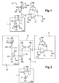
On a représenté schématiquement en relation avec la
Le pixel 1 (le terme « pixel » doit s'entendre par extension comme l'ensemble des structures disposées dans l'emprise d'un point élémentaire de détection) comporte un bolomètre actif 2, un transistor NMOS d'injection 3 et un interrupteur 4 reliant le pixel 1 à la colonne de lecture 5, représentée ici en pointillé. La structure de compensation 6, également dénommée d'ébasage, selon une autre terminologie du domaine technique considéré, comporte un bolomètre aveugle 7 relié à une alimentation VSK et un transistor PMOS d'injection 8. En mode de fonctionnement nominal, le PMOS fonctionne en régime saturé. Le courant IComp, qui circule dans la branche de compensation, est défini par l'expression : 
- Vcomp désigne la tension aux bornes du bolomètre de
compensation 7 ; - Rcomp désigne la résistance dudit bolomètre de compensation.
- Vcomp is the voltage across the
compensation bolometer 7; - Rcomp denotes the resistance of said compensation bolometer.
Le courant circulant dans la branche active, qui comporte le transistor NMOS d'injection 3 s'exprime par la relation : 
- Iac désigne le courant de la branche active ;
- Vac désigne la tension aux bornes du bolomètre actif 2 ;
- Rac désigne la résistance dudit bolomètre actif.
- Iac is the current of the active branch;
- Vac denotes the voltage across the
active bolometer 2 ; - Rac denotes the resistance of said active bolometer.
Les tensions de polarisation des transistors MOS d'injection sont choisies pour qu'en l'absence de flux de scène incident, c'est à dire par exemple lorsque l'on obture optiquement le système, la différence de courant di = Icomp-Iac entre la branche active et la branche aveugle de compensation soit sensiblement nulle.The polarization voltages of the injection MOS transistors are chosen so that in the absence of incident scene flux, that is to say for example when the system is optically shut off, the current difference di = I comp I ac between the active branch and the blind compensation branch is substantially zero.
Lorsque l'on souhaite lire un bolomètre actif, l'opération se déroule en deux phases. La première phase consiste à actionner l'interrupteur de remise à zéro « Reset » 9 court-circuitant la capacité d'intégration 10 de l'amplificateur opérationnel 11. On a alors : ![]()
![]()
La colonne de lecture en pointillé 5 est donc portée au potentiel VBUS. Ensuite on ouvre l'interrupteur « Reset » 9 et on ferme l'interrupteur de sélection « Select » 4 connectant le pixel 1 à la colonne de lecture 5. La différence de courant dI est alors intégrée sur une capacité Cint 10 durant un temps d'intégration fini Tint. L'intégration produit un niveau de sortie en tension de « Niveau Continu » ou NC, dans le cas de référence où l'on observe une scène à température uniforme, qui révèle typiquement les dispersions de la matrice d'imagerie. C'est le mode de caractérisation standard de lecture des bolomètres actifs. 
La polarisation des bolomètres est choisie de telle sorte à assurer à la fois une bonne dynamique du signal de sortie et une compensation efficace.The polarization of the bolometers is chosen so as to ensure both a good dynamic output signal and effective compensation.
Une expression plus rigoureuse serait obtenue en considérant pour le dernier terme l'intégrale sur Tint de la fonction dI(t), car les courants I ac et I comp ne sont pas constants. Cependant, pour la clarté de l'exposé, l'expression ci-dessus suffit à expliciter les paramètres à prendre en considération.A more rigorous expression would be obtained by considering for the last term the integral on Tint of the function dI (t), since the currents I ac and I comp are not constant. However, for the sake of clarity, the above expression suffices to explain the parameters to be taken into consideration.
Ce système de lecture présente certaines limitations liées à la reproduction du motif de compensation par colonne sur le circuit de lecture. En effet chaque colonne dispose d'un bolomètre de compensation et de son transistor PMOS d'injection. La reproduction imparfaite de ces différents éléments d'une colonne sur l'autre, inhérente aux dispersions spatiales intrinsèques des technologies de construction mises en oeuvre, engendre une dispersion dans l'efficacité de la compensation. Ces dispersions statistiques se traduisent par un courant de compensation non uniforme d'une colonne à l'autre, faisant apparaître des contrastes colonnaires visibles, affectant ainsi le signal disponible.This reading system has certain limitations related to the reproduction of the column compensation pattern on the read circuit. Indeed, each column has a compensation bolometer and its PMOS injection transistor. The imperfect reproduction of these different elements from one column to another, inherent to the intrinsic spatial dispersions of the construction technologies used, gives rise to a dispersion in the efficiency of the compensation. These dispersions Statistics result in a non-uniform compensation current from one column to the other, showing visible columnar contrasts, thus affecting the available signal.
La dispersion ΔRcomp sur la résistance Rcomp se traduit par une variation de courant de la forme : 
Le courant de compensation peut également s'exprimer en fonction de l'équation du courant dans le MOSFET d'injection selon l'expression suivante : 
- µp désigne la mobilité des porteurs positifs ;
- Cox désigne la capacité d'oxyde de grille ;
- Wp désigne la largeur du canal du PMOS ;
- Lp désigne la longueur du canal du PMOS ;
- VSGP désigne la tension de grille du PMOS ;
- VthP désigne la tension de seuil du PMOS.
- μ p denotes the mobility of positive carriers;
- C ox is the gate oxide capacity;
- W p is the width of the PMOS channel;
- L p is the length of the PMOS channel;
- V SGP refers to the gate voltage of the PMOS;
- V thP is the threshold voltage of the PMOS.
De nombreux paramètres peuvent varier dans cette équation, engendrant une non-uniformité colonnaire du courant de compensation. Naturellement, les paramètres lithographiques Wp et Lp d'une colonne sur l'autre impliquent des différences de courant. La fluctuation de longueur du canal constitue également l'une des causes possibles de cette non-uniformité. Il existe des techniques connues de l'homme du métier afin de limiter ces dispersions.Many parameters can vary in this equation, generating a columnar non-uniformity of the compensation current. Naturally, the lithographic parameters W p and L p from one column to the other imply current differences. Channel length fluctuation is also one of the possible causes of this non-uniformity. There are techniques known to those skilled in the art to limit these dispersions.
En revanche, la dispersion de tension de seuil VthP pose problème. Si on suppose une variation δVth de tension de seuil, la variation colonnaire de courant peut alors s'exprimer de la façon suivante : 
Outre ces dispersions statiques, le circuit représenté sur la 
- kB est la constante de Boltzmann ;
- KF désigne le coefficient de bruit en 1/f du matériau.
- k B is the Boltzmann constant;
- K F denotes the noise coefficient in 1 / f of the material.
La puissance de bruit apportée par la structure de compensation, telle qu'exprimée par la relation ci-dessus, augmente d'un incrément constant pour chaque décade de fréquence supplémentaire comprise entre les deux bornes d'intégration fmin et fmax. Or, les bolomètres de compensation sont polarisés en permanence, donc la borne inférieure de fréquence fmin de l'intégration peut donc être considérée très basse, dans la mesure où le composant reste sous tension sur une période prolongée, une fois le détecteur activé. Les perturbations par colonne (exprimées par l'homme du métier de manière analytique par la puissance de bruit ci-dessus) se manifestent comme un «offset» ou décalage, au premier ordre invariant d'une image sur l'autre, si l'on considère les fréquences inférieures à la fréquence trame, mais variable sur une période de temps plus étendue, lorsque la caméra intégrant un tel détecteur est en fonctionnement depuis plusieurs minutes.The noise power provided by the compensation structure, as expressed by the above relationship, increases by a constant increment for each additional decade of frequency between the two integration terminals f min and f max . However, the compensating bolometers are permanently polarized, so the lower limit of frequency f min of the integration can therefore be considered very low, insofar as the component remains energized for an extended period, once the detector is activated. The column perturbations (expressed by those skilled in the art analytically by the noise power above) are manifested as an "offset" or shift, at first order invariant from one image to the other, if the we consider frequencies lower than the frame frequency, but variable over a longer period of time, when the camera incorporating such a detector has been in operation for several minutes.
Outre cette limitation, la tendance du marché vers une augmentation du nombre de points des capteurs bolométriques, fait que les bolomètres de compensation de chaque colonne, efficaces sur de petits imageurs comme référence absolue de température, agissent comme des références « locales » de températures, du point de vue des bolomètres actifs les plus éloignés. Ainsi, si une source thermique d'origine quelconque, par exemple des éléments de circuiterie localement plus ou moins dissipatifs, peut influencer tout ou partie des bolomètres de compensation, ces derniers seront influencés en relation avec leur éloignement de la source de perturbation, et reproduisent ainsi une distribution de courant de compensation inadaptée aux dispersions de température du substrat vues par les bolomètres sensibles, non concernés, ou en général de manière différente, par ladite source thermique.In addition to this limitation, the market tendency towards an increase in the number of points of the bolometric sensors, makes that the compensation bolometers of each column, effective on small imagers as absolute reference of temperature, act like "local" references of temperatures, from the point of view of the most distant active bolometers. Thus, if a thermal source of any origin, for example locally more or less dissipative circuitry elements, can influence all or part of the compensation bolometers, the latter will be influenced in relation to their distance from the source of disturbance, and thus reproduce a compensation current distribution unsuited to the substrate temperature dispersions seen by the sensitive bolometers, not concerned, or in general in a different manner, by said thermal source.
La présente invention vise un dispositif de détection mettant en oeuvre une unique structure de compensation, et permettant de s'affranchir des limitations de qualité des images, notamment liées aux différences de contraste colonnaires et aux dispersions spatiales des structures électroniques élémentaires distribuées dans chaque colonne.The present invention aims a detection device implementing a single compensation structure, and to overcome the limitations of image quality, particularly related to differences in columnar contrast and spatial dispersions of elementary electronic structures distributed in each column.
Ce dispositif de détection infrarouge comprend les caractéristiques de la revendication 1.This infrared detection device comprises the features of
En d'autres termes, l'intégralité de la matrice de bolomètres est compensée par une structure unique, permettant ainsi d'éviter les contrastes colonnaires observables avec les détecteurs de l'état antérieur de la technique.In other words, the entire bolometer array is compensated by a single structure, thereby avoiding columnar contrasts observable with the detectors of the prior art.
Selon l'invention, les moyens de production du courant de référence comportent :
- une ligne d'alimentation connectée à l'une des bornes dudit bolomètre aveugle ;
- un transistor d'injection, connecté à l'autre borne dudit bolomètre aveugle, de manière à imposer le courant de référence via une tension appliquée sur sa grille ;
- un convertisseur courant - tension convertissant ledit courant de référence en une tension de référence.
- a power line connected to one of the terminals of said blind bolometer;
- an injection transistor, connected to the other terminal of said blind bolometer, so as to impose the reference current via a voltage applied to its gate;
- a current - voltage converter converting said reference current into a reference voltage.
Selon l'invention, le bolomètre aveugle peut être constitué d'un ou plusieurs bolomètres aveugles élémentaires connectés ensemble. Ce ou ces bolomètres aveugles sont réalisés de manière similaire aux bolomètres actifs, mais présentent une résistance thermique négligeable par rapport au substrat.According to the invention, the blind bolometer may consist of one or more elementary blind bolometers connected together. This or these blind bolometers are made similar to the active bolometers, but have negligible thermal resistance relative to the substrate.
Selon l'invention, les moyens de copie simultanée pour chaque colonne de la matrice dudit courant de référence sont constitués par des miroirs de courant disposés dans chacune desdites colonnes, lesdits miroirs comportant chacun un convertisseur tension - courant.According to the invention, the simultaneous copying means for each column of the matrix of said reference current are constituted by current mirrors disposed in each of said columns, said mirrors each comprising a voltage-current converter.
Selon l'invention, le miroir de courant mis en oeuvre dans chacune des colonnes est un miroir de courant différentiel.According to the invention, the current mirror used in each of the columns is a differential current mirror.
La manière de réaliser l'invention et les avantages qui en découlent ressortiront mieux des exemples de réalisation qui suivent, donnés à titre indicatif et non limitatif à l'appui des figures annexées.
- La
figure 1 déjà décrite est une représentation schématique du principe de lecture d'une matrice active de bolomètres. - La
figure 2 est une représentation schématique analogue de lafigure 1 , mais illustrant le principe général d'une unique structure de compensation. - La
figure 3 représente une vue analogue à lafigure 2 d'une forme de réalisation de l'invention, illustrant la source de courant et le miroir de courant différentiel de la structure de référence, et le miroir différentiel de la structure par colonne.
- The
figure 1 already described is a schematic representation of the principle of reading an active matrix of bolometers. - The
figure 2 is a similar schematic representation of thefigure 1 but illustrating the general principle of a single compensation structure. - The
figure 3 represents a view similar to thefigure 2 an embodiment of the invention, illustrating the current source and the differential current mirror of the reference structure, and the differential mirror of the column structure.
Dans la suite de la description, le même numéro de référence identifie des éléments identiques ou de même nature fonctionnelle lorsque cela peut s'appliquer.In the remainder of the description, the same reference number identifies elements that are identical or of the same functional nature when this may apply.
De manière générale, et ainsi que déjà précisé, la matrice de détecteurs bolométriques est formée sur un substrat en silicium, dans lequel est réalisé le circuit de lecture. Ce substrat est traditionnellement recouvert, au niveau des structures actives, c'est à dire à l'aplomb de la zone optiquement sensible, d'une couche métallique réfléchissante. Cette dernière est destinée, de manière connue, à former une cavité quart-d'onde entre le substrat et les parties absorbantes du détecteur.In general, and as already stated, the bolometric detector matrix is formed on a silicon substrate, in which the read circuit is formed. This substrate is traditionally covered, at the level of the active structures, ie directly above the optically sensitive zone, with a reflective metal layer. The latter is intended, in known manner, to form a quarter-wave cavity between the substrate and the absorbent parts of the detector.
Les zones optiquement actives sont formées d'un pavage de membranes suspendues, comportant au dessus du circuit de lecture, un matériau bolométrique. Ces membranes sont supportées au moyen de structures essentiellement verticales, conductrices de l'électricité. Ces structures, réalisées à l'aide d'un matériau métallique, sont destinées en outre à amener les potentiels d'excitation générés par le circuit de lecture vers les parties conductrices, également dénommées électrodes, de la membrane de chaque détecteur bolométrique élémentaire, via des structures allongées, également conductrices électriquement, mais résistantes thermiquement.The optically active zones are formed by a tiling of suspended membranes, comprising, above the reading circuit, a bolometric material. These membranes are supported by means of essentially vertical, electrically conductive structures. These structures, made using a metallic material, are further intended to bring the excitation potentials generated by the reading circuit to the conductive parts, also called electrodes, of the membrane of each elementary bolometric detector, via elongate structures, also electrically conductive, but thermally resistant.
Cette résistance thermique, dite aussi « isolation thermique », est destinée à permettre l'échauffement du bolomètre sous l'effet du rayonnement infra-rouge à détecter.This thermal resistance, also called "thermal insulation", is intended to allow the heating of the bolometer under the effect of infra-red radiation to be detected.
Le circuit de lecture applique de manière séquentielle un courant électrique qui traverse la structure suspendue. Ce courant circule à travers un matériau, dont la résistivité varie avec la température, qu'on appelle matériau bolomètrique. Les matériaux les plus répandus pour cet usage sont l'oxyde de vanadium (formule générique VOx) et le silicium amorphe (a-Si).The read circuit sequentially applies an electric current that passes through the suspended structure. This current flows through a material whose resistivity varies with temperature, which is called a bolometric material. The most common materials for this purpose are vanadium oxide (generic formula VO x ) and amorphous silicon (a-Si).
Cette matrice est pourvue d'une structure de compensation, destinée à dériver la majeure partie du courant électrique de mode commun traversant chacun des détecteurs bolométriques qui la constitue, et dont le principe est décrit en relation avec la
Cette structure de compensation est unique pour l'intégralité de la matrice.This compensation structure is unique for the entire matrix.
Selon un exemple de réalisation, cette structure unique de compensation 18 comporte un bolomètre de compensation 12, aveugle, et plus précisément insensible au rayonnement infrarouge, de résistance Rcomp, constitué par un seul ou plusieurs bolomètres élémentaires connectés ensemble. Une ligne d'alimentation électrique 13 (VSK) est connectée à l'une des bornes de ladite résistance Rcomp. L'autre borne de ladite résistance est connectée à un transistor d'injection 14, de telle sorte à imposer un courant de référence (Iref) à travers la résistance Rcomp du bolomètre de compensation 12 via une tension de grille (GSK) appliquée sur la grille dudit transistor. Ce faisant, le bolomètre aveugle 12 est constamment polarisé à l'aide du transistor d'injection 14 piloté par la tension de grille (GSK).According to an exemplary embodiment, this
Un convertisseur courant - tension 15 convertit le courant de référence (Iref) en une tension de référence (Vref).A current-
Ce courant de référence (Iref) est dupliqué pour chacune des colonnes au moyen d'un miroir de courant 16 disposé dans lesdites colonnes 5, comportant chacun un convertisseur tension (Vref) - courant (Iref).This reference current (I ref ) is duplicated for each of the columns by means of a
Les miroirs de courant sont bien connus de l'homme du métier, de sorte qu'il n'y a pas lieu de les décrire ici plus en détail. Il convient simplement de rappeler qu'un tel miroir de courant est un circuit particulier, en l'espèce constitué de transistors, permettant de refléter (dupliquer) le courant de référence (Iref) en un courant de sortie, idéalement égal, et en tout cas proportionnel au courant de référence, indépendamment de la charge connectée au courant de sortie, et en l'espèce à l'intégrateur décrit ci-après.Current mirrors are well known to those skilled in the art, so there is no need to describe them here in more detail. It is simply recalled that such a current mirror is a particular circuit, in this case consisting of transistors, to reflect (duplicate) the reference current (I ref ) into an output current, ideally equal, and any case proportional to the reference current, regardless of the load connected to the output current, and in this case to the integrator described below.
En effet, un intégrateur de courant 19, formé de l'amplificateur 11 et de la capacité 10, est associé à chacune des colonnes 5 de la matrice. Celui-ci est destiné à intégrer la différence entre le courant traversant le bolomètre actif 2 de la ligne en cours de lecture et le courant de référence (Iref), provenant du miroir de courant.Indeed, a
Le courant de référence (Iref) est donc copié selon un courant I 2 dans toutes les colonnes de la matrice à l'aide du miroir de courant 16. Chacune desdites colonnes dispose d'un miroir de courant supplémentaire 17 pour retourner le sens du courant I 2 vers un courant I3 de compensation, afin de rendre le courant de référence (Iref) compatible avec la structure d'intégration classiquement utilisée.The reference current (I ref ) is thus copied according to a current I 2 in all the columns of the matrix using the
II n'y a donc plus de bolomètres de compensation dans chacune des colonnes, mais un seul bolomètre de compensation pour toute la matrice.There is therefore no more compensation bolometers in each of the columns, but only one compensation bolometer for the entire matrix.
Il convient de souligner que le miroir de courant 17 n'est nécessaire que si le bolomètre actif 2 est référencé à la masse du détecteur, condition non nécessaire au fonctionnement de celui-ci. Ainsi, il est possible de référencer le bolomètre actif 2 à la tension VSK ou tout autre potentiel supérieur à V BUS afin de supprimer le miroir de courant 17 en connectant directement le transistor du miroir de courant 16 à la colonne 5. It should be emphasized that the
Avec le dispositif particulier de cet exemple, on s'affranchit des dispersions liées aux bolomètres de compensation distribués. Ainsi, on observe la suppression de l'une des sources de dispersion colonnaire, constituant l'un des inconvénients des matrices de détection de l'état antérieur de la technique.With the particular device of this example, it dispenses with dispersions related to compensated compensation bolometers. Thus, we observe the removal of one of the sources of columnar dispersion, constituting one of the drawbacks of the detection matrices of the prior art.
De plus, la suppression de tels bolomètres de compensation traditionnellement associés à chaque colonne permet de générer un gain de place conséquent en terme de surface de substrat consommée. Il est en effet rappelé que ces structures de compensation doivent présenter un niveau de bruit basse fréquence aussi modéré que possible pour ne pas nuire aux performances globales de l'imageur. Or, cet objectif exige le recours à un volume relativement élevé de matériau sensible pour l'élaboration de structures de compensation peu bruyantes, et donc corollairement, d'une surface conséquente, puisque les structures sont traditionnellement élaborées à partir de couches fines.In addition, the removal of such compensating bolometers traditionally associated with each column makes it possible to generate a considerable space saving in terms of consumed substrate area. It is recalled that these compensation structures must have a low frequency noise level as moderate as possible so as not to harm the overall performance of the imager. However, this objective requires the use of a relatively high volume of sensitive material for the development of low noise compensation structures, and therefore corollary, a consistent surface, since the structures are traditionally developed from thin layers.
La forme de réalisation telle qu'illustrée au sein de la
Afin de surmonter ces limitations, l'invention propose, dans le cadre d'une forme de réalisation de l'invention illustrée au sein de la
Dans ce cadre, deux transistors proches peuvent être appariés grâce aux techniques de dessin connues et à un dimensionnement judicieux des transistors.In this context, two nearby transistors can be matched using known drawing techniques and judicious sizing of the transistors.
En l'espèce, la structure de compensation de référence 18 est conservée. Elle constitue la source de courant de référence il = Iref. Elle est associée à un convertisseur courant - tension différentielle 22, comportant de manière connue, au moins un miroir de courant et des générateurs de courant.In this case, the
Plus précisément, ce convertisseur comprend :
- ■ une source de courant de
mode commun Icom 24 ; - ■ un additionneur de
courant 25 assurant l'opération Icom + Iref/2 ; - ■ un soustracteur de
courant 26 assurant l'opération Icom - Iref/2.
- ■ an
Icom 24 common mode power source ; - A
current adder 25 providing the Icom + Iref / 2 operation; - A
current subtracter 26 providing the Icom-Iref / 2 operation.
Ce convertisseur assure alors la conversion courant - tension, de telle sorte à définir respectivement :
- ■ une tension de référence Vcmd+ correspondant au courant Icom + Iref/2 ;
- ■ une tension de référence Vcmd- correspondant au courant Icom - Iref/2 ;
- A reference voltage V cmd + corresponding to the current Icom + Iref / 2;
- A reference voltage V cmd corresponding to the current Icom-Iref / 2;
Il est donc constitué une structure unique et commune à tout le détecteur, et identifiée par la référence 20. It is thus constituted a single structure and common to all the detector, and identified by the
Chacune des colonnes comporte un convertisseur tension - courant 23, comportant chacun :
- ■ deux convertisseurs tension -
courant - ■ un soustracteur de
courant 29 assurant l'opération I1 - I2.
- Two voltage-
current converters - A
current subtracter 29 performing the operation I 1 - I 2 .
Les détails de construction et les avantages inhérents aux miroirs de courant différentiels sont bien connus de l'homme du métier, de sorte qu'il n'y a pas lieu de les détailler davantage dans le cadre de la présente invention.The construction details and advantages inherent in differential current mirrors are well known to those skilled in the art, so there is no need to further detail them in the context of the present invention.
Le courant issu de ce convertisseur tension - courant 23 est dupliqué pour chacune des colonnes au moyen du miroir de courant 16 disposé également dans chacune desdites colonnes 5. Ce faisant, le courant de référence (Iref) est copié selon un courant il dans toutes les colonnes de la matrice à l'aide du miroir de courant 16. Chacune desdites colonnes dispose d'un miroir de courant supplémentaire 17 pour retourner le sens du courant il vers un courant de compensation, afin de rendre le courant de référence (Iref) compatible avec la structure d'intégration 19 précédemment décrite.The current from this voltage-
On constate que dans le cadre de cette forme particulière de réalisation, les transistors entrant dans la constitution de la structure unique de compensation 20 sont très proches les uns des autres, et peuvent donc facilement être appariés. De même, les transistors 27 et 28 sont disposés dans chaque colonne, et peuvent donc également être appariés. En revanche, ces derniers ne peuvent être appariés aux transistors de la structure 20. Le fait de travailler non pas avec une tension Vref unique, mais avec une double tension Vcmd+/Vcmd- différentielle, permet de limiter substantiellement l'influence de dispersions spatiales des structures électroniques élémentaires (MOS) distribuées dans chaque colonne, en particulier en termes de dispersion de tension de seuil. Ce faisant, on gagne en précision par rapport à la forme de réalisation de la
Quel que soit le mode de réalisation retenu, on supprime le bolomètre de compensation de chaque colonne. Ce faisant, on supprime également le bruit en 1/f qu'il génère dans les structures classiques de détection, telles qu'illustrées en relation avec la
Certes, le bruit en 1/f est toujours présent lors du fonctionnement du bolomètre unique de compensation mis en oeuvre dans l'invention, mais d'une part ce bruit peut aisément être réduit à quantité négligeable par la mise en oeuvre d'un volume de matériau bolométrique suffisamment élevé, au prix d'une surface de substrat consommée très réduite par rapport à la surface totale de l'imageur.Admittedly, the noise in 1 / f is always present during the operation of the single compensation bolometer implemented in the invention, but on the one hand this noise can easily be reduced to a negligible amount by the implementation of a volume of bolometric material sufficiently high, at the cost of a consumed substrate surface very small compared to the total surface of the imager.
En outre, cette surface consommée demeure de toutes façons tout à fait négligeable au regard de ce qu'exige la construction des structures bolométriques de compensation disposées dans chaque colonne dans les structures de l'état antérieur de la technique de la
Au surplus, son effet s'applique à tous les pixels de la matrice et non plus de manière décorrellée entre colonnes, l'effet résiduel éventuel étant beaucoup moins préjudiciable.Moreover, its effect applies to all the pixels of the matrix and no longer in a decorrelated manner between columns, the possible residual effect being much less detrimental.
Enfin, le bruit en 1/f ramené par les miroirs de courant, peut être minimisé à l'aide de techniques connues de l'homme du métier.Finally, the noise in 1 / f brought back by the current mirrors, can be minimized using techniques known to those skilled in the art.
Ainsi, l'invention trouve tout particulièrement application dans le domaine des capteurs d'image à détection bolométrique, quelle que soit la bande optique de détection et le type de capteur bolométrique mis en oeuvre (notamment mais non limitativement à base de silicium amorphe (a-Si), d'oxydes de vanadium (Vox), de métaux (Ti)).Thus, the invention is particularly applicable in the field of image sensors with bolometric detection, whatever the optical detection band and the type of bolometric sensor used (in particular but not limited to amorphous silicon (a). -Si), vanadium oxides (Vox), metals (Ti)).
En outre, en raison de sa capacité d'adaptation à différentes températures de fonctionnement, l'invention s'applique aussi bien aux capteurs régulés thermiquement qu'aux capteurs opérant à température de plan focal variable.In addition, because of its ability to adapt to different operating temperatures, the invention applies both to thermally controlled sensors and sensors operating at variable focal plane temperature.
De plus, la capacité intrinsèque de faible bruit basse-fréquence en colonne permet d'intégrer les détecteurs réalisés selon l'invention dans des caméras qui seraient dépourvues d'obturateur (ou selon l'expression anglo-saxonne « shutter »).In addition, the intrinsic low-frequency low-noise column-based capability makes it possible to integrate the detectors made according to the invention into cameras that would be shutter-free (or, in the English expression, "shutter ").
Mais bien entendu, l'invention reste parfaitement compatible avec les caméras traditionnelles munies d'un tel obturateur. Ce faisant, on aboutit à une diminution sensible du coût de fabrication de telles caméras, ainsi qu'à une simplification de leur mise en oeuvre par l'utilisateur.But of course, the invention remains perfectly compatible with traditional cameras provided with such a shutter. In doing so, it leads to a significant decrease in the cost of manufacturing such cameras, and a simplification of their implementation by the user.
Claims (3)
- A device for detecting infrared radiation comprising :• an array of bolometric detectors which are sensitive to the incident radiation and are referred to as "active" (2) formed above a substrate ;• a read circuit produced for sequentially addressing each of the columns of detectors of said array, said circuit being formed in said substrate and comprising :characterized in that the means for producing a reference current for each column of the array of active bolometers comprise :- for each column of said array, means (16, 17, 18 ; 18, 20, 21) for producing a reference current (Iref) ;- for each column of said array, an integrator (19) designed to integrate the difference between the current flowing through the active bolometer of the column the reference current ; and- means for ordering :■ the selection of one row of active bolometers of the array ;■ the simultaneous biasing of the active bolometers of the selected row ;■ the simultaneous production of reference currents (Iref) for the columns of the array;■ the simultaneous integration of the differences between the currents flowing through the active bolometers of the selected row and the reference currents (Iref) ;• means (18) for producing a unique reference current (Iref) for all the columns of the array of active bolometers from a unique bolometer which is insensitive to the radiation and referred to as "blind" (12), formed above the substrate ;• means (17, 18 ; 18, 20, 21) of simultaneously copying for each column of the array said reference current (Iref) consisting of current mirrors (16) located in each of said columns, said mirrors each comprising a voltage-to-current converter, the current mirror implemented in each column being a differential current mirror.
- A device for detecting infrared radiation as claimed in claim 1, characterized in that the means of producing the reference current (Iref) comprise:• a power supply line (13) connected to one of the terminals of said blind bolometer (12);• a charge injection transistor (14) connected to the other terminal of said blind bolometer (12) so as to impose the reference current (Iref) through a voltage applied to its gate;• a current-to-voltage converter (15) which converts said reference current (Iref) to a reference voltage.
- A device for detecting electromagnetic radiation as claimed in any of claims 1 and 2, characterized in that the blind bolometer (12) consists of one or more elementary blind bolometers connected to each other.
Applications Claiming Priority (1)
| Application Number | Priority Date | Filing Date | Title |
|---|---|---|---|
| FR0756214A FR2918449B1 (en) | 2007-07-02 | 2007-07-02 | DEVICE FOR DETECTING INFRARED RADIATION WITH BOLOMETRIC DETECTORS |
Publications (2)
| Publication Number | Publication Date |
|---|---|
| EP2012100A1 EP2012100A1 (en) | 2009-01-07 |
| EP2012100B1 true EP2012100B1 (en) | 2012-11-14 |
Family
ID=39030895
Family Applications (1)
| Application Number | Title | Priority Date | Filing Date |
|---|---|---|---|
| EP08300224A Active EP2012100B1 (en) | 2007-07-02 | 2008-06-17 | Device for detecting infrared radiation using bolometric detectors |
Country Status (6)
| Country | Link |
|---|---|
| US (1) | US7928387B2 (en) |
| EP (1) | EP2012100B1 (en) |
| CN (1) | CN101339074B (en) |
| CA (1) | CA2632505C (en) |
| FR (1) | FR2918449B1 (en) |
| RU (1) | RU2454752C2 (en) |
Families Citing this family (18)
| Publication number | Priority date | Publication date | Assignee | Title |
|---|---|---|---|---|
| IL167637A (en) * | 2005-03-24 | 2009-09-22 | Semi Conductor Devices An Elbi | Method and system for determining the rate of non uniformity of bolometer based systems |
| IL167641A (en) * | 2005-03-24 | 2011-07-31 | Semi Conductor Devices An Elbit Systems Rafael Partnership | System for measuring and compensating for the case temperature variations in a bolometer based system |
| US8124937B2 (en) | 2009-01-15 | 2012-02-28 | Raytheon Company | System and method for athermal operation of a focal plane array |
| FR2944870B1 (en) * | 2009-04-23 | 2011-06-24 | Commissariat Energie Atomique | BOLOMETER SENSOR HAVING MEANS FOR ELECTRICALLY REGULATING THE EFFECTS OF TEMPERATURE |
| EP2589939B1 (en) * | 2010-07-01 | 2020-03-18 | Panasonic Intellectual Property Management Co., Ltd. | Object detection device for objects in a target space |
| FR2963850B1 (en) * | 2010-08-10 | 2012-09-07 | Soc Fr Detecteurs Infrarouges Sofradir | DETECTION DEVICE WITH IMPROVED POLARIZATION CONDITIONS |
| JP5331091B2 (en) * | 2010-11-18 | 2013-10-30 | パナソニック株式会社 | COMMUNICATION SYSTEM, TRANSMISSION DEVICE, RECEPTION DEVICE, AND COMMUNICATION METHOD |
| FR2969763B1 (en) * | 2010-12-22 | 2013-02-15 | Commissariat Energie Atomique | MEASURING SYSTEM AND IMAGER HAVING SUCH A SYSTEM |
| US8610062B2 (en) | 2011-03-24 | 2013-12-17 | Raytheon Company | Apparatus and method for multi-spectral imaging |
| CN102494781B (en) * | 2011-12-14 | 2013-04-10 | 电子科技大学 | Readout circuit bias structure |
| CN108401497B (en) * | 2018-02-27 | 2020-11-13 | 深圳市汇顶科技股份有限公司 | Image sensor and output compensation circuit of image sensor |
| FR3088512B1 (en) * | 2018-11-09 | 2020-10-30 | Schneider Electric Ind Sas | PROCESS FOR PROCESSING AN IMAGE |
| CN109459141A (en) * | 2018-12-18 | 2019-03-12 | 山西德润翔电力科技有限公司 | Double color infrared ray device |
| CN110296761B (en) * | 2019-07-25 | 2020-06-05 | 北京安酷智芯科技有限公司 | Reading circuit |
| US10827090B1 (en) * | 2019-09-16 | 2020-11-03 | Innolux Corporation | Electronic device and method for operating electronic device |
| CN111579095B (en) * | 2020-04-30 | 2021-11-30 | 南京雷石电子科技有限公司 | Vehicle-mounted low-temperature infrared detection system |
| IL275896B (en) * | 2020-07-07 | 2022-07-01 | Frank Amit | Imaging apparatus and method |
| CN112082661B (en) * | 2020-07-27 | 2021-09-14 | 上海集成电路研发中心有限公司 | Infrared detector structure based on pixel combination and combination method thereof |
Family Cites Families (24)
| Publication number | Priority date | Publication date | Assignee | Title |
|---|---|---|---|---|
| GB9404111D0 (en) * | 1994-03-03 | 1994-04-20 | Philips Electronics Uk Ltd | A charge storage device |
| US5784178A (en) * | 1996-03-06 | 1998-07-21 | Dyna Image Corporation | High performance contact image sensor |
| US6141048A (en) * | 1996-08-19 | 2000-10-31 | Eastman Kodak Company | Compact image capture device |
| JPH10122957A (en) * | 1996-10-22 | 1998-05-15 | Nikon Corp | Thermal infrared image sensor |
| US6518962B2 (en) * | 1997-03-12 | 2003-02-11 | Seiko Epson Corporation | Pixel circuit display apparatus and electronic apparatus equipped with current driving type light-emitting device |
| US6396045B1 (en) * | 1997-09-26 | 2002-05-28 | Qinetiq Limited | Sensor apparatus |
| US6384413B1 (en) * | 1998-10-13 | 2002-05-07 | California Institute Of Technology | Focal plane infrared readout circuit |
| FR2788129B1 (en) * | 1998-12-30 | 2001-02-16 | Commissariat Energie Atomique | BOLOMETRIC DETECTOR WITH ANTENNA |
| US6704050B1 (en) * | 1999-04-23 | 2004-03-09 | Polaroid Corporation | Active-pixel image sensing device with linear mode voltage to current conversion |
| US6583416B1 (en) * | 1999-11-15 | 2003-06-24 | Sarnoff Corporation | Uncooled IR detector array having improved temperature stability and reduced fixed pattern noise |
| JP2001245215A (en) * | 2000-01-11 | 2001-09-07 | Agilent Technol Inc | Improved active pixel sensor having reference signal |
| JP3866069B2 (en) * | 2001-09-26 | 2007-01-10 | 株式会社東芝 | Infrared solid-state imaging device |
| US6812465B2 (en) * | 2002-02-27 | 2004-11-02 | Indigo Systems Corporation | Microbolometer focal plane array methods and circuitry |
| KR101065825B1 (en) * | 2003-04-25 | 2011-09-20 | 티피오 디스플레이스 코포레이션 | Method and device for driving an active matrix display panel |
| US7119334B2 (en) * | 2003-11-03 | 2006-10-10 | Namal Technologies Ltd. | Thermal imaging system and method |
| FR2862160B1 (en) * | 2003-11-10 | 2006-05-12 | Ulis | DEVICE FOR DETECTING INFRARED RADIATION WITH BOLOMETRIC DETECTORS |
| US20060007206A1 (en) * | 2004-06-29 | 2006-01-12 | Damoder Reddy | Device and method for operating a self-calibrating emissive pixel |
| US7616231B2 (en) * | 2005-01-06 | 2009-11-10 | Goodrich Corporation | CMOS active pixel sensor with improved dynamic range and method of operation for object motion detection |
| GB0500111D0 (en) * | 2005-01-06 | 2005-02-09 | Koninkl Philips Electronics Nv | Inkjet print head |
| JP2006292594A (en) * | 2005-04-12 | 2006-10-26 | Nec Electronics Corp | Infrared detector |
| WO2007015235A1 (en) * | 2005-08-04 | 2007-02-08 | Semi-Conductor Devices-An Elbit Systems-Rafael Partnership | Circuitry for balancing a differential type focal plane array of bolometer based infra-red detectors |
| JP4654857B2 (en) * | 2005-09-26 | 2011-03-23 | ソニー株式会社 | DA converter, AD converter, semiconductor device |
| US7435961B2 (en) * | 2006-03-17 | 2008-10-14 | Lucent Technologies Inc. | Imaging sensor |
| JP4901320B2 (en) * | 2006-06-13 | 2012-03-21 | 三菱電機株式会社 | 2-wavelength image sensor |
-
2007
- 2007-07-02 FR FR0756214A patent/FR2918449B1/en not_active Expired - Fee Related
-
2008
- 2008-05-28 US US12/127,976 patent/US7928387B2/en not_active Expired - Fee Related
- 2008-05-29 CA CA2632505A patent/CA2632505C/en active Active
- 2008-06-09 RU RU2008123479/28A patent/RU2454752C2/en active
- 2008-06-10 CN CN2008101110592A patent/CN101339074B/en active Active
- 2008-06-17 EP EP08300224A patent/EP2012100B1/en active Active
Also Published As
| Publication number | Publication date |
|---|---|
| EP2012100A1 (en) | 2009-01-07 |
| FR2918449A1 (en) | 2009-01-09 |
| CN101339074B (en) | 2011-12-28 |
| RU2454752C2 (en) | 2012-06-27 |
| CA2632505A1 (en) | 2009-01-02 |
| RU2008123479A (en) | 2009-12-20 |
| US7928387B2 (en) | 2011-04-19 |
| US20090008555A1 (en) | 2009-01-08 |
| FR2918449B1 (en) | 2010-05-21 |
| CA2632505C (en) | 2016-09-13 |
| CN101339074A (en) | 2009-01-07 |
Similar Documents
| Publication | Publication Date | Title |
|---|---|---|
| EP2012100B1 (en) | Device for detecting infrared radiation using bolometric detectors | |
| EP2012101B1 (en) | Device for detecting electromagnetic radiation, in particular infrared | |
| CA2647365C (en) | Electromagnetic detection device including a resistive imaging bolometer, system including a matrix of such bolometers, and process for reading an imaging bolometer in such a system | |
| EP2071309B1 (en) | Device for detecting infrared radiation comprising an imaging resistive bolometer, system comprising an array of such bolometers and method of reading an imaging bolometer integrated in such a system | |
| EP2770312B1 (en) | Bolometric detector having a temperature dependent controlled polarisation | |
| EP2208976B1 (en) | Device for detecting electromagnetic radiation | |
| EP2163871A1 (en) | Device for detecting infrared radiation using a bolometer and method for reading out such a bolometer integrated into a bolometer array | |
| EP3140906B1 (en) | High dynamic range device for integrating an electrical current | |
| EP2425220A1 (en) | System and method for detecting infrared radiation | |
| FR2875336A1 (en) | DEVICE FOR DETECTING INFRARED RADIATION WITH BOLOMETRIC DETECTORS | |
| EP2209305B1 (en) | Device for detecting electromagnetic radiation | |
| EP0354106B1 (en) | Noise eliminating circuit integrated in a solid-state imager | |
| EP2037241A1 (en) | Device for detecting electromagnetic radiation with current limit | |
| CA2452627A1 (en) | Electromagnetic radiation detection device | |
| FR2943415A1 (en) | METHOD FOR ADJUSTING A RADIATION DETECTION CIRCUIT | |
| FR2942074A1 (en) | Electromagnetic radiation i.e. infrared radiation, detecting device for use in thermal imagery field, has logical block determining state of switch during integration time by cumulated sequential addition of capacities of two capacitors | |
| EP4025886A1 (en) | Infrared sensor able to capture instantaneously |
Legal Events
| Date | Code | Title | Description |
|---|---|---|---|
| PUAI | Public reference made under article 153(3) epc to a published international application that has entered the european phase |
Free format text: ORIGINAL CODE: 0009012 |
|
| AK | Designated contracting states |
Kind code of ref document: A1 Designated state(s): AT BE BG CH CY CZ DE DK EE ES FI FR GB GR HR HU IE IS IT LI LT LU LV MC MT NL NO PL PT RO SE SI SK TR |
|
| AX | Request for extension of the european patent |
Extension state: AL BA MK RS |
|
| 17P | Request for examination filed |
Effective date: 20090126 |
|
| 17Q | First examination report despatched |
Effective date: 20090225 |
|
| AKX | Designation fees paid |
Designated state(s): DE FR GB IT SE |
|
| GRAP | Despatch of communication of intention to grant a patent |
Free format text: ORIGINAL CODE: EPIDOSNIGR1 |
|
| RIC1 | Information provided on ipc code assigned before grant |
Ipc: H04N 5/335 20110101ALI20120807BHEP Ipc: G01J 5/22 20060101AFI20120807BHEP Ipc: H04N 5/33 20060101ALI20120807BHEP |
|
| GRAS | Grant fee paid |
Free format text: ORIGINAL CODE: EPIDOSNIGR3 |
|
| GRAA | (expected) grant |
Free format text: ORIGINAL CODE: 0009210 |
|
| AK | Designated contracting states |
Kind code of ref document: B1 Designated state(s): DE FR GB IT SE |
|
| REG | Reference to a national code |
Ref country code: GB Ref legal event code: FG4D Free format text: NOT ENGLISH |
|
| REG | Reference to a national code |
Ref country code: SE Ref legal event code: TRGR |
|
| REG | Reference to a national code |
Ref country code: DE Ref legal event code: R096 Ref document number: 602008020083 Country of ref document: DE Effective date: 20130110 |
|
| PLBE | No opposition filed within time limit |
Free format text: ORIGINAL CODE: 0009261 |
|
| STAA | Information on the status of an ep patent application or granted ep patent |
Free format text: STATUS: NO OPPOSITION FILED WITHIN TIME LIMIT |
|
| 26N | No opposition filed |
Effective date: 20130815 |
|
| REG | Reference to a national code |
Ref country code: DE Ref legal event code: R097 Ref document number: 602008020083 Country of ref document: DE Effective date: 20130815 |
|
| PGFP | Annual fee paid to national office [announced via postgrant information from national office to epo] |
Ref country code: IT Payment date: 20140619 Year of fee payment: 7 |
|
| PG25 | Lapsed in a contracting state [announced via postgrant information from national office to epo] |
Ref country code: IT Free format text: LAPSE BECAUSE OF NON-PAYMENT OF DUE FEES Effective date: 20150617 |
|
| REG | Reference to a national code |
Ref country code: FR Ref legal event code: PLFP Year of fee payment: 9 |
|
| REG | Reference to a national code |
Ref country code: FR Ref legal event code: PLFP Year of fee payment: 10 |
|
| REG | Reference to a national code |
Ref country code: FR Ref legal event code: PLFP Year of fee payment: 11 |
|
| PGFP | Annual fee paid to national office [announced via postgrant information from national office to epo] |
Ref country code: SE Payment date: 20220623 Year of fee payment: 15 Ref country code: GB Payment date: 20220616 Year of fee payment: 15 Ref country code: DE Payment date: 20220607 Year of fee payment: 15 |
|
| PGFP | Annual fee paid to national office [announced via postgrant information from national office to epo] |
Ref country code: FR Payment date: 20220628 Year of fee payment: 15 |
|
| REG | Reference to a national code |
Ref country code: DE Ref legal event code: R119 Ref document number: 602008020083 Country of ref document: DE |
|
| REG | Reference to a national code |
Ref country code: SE Ref legal event code: EUG |
|
| GBPC | Gb: european patent ceased through non-payment of renewal fee |
Effective date: 20230617 |