EP2006911B1 - Wiring substrate - Google Patents
Wiring substrate Download PDFInfo
- Publication number
- EP2006911B1 EP2006911B1 EP08158268A EP08158268A EP2006911B1 EP 2006911 B1 EP2006911 B1 EP 2006911B1 EP 08158268 A EP08158268 A EP 08158268A EP 08158268 A EP08158268 A EP 08158268A EP 2006911 B1 EP2006911 B1 EP 2006911B1
- Authority
- EP
- European Patent Office
- Prior art keywords
- insulating film
- wiring pattern
- film
- wiring
- substrate
- Prior art date
- Legal status (The legal status is an assumption and is not a legal conclusion. Google has not performed a legal analysis and makes no representation as to the accuracy of the status listed.)
- Expired - Fee Related
Links
- 239000000758 substrate Substances 0.000 title claims description 211
- 239000004065 semiconductor Substances 0.000 claims description 84
- 238000000034 method Methods 0.000 claims description 45
- 238000004519 manufacturing process Methods 0.000 claims description 23
- 238000005530 etching Methods 0.000 claims description 9
- 230000008878 coupling Effects 0.000 claims 2
- 238000010168 coupling process Methods 0.000 claims 2
- 238000005859 coupling reaction Methods 0.000 claims 2
- XUIMIQQOPSSXEZ-UHFFFAOYSA-N Silicon Chemical compound [Si] XUIMIQQOPSSXEZ-UHFFFAOYSA-N 0.000 description 24
- 229910052710 silicon Inorganic materials 0.000 description 24
- 239000010703 silicon Substances 0.000 description 24
- 238000007747 plating Methods 0.000 description 22
- 230000005540 biological transmission Effects 0.000 description 9
- 239000000463 material Substances 0.000 description 9
- 230000001590 oxidative effect Effects 0.000 description 6
- 239000000470 constituent Substances 0.000 description 3
- 238000009713 electroplating Methods 0.000 description 3
- 238000000151 deposition Methods 0.000 description 2
- 239000011347 resin Substances 0.000 description 2
- 229920005989 resin Polymers 0.000 description 2
- 239000000654 additive Substances 0.000 description 1
- 230000003247 decreasing effect Effects 0.000 description 1
- 230000002040 relaxant effect Effects 0.000 description 1
- 229910000679 solder Inorganic materials 0.000 description 1
Images


Classifications
-
- H—ELECTRICITY
- H01—ELECTRIC ELEMENTS
- H01L—SEMICONDUCTOR DEVICES NOT COVERED BY CLASS H10
- H01L23/00—Details of semiconductor or other solid state devices
- H01L23/12—Mountings, e.g. non-detachable insulating substrates
- H01L23/14—Mountings, e.g. non-detachable insulating substrates characterised by the material or its electrical properties
- H01L23/147—Semiconductor insulating substrates
-
- H—ELECTRICITY
- H01—ELECTRIC ELEMENTS
- H01L—SEMICONDUCTOR DEVICES NOT COVERED BY CLASS H10
- H01L23/00—Details of semiconductor or other solid state devices
- H01L23/48—Arrangements for conducting electric current to or from the solid state body in operation, e.g. leads, terminal arrangements ; Selection of materials therefor
- H01L23/488—Arrangements for conducting electric current to or from the solid state body in operation, e.g. leads, terminal arrangements ; Selection of materials therefor consisting of soldered or bonded constructions
- H01L23/498—Leads, i.e. metallisations or lead-frames on insulating substrates, e.g. chip carriers
- H01L23/49827—Via connections through the substrates, e.g. pins going through the substrate, coaxial cables
-
- H—ELECTRICITY
- H01—ELECTRIC ELEMENTS
- H01L—SEMICONDUCTOR DEVICES NOT COVERED BY CLASS H10
- H01L2224/00—Indexing scheme for arrangements for connecting or disconnecting semiconductor or solid-state bodies and methods related thereto as covered by H01L24/00
- H01L2224/01—Means for bonding being attached to, or being formed on, the surface to be connected, e.g. chip-to-package, die-attach, "first-level" interconnects; Manufacturing methods related thereto
- H01L2224/10—Bump connectors; Manufacturing methods related thereto
- H01L2224/15—Structure, shape, material or disposition of the bump connectors after the connecting process
- H01L2224/16—Structure, shape, material or disposition of the bump connectors after the connecting process of an individual bump connector
- H01L2224/161—Disposition
- H01L2224/16151—Disposition the bump connector connecting between a semiconductor or solid-state body and an item not being a semiconductor or solid-state body, e.g. chip-to-substrate, chip-to-passive
- H01L2224/16221—Disposition the bump connector connecting between a semiconductor or solid-state body and an item not being a semiconductor or solid-state body, e.g. chip-to-substrate, chip-to-passive the body and the item being stacked
- H01L2224/16225—Disposition the bump connector connecting between a semiconductor or solid-state body and an item not being a semiconductor or solid-state body, e.g. chip-to-substrate, chip-to-passive the body and the item being stacked the item being non-metallic, e.g. insulating substrate with or without metallisation
- H01L2224/16227—Disposition the bump connector connecting between a semiconductor or solid-state body and an item not being a semiconductor or solid-state body, e.g. chip-to-substrate, chip-to-passive the body and the item being stacked the item being non-metallic, e.g. insulating substrate with or without metallisation the bump connector connecting to a bond pad of the item
-
- H—ELECTRICITY
- H01—ELECTRIC ELEMENTS
- H01L—SEMICONDUCTOR DEVICES NOT COVERED BY CLASS H10
- H01L2924/00—Indexing scheme for arrangements or methods for connecting or disconnecting semiconductor or solid-state bodies as covered by H01L24/00
- H01L2924/15—Details of package parts other than the semiconductor or other solid state devices to be connected
- H01L2924/151—Die mounting substrate
- H01L2924/153—Connection portion
- H01L2924/1531—Connection portion the connection portion being formed only on the surface of the substrate opposite to the die mounting surface
- H01L2924/15311—Connection portion the connection portion being formed only on the surface of the substrate opposite to the die mounting surface being a ball array, e.g. BGA
Definitions
- the present disclosure relates to a wiring substrate, more particulary to a wiring substrate including an insulating film, e.g. for covering an upper surface and a lower surface of a semiconductor substrate, a first wiring pattern disposed on an upper surface side of the semiconductor substrate and preferably coupled to a through electrode and an electronic component, and a second wiring pattern disposed on a lower surface side of the semiconductor substrate and coupled to the through electrode and a mounting substrate.
- an insulating film e.g. for covering an upper surface and a lower surface of a semiconductor substrate
- a first wiring pattern disposed on an upper surface side of the semiconductor substrate and preferably coupled to a through electrode and an electronic component
- a second wiring pattern disposed on a lower surface side of the semiconductor substrate and coupled to the through electrode and a mounting substrate.
- a wiring substrate 200 shown in FIG.1 is used as the wiring substrate (interposer) for connecting electrically the semiconductor chip and the mounting substrate such as the motherboard.
- Such a wiring substrate is described in document EP 1 612 860 .
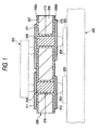
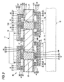
- FIG.1 is a sectional view of a wiring substrate in the related art.
- the wiring substrate 200 includes a semiconductor substrate 206 as a base material, an insulating film 207, through electrodes 208, and first and second wirings 211, 212.
- the semiconductor substrate 206 is a substrate shaped like a plate, and has through holes 215.
- a silicon substrate can be used as the semiconductor substrate 206.
- the insulating film 207 is formed to cover an upper surface 206A and a lower surface 206B of the semiconductor substrate 206 and surfaces of the semiconductor substrate 206, which are exposed from the through holes 215.
- a dielectric constant of the insulating film 207 is larger than a dielectric constant 1.0 of the air and is about 3.8.
- the through electrodes 208 are provided in the through holes 215 on which the insulating film 207 is formed.
- the through electrodes 208 are used to connect electrically the first wiring 211 and the second wiring 212.
- As the material of the through electrodes 208 for example, Cu can be used.
- the first wiring 211 is provided to extend over the insulating film 207 that is formed from upper end portions of the through electrodes 208 to the upper surface 206A of the semiconductor substrate 206.
- the first wiring 211 is a wiring to which an electronic component 201 is connected (mounted).
- the electronic component 201 the semiconductor chip whose base material is formed of the silicon substrate can be used.
- the second wiring 212 is provided to extend over the lower surface of the insulating film 207 that is formed from lower end portions of the through electrodes 208 to the lower surface 206B of the semiconductor substrate 206.
- the second wiring 212 is a wiring that is connected electrically to pads 203 of a mounting substrate 202 (concretely, the mother board, for example).
- a resin can be used as the material of the base member of the mounting substrate 202 (see e.g., JP-A-2007-42741 ).
- the first and second wirings 211, 212 contact the insulating film 207. Therefore, there is a problem that a transmission speed of a signal transmitted between the electronic component 201 connected to the first wiring 211 and the mounting substrate 202 connected electrically to the second wiring 212 cannot be increased.
- a material of the base member (concretely, silicon) of the wiring substrate 200 is different from that of the base member (concretely, resin) of the mounting substrate 202. Therefore, there is a problem that reliability of electrical connection between the wiring substrate 200 and the mounting substrate 202 is decreased on account of a difference of coefficient of thermal expansion between the wiring substrate 200 and the mounting substrate 202.
- Exemplary embodiments of the present invention address the above disadvantages and other disadvantages not described above.
- the present invention is not required to overcome the disadvantages described above, and thus, an exemplary embodiment of the present invention may not overcome any of the problems described above.
- a wiring substrate according to claim 1, a semiconductor device according to claim 9, and a method according to claim 11 is provided.
- a wiring substrate includes: a semiconductor substrate having a through hole; an insulating film provided to cover an upper surface, a lower surface and a first surface of the semiconductor substrate, the first surface corresponding to a side surface of the through hole; a through electrode provided in the through hole; a first wiring pattern disposed on an upper surface side of the semiconductor substrate and coupled to the through electrode; and a second wiring pattern disposed on a lower surface side of the semiconductor substrate and coupled to the through electrode.
- a first air gap is provided between the first wiring pattern and the insulating film formed on the upper surface, and a second air gap is provided between the second wiring pattern and the insulating film formed on the lower surface.
- a semiconductor device including the wiring substrate, and an electronic component coupled to the first wiring pattern.
- the method includes: i) preparing a semiconductor substrate; ii) forming a through hole in the semiconductor substrate; iii) forming an insulating film on an upper surface, a lower surface and a first surface of the semiconductor substrate, the first surface corresponding to a side surface of the through hole; iv) providing a through electrode in the trough hole; v) forming a first wiring pattern on the insulating film formed on the upper surface such that the first wiring pattern is coupled to the through electrode; vi) forming a second wiring pattern on the insulting film formed on the lower surface such that the second wiring pattern is coupled to the through electrode; vii) etching the insulating film formed on the upper surface, thereby forming an air gap between the first wiring pattern and the insulating film formed on the upper surface; and viii) etching the insulating film formed on the lower surface, thereby forming an air gap between the second wiring pattern and the insulating film formed on the insulating film
- the invention is also directed to apparatuses for carrying out the disclosed methods and including apparatus parts for performing each described method steps. These method steps may be performed by way of hardware components, a computer programmed by appropriate software, by any combination of the two or in any other manner. Furthermore, the invention is also directed to methods by which the described apparatus operates. It includes method steps for carrying out every function of the apparatus or manufacturing every part of the apparatus.
- FIG.2 is a sectional view of a wiring substrate according to a first embodiment of the present invention.
- a wiring substrate 10 of the first embodiment includes a semiconductor substrate 16, insulating films 17 to 19, through holes 21, first wiring patterns 23, and second wiring patterns 24.
- the semiconductor substrate 16 is formed like a plate.
- the plurality of through holes 26 are formed in the semiconductor substrate 16.
- a silicon substrate can be used, for example.
- a thickness of the silicon substrate 16 can be set to 200 ⁇ m, for example.
- the insulating film 16 is provided to cover an upper face 16A of the semiconductor substrate 16.
- a thermal oxide film formed by thermally oxidizing the silicon substrate for example, can be used as the insulating film 17.
- a thickness M1 of the insulating film 17 can be set to 1 ⁇ m, for example.
- a dielectric constant of the insulating film 17 is larger than a dielectric constant 1.0 of the air and is about 3.8.
- the insulating film 18 is provided to cover a lower face 16B of the semiconductor substrate 16.
- a thermal oxide film formed by thermally oxidizing the silicon substrate for example, can be used as the insulating film 18.
- a thickness M2 of the insulating film 18 can be set to 1 ⁇ m, for example.
- a dielectric constant of the insulating film 18 is larger than a dielectric constant 1.0 of the air and is about 3.8.
- the insulating film 19 is provided to cover surfaces of the semiconductor substrate 16, which are exposed from the through holes 26.
- the insulating film 19 is used to insulate a through electrode main body 27, as described below, and the semiconductor substrate 16.
- a thermal oxide film formed by thermally oxidizing the silicon substrate for example, can be used as the insulating film 19.
- a thickness M3 of the insulating film 19 can be set to 2 ⁇ m, for example.
- the through electrode 21 is used to connect electrically the first wiring pattern 23 and the second wiring pattern 24.
- the through electrode 21 has the through electrode main body 27, a first projection portion 28, and a second projection portion 29.
- the through electrode main body 27 is provided in the through hole 26 on which the insulating film 19 is formed.
- An upper end surface 27A of the through electrode main body 27 is formed in the substantially same plane as an upper surface 17A of the insulating film 17.
- a lower end surface 27B of the through electrode main body 27 is formed in the substantially same plane as a lower surface 18A of the insulating film 18.
- the first projection portion 28 is provided on the upper end surface 27A of the through electrode main body 27.
- the first projection portion 28 is formed integrally with the through electrode main body 27.
- the first projection portion 28 projects from the insulating film 17.
- the first wiring pattern 23 connected to an electronic component 11 (concretely, a semiconductor chip such as IC, LSI) is provided on the upper surface of the first projection portion 28.
- the first projection portion 28 is provided to form an air gap 32 (a first air gap) between the insulating film 17 and the first wiring pattern 23.
- a size of the air gap 32 can be set to 1 ⁇ m, for example.
- a thickness of the first projection portion 28 can be set to a value substantially equal to a value of the air gap 32. Concretely, when a size of the air gap 32 is 1 ⁇ m, a thickness of the first projection portion 28 can be set to 1 ⁇ m, for example.
- the air gap 32 is formed between the insulating film 17 and the first wiring pattern 23 by providing the first projection portion 28, which projects from the insulating film 17, to the through electrode 21.
- an air whose dielectric constant (concretely, 1.0) is smaller than a dielectric constant (concretely, 3.8) of the insulating film 17 can be interposed between the insulating film 17 and the first wiring pattern 23. Therefore, a transmission speed of the signal transmitted between the electronic component 11 and a mounting substrate 12 can be improved.
- the second projection portion 29 is provided on the lower end surface 27B of the through electrode main body 27.
- the second projection portion 29 is formed integrally with the through electrode main body 27.
- the second projection portion 29 projects from the insulating film 18.
- the second wiring pattern 24 connected to the mounting substrate 12 (concretely, the motherboard, for example) is provided on the lower surface of the second projection portion 29.
- the second projection portion 29 is provided to form a air gap 33 (a second air gap) between the insulating film 18 and the second wiring pattern 24.
- a size of the air gap 33 can be set to 1 ⁇ m, for example.
- a thickness of the second projection portion 29 can be set to a value substantially equal to a value of the air gap 33. Concretely, when a size of the air gap 33 is 1 ⁇ m, a thickness of the second projection portion 29 can be set to 1 ⁇ m, for example.
- the air gap 33 is formed between the insulating film 18 and the second wiring pattern 24 by providing the second projection portion 29, which projects from the insulating film 18, to the through electrode 21.
- an air whose dielectric constant (concretely, 1.0) is smaller than a dielectric constant (concretely, 3.8) of the insulating film 18 can be interposed between the insulating film 18 and the second wiring pattern 24. Therefore, a transmission speed of the signal transmitted between the electronic component 11 and the mounting substrate 12 can be improved.
- the second wiring pattern 24 is positioned away from the insulating film 18 by providing the air gap 33 between the insulating film 18 and the second wiring pattern 24 to which the mounting substrate 12 is connected.
- a difference of coefficient of thermal expansion between the wiring substrate 10 and the mounting substrate 12 can be relaxed. Therefore, reliability of the electrical connection between the wiring substrate 10 and the mounting substrate 12 can be improved.
- the first wiring pattern 23 is provided on the first projection portion 28 in a state that the air gap 32 is interposed between this first wiring pattern 23 and the insulating film 17 formed on the upper surface 16A of the semiconductor substrate 16.
- the first wiring pattern 23 is used to connect (mount) the electronic component 11.
- the first wiring pattern 23 is connected electrically to the second wiring pattern 24 via the through electrode 21.
- the second wiring pattern 24 is provided on the lower surface 16B of the semiconductor substrate 16 in a state that the air gap 33 is interposed between this second wiring pattern 24 and the insulating film 18 formed on the lower surface 16B of the semiconductor substrate 16.
- the second wiring pattern 24 is connected to a pad 13 provided to the mounting substrate 12 via an external connection terminal 14 (e.g., a solder bump), and also is connected electrically to the first wiring pattern 23 via the through electrode 21.
- the first wiring pattern 23 connected to the electronic component 11 is provided on the first projection portion 28, which projects from the insulating film 17 formed on the upper surface 16A of the semiconductor substrate 16, such that the air gap 32 is formed between the insulating film 17 and the first wiring pattern 23.
- the second wiring pattern 24 connected electrically to the mounting substrate 12 is provided on the lower surface of the second projection portion 29, which projects from the insulating film 18 formed on the lower surface 16B of the semiconductor substrate 16, such that the air gap 33 is formed between the insulating film 18 and the second wiring pattern 24.
- an air whose dielectric constant (concretely, 1.0) is smaller than a dielectric constant (concretely, 3.8) of the insulating films 17, 18 can be interposed between the insulating film 17 and the first wiring pattern 23 and between the insulating film 18 and the second wiring pattern 24 respectively.
- a transmission speed of the signal transmitted between the electronic component 11 and the mounting substrate 12 can be improved.
- the second wiring pattern 24 is positioned away from the insulating film 18 by providing the air gap 33 between the insulating film 18 and the second wiring pattern 24 to which the mounting substrate 12 is connected.
- a difference of coefficient of thermal expansion between the wiring substrate 10 and the mounting substrate 12 can be relaxed. Therefore, reliability of the electrical connection between the wiring substrate 10 and the mounting substrate 12 can be improved.
- the wiring substrate 10 of the present embodiment has been described in connection with the case where the air gap 32 is formed between the first wiring pattern 23 and the insulating film 17 and the air gap 33 is formed between the second wiring pattern 24 and the insulating film 18. Only any one air gap out of the air gaps 32, 33 may be formed. For example, when only the air gap 32 is formed, a transmission speed of the signal transmitted between the electronic component 11 and the mounting substrate 12 can be improved. Also, for example, when only the air gap 33 is formed, a transmission speed of the signal transmitted between the electronic component 11 and the mounting substrate 12 can be improved (this case is inferior in a degree of improvement to the case where both of the air gaps 32, 33 are formed) and also reliability of the electrical connection between the wiring substrate 10 and the mounting substrate 12 can be improved.
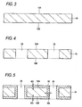
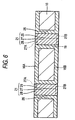
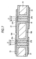
- FIG.3 to FIG.8 are views showing steps of manufacturing the wiring substrate according to the first embodiment of the present invention.
- the same reference symbols are affixed to the same constituent portions as those of the wiring substrate 10 of the first embodiment.
- the semiconductor substrate 16 shaped like a plate is prepared.
- the silicon substrate can be used as the semiconductor substrate 16.
- a thickness of the silicon substrate can be set to 200 ⁇ m, for example.
- the through holes 26 passing through the semiconductor substrate 16 are formed.
- the through holes 26 are formed by etching the semiconductor substrate 16 by means of the anisotropic etching, for example.
- the insulating film 19 is formed to cover the upper surface 16A and the lower surface 16B of the semiconductor substrate 16 and the surfaces of the semiconductor substrate 16, which are exposed from the through holes 26.
- the insulating film 19 in this case, the thermal oxide film
- the insulating film 19 formed on the upper surface 16A of the semiconductor substrate 16 constitutes the insulating film 17 (see FIG.2 ) when this insulating film 19 is etched in the step described later and shown in FIG.8 .
- the insulating film 19 formed on the lower surface 16B of the semiconductor substrate 16 constitutes the insulating film 18 (see FIG.2 ) when this insulating film 19 is etched in the step described later and shown in FIG.8 .
- a thickness of the insulating film 19 can be set to 2 ⁇ m, for example.
- the through electrodes 21 each having the through electrode main body 27, the first projection portion 28, and the second projection portion 29 are formed.
- the through electrodes 21 are formed by depositing/growing a Cu plating film in the through holes 26, on which the insulating film 19 is formed, by the plating method.
- the first wiring pattern 23 is formed on the upper surface side of the structure shown in FIG.6 to contact the first projection portion 28 and the insulating film 19.
- the second wiring pattern 24 is formed on the lower surface side of the structure shown in FIG.6 to contact the second projection portion 29 and the insulating film 19.
- a Ti film e.g., thickness of 0.1 ⁇ m
- a Cu film e.g., thickness of 0.5 ⁇ m
- a Cu film e.g., thickness of 3.0 ⁇ m
- Ni film e.g., thickness of 3.0 ⁇ m
- an Au film e.g., thickness of 0.5 ⁇ m
- the first and second wiring patterns 23, 24 constructed as above can be formed by the semi-additive process, for example.
- the first wiring pattern 23 is formed as follows. Firstly, a Ti/Cu multilayer film is formed by forming sequentially a Ti film (e.g., thickness of 0.1 ⁇ m) and a Cu film (e.g., thickness of 0.5 ⁇ m) on the first projection portion 28. Then, a resist film (not shown) having an opening portion in an area corresponding to the forming area of the first wiring pattern 23 is formed on the Ti/Cu multilayer film.
- a Cu film e.g., thickness of 3.0 ⁇ m
- a Ni film e.g., thickness of 3.0 ⁇ m
- an Au film e.g., thickness of 0.5 ⁇ m
- the resist film not shown
- portions of the Ti/Cu multilayer film covered with resist film are removed.
- the second wiring pattern 24 can be formed by the similar approach to that of the first wiring pattern 23.
- the first and second insulating films 17, 18 are formed by etching the insulating film 19 formed on the upper surface 16A and the lower surface 16B of the semiconductor substrate 16 shown in FIG.7 respectively. Also, the air gap 32 is formed between the insulating film 17 and the first wiring pattern 23, and the air gap 33 is formed between the insulating film 18 and the second wiring pattern 24. Thus, the wiring substrate 10 of the first embodiment is manufactured.
- a thickness M3 of the insulating film 19 shown in FIG.7 is set to 2 ⁇ m
- a thickness M1 of the insulating film 17 can be set to 1 ⁇ m, for example.
- a thickness M2 of the second wiring pattern 18 can be set to 1 ⁇ m, for example.
- FIG.9 is a sectional view of a wiring substrate according to a second embodiment of the present invention.
- the same reference symbols are affixed to the same constituent portions as those of the structure shown in FIG.2 .
- a wiring substrate 40 of the second embodiment includes a semiconductor substrate 41, an insulating film 42, through electrodes 45, first wiring patterns 46, first supporting members 47, second wiring patterns 48, and second supporting members 49.
- the semiconductor substrate 41 is formed like a plate. Through holes 53 are formed in the semiconductor substrate 41.
- a silicon substrate can be used, for example.
- a thickness of the silicon substrate 41 can be set to 200 ⁇ m, for example.
- the insulating film 42 is provided to cover an upper surface 41A of the semiconductor substrate 41, a lower surface 41B of the semiconductor substrate 41, and surfaces of the semiconductor substrate 41, which are exposed from the through holes 53.
- a thermal oxide film formed by thermally oxidizing the silicon substrate for example, can be used as the insulating film 42.
- a thickness of the insulating film 42 can be set to 1 ⁇ m, for example.
- a dielectric constant of the insulating film 42 is larger than a dielectric constant of the air and is about 3.8.
- the through electrode 45 is used to connect electrically the first wiring pattern 46 and the second wiring pattern 48.
- the through electrode 45 has a through electrode main body 55, a first projection portion 56, and a second projection portion 57.
- the through electrode main body 55 is provided in the through holes 53 on which the insulating film 42 is formed.
- An upper end surface 55A of the through electrode main body 55 is formed to be in the same plane as an upper surface 42A of the insulating film 42 that is formed on the upper surface 41A side of the semiconductor substrate 41.
- a lower end surface 55B of the through electrode main body 55 is formed to be in the same plane as a lower surface 42B of the insulating film 42 that is formed on the lower surface 41B side of the semiconductor substrate 41.
- As a material of the through electrode main body 55 for example, Cu can be used.
- the first projection portion 56 is provided on the upper end surface 55A of the through electrode main body 55 to project from the insulating film 42.
- the first projection portion 56 is constructed by forming sequentially a Ti film 61 formed by the sputter method, a Cu film 62 formed by the sputter method, and a Cu film 63 formed by the plating method on the upper end surface 55A of the through electrode main body 55.
- the first wiring pattern 46 connected to the electronic component 11 is provided on the Cu film 63.
- a thickness of the first projection portion 56 can be set to 5.6 ⁇ m, for example.
- a thickness of the Ti film 61 can be set to 0.1 ⁇ m
- thickness of the Cu film 62 can be set to 0.5 ⁇ m
- thickness of the Cu film 63 can be set to 5 ⁇ m.
- the first projection portion 56 constructed as above is provided such that an air whose dielectric constant (concretely, 1.0) is smaller than a dielectric constant (concretely, 3.8) of the insulating film 42 is interposed between the insulating film 42 and the first wiring pattern 46 by forming a air gap 65 (a first air gap) between the insulating film 42 and the first wiring pattern 46. That is, the first projection portion 56 is provided to improve a transmission speed of the signal transmitted between the electronic component 11 and the mounting substrate 12.
- a size of the air gap 65 can be set substantially equal to a thickness of the first projection portion 56, for example.
- a thickness of the first projection portion 56 can be set to 5.6 ⁇ m, for example.
- the first wiring pattern 46 is provided on the first projection portion 56 in a state that the air gap 65 (the first air gap) is interposed between this first wiring pattern 46 and the insulating film 42.
- the first wiring pattern 46 is constructed by forming sequentially a Cu film 67, a Ni film 68, and an Au film 69 connected to the electronic component 11 on the first projection portion 56.
- the first wiring pattern 46 is connected to the electronic component 11 and also is connected electrically to the second wiring pattern 48 via the through electrode 45.
- the Cu film 67, the Ni film 68, and the Au film 69 can be formed by the plating method, for example.
- a thickness of the Cu film 67 can be set to 5 ⁇ m, for example.
- a thickness of the Ni film 68 can be set to 3 ⁇ m, for example.
- a thickness of the Au film 69 can be set to 0.1 ⁇ m, for example.
- a plurality of first supporting members 47 are provided on portions of the insulating film 42 that faces portions of the first wiring pattern 46 which are positioned away from the first projection portion 56. The upper end of the first supporting member 47 contacts the first wiring pattern 46. A thickness of the first supporting member 47 can be set substantially equal to that of the first projection portion 56. The first supporting member 47 is used to support the first wiring pattern 46.
- the first supporting member 47 supports the first wiring pattern 46 and the thickness of the first supporting member 47 is set substantially equal to that of the first projection portion 56. Also, the first supporting member 47 is provided on portions of the insulating film 42 that faces portions of the first wiring pattern 46 which are positioned away from the first projection portion 56. Therefore, a deformation (concretely, a warp, for example) of the first wiring pattern 46 can be suppressed. As a result, a size of the air gap 65 provided between the first wiring pattern 46 and the insulating film 42 can be substantially uniform.
- the first supporting members 47 may be provided between the portion of the first wiring pattern 46, to which the electronic component 11 is connected, and the insulating film 42.
- the first supporting members 47 are provided between the portion of the first wiring pattern 46, to which the electronic component 11 is connected, and the insulating film 42. Therefore, in mounting the electronic component 11 on the first wiring pattern 46, deformation of the first wiring pattern 46 can be suppressed. As a result, the electronic component 11 can be connected (mounted) to the first wiring pattern 46 with good precision.
- the second projection portion 57 is provided on the lower end surface 55B of the through electrode main body 55 to project from the insulating film 42.
- the second projection portion 57 is constructed similarly to the first projection portion 56.
- the second projection portion 57 is constructed by forming sequentially a Ti film 61 (e.g., thickness of 0.1 ⁇ m) formed by the sputter method, a Cu film 62 (e.g., thickness of 0.5 ⁇ m) formed by the sputter method, and a Cu film 63 (e.g., thickness of 5 ⁇ m) formed by the plating method on the lower end surface 55B of the through electrode main body 55.
- the second wiring pattern 48 is provided on the Cu film 63 of the second projection portion 57 and is connected electrically to the mounting substrate 12 via the external connection terminal 14. Accordingly, a air gap 72 (a second air gap) is formed between the second wiring pattern 48 and the insulating film 42 provided on the lower surface 41B of the semiconductor substrate 41.
- the first projection portion 57 is provided to improve a transmission speed of the signal transmitted between the electronic component 11 and the mounting substrate 12 and also to improve reliability of the electrical connection between the wiring substrate 40 and the mounting substrate 12 by relaxing a difference of coefficient of thermal expansion between the mounting substrate 12 and the wiring substrate 40.
- the second wiring pattern 48 is provided on the lower end of the second projection portion 57 in a state that the air gap 72 is interposed between this second wiring pattern 48 and the insulating film 42.
- the second wiring pattern 48 is connected electrically to the second projection portion 57.
- the second wiring pattern 48 is constructed similarly to the first wiring pattern 46.
- the second wiring pattern 48 is constructed by forming sequentially a Cu film 67 (e.g., thickness of 5 ⁇ m) formed by the plating method, a Ni film 68 (e.g., thickness of 3 ⁇ m) formed by the plating method, and an Au film 69 (e.g., thickness of 0.1 ⁇ m) formed by the plating method. on the lower surface of the second projection portion 57 (concretely, the lower surface of the Cu film 63 constituting the second projection portion 57). Also, the Au film 69 is connected electrically to the pad 13 provided on the mounting substrate 12 via the external connection terminal 14.
- a plurality of second supporting members 49 are provided on portions of the insulating film 42 that faces portions of the second wiring pattern 48 which are positioned away from the second projection portion 57.
- the lower end of the second supporting member 49 contacts the second wiring pattern 48.
- a thickness of the second supporting member 49 can be set substantially equal to that of the second projection portion 57.
- the second supporting member 49 is used to support the second wiring pattern 48.
- the second supporting member 49 supports the second wiring pattern 48 and the thickness of the second supporting member 49 is set substantially equal to that of the second projection portion 57. Also, the second supporting member 49 is provided on portions of the insulating film 42 that faces portions of the second wiring pattern 48 which are positioned away from the second projection portion 57. Therefore, deformation (concretely, a warp, for example) of the second wiring pattern 48 can be suppressed. As a result, a size of the air gap 72 provided between the second wiring pattern 48 and the insulating film 42 can be substantially uniform.
- the second supporting members 49 may be provided between the portions of the second wiring pattern 48, on which the external connection terminals 14 are provided, and the insulating film 42.
- the second supporting member 49 supports the second wiring pattern 48 and the thickness of the second supporting member 49 is set substantially equal to that of the second projection portion 57. Also, the second supporting member 49 is provided on portions of the insulating film 42 that faces portions of the second wiring pattern 48 which are positioned away from the second projection portion 57. Therefore, in mounting the wiring substrate 40 on the mounting substrate 12, deformation of the second wiring pattern 48 can be suppressed. As a result, the wiring substrate 40 can be mounted on the mounting substrate 12 with good precision.
- the first supporting member 47 supports the first wiring pattern 46 and the thickness of the first supporting member 47 is set substantially equal to a that of the first projection portion 56. Also, the first supporting member 47 is provided on portions of the insulating film 42 that faces portions of the first wiring pattern 46 which are positioned away from the first projection portion 56. Furthermore, the second supporting member 49 supports the second wiring pattern 48 and the thickness of the second supporting member 49 is set substantially equal to that of the second projection portion 57. Also, the second supporting member 49 is provided on portions of the insulating film 42 that faces portions of the second wiring pattern 48 which are positioned away from the second projection portion 57. Therefore, deformations of the first and second wiring patterns 46, 48 can be suppressed respectively. As a result, sizes of the air gaps 65, 72 provided between the first and second wiring patterns 46, 48 and the insulating film 42 respectively can be substantially uniform.
- the first supporting members 47 are provided between the portion of the first wiring pattern 46, to which the electronic component 11 is connected, and the insulating film 42. Therefore, in mounting the electronic component 11 on the first wiring pattern 46, deformation of the first wiring pattern 46 can be suppressed. As a result, the electronic component 11 can be connected (mounted) to the first wiring pattern 46 with good precision.
- the second supporting members 49 is provided between the portions of the second wiring pattern 48, on which the external connection terminals 14 are provided, and the insulating film 42. Therefore, in mounting the wiring substrate 40 on the mounting substrate 12, deformation of the second wiring pattern 48 can be suppressed. As a result, the wiring substrate 40 can be mounted on the mounting substrate 12 with good precision.
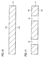
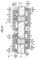
- FIG. 10 to FIG.21 are views showing steps of manufacturing the wiring substrate according to the second embodiment of the present invention.
- the same reference symbols are affixed to the same constituent portions as those of the wiring substrate 40 of the second embodiment.
- the semiconductor substrate 41 shaped like a plate is prepared.
- the silicon substrate can be used as the semiconductor substrate 41.
- a thickness of the semiconductor substrate 41 can be set to 200 ⁇ m, for example.
- the through holes 53 passing through the semiconductor substrate 41 are formed.
- the through holes 53 are formed by etching the semiconductor substrate 41 by anisotropic etching, for example.
- the insulating film 42 is formed to cover the upper surface 41A and the lower surface 41B of the semiconductor substrate 41 and surfaces of the semiconductor substrate 41, which are exposed from the through holes 53.
- the insulating film 42 (in this case, a thermal oxide film) is formed by thermally oxidizing the semiconductor substrate 41, for example.
- a thickness of the insulating film 42 can be set to 1 ⁇ m, for example.
- a dielectric constant of the insulating film 42 is larger than a dielectric constant 1.0 of the air and is about 3.8.
- the through electrode main body 55 is formed in the through holes 53 on which the insulating film 42 is formed respectively.
- the through electrode main bodies 55 are formed by depositing/growing the Cu plating film in the through holes 53, on which the insulating film 42 is formed, by the plating method.
- the upper end surface 55A of the through electrode main body 55 is formed to be in the same plane as an upper surface 42A of the insulating film 42 formed on the upper surface 41A side of the semiconductor substrate 41.
- the lower end surface 55B of the through electrode main body 55 is formed to be in the same plane as a lower surface 42B of the insulating film 42 formed on the lower surface 41B side of the semiconductor substrate 41.
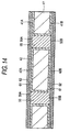
- the Ti film 61 and the Cu film 62 are formed sequentially to cover the upper surface and the lower surface of the structure shown in FIG.13 .
- the Ti film 61 and the Cu film 62 can be formed by the sputter method, for example.
- a thickness of the Ti film 61 can be set to 0.1 ⁇ m, for example.
- a thickness of the Au film 69 can be set to 0.5 ⁇ m, for example.
- a resist film 81 having opening portions 81A, 81B is formed on the upper surface of the structure shown in FIG. 14 .
- a resist film 82 having opening portions 82A, 82B is formed on the lower surface of the structure shown in FIG.14 .
- the opening portions 81A are formed to expose portions of the Cu film 62 corresponding to the forming areas of the first projection portions 56 described above.
- the opening portions 81B are formed to expose portions of the Cu film 62 corresponding to the forming areas of the first supporting members 47 described above.
- the opening portions 82A are formed to expose portions of the Cu film 62 corresponding to the forming areas of the second projection portions 57 described above. Also, the opening portions 82B are formed to expose portions of the Cu film 62 corresponding to the forming areas of the second supporting members 49 described above.
- the Cu film 63 is formed on portions of the Cu film 62, which are exposed from the opening portions 81A, 81B, 82A, 82B, by the electroplating method using the Cu film 62 as a power feeding layer.
- a thickness of the Cu film 63 can be set to 5 ⁇ m, for example.
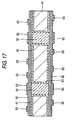
- the resist films 81, 82 shown in FIG. 16 are removed.
- a resist film 84 is formed on portions of the Cu film 62, which are positioned between the Cu films 63 formed on the upper surface side of the structure shown in FIG. 17 .
- an upper surface of the resist film 84 is formed to be in the same plane as an upper surface of the Cu film 63.
- a resist film 85 having opening portions 85A is formed on portions of the Cu film 62 on the upper surface side of the structure shown in FIG.17 .
- a resist film 87 is formed on portions of the Cu film 62, which are positioned between the Cu films 63 formed on the lower surface side of the structure shown in FIG.17 .
- an lower surface of the resist film 87 is formed to be in the same plane as a lower surface of the Cu film 63.
- a resist film 88 having opening portions 88A is formed in portions of the Cu film 62 positioned on the lower surface side of the structure shown in FIG.17 .
- the opening portions 85A are formed to expose the forming areas of the first wiring patterns 46, and the opening portions 88A are formed to expose the forming areas of the second wiring patterns 48.
- the Cu film 67, the Ni film 68, and the Au film 69 are formed sequentially on the Cu film 63 and the resist film 84 provided on the upper surface side of the structure shown in FIG.18 .
- the Cu film 67, the Ni film 68, and the Au film 69 are formed sequentially on the lower surface of the Cu film 63 and the lower surface of the resist film 87 provided on the lower surface side of the structure shown in FIG.18 .
- the Cu film 67, the Ni film 68, and the Au film 69 are formed by the electroplating method using the Cu film 62 as a power feeding layer, for example.
- the first wiring pattern 46 consisting of the Cu film 67, the Ni film 68, and the Au film 69 is formed on the upper surface side of the structure shown in FIG. 19
- the second wiring pattern 48 consisting of the Cu film 67, the Ni film 68, and the Au film 69 is formed on the lower surface side of the structure shown in FIG. 19 .
- the resist films 84, 85, 87, 88 are removed.
- steps shown in FIG.21 by removing the Cu film 62, which are not covered with the Cu film 63 provided to the structure shown in FIG.20 , and the Ti film 61, which are covered with the Cu film 62 which are not covered with the Cu film 63, the first and second supporting members 47, 49, the first and second projection portions 56, 57, and the air gaps 65, 72 are formed. As a result, the wiring substrate 40 of the second embodiment is manufactured.
Description
- The present disclosure relates to a wiring substrate, more particulary to a wiring substrate including an insulating film, e.g. for covering an upper surface and a lower surface of a semiconductor substrate, a first wiring pattern disposed on an upper surface side of the semiconductor substrate and preferably coupled to a through electrode and an electronic component, and a second wiring pattern disposed on a lower surface side of the semiconductor substrate and coupled to the through electrode and a mounting substrate.
- In the related art, as the wiring substrate (interposer) for connecting electrically the semiconductor chip and the mounting substrate such as the motherboard, a
wiring substrate 200 shown inFIG.1 is used. -
-
FIG.1 is a sectional view of a wiring substrate in the related art. - By reference to
FIG.1 , thewiring substrate 200 includes asemiconductor substrate 206 as a base material, aninsulating film 207, throughelectrodes 208, and first andsecond wirings - The
semiconductor substrate 206 is a substrate shaped like a plate, and has throughholes 215. As thesemiconductor substrate 206, for example, a silicon substrate can be used. Theinsulating film 207 is formed to cover anupper surface 206A and alower surface 206B of thesemiconductor substrate 206 and surfaces of thesemiconductor substrate 206, which are exposed from the throughholes 215. A dielectric constant of theinsulating film 207 is larger than a dielectric constant 1.0 of the air and is about 3.8. - The through
electrodes 208 are provided in the throughholes 215 on which theinsulating film 207 is formed. The throughelectrodes 208 are used to connect electrically thefirst wiring 211 and thesecond wiring 212. As the material of thethrough electrodes 208, for example, Cu can be used. - The
first wiring 211 is provided to extend over theinsulating film 207 that is formed from upper end portions of the throughelectrodes 208 to theupper surface 206A of thesemiconductor substrate 206. Thefirst wiring 211 is a wiring to which anelectronic component 201 is connected (mounted). As theelectronic component 201, the semiconductor chip whose base material is formed of the silicon substrate can be used. - The
second wiring 212 is provided to extend over the lower surface of theinsulating film 207 that is formed from lower end portions of the throughelectrodes 208 to thelower surface 206B of thesemiconductor substrate 206. Thesecond wiring 212 is a wiring that is connected electrically to pads 203 of a mounting substrate 202 (concretely, the mother board, for example). As the material of the base member of themounting substrate 202, a resin can be used (see e.g.,JP-A-2007-42741 - However, in the
wiring substrate 200 in the related art, the first andsecond wirings insulating film 207. Therefore, there is a problem that a transmission speed of a signal transmitted between theelectronic component 201 connected to thefirst wiring 211 and themounting substrate 202 connected electrically to thesecond wiring 212 cannot be increased. - Also, a material of the base member (concretely, silicon) of the
wiring substrate 200 is different from that of the base member (concretely, resin) of themounting substrate 202. Therefore, there is a problem that reliability of electrical connection between thewiring substrate 200 and themounting substrate 202 is decreased on account of a difference of coefficient of thermal expansion between thewiring substrate 200 and themounting substrate 202. - Exemplary embodiments of the present invention address the above disadvantages and other disadvantages not described above. However, the present invention is not required to overcome the disadvantages described above, and thus, an exemplary embodiment of the present invention may not overcome any of the problems described above. In view of the above, a wiring substrate according to
claim 1, a semiconductor device according to claim 9, and a method according toclaim 11 is provided. - It is an aspect of the present invention to provide a wiring substrate capable of improving a transmission speed of a signal transmitted between an electronic component and a mounting substrate and capable of improving reliability of electrical connection between the wiring substrate and the mounting substrate.
- According to one or more aspects of the present invention, there is provided a wiring substrate. The wiring substrate includes: a semiconductor substrate having a through hole; an insulating film provided to cover an upper surface, a lower surface and a first surface of the semiconductor substrate, the first surface corresponding to a side surface of the through hole; a through electrode provided in the through hole; a first wiring pattern disposed on an upper surface side of the semiconductor substrate and coupled to the through electrode; and a second wiring pattern disposed on a lower surface side of the semiconductor substrate and coupled to the through electrode. A first air gap is provided between the first wiring pattern and the insulating film formed on the upper surface, and a second air gap is provided between the second wiring pattern and the insulating film formed on the lower surface.
- According to one or more aspects of the present invention, there is provided a semiconductor device including the wiring substrate, and an electronic component coupled to the first wiring pattern.
- According to one or more aspects of the present invention, in a method of manufacturing a wiring substrate, the method includes: i) preparing a semiconductor substrate; ii) forming a through hole in the semiconductor substrate; iii) forming an insulating film on an upper surface, a lower surface and a first surface of the semiconductor substrate, the first surface corresponding to a side surface of the through hole; iv) providing a through electrode in the trough hole; v) forming a first wiring pattern on the insulating film formed on the upper surface such that the first wiring pattern is coupled to the through electrode; vi) forming a second wiring pattern on the insulting film formed on the lower surface such that the second wiring pattern is coupled to the through electrode; vii) etching the insulating film formed on the upper surface, thereby forming an air gap between the first wiring pattern and the insulating film formed on the upper surface; and viii) etching the insulating film formed on the lower surface, thereby forming an air gap between the second wiring pattern and the insulating film formed on the lower surface.
- Other aspects and advantages of the invention will be apparent from the following description, the drawings and the claims.
The invention is also directed to apparatuses for carrying out the disclosed methods and including apparatus parts for performing each described method steps. These method steps may be performed by way of hardware components, a computer programmed by appropriate software, by any combination of the two or in any other manner. Furthermore, the invention is also directed to methods by which the described apparatus operates. It includes method steps for carrying out every function of the apparatus or manufacturing every part of the apparatus. - The above and other aspects, features and advantages of the present invention will be more apparent from the following more particular description thereof, presented in conjunction with the following drawings wherein:
-
FIG.1 is a sectional view of a wiring substrate in the related art; -
FIG.2 is a sectional view of a wiring substrate according to a first embodiment of the present invention; -
FIG.3 is a view (#1) showing steps of manufacturing the wiring substrate according to the first embodiment of the present invention; -
FIG.4 is a view (#2) showing steps of manufacturing the wiring substrate according to the first embodiment of the present invention; -
FIG.5 is a view (#3) showing steps of manufacturing the wiring substrate according to the first embodiment of the present invention; -
FIG.6 is a view (#4) showing steps of manufacturing the wiring substrate according to the first embodiment of the present invention; -
FIG.7 is a view (#5) showing steps of manufacturing the wiring substrate according to the first embodiment of the present invention; -
FIG.8 is a view (#6) showing steps of manufacturing the wiring substrate according to the first embodiment of the present invention; -
FIG.9 is a sectional view of a wiring substrate according to a second embodiment of the present invention; -
FIG.10 is a view (#1) showing steps of manufacturing the wiring substrate according to the second embodiment of the present invention; -
FIG.11 is a view (#2) showing steps of manufacturing the wiring substrate according to the second embodiment of the present invention; -
FIG.12 is a view (#3) showing steps of manufacturing the wiring substrate according to the second embodiment of the present invention; -
FIG.13 is a view (#4) showing steps of manufacturing the wiring substrate according to the second embodiment of the present invention; -
FIG.14 is a view (#5) showing steps of manufacturing the wiring substrate according to the second embodiment of the present invention; -
FIG.15 is a view (#6) showing steps of manufacturing the wiring substrate according to the second embodiment of the present invention; -
FIG.16 is a view (#7) showing steps of manufacturing the wiring substrate according to the second embodiment of the present invention; -
FIG.17 is a view (#8) showing steps of manufacturing the wiring substrate according to the second embodiment of the present invention; -
FIG.18 is a view (#9) showing steps of manufacturing the wiring substrate according to the second embodiment of the present invention; - [
FIG.19 is a view (#10) showing steps of manufacturing the wiring substrate according to the second embodiment of the present invention; -
FIG.20 is a view (#11) showing steps of manufacturing the wiring substrate according to the second embodiment of the present invention; and -
FIG.21 is a view (#12) showing steps of manufacturing the wiring substrate according to the second embodiment of the present invention. - Exemplary embodiments of the present invention will be described with reference to the drawings hereinafter.
-
FIG.2 is a sectional view of a wiring substrate according to a first embodiment of the present invention. - By reference to
FIG.2 , awiring substrate 10 of the first embodiment includes asemiconductor substrate 16,insulating films 17 to 19, throughholes 21,first wiring patterns 23, andsecond wiring patterns 24. - The
semiconductor substrate 16 is formed like a plate. The plurality of throughholes 26 are formed in thesemiconductor substrate 16. As thesemiconductor substrate 16, a silicon substrate can be used, for example. When the silicon substrate is used as thesemiconductor substrate 16, a thickness of thesilicon substrate 16 can be set to 200 µm, for example. - The insulating
film 16 is provided to cover anupper face 16A of thesemiconductor substrate 16. When the silicon substrate is used as thesemiconductor substrate 16, a thermal oxide film formed by thermally oxidizing the silicon substrate, for example, can be used as the insulatingfilm 17. A thickness M1 of the insulatingfilm 17 can be set to 1 µm, for example. A dielectric constant of the insulatingfilm 17 is larger than a dielectric constant 1.0 of the air and is about 3.8. - The insulating
film 18 is provided to cover alower face 16B of thesemiconductor substrate 16. When the silicon substrate is used as thesemiconductor substrate 16, a thermal oxide film formed by thermally oxidizing the silicon substrate, for example, can be used as the insulatingfilm 18. A thickness M2 of the insulatingfilm 18 can be set to 1 µm, for example. A dielectric constant of the insulatingfilm 18 is larger than a dielectric constant 1.0 of the air and is about 3.8. - The insulating
film 19 is provided to cover surfaces of thesemiconductor substrate 16, which are exposed from the through holes 26. The insulatingfilm 19 is used to insulate a through electrodemain body 27, as described below, and thesemiconductor substrate 16. When the silicon substrate is used as thesemiconductor substrate 16, a thermal oxide film formed by thermally oxidizing the silicon substrate, for example, can be used as the insulatingfilm 19. A thickness M3 of the insulatingfilm 19 can be set to 2 µm, for example. - The through
electrode 21 is used to connect electrically thefirst wiring pattern 23 and thesecond wiring pattern 24. The throughelectrode 21 has the through electrodemain body 27, afirst projection portion 28, and asecond projection portion 29. The through electrodemain body 27 is provided in the throughhole 26 on which the insulatingfilm 19 is formed. Anupper end surface 27A of the through electrodemain body 27 is formed in the substantially same plane as anupper surface 17A of the insulatingfilm 17. Alower end surface 27B of the through electrodemain body 27 is formed in the substantially same plane as alower surface 18A of the insulatingfilm 18. As a material of the through electrodemain body 27, for example, Cu can be used. - The
first projection portion 28 is provided on theupper end surface 27A of the through electrodemain body 27. Thefirst projection portion 28 is formed integrally with the through electrodemain body 27. Thefirst projection portion 28 projects from the insulatingfilm 17. Thefirst wiring pattern 23 connected to an electronic component 11 (concretely, a semiconductor chip such as IC, LSI) is provided on the upper surface of thefirst projection portion 28. Thefirst projection portion 28 is provided to form an air gap 32 (a first air gap) between the insulatingfilm 17 and thefirst wiring pattern 23. A size of theair gap 32 can be set to 1 µm, for example. A thickness of thefirst projection portion 28 can be set to a value substantially equal to a value of theair gap 32. Concretely, when a size of theair gap 32 is 1 µm, a thickness of thefirst projection portion 28 can be set to 1 µm, for example. As the material of thefirst projection portion 28, for example, Cu can be used. - In this manner, the
air gap 32 is formed between the insulatingfilm 17 and thefirst wiring pattern 23 by providing thefirst projection portion 28, which projects from the insulatingfilm 17, to the throughelectrode 21. Thus, an air whose dielectric constant (concretely, 1.0) is smaller than a dielectric constant (concretely, 3.8) of the insulatingfilm 17 can be interposed between the insulatingfilm 17 and thefirst wiring pattern 23. Therefore, a transmission speed of the signal transmitted between theelectronic component 11 and a mountingsubstrate 12 can be improved. - The
second projection portion 29 is provided on thelower end surface 27B of the through electrodemain body 27. Thesecond projection portion 29 is formed integrally with the through electrodemain body 27. Thesecond projection portion 29 projects from the insulatingfilm 18. Thesecond wiring pattern 24 connected to the mounting substrate 12 (concretely, the motherboard, for example) is provided on the lower surface of thesecond projection portion 29. Thesecond projection portion 29 is provided to form a air gap 33 (a second air gap) between the insulatingfilm 18 and thesecond wiring pattern 24. A size of theair gap 33 can be set to 1 µm, for example. A thickness of thesecond projection portion 29 can be set to a value substantially equal to a value of theair gap 33. Concretely, when a size of theair gap 33 is 1 µm, a thickness of thesecond projection portion 29 can be set to 1 µm, for example. As the material of thesecond projection portion 29, for example, Cu can be used. - In this manner, the
air gap 33 is formed between the insulatingfilm 18 and thesecond wiring pattern 24 by providing thesecond projection portion 29, which projects from the insulatingfilm 18, to the throughelectrode 21. Thus, an air whose dielectric constant (concretely, 1.0) is smaller than a dielectric constant (concretely, 3.8) of the insulatingfilm 18 can be interposed between the insulatingfilm 18 and thesecond wiring pattern 24. Therefore, a transmission speed of the signal transmitted between theelectronic component 11 and the mountingsubstrate 12 can be improved. - Also, the
second wiring pattern 24 is positioned away from the insulatingfilm 18 by providing theair gap 33 between the insulatingfilm 18 and thesecond wiring pattern 24 to which the mountingsubstrate 12 is connected. Thus, a difference of coefficient of thermal expansion between thewiring substrate 10 and the mountingsubstrate 12 can be relaxed. Therefore, reliability of the electrical connection between thewiring substrate 10 and the mountingsubstrate 12 can be improved. - The
first wiring pattern 23 is provided on thefirst projection portion 28 in a state that theair gap 32 is interposed between thisfirst wiring pattern 23 and the insulatingfilm 17 formed on theupper surface 16A of thesemiconductor substrate 16. Thefirst wiring pattern 23 is used to connect (mount) theelectronic component 11. Thefirst wiring pattern 23 is connected electrically to thesecond wiring pattern 24 via the throughelectrode 21. As thefirst wiring pattern 23, for example, a multilayer film constructed by forming sequentially a Ti film (e.g., thickness of 0.1 µm) formed by the sputter method, a Cu film (e.g., thickness of 0.5 µm) formed by the sputter method, a Cu film (e.g., thickness of 3.0 µm) formed by the plating method, a Ni film (e.g., thickness of 3.0 µm) formed by the plating method, and an Au film (e.g., thickness of 0.5 µm) formed by the plating method on thefirst projection portion 28 can be used. - The
second wiring pattern 24 is provided on thelower surface 16B of thesemiconductor substrate 16 in a state that theair gap 33 is interposed between thissecond wiring pattern 24 and the insulatingfilm 18 formed on thelower surface 16B of thesemiconductor substrate 16. Thesecond wiring pattern 24 is connected to apad 13 provided to the mountingsubstrate 12 via an external connection terminal 14 (e.g., a solder bump), and also is connected electrically to thefirst wiring pattern 23 via the throughelectrode 21. As thesecond wiring pattern 24, for example, a multilayer film constructed by forming sequentially a Ti film (e.g., thickness of 0.1 µm) formed by the sputter method, a Cu film (e.g., thickness of 0.5 µm) formed by the sputter method, a Cu film (e.g., thickness of 3.0 µm) formed by the plating method, a Ni film (e.g., thickness of 3.0 µm) formed by the plating method, and an Au film (e.g., thickness of 0.5 µm) formed by the plating method on the lower surface of thesecond projection portion 29 can be used. - According to the wiring substrate of the present embodiment, the
first wiring pattern 23 connected to theelectronic component 11 is provided on thefirst projection portion 28, which projects from the insulatingfilm 17 formed on theupper surface 16A of thesemiconductor substrate 16, such that theair gap 32 is formed between the insulatingfilm 17 and thefirst wiring pattern 23. Also, thesecond wiring pattern 24 connected electrically to the mountingsubstrate 12 is provided on the lower surface of thesecond projection portion 29, which projects from the insulatingfilm 18 formed on thelower surface 16B of thesemiconductor substrate 16, such that theair gap 33 is formed between the insulatingfilm 18 and thesecond wiring pattern 24. Therefore, an air whose dielectric constant (concretely, 1.0) is smaller than a dielectric constant (concretely, 3.8) of the insulatingfilms film 17 and thefirst wiring pattern 23 and between the insulatingfilm 18 and thesecond wiring pattern 24 respectively. As a result, a transmission speed of the signal transmitted between theelectronic component 11 and the mountingsubstrate 12 can be improved. - Also, the
second wiring pattern 24 is positioned away from the insulatingfilm 18 by providing theair gap 33 between the insulatingfilm 18 and thesecond wiring pattern 24 to which the mountingsubstrate 12 is connected. Thus, a difference of coefficient of thermal expansion between thewiring substrate 10 and the mountingsubstrate 12 can be relaxed. Therefore, reliability of the electrical connection between thewiring substrate 10 and the mountingsubstrate 12 can be improved. - Also, the
wiring substrate 10 of the present embodiment has been described in connection with the case where theair gap 32 is formed between thefirst wiring pattern 23 and the insulatingfilm 17 and theair gap 33 is formed between thesecond wiring pattern 24 and the insulatingfilm 18. Only any one air gap out of theair gaps air gap 32 is formed, a transmission speed of the signal transmitted between theelectronic component 11 and the mountingsubstrate 12 can be improved. Also, for example, when only theair gap 33 is formed, a transmission speed of the signal transmitted between theelectronic component 11 and the mountingsubstrate 12 can be improved (this case is inferior in a degree of improvement to the case where both of theair gaps wiring substrate 10 and the mountingsubstrate 12 can be improved. -
FIG.3 to FIG.8 are views showing steps of manufacturing the wiring substrate according to the first embodiment of the present invention. InFIG.3 to FIG.8 , the same reference symbols are affixed to the same constituent portions as those of thewiring substrate 10 of the first embodiment. - At first, in steps shown in
FIG.3 , thesemiconductor substrate 16 shaped like a plate is prepared. As thesemiconductor substrate 16, for example, the silicon substrate can be used. When the silicon substrate is used as thesemiconductor substrate 16, a thickness of the silicon substrate can be set to 200 µm, for example. - Then, in steps shown in
FIG.4 , the throughholes 26 passing through thesemiconductor substrate 16 are formed. Concretely, the throughholes 26 are formed by etching thesemiconductor substrate 16 by means of the anisotropic etching, for example. - Then, in steps shown in
FIG.5 , the insulatingfilm 19 is formed to cover theupper surface 16A and thelower surface 16B of thesemiconductor substrate 16 and the surfaces of thesemiconductor substrate 16, which are exposed from the through holes 26. Concretely, when the silicon substrate is used as thesemiconductor substrate 16, the insulating film 19 (in this case, the thermal oxide film) is formed by thermally oxidizing thesemiconductor substrate 16, for example. In this event, the insulatingfilm 19 formed on theupper surface 16A of thesemiconductor substrate 16 constitutes the insulating film 17 (seeFIG.2 ) when this insulatingfilm 19 is etched in the step described later and shown inFIG.8 . Also, the insulatingfilm 19 formed on thelower surface 16B of thesemiconductor substrate 16 constitutes the insulating film 18 (seeFIG.2 ) when this insulatingfilm 19 is etched in the step described later and shown inFIG.8 . A thickness of the insulatingfilm 19 can be set to 2 µm, for example. - Then, in steps shown in
FIG.6 , the throughelectrodes 21 each having the through electrodemain body 27, thefirst projection portion 28, and thesecond projection portion 29 are formed. Concretely, the throughelectrodes 21 are formed by depositing/growing a Cu plating film in the throughholes 26, on which the insulatingfilm 19 is formed, by the plating method. - Then, in steps shown in
FIG.7 , thefirst wiring pattern 23 is formed on the upper surface side of the structure shown inFIG.6 to contact thefirst projection portion 28 and the insulatingfilm 19. Also, thesecond wiring pattern 24 is formed on the lower surface side of the structure shown inFIG.6 to contact thesecond projection portion 29 and the insulatingfilm 19. As thefirst wiring pattern 23, for example, the multilayer film constructed by forming in sequence a Ti film (e.g., thickness of 0.1 µm) formed by the sputter method, a Cu film (e.g., thickness of 0.5 µm) formed by the sputter method, a Cu film (e.g., thickness of 3.0 µm) formed by the plating method, a Ni film (e.g., thickness of 3.0 µm) formed by the plating method, and an Au film (e.g., thickness of 0.5 µm) formed by the plating method on thefirst projection portion 28 can be used. - Also, as the
second wiring pattern 24, for example, the multilayer film constructed by forming in sequence a Ti film (e.g., thickness of 0.1 µm) formed by the sputter method, a Cu film (e.g., thickness of 0.5 µm) formed by the sputter method, a Cu film (e.g., thickness of 3.0 µm) formed by the plating method, a Ni film (e.g., thickness of 3.0 µm) formed by the plating method, and an Au film (e.g., thickness of 0.5 µm) formed by the plating method on the lower surface of thesecond projection portion 29 can be used. - The first and
second wiring patterns first wiring pattern 23 is formed as follows. Firstly, a Ti/Cu multilayer film is formed by forming sequentially a Ti film (e.g., thickness of 0.1 µm) and a Cu film (e.g., thickness of 0.5 µm) on thefirst projection portion 28. Then, a resist film (not shown) having an opening portion in an area corresponding to the forming area of thefirst wiring pattern 23 is formed on the Ti/Cu multilayer film. Then, a Cu film (e.g., thickness of 3.0 µm), a Ni film (e.g., thickness of 3.0 µm), and an Au film (e.g., thickness of 0.5 µm) are formed sequentially on the Ti/Cu multilayer film by the electroplating method using the Ti/Cu multilayer film as a power feeding layer. Finally, the resist film (not shown) and portions of the Ti/Cu multilayer film covered with resist film (not shown) are removed. Also, thesecond wiring pattern 24 can be formed by the similar approach to that of thefirst wiring pattern 23. - Then, in steps shown in
FIG.8 , the first and second insulatingfilms film 19 formed on theupper surface 16A and thelower surface 16B of thesemiconductor substrate 16 shown inFIG.7 respectively. Also, theair gap 32 is formed between the insulatingfilm 17 and thefirst wiring pattern 23, and theair gap 33 is formed between the insulatingfilm 18 and thesecond wiring pattern 24. Thus, thewiring substrate 10 of the first embodiment is manufactured. When a thickness M3 of the insulatingfilm 19 shown inFIG.7 is set to 2 µm, a thickness M1 of the insulatingfilm 17 can be set to 1 µm, for example. In this case, a thickness M2 of thesecond wiring pattern 18 can be set to 1 µm, for example. -
FIG.9 is a sectional view of a wiring substrate according to a second embodiment of the present invention. InFIG.9 , the same reference symbols are affixed to the same constituent portions as those of the structure shown inFIG.2 . - By reference to
FIG.9 , awiring substrate 40 of the second embodiment includes asemiconductor substrate 41, an insulatingfilm 42, throughelectrodes 45,first wiring patterns 46, first supportingmembers 47,second wiring patterns 48, and second supportingmembers 49. - The
semiconductor substrate 41 is formed like a plate. Throughholes 53 are formed in thesemiconductor substrate 41. As thesemiconductor substrate 41, a silicon substrate can be used, for example. When the silicon substrate is used as thesemiconductor substrate 41, a thickness of thesilicon substrate 41 can be set to 200 µm, for example. - The insulating
film 42 is provided to cover anupper surface 41A of thesemiconductor substrate 41, alower surface 41B of thesemiconductor substrate 41, and surfaces of thesemiconductor substrate 41, which are exposed from the through holes 53. When the silicon substrate is used as thesemiconductor substrate 41, a thermal oxide film formed by thermally oxidizing the silicon substrate, for example, can be used as the insulatingfilm 42. A thickness of the insulatingfilm 42 can be set to 1 µm, for example. A dielectric constant of the insulatingfilm 42 is larger than a dielectric constant of the air and is about 3.8. - The through
electrode 45 is used to connect electrically thefirst wiring pattern 46 and thesecond wiring pattern 48. The throughelectrode 45 has a through electrodemain body 55, afirst projection portion 56, and asecond projection portion 57. The through electrodemain body 55 is provided in the throughholes 53 on which the insulatingfilm 42 is formed. Anupper end surface 55A of the through electrodemain body 55 is formed to be in the same plane as anupper surface 42A of the insulatingfilm 42 that is formed on theupper surface 41A side of thesemiconductor substrate 41. Alower end surface 55B of the through electrodemain body 55 is formed to be in the same plane as alower surface 42B of the insulatingfilm 42 that is formed on thelower surface 41B side of thesemiconductor substrate 41. As a material of the through electrodemain body 55, for example, Cu can be used. - The
first projection portion 56 is provided on theupper end surface 55A of the through electrodemain body 55 to project from the insulatingfilm 42. Thefirst projection portion 56 is constructed by forming sequentially aTi film 61 formed by the sputter method, aCu film 62 formed by the sputter method, and aCu film 63 formed by the plating method on theupper end surface 55A of the through electrodemain body 55. Thefirst wiring pattern 46 connected to theelectronic component 11 is provided on theCu film 63. A thickness of thefirst projection portion 56 can be set to 5.6 µm, for example. In this case, as respective thicknesses of the films constituting thefirst projection portion 56, for example, a thickness of theTi film 61 can be set to 0.1 µm, thickness of theCu film 62 can be set to 0.5 µm, and thickness of theCu film 63 can be set to 5 µm. - The
first projection portion 56 constructed as above is provided such that an air whose dielectric constant (concretely, 1.0) is smaller than a dielectric constant (concretely, 3.8) of the insulatingfilm 42 is interposed between the insulatingfilm 42 and thefirst wiring pattern 46 by forming a air gap 65 (a first air gap) between the insulatingfilm 42 and thefirst wiring pattern 46. That is, thefirst projection portion 56 is provided to improve a transmission speed of the signal transmitted between theelectronic component 11 and the mountingsubstrate 12. A size of theair gap 65 can be set substantially equal to a thickness of thefirst projection portion 56, for example. A thickness of thefirst projection portion 56 can be set to 5.6 µm, for example. - The
first wiring pattern 46 is provided on thefirst projection portion 56 in a state that the air gap 65 (the first air gap) is interposed between thisfirst wiring pattern 46 and the insulatingfilm 42. Thefirst wiring pattern 46 is constructed by forming sequentially aCu film 67, aNi film 68, and anAu film 69 connected to theelectronic component 11 on thefirst projection portion 56. Thefirst wiring pattern 46 is connected to theelectronic component 11 and also is connected electrically to thesecond wiring pattern 48 via the throughelectrode 45. TheCu film 67, theNi film 68, and theAu film 69 can be formed by the plating method, for example. A thickness of theCu film 67 can be set to 5 µm, for example. A thickness of theNi film 68 can be set to 3 µm, for example. Also, a thickness of theAu film 69 can be set to 0.1 µm, for example. - A plurality of first supporting
members 47 are provided on portions of the insulatingfilm 42 that faces portions of thefirst wiring pattern 46 which are positioned away from thefirst projection portion 56. The upper end of the first supportingmember 47 contacts thefirst wiring pattern 46. A thickness of the first supportingmember 47 can be set substantially equal to that of thefirst projection portion 56. The first supportingmember 47 is used to support thefirst wiring pattern 46. - In this manner, the first supporting
member 47 supports thefirst wiring pattern 46 and the thickness of the first supportingmember 47 is set substantially equal to that of thefirst projection portion 56. Also, the first supportingmember 47 is provided on portions of the insulatingfilm 42 that faces portions of thefirst wiring pattern 46 which are positioned away from thefirst projection portion 56. Therefore, a deformation (concretely, a warp, for example) of thefirst wiring pattern 46 can be suppressed. As a result, a size of theair gap 65 provided between thefirst wiring pattern 46 and the insulatingfilm 42 can be substantially uniform. - Also, the first supporting
members 47 may be provided between the portion of thefirst wiring pattern 46, to which theelectronic component 11 is connected, and the insulatingfilm 42. - In this manner, the first supporting
members 47 are provided between the portion of thefirst wiring pattern 46, to which theelectronic component 11 is connected, and the insulatingfilm 42. Therefore, in mounting theelectronic component 11 on thefirst wiring pattern 46, deformation of thefirst wiring pattern 46 can be suppressed. As a result, theelectronic component 11 can be connected (mounted) to thefirst wiring pattern 46 with good precision. - The
second projection portion 57 is provided on thelower end surface 55B of the through electrodemain body 55 to project from the insulatingfilm 42. Thesecond projection portion 57 is constructed similarly to thefirst projection portion 56. Concretely, thesecond projection portion 57 is constructed by forming sequentially a Ti film 61 (e.g., thickness of 0.1 µm) formed by the sputter method, a Cu film 62 (e.g., thickness of 0.5 µm) formed by the sputter method, and a Cu film 63 (e.g., thickness of 5 µm) formed by the plating method on thelower end surface 55B of the through electrodemain body 55. Thesecond wiring pattern 48 is provided on theCu film 63 of thesecond projection portion 57 and is connected electrically to the mountingsubstrate 12 via theexternal connection terminal 14. Accordingly, a air gap 72 (a second air gap) is formed between thesecond wiring pattern 48 and the insulatingfilm 42 provided on thelower surface 41B of thesemiconductor substrate 41. - In the
second projection portion 57 constructed as above, an air whose dielectric constant (concretely, 1.0) is smaller than a dielectric constant (concretely, 3.8) of the insulatingfilm 42 is interposed between the insulatingfilm 42 and thesecond wiring pattern 47 by forming the air gap 72 (the second air gap) between the insulatingfilm 42 and thesecond wiring pattern 47. That is, thefirst projection portion 57 is provided to improve a transmission speed of the signal transmitted between theelectronic component 11 and the mountingsubstrate 12 and also to improve reliability of the electrical connection between thewiring substrate 40 and the mountingsubstrate 12 by relaxing a difference of coefficient of thermal expansion between the mountingsubstrate 12 and thewiring substrate 40. - The
second wiring pattern 48 is provided on the lower end of thesecond projection portion 57 in a state that theair gap 72 is interposed between thissecond wiring pattern 48 and the insulatingfilm 42. Thesecond wiring pattern 48 is connected electrically to thesecond projection portion 57. Thesecond wiring pattern 48 is constructed similarly to thefirst wiring pattern 46. Concretely, thesecond wiring pattern 48 is constructed by forming sequentially a Cu film 67 (e.g., thickness of 5 µm) formed by the plating method, a Ni film 68 (e.g., thickness of 3 µm) formed by the plating method, and an Au film 69 (e.g., thickness of 0.1 µm) formed by the plating method. on the lower surface of the second projection portion 57 (concretely, the lower surface of theCu film 63 constituting the second projection portion 57). Also, theAu film 69 is connected electrically to thepad 13 provided on the mountingsubstrate 12 via theexternal connection terminal 14. - A plurality of second supporting
members 49 are provided on portions of the insulatingfilm 42 that faces portions of thesecond wiring pattern 48 which are positioned away from thesecond projection portion 57. The lower end of the second supportingmember 49 contacts thesecond wiring pattern 48. A thickness of the second supportingmember 49 can be set substantially equal to that of thesecond projection portion 57. The second supportingmember 49 is used to support thesecond wiring pattern 48. - In this manner, the second supporting
member 49 supports thesecond wiring pattern 48 and the thickness of the second supportingmember 49 is set substantially equal to that of thesecond projection portion 57. Also, the second supportingmember 49 is provided on portions of the insulatingfilm 42 that faces portions of thesecond wiring pattern 48 which are positioned away from thesecond projection portion 57. Therefore, deformation (concretely, a warp, for example) of thesecond wiring pattern 48 can be suppressed. As a result, a size of theair gap 72 provided between thesecond wiring pattern 48 and the insulatingfilm 42 can be substantially uniform. - Also, the second supporting
members 49 may be provided between the portions of thesecond wiring pattern 48, on which theexternal connection terminals 14 are provided, and the insulatingfilm 42. - In this manner, the second supporting
member 49 supports thesecond wiring pattern 48 and the thickness of the second supportingmember 49 is set substantially equal to that of thesecond projection portion 57. Also, the second supportingmember 49 is provided on portions of the insulatingfilm 42 that faces portions of thesecond wiring pattern 48 which are positioned away from thesecond projection portion 57. Therefore, in mounting thewiring substrate 40 on the mountingsubstrate 12, deformation of thesecond wiring pattern 48 can be suppressed. As a result, thewiring substrate 40 can be mounted on the mountingsubstrate 12 with good precision. - According to the wiring substrate of the present embodiment, the first supporting
member 47 supports thefirst wiring pattern 46 and the thickness of the first supportingmember 47 is set substantially equal to a that of thefirst projection portion 56. Also, the first supportingmember 47 is provided on portions of the insulatingfilm 42 that faces portions of thefirst wiring pattern 46 which are positioned away from thefirst projection portion 56. Furthermore, the second supportingmember 49 supports thesecond wiring pattern 48 and the thickness of the second supportingmember 49 is set substantially equal to that of thesecond projection portion 57. Also, the second supportingmember 49 is provided on portions of the insulatingfilm 42 that faces portions of thesecond wiring pattern 48 which are positioned away from thesecond projection portion 57. Therefore, deformations of the first andsecond wiring patterns air gaps second wiring patterns film 42 respectively can be substantially uniform. - Also, the first supporting
members 47 are provided between the portion of thefirst wiring pattern 46, to which theelectronic component 11 is connected, and the insulatingfilm 42. Therefore, in mounting theelectronic component 11 on thefirst wiring pattern 46, deformation of thefirst wiring pattern 46 can be suppressed. As a result, theelectronic component 11 can be connected (mounted) to thefirst wiring pattern 46 with good precision. - In addition, the second supporting
members 49 is provided between the portions of thesecond wiring pattern 48, on which theexternal connection terminals 14 are provided, and the insulatingfilm 42. Therefore, in mounting thewiring substrate 40 on the mountingsubstrate 12, deformation of thesecond wiring pattern 48 can be suppressed. As a result, thewiring substrate 40 can be mounted on the mountingsubstrate 12 with good precision. -
FIG. 10 to FIG.21 are views showing steps of manufacturing the wiring substrate according to the second embodiment of the present invention. InFIG.10 to FIG.21 , the same reference symbols are affixed to the same constituent portions as those of thewiring substrate 40 of the second embodiment. - At first, in steps shown in
FIG.10 , thesemiconductor substrate 41 shaped like a plate is prepared. As thesemiconductor substrate 41, for example, the silicon substrate can be used. When the silicon substrate is used as thesemiconductor substrate 41, a thickness of thesemiconductor substrate 41 can be set to 200 µm, for example. - Then, in steps shown in
FIG.11 , the throughholes 53 passing through thesemiconductor substrate 41 are formed. Concretely, the throughholes 53 are formed by etching thesemiconductor substrate 41 by anisotropic etching, for example. - Then, in steps shown in
FIG.12 , the insulatingfilm 42 is formed to cover theupper surface 41A and thelower surface 41B of thesemiconductor substrate 41 and surfaces of thesemiconductor substrate 41, which are exposed from the through holes 53. Concretely, when the silicon substrate is used as thesemiconductor substrate 41, the insulating film 42 (in this case, a thermal oxide film) is formed by thermally oxidizing thesemiconductor substrate 41, for example. A thickness of the insulatingfilm 42 can be set to 1 µm, for example. A dielectric constant of the insulatingfilm 42 is larger than a dielectric constant 1.0 of the air and is about 3.8. - Then, in steps shown in
FIG.13 , the through electrodemain body 55 is formed in the throughholes 53 on which the insulatingfilm 42 is formed respectively. Concretely, the through electrodemain bodies 55 are formed by depositing/growing the Cu plating film in the throughholes 53, on which the insulatingfilm 42 is formed, by the plating method. At this time, theupper end surface 55A of the through electrodemain body 55 is formed to be in the same plane as anupper surface 42A of the insulatingfilm 42 formed on theupper surface 41A side of thesemiconductor substrate 41. Also, thelower end surface 55B of the through electrodemain body 55 is formed to be in the same plane as alower surface 42B of the insulatingfilm 42 formed on thelower surface 41B side of thesemiconductor substrate 41. - Then, in steps shown in
FIG. 14 , theTi film 61 and theCu film 62 are formed sequentially to cover the upper surface and the lower surface of the structure shown inFIG.13 . Concretely, theTi film 61 and theCu film 62 can be formed by the sputter method, for example. A thickness of theTi film 61 can be set to 0.1 µm, for example. A thickness of theAu film 69 can be set to 0.5 µm, for example. - Then, in steps shown in
FIG.15 , a resistfilm 81 havingopening portions FIG. 14 . Also, a resistfilm 82 havingopening portions FIG.14 . The openingportions 81A are formed to expose portions of theCu film 62 corresponding to the forming areas of thefirst projection portions 56 described above. Also, the openingportions 81B are formed to expose portions of theCu film 62 corresponding to the forming areas of the first supportingmembers 47 described above. - The opening
portions 82A are formed to expose portions of theCu film 62 corresponding to the forming areas of thesecond projection portions 57 described above. Also, the openingportions 82B are formed to expose portions of theCu film 62 corresponding to the forming areas of the second supportingmembers 49 described above. - Then, in steps shown in
FIG.16 , theCu film 63 is formed on portions of theCu film 62, which are exposed from the openingportions Cu film 62 as a power feeding layer. A thickness of theCu film 63 can be set to 5 µm, for example. Then, in steps shown inFIG. 17 , the resistfilms FIG. 16 are removed. - Then, in steps shown in
FIG. 18 , a resistfilm 84 is formed on portions of theCu film 62, which are positioned between theCu films 63 formed on the upper surface side of the structure shown inFIG. 17 . In this case, an upper surface of the resistfilm 84 is formed to be in the same plane as an upper surface of theCu film 63. Also, a resistfilm 85 havingopening portions 85A is formed on portions of theCu film 62 on the upper surface side of the structure shown inFIG.17 . Also, in steps shown inFIG.18 , a resistfilm 87 is formed on portions of theCu film 62, which are positioned between theCu films 63 formed on the lower surface side of the structure shown inFIG.17 . In this case, an lower surface of the resistfilm 87 is formed to be in the same plane as a lower surface of theCu film 63. Also, a resistfilm 88 havingopening portions 88A is formed in portions of theCu film 62 positioned on the lower surface side of the structure shown inFIG.17 . The openingportions 85A are formed to expose the forming areas of thefirst wiring patterns 46, and the openingportions 88A are formed to expose the forming areas of thesecond wiring patterns 48. - Then, in steps shown in
FIG.19 , theCu film 67, theNi film 68, and theAu film 69 are formed sequentially on theCu film 63 and the resistfilm 84 provided on the upper surface side of the structure shown inFIG.18 . Also, theCu film 67, theNi film 68, and theAu film 69 are formed sequentially on the lower surface of theCu film 63 and the lower surface of the resistfilm 87 provided on the lower surface side of the structure shown inFIG.18 . Concretely, theCu film 67, theNi film 68, and theAu film 69 are formed by the electroplating method using theCu film 62 as a power feeding layer, for example. Accordingly, thefirst wiring pattern 46 consisting of theCu film 67, theNi film 68, and theAu film 69 is formed on the upper surface side of the structure shown inFIG. 19 , and also thesecond wiring pattern 48 consisting of theCu film 67, theNi film 68, and theAu film 69 is formed on the lower surface side of the structure shown inFIG. 19 . - Then, in steps shown in
FIG.20 , the resistfilms FIG.21 , by removing theCu film 62, which are not covered with theCu film 63 provided to the structure shown inFIG.20 , and theTi film 61, which are covered with theCu film 62 which are not covered with theCu film 63, the first and second supportingmembers second projection portions air gaps wiring substrate 40 of the second embodiment is manufactured.
Claims (11)
- A wiring substrate (10), comprising:a semiconductor substrate (16) having a through hole (26);an insulating film (17, 18, 19) provided to cover an upper surface (16A), a lower surface (16B) and a first surface of the semiconductor substrate, the first surface corresponding to a side surface of the through hole (26);a through electrode (21) provided in the through hole (26);a first wiring pattern (23) disposed on an upper surface side of the semiconductor substrate and coupled to the through electrode (21); anda second wiring pattern (24) disposed on a lower surface side of the semiconductor substrate and coupled to the through electrode (21), charactzerized bya first air gap (32) is provided between the first wiring pattern and the insulating film formed on the upper surface, anda second air gap (33) is provided between the second wiring pattern and the insulating film formed on the lower surface.
- The wiring substrate according to claim 1, further comprising:a first supporting member (47) coupling the first wiring pattern (46) and the insulating film formed on the upper surface to support the first wiring pattern.
- The wiring substrate according to claim 2,
wherein the through electrode has a first projection portion (28) projecting from the insulating film formed on the upper surface, and
a thickness of the first supporting member is substantially equal to that of the first projection portion. - The wiring substrate according to claim 3, wherein the first projection portion is provided in plural.
- The wiring substrate according to any one of claims 2 to 4, further comprising:a second supporting member (49) coupling the second wiring pattern and the insulating film formed on the lower surface to support the second wiring pattern.
- The wiring substrate according to any one of claim 3 to 5,
wherein the through electrode has a second projection (57) portion projecting from the insulating film formed on the lower surface, and wherein preferably
a thickness of the second supporting member is substantially equal to that of the second projection portion. - The wiring substrate according to claim 6, wherein the second projection portion is provided in plural.
- The wiring substrate according to any one of the preceding claims, wherein the through electrode includes:a first projection portion projecting from the insulating film formed on the upper surface; anda second projection portion projecting from the insulating film formed on the lower surface.
- A semiconductor device comprising:the wiring substrate according to any one of the preceding claims; andan electronic component (11) coupled to the first wiring pattern.
- The semiconductor device according to claim 9, further comprising:a mounting substrate (12) coupled to the second wiring pattern.
- A method of manufacturing a wiring substrate (10), the method comprising:i) preparing a semiconductor substrate (16);ii) forming a through hole (26) in the semiconductor substrate;iii) forming an insulating film (17, 18, 19) on an upper surface (16A), a lower surface (16B) and a first surface of the semiconductor substrate, the first surface corresponding to a side surface of the through hole (26);iv) providing a through electrode (21) in the through hole (26);v) forming a first wiring pattern (23) on the insulating film formed on the upper surface such that the first wiring pattern is coupled to the through electrode;vi) forming a second wiring (24) pattern on the insulting film formed on the lower surface such that the second wiring pattern is coupled to the through electrode; characterized by further comprisingvii) etching the insulating film formed on the upper surface, thereby forming an air gap (32) between the first wiring pattern and the insulating film formed on the upper surface; andviii) etching the insulating film formed on the lower surface, thereby forming an air gap (33) between the second wiring pattern and the insulating film formed on the lower surface.
Applications Claiming Priority (1)
| Application Number | Priority Date | Filing Date | Title |
|---|---|---|---|
| JP2007165464A JP4750080B2 (en) | 2007-06-22 | 2007-06-22 | Wiring board |
Publications (3)
| Publication Number | Publication Date |
|---|---|
| EP2006911A2 EP2006911A2 (en) | 2008-12-24 |
| EP2006911A3 EP2006911A3 (en) | 2011-08-03 |
| EP2006911B1 true EP2006911B1 (en) | 2012-11-28 |
Family
ID=39816765
Family Applications (1)
| Application Number | Title | Priority Date | Filing Date |
|---|---|---|---|
| EP08158268A Expired - Fee Related EP2006911B1 (en) | 2007-06-22 | 2008-06-13 | Wiring substrate |
Country Status (3)
| Country | Link |
|---|---|
| US (1) | US7911048B2 (en) |
| EP (1) | EP2006911B1 (en) |
| JP (1) | JP4750080B2 (en) |
Families Citing this family (6)
| Publication number | Priority date | Publication date | Assignee | Title |
|---|---|---|---|---|
| KR100990943B1 (en) | 2008-11-07 | 2010-11-01 | 주식회사 하이닉스반도체 | Semiconductor package |
| US9607936B2 (en) * | 2009-10-29 | 2017-03-28 | Taiwan Semiconductor Manufacturing Company, Ltd. | Copper bump joint structures with improved crack resistance |
| US8847387B2 (en) * | 2009-10-29 | 2014-09-30 | Taiwan Semiconductor Manufacturing Company, Ltd. | Robust joint structure for flip-chip bonding |
| JP2012156327A (en) * | 2011-01-26 | 2012-08-16 | Elpida Memory Inc | Semiconductor device and laminate semiconductor device |
| KR102111474B1 (en) | 2013-11-20 | 2020-06-08 | 삼성전자주식회사 | Semiconductor devices having through electrodes and methods for fabricating the same |
| JP2019054199A (en) * | 2017-09-19 | 2019-04-04 | 東芝メモリ株式会社 | Semiconductor device |
Family Cites Families (10)
| Publication number | Priority date | Publication date | Assignee | Title |
|---|---|---|---|---|
| JP2000077477A (en) * | 1998-09-02 | 2000-03-14 | Shinko Electric Ind Co Ltd | Semiconductor device, its manufacture, and metallic substrate used therefor |
| US6265312B1 (en) * | 1999-08-02 | 2001-07-24 | Stmicroelectronics, Inc. | Method for depositing an integrated circuit tungsten film stack that includes a post-nucleation pump down step |
| US6521970B1 (en) * | 2000-09-01 | 2003-02-18 | National Semiconductor Corporation | Chip scale package with compliant leads |
| JP2003198068A (en) * | 2001-12-27 | 2003-07-11 | Nec Corp | Printed board, semiconductor device, electrical connection structure of printed board and component |
| US7265045B2 (en) * | 2002-10-24 | 2007-09-04 | Megica Corporation | Method for fabricating thermal compliant semiconductor chip wiring structure for chip scale packaging |
| US6806570B1 (en) * | 2002-10-24 | 2004-10-19 | Megic Corporation | Thermal compliant semiconductor chip wiring structure for chip scale packaging |
| JP4492233B2 (en) * | 2003-11-27 | 2010-06-30 | 株式会社デンソー | Semiconductor chip mounting structure and semiconductor chip mounting method |
| JP4343044B2 (en) * | 2004-06-30 | 2009-10-14 | 新光電気工業株式会社 | Interposer, manufacturing method thereof, and semiconductor device |
| JP4889974B2 (en) * | 2005-08-01 | 2012-03-07 | 新光電気工業株式会社 | Electronic component mounting structure and manufacturing method thereof |
| JP2007165464A (en) | 2005-12-12 | 2007-06-28 | Stanley Electric Co Ltd | Semiconductor optical device |
-
2007
- 2007-06-22 JP JP2007165464A patent/JP4750080B2/en not_active Expired - Fee Related
-
2008
- 2008-06-13 EP EP08158268A patent/EP2006911B1/en not_active Expired - Fee Related
- 2008-06-19 US US12/142,039 patent/US7911048B2/en not_active Expired - Fee Related
Also Published As
| Publication number | Publication date |
|---|---|
| EP2006911A3 (en) | 2011-08-03 |
| US20080315367A1 (en) | 2008-12-25 |
| US7911048B2 (en) | 2011-03-22 |
| JP4750080B2 (en) | 2011-08-17 |
| EP2006911A2 (en) | 2008-12-24 |
| JP2009004648A (en) | 2009-01-08 |
Similar Documents
| Publication | Publication Date | Title |
|---|---|---|
| US8379401B2 (en) | Wiring board, method of manufacturing the same, and semiconductor device having wiring board | |
| US5432677A (en) | Multi-chip integrated circuit module | |
| US8129828B2 (en) | Wiring substrate with reinforcement | |
| US8826527B2 (en) | Electronic component-embedded printed circuit board and method of manufacturing the same | |
| CN101013686B (en) | Interconnect substrate, semiconductor device, and method of manufacturing the same | |
| US20060043570A1 (en) | Substrate, semiconductor device, substrate fabricating method, and semiconductor device fabricating method | |
| US6399896B1 (en) | Circuit package having low modulus, conformal mounting pads | |
| US20060096781A1 (en) | Substrate having high electrical connection reliability of a penetrating via connected to wirings and a method for manufacturing the same | |
| EP2006911B1 (en) | Wiring substrate | |
| EP2086297B1 (en) | Printed circuit board and method of manufacturing the same | |
| US20080113502A1 (en) | Electronic device | |
| US20150366077A1 (en) | Method for producing mounted structure | |
| US11765826B2 (en) | Method of fabricating contact pads for electronic substrates | |
| US7943863B2 (en) | Wiring substrate and manufacturing method thereof, and semiconductor device | |
| WO2007066563A1 (en) | Printed wiring board with component-mounting pins and electronic equipment using the same | |
| TWI435675B (en) | Wiring board | |
| JP2002313996A (en) | Substrate for semiconductor package, and its manufacturing method | |
| KR101167453B1 (en) | A printed circuit board comprising embeded electronic component within and a method for manufacturing | |
| WO2008008798A1 (en) | Integrated circuit mount system with solder mask pad | |
| US20040164429A1 (en) | Chip carrier film, method of manufacturing the chip carrier film and liquid crystal display using the chip carrier film | |
| US6303988B1 (en) | Wafer scale burn-in socket | |
| US20070257375A1 (en) | Increased interconnect density electronic package and method of fabrication | |
| JP2717198B2 (en) | Method of forming bumps on printed wiring board | |
| JP2623980B2 (en) | Manufacturing method of substrate with lead for semiconductor mounting | |
| JP4333218B2 (en) | Multi-layer circuit board with stiffener |
Legal Events
| Date | Code | Title | Description |
|---|---|---|---|
| PUAI | Public reference made under article 153(3) epc to a published international application that has entered the european phase |
Free format text: ORIGINAL CODE: 0009012 |
|
| AK | Designated contracting states |
Kind code of ref document: A2 Designated state(s): AT BE BG CH CY CZ DE DK EE ES FI FR GB GR HR HU IE IS IT LI LT LU LV MC MT NL NO PL PT RO SE SI SK TR |
|
| AX | Request for extension of the european patent |
Extension state: AL BA MK RS |
|
| PUAL | Search report despatched |
Free format text: ORIGINAL CODE: 0009013 |
|
| AK | Designated contracting states |
Kind code of ref document: A3 Designated state(s): AT BE BG CH CY CZ DE DK EE ES FI FR GB GR HR HU IE IS IT LI LT LU LV MC MT NL NO PL PT RO SE SI SK TR |
|
| AX | Request for extension of the european patent |
Extension state: AL BA MK RS |
|
| RIC1 | Information provided on ipc code assigned before grant |
Ipc: H01L 23/498 20060101AFI20110629BHEP Ipc: H01L 23/14 20060101ALI20110629BHEP |
|
| 17P | Request for examination filed |
Effective date: 20110809 |
|
| AKX | Designation fees paid |
Designated state(s): DE |
|
| RIC1 | Information provided on ipc code assigned before grant |
Ipc: H01L 23/14 20060101ALI20120412BHEP Ipc: H01L 23/498 20060101AFI20120412BHEP |
|
| GRAP | Despatch of communication of intention to grant a patent |
Free format text: ORIGINAL CODE: EPIDOSNIGR1 |
|
| GRAS | Grant fee paid |
Free format text: ORIGINAL CODE: EPIDOSNIGR3 |
|
| GRAA | (expected) grant |
Free format text: ORIGINAL CODE: 0009210 |
|
| AK | Designated contracting states |
Kind code of ref document: B1 Designated state(s): DE |
|
| REG | Reference to a national code |
Ref country code: DE Ref legal event code: R096 Ref document number: 602008020368 Country of ref document: DE Effective date: 20130124 |
|
| PLBE | No opposition filed within time limit |
Free format text: ORIGINAL CODE: 0009261 |
|
| STAA | Information on the status of an ep patent application or granted ep patent |
Free format text: STATUS: NO OPPOSITION FILED WITHIN TIME LIMIT |
|
| 26N | No opposition filed |
Effective date: 20130829 |
|
| REG | Reference to a national code |
Ref country code: DE Ref legal event code: R097 Ref document number: 602008020368 Country of ref document: DE Effective date: 20130829 |
|
| PGFP | Annual fee paid to national office [announced via postgrant information from national office to epo] |
Ref country code: DE Payment date: 20190528 Year of fee payment: 12 |
|
| REG | Reference to a national code |
Ref country code: DE Ref legal event code: R119 Ref document number: 602008020368 Country of ref document: DE |
|
| PG25 | Lapsed in a contracting state [announced via postgrant information from national office to epo] |
Ref country code: DE Free format text: LAPSE BECAUSE OF NON-PAYMENT OF DUE FEES Effective date: 20210101 |