JP4333218B2 - Multi-layer circuit board with stiffener - Google Patents
Multi-layer circuit board with stiffener Download PDFInfo
- Publication number
- JP4333218B2 JP4333218B2 JP2003148684A JP2003148684A JP4333218B2 JP 4333218 B2 JP4333218 B2 JP 4333218B2 JP 2003148684 A JP2003148684 A JP 2003148684A JP 2003148684 A JP2003148684 A JP 2003148684A JP 4333218 B2 JP4333218 B2 JP 4333218B2
- Authority
- JP
- Japan
- Prior art keywords
- wiring board
- circuit wiring
- multilayer circuit
- stiffener
- semiconductor element
- Prior art date
- Legal status (The legal status is an assumption and is not a legal conclusion. Google has not performed a legal analysis and makes no representation as to the accuracy of the status listed.)
- Expired - Fee Related
Links
Images


Landscapes
- Wire Bonding (AREA)
- Production Of Multi-Layered Print Wiring Board (AREA)
- Electric Connection Of Electric Components To Printed Circuits (AREA)
Description
【0001】
【発明の属する技術分野】
本発明は、半導体素子を搭載する多層回路配線板と、半導体素子を多層回路配線板に接続する際に多層回路配線板を保持するためのスティフナーとを有するスティフナー付き多層回路配線板に関し、より詳しくは半導体素子を多層回路配線板に接続する際の工程の一つであるハンダリフロー工程、特にそのなかでもローカルリフロー方式と呼ばれる方式における接続不良を改善することができるスティフナー付き多層回路配線板に関する。
【0002】
【従来の技術】
半導体大規模集積回路(LSI)等の半導体素子には、近年、動作速度がクロック周波数で1GHzに達するものが出現している。このような高速半導体では、トランジスタの集積度が高く、その結果入出力端子数が1000を越えることもある。
このような多端子数の半導体素子をプリント配線板に実装するために、半導体素子とプリント基板の間には多層回路配線板が配置され、両者の電気的接合の中継をしている。多層回路配線板は、高密集した半導体素子の端子との接合に対応するため、プリント配線基板よりも非常に薄い層構造と、同じくより微細な配線ピッチからなる配線パターンを持つ。また半導体素子との接合用に、接点部にはハンダバンプが設けられている。現在広く実用化されている多層回路配線板としては、例えばBGA(Ball Grid Array)やCSP(Chip Size Package)等が挙げられる。
【0003】
最近では、更なる高密度実装のためまた高動作周波数化のため、ポリイミド樹脂フィルムなどに配線パターンを形成したものを積層して、多層回路配線板全体の厚さを薄くすると共に層間持続長を短くすることにより高動作周波数化に対応させたものも開発されてきている。
【0004】
多層回路配線板への半導体素子搭載にはいくつかの方法があるが、ハンダリフロー装置を用いるのが一般的である。この装置では半導体素子と多層回路配線板を精密に位置合わせした状態で装置中を搬送しながら、温度を260℃近辺まで昇温した後、常温に戻す。前述の様に接合用に設けられたハンダバンプは高温で融解し、多層回路配線板と半導体素子各々の所定箇所間が接合され、温度低下と共に固化して接合は固定される。
【0005】
多層回路配線板はポリイミド樹脂フィルムなどを積層して配線パターンを形成したもので、厚みが薄く撓み易く、半導体素子を装着する際に不安定となるので、通常は多層回路配線板と同等の外形外縁で、半導体素子搭載箇所を取り囲む形状のスティフナーと呼ばれる金属板を接着することで平坦化を図ることが行われている。そして、多層回路配線板に例えばポリイミド樹脂フィルムを用いた場合にはスティフナーの材質としては銅を用いるのが一般的であった。これはポリイミド樹脂と銅は熱膨張係数がほぼ一致しており、ハンダリフロー工程での温度変化に対して変形が少なく問題がないと考えられていたからである。
【0006】
またスティフナーの形状に関する従来技術としては、半導体素子を装着した多層配線基板を実装基板に接合する際の、多層配線基板と実装基板との接合用に設けたハンダボールの接合を確実にする目的で、それぞれの構成要素間の応力を緩和するようにスティフナーの形状を前記ハンダボールの直上の位置で空間部を形成するなどが行われている。(例えば 特許文献1参照)
【0007】
【特許文献1】
特開平11−220055号公報(第3頁、図1)
【0008】
【発明が解決しようとする課題】
しかしながら、半導体素子の端子は近年ますます高密集化しており、特に半導体素子と多層配線基板である多層回路配線板を接続するためのハンダバンプは微小であるため多層回路配線板のわずかな変形による工程中の接合位置ズレや接合不良が大きな問題となっていた。特にこのわずかな変形はハンダリフロー工程でも片面側から、通常は下面側から加熱する、いわゆるローカルリフロー方式のハンダリフロー工程では問題となり、実装不可能となる事態も生じていた。
【0009】
工程中の位置ズレの発生原因は次のように考えられる。多層回路配線板の中央部分に半導体素子を装着するため、スティフナーは半導体素子を取り囲む枠状の形態であり、中央部には貫通口を有する形態である。従ってスティフナーは多層回路配線板にその周辺部分で接着される。ローカルリフロー方式によるハンダリフロー装置中で下面側である多層回路配線板側から加熱されると、多層回路配線板とスティフナー間に温度差が生じ、前述の様に多層回路配線板の材質をポリイミド樹脂としスティフナの材質を銅として熱膨張係数を同等に揃えた場合であっても膨張に差が発生する。
【0010】
この様に多層回路配線板のほうがスティフナーよりも高温になるため膨張の度合いは大きいにもかかわらず、周辺部を金属製のスティフナーに接着されているため多層回路配線板の半導体素子を搭載する領域はたるみを生じ、平面状態を維持できなくなり上下いずれかに膨れる。その結果、半導体素子側に膨れる場合には高温で融解したハンダバンプがつぶれ、半導体素子から離れる場合にはハンダバンプによる接合が形成されない、または接合が不安定になる場合がある、といった問題が生じていた。
【0011】
本発明は、以上の事情に鑑みてなされたものであり、その目的とするところは、半導体素子を多層回路配線板に接続するために行うハンダリフロー工程、特にローカルリフロー方式のハンダリフロー工程において、多層回路配線板の平坦性を維持して、半導体素子と多層回路配線板との接続を確実にすることができるスティフナー付き多層回路配線板を提供することにある。
【0012】
【課題を解決するための手段】
上記目的を実現する為に、本発明では、以下のような手段を講じる。
即ち本発明のスティフナーの形状は、その外縁が接着する多層回路配線板の外縁より外側に位置し、また内縁が前記多層回路配線板の内側に位置する枠体で、かつ下面に前記多層回路配線板の厚みと同等の深さの窪みを有している。かつスティフナーの材質は多層回路配線板の熱膨張係数に比べ15%から30%大きい熱膨張係数を持つ金属からなる。前記窪みに前記多層回路配線板を嵌合させるように接着する。
【0013】
このような形態のスティフナーに多層回路配線板を接着したものをローカルリフロー方式によるハンダリフロー装置において処理する場合、多層回路配線板下面とスティフナー下面がほぼ面一となると共に、スティフナー下面の一部が加熱面に対して露出するため、多層回路配線板とスティフナーとの間の温度差を小さくでき、かつスティフナーの熱膨張係数を多層回路配線板よりも大きくすることでスティフナーの伸びを大きくし、多層回路配線板に面方向のテンションを与えてたるみを生じ難くして平面状態からのズレを抑えるものである。スティフナーの熱膨張係数の値は多層回路配線板に比して15%〜30%大きい値とするのが望ましい。ここでスティフナーの熱膨張係数が多層回路配線板に比して15%より小さい値の場合はたるみを減殺する効果に乏しく、また30%より大きい場合は伸び量の差が大きくなり過ぎ位置ずれを生じる可能性がある。
【0014】
【発明の実施の形態】
以下に本発明に係わる半導体素子と多層回路配線板とを接続するために行うハンダリフロー工程での接続をより確実に行うことが可能なスティフナーの実施の形態を図面を元に更に詳細に説明する。
【0015】
図1は本発明の一実施形態のスティフナー2を多層回路配線板1に接着したものの断面形状の説明図である。スティフナー2のみの形状は図2に示す。図1において、スティフナー2はその外縁が接着する多層回路配線板1の外縁より外側に位置している。また中央の半導体素子を装着する部位には相応する形状の穴が開いていて内縁を形成しているため、全体として枠体をなしている。一般的な多層回路配線板の厚みは150μm、一辺40mm程度の正方形であり、中央にハンダバンプを介して半導体素子(図示せず)を接合する。そのような形状の多層回路配線板を接着するスティフナー2は厚み500μm、一辺44mm程度の正方形であり、窪みの深さは150μである。また中央の半導体素子を装着する部位の穴は一辺25mmの正方形である。前記多層回路配線板1は下面の窪み4に嵌合して接着され、前記多層回路配線版1の下面とスティフナー2の下面がほぼ面一となるようにされている。一方、図3は従来の形状のスティフナー3を用いた断面説明図である。多層回路配線板1の外周に、前記多層回路配線板1の周縁とスティフナー3の外縁が一致する様に接着して用いられる。
【0016】
図1の実施形態および比較のため図3の従来の形態のものについて、スティフナーの材質ををそれぞれ多層回路配線板と同じ熱膨張係数を持つ銅、銅よりも20%熱膨張係数が大きい真鍮の2種の材質で作成し、それぞれの組み合わせについて比較を行った。ここで銅の線膨張率は16.5[10-6/K]、真鍮の線膨張率は19.8[10-6/K]である。多層回路配線板の基材であるポリイミドの線膨張率は銅と同等である。多層回路配線板を接着した側から加熱し、約100秒で260℃に昇温させ、30秒保持、約50秒で常温に戻した。この時の多層回路配線板中央部分の半導体素子を接合する領域の上下への変化量を測定した結果を表1に示す。
【0017】
【表1】
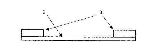
表1に示すように、従来の形状のスティフナーでは熱膨張係数の大きな材質を用いても効果は無い。また従来用いられていた熱膨張係数の材質では本発明の形状にしても改善は見られなかった。一方、本発明の形状で,かつその熱膨張係数が本発明に係る材質のものにした場合、変動量は小さく押さえられ、本発明のスティフナーを用いることで多層回路配線板の変形を抑えることが可能であることが確認された。
【0019】
なお上記実施形態は本発明の実施形態の一例に過ぎず、本発明は上記実施形態に限定されるものではない。
【0020】
【発明の効果】
以上説明したように、本発明のスティフナー付き多層回路配線板を用いることにより、ローカルリフロー方式のハンダリフロー工程においてスティフナーで固定した多層回路配線板の熱変形を最小にすることが可能となり、熱変形によって引き起こされる半導体素子と多層回路配線板との接続不良を減少できる。
【0021】
【図面の簡単な説明】
【図1】本発明のスティフナー付き多層回路配線板を示す断面図
【図2】本発明のスティフナー付き多層回路配線板のスティフナーの一例を示す説明図
【図3】従来の形状のスティフナーと多層回路配線板を接着した状態を示す断面図
【符号の説明】
1・・・多層回路配線板
2・・・スティフナー
3・・・スティフナー
4・・・窪み[0001]
BACKGROUND OF THE INVENTION
The present invention relates to a multilayer circuit wiring board with a stiffener having a multilayer circuit wiring board on which a semiconductor element is mounted and a stiffener for holding the multilayer circuit wiring board when the semiconductor element is connected to the multilayer circuit wiring board. Relates to a multilayer circuit wiring board with a stiffener that can improve a connection failure in a solder reflow process, which is one of the processes when connecting a semiconductor element to a multilayer circuit wiring board, and in particular, a system called a local reflow system.
[0002]
[Prior art]
In recent years, semiconductor devices such as semiconductor large-scale integrated circuits (LSIs) whose operating speed reaches 1 GHz in clock frequency have appeared. In such a high-speed semiconductor, the degree of integration of transistors is high, and as a result, the number of input / output terminals may exceed 1000.
In order to mount such a multi-terminal semiconductor element on a printed wiring board, a multilayer circuit wiring board is arranged between the semiconductor element and the printed board and relays electrical connection between them. The multilayer circuit wiring board has a very thin layer structure and a wiring pattern having a finer wiring pitch than the printed wiring board in order to cope with bonding with terminals of highly dense semiconductor elements. Also, solder bumps are provided at the contact portions for bonding with the semiconductor elements. Examples of multilayer circuit wiring boards that are currently in wide use include BGA (Ball Grid Array) and CSP (Chip Size Package).
[0003]
Recently, for higher density mounting and higher operating frequency, polyimide resin films and other layers with wiring patterns are laminated to reduce the overall thickness of the multilayer circuit wiring board and increase the interlayer sustain length. Some products have been developed that can be made shorter to cope with higher operating frequencies.
[0004]
There are several methods for mounting semiconductor elements on a multilayer circuit wiring board, but a solder reflow apparatus is generally used. In this apparatus, the temperature is raised to around 260 ° C. while being transported through the apparatus with the semiconductor element and the multilayer circuit wiring board being precisely aligned, and then returned to room temperature. As described above, the solder bumps provided for bonding are melted at a high temperature, and the predetermined portions of the multilayer circuit wiring board and the semiconductor element are bonded to each other.
[0005]
Multi-layer circuit wiring boards are formed by laminating polyimide resin films, etc. to form a wiring pattern. They are thin and easy to bend and become unstable when mounting semiconductor elements. Flattening is performed by bonding a metal plate called a stiffener having a shape surrounding a semiconductor element mounting portion at the outer edge. When a polyimide resin film is used for the multilayer circuit wiring board, for example, copper is generally used as the stiffener material. This is because polyimide resin and copper have substantially the same thermal expansion coefficient, and it is considered that there is little problem with temperature change in the solder reflow process and there is no problem.
[0006]
In addition, as a conventional technique related to the shape of the stiffener, in order to ensure the joining of solder balls provided for joining the multilayer wiring board and the mounting board when the multilayer wiring board on which the semiconductor element is mounted is joined to the mounting board. In order to relieve the stress between the constituent elements, a stiffener is formed at a position immediately above the solder ball so as to form a space. (For example, see Patent Document 1)
[0007]
[Patent Document 1]
Japanese Patent Laid-Open No. 11-220055 (
[0008]
[Problems to be solved by the invention]
However, the terminals of semiconductor elements have become increasingly dense in recent years. In particular, the solder bumps for connecting the semiconductor elements and the multilayer circuit wiring board, which is a multilayer wiring board, are very small. Displacement in the inside and poor bonding have been a major problem. In particular, this slight deformation becomes a problem in the so-called local reflow type solder reflow process in which heating is performed from one side, usually from the lower side, even in the solder reflow process.
[0009]
The cause of the positional deviation during the process is considered as follows. In order to attach the semiconductor element to the central portion of the multilayer circuit wiring board, the stiffener has a frame shape surrounding the semiconductor element and has a through hole in the central portion. Therefore, the stiffener is bonded to the multilayer circuit wiring board at its peripheral portion. When heated from the side of the multilayer circuit wiring board, which is the lower surface, in the solder reflow system using the local reflow method, a temperature difference occurs between the multilayer circuit wiring board and the stiffener, and the multilayer circuit wiring board is made of polyimide resin as described above. Even if the stiffener is made of copper and the thermal expansion coefficients are made equal, a difference in expansion occurs.
[0010]
In this way, the multilayer circuit wiring board has a higher temperature than the stiffener, so the expansion is greater, but the peripheral part is bonded to the metal stiffener, so the area where the semiconductor elements of the multilayer circuit wiring board are mounted A slack is generated, the flat state cannot be maintained, and it swells up and down. As a result, when it swells to the semiconductor element side, the solder bump melted at a high temperature is crushed, and when it is separated from the semiconductor element, the bonding by the solder bump may not be formed or the bonding may become unstable. .
[0011]
The present invention has been made in view of the above circumstances, and the object thereof is a solder reflow process performed for connecting a semiconductor element to a multilayer circuit wiring board, particularly in a local reflow solder reflow process. An object of the present invention is to provide a multilayer circuit wiring board with a stiffener capable of maintaining the flatness of the multilayer circuit wiring board and ensuring the connection between the semiconductor element and the multilayer circuit wiring board.
[0012]
[Means for Solving the Problems]
In order to achieve the above object, the present invention takes the following measures.
That is, the shape of the stiffener of the present invention is a frame body whose outer edge is positioned outside the outer edge of the multilayer circuit wiring board to which the outer edge is bonded, and whose inner edge is positioned inside the multilayer circuit wiring board, and the multilayer circuit wiring on the lower surface. It has a recess with a depth equivalent to the thickness of the plate. The stiffener is made of a metal having a thermal expansion coefficient that is 15% to 30% larger than that of the multilayer circuit wiring board. The multilayer circuit wiring board is bonded to the recess so as to be fitted.
[0013]
When a multi-layer circuit wiring board is bonded to such a stiffener in a local reflow solder reflow apparatus, the lower surface of the multilayer circuit wiring board is substantially flush with the lower surface of the stiffener, and part of the lower surface of the stiffener is Because it is exposed to the heating surface, the temperature difference between the multilayer circuit wiring board and the stiffener can be reduced, and the coefficient of thermal expansion of the stiffener is made larger than that of the multilayer circuit wiring board to increase the elongation of the stiffener. A tension in the surface direction is applied to the circuit wiring board to make it difficult for sagging to occur and suppress deviation from a flat state. The value of the coefficient of thermal expansion of the stiffener is desirably 15% to 30% larger than that of the multilayer circuit wiring board. Here, when the coefficient of thermal expansion of the stiffener is less than 15% compared to the multilayer circuit wiring board, the effect of reducing the sag is poor, and when it is more than 30%, the difference in elongation becomes too large and the positional deviation is excessive. It can happen.
[0014]
DETAILED DESCRIPTION OF THE INVENTION
In the following, an embodiment of a stiffener capable of more reliably performing a solder reflow process for connecting a semiconductor element and a multilayer circuit wiring board according to the present invention will be described in more detail with reference to the drawings. .
[0015]
FIG. 1 is an explanatory diagram of a cross-sectional shape of a
[0016]
For the embodiment of FIG. 1 and the conventional one of FIG. 3 for comparison, the stiffener is made of copper having the same thermal expansion coefficient as that of the multilayer circuit wiring board, and brass having a 20% higher thermal expansion coefficient than copper. It created with two types of materials and compared about each combination. Here, the linear expansion coefficient of copper is 16.5 [10 −6 / K], and the linear expansion coefficient of brass is 19.8 [10 −6 / K]. The linear expansion coefficient of polyimide, which is the base material of the multilayer circuit wiring board, is equivalent to copper. The multilayer circuit wiring board was heated from the bonded side, heated to 260 ° C. in about 100 seconds, held for 30 seconds, and returned to room temperature in about 50 seconds. Table 1 shows the results of measuring the amount of change in the vertical direction of the region where the semiconductor elements are joined at the center of the multilayer circuit wiring board at this time.
[0017]
[Table 1]
As shown in Table 1, the conventional stiffener has no effect even if a material having a large thermal expansion coefficient is used. Further, the material having a thermal expansion coefficient that has been conventionally used has not been improved even in the shape of the present invention. On the other hand, when the shape of the present invention is used and the thermal expansion coefficient is made of the material according to the present invention, the amount of variation is suppressed to a small extent, and the deformation of the multilayer circuit wiring board can be suppressed by using the stiffener of the present invention. It was confirmed that it was possible.
[0019]
In addition, the said embodiment is only an example of embodiment of this invention, and this invention is not limited to the said embodiment.
[0020]
【The invention's effect】
As described above, by using the multilayer circuit wiring board with a stiffener of the present invention, it becomes possible to minimize the thermal deformation of the multilayer circuit wiring board fixed by the stiffener in the local reflow type solder reflow process. Connection failure between the semiconductor element and the multilayer circuit wiring board caused by the above can be reduced.
[0021]
[Brief description of the drawings]
[1] stiffener with multilayer circuit diagram showing an example of a stiffener of the stiffener with the multilayer circuit wiring board of a cross-sectional view Figure 2 the invention showing a
1 ... Multilayer circuit board
2 ... Stiffener
3.Stiffener
4 ... depression
Claims (1)
Priority Applications (1)
| Application Number | Priority Date | Filing Date | Title |
|---|---|---|---|
| JP2003148684A JP4333218B2 (en) | 2003-05-27 | 2003-05-27 | Multi-layer circuit board with stiffener |
Applications Claiming Priority (1)
| Application Number | Priority Date | Filing Date | Title |
|---|---|---|---|
| JP2003148684A JP4333218B2 (en) | 2003-05-27 | 2003-05-27 | Multi-layer circuit board with stiffener |
Publications (2)
| Publication Number | Publication Date |
|---|---|
| JP2004356142A JP2004356142A (en) | 2004-12-16 |
| JP4333218B2 true JP4333218B2 (en) | 2009-09-16 |
Family
ID=34044984
Family Applications (1)
| Application Number | Title | Priority Date | Filing Date |
|---|---|---|---|
| JP2003148684A Expired - Fee Related JP4333218B2 (en) | 2003-05-27 | 2003-05-27 | Multi-layer circuit board with stiffener |
Country Status (1)
| Country | Link |
|---|---|
| JP (1) | JP4333218B2 (en) |
Families Citing this family (3)
| Publication number | Priority date | Publication date | Assignee | Title |
|---|---|---|---|---|
| KR101013546B1 (en) * | 2007-08-31 | 2011-02-14 | 주식회사 하이닉스반도체 | Substrate used memory module |
| JP5306879B2 (en) * | 2009-03-30 | 2013-10-02 | 日本特殊陶業株式会社 | Reinforced wiring board |
| CN114236901B (en) * | 2017-03-31 | 2023-08-22 | 沪苏艾美珈光学技术(江苏)有限公司 | Light distribution control element, light distribution adjusting mechanism, reflecting member, reinforcing plate, illumination unit, display, and television |
-
2003
- 2003-05-27 JP JP2003148684A patent/JP4333218B2/en not_active Expired - Fee Related
Also Published As
| Publication number | Publication date |
|---|---|
| JP2004356142A (en) | 2004-12-16 |
Similar Documents
| Publication | Publication Date | Title |
|---|---|---|
| US8181342B2 (en) | Method for manufacturing a coreless packaging substrate | |
| KR100531393B1 (en) | Semiconductor device and manufacturing method of the same | |
| US6509529B2 (en) | Isolated flip chip of BGA to minimize interconnect stress due to thermal mismatch | |
| JP5088138B2 (en) | Mounting board and electronic equipment | |
| US20090301766A1 (en) | Printed circuit board including electronic component embedded therein and method of manufacturing the same | |
| US6317331B1 (en) | Wiring substrate with thermal insert | |
| JP2002190488A (en) | Method for manufacturing semiconductor device and the semiconductor device | |
| US8450825B2 (en) | Semiconductor package | |
| JPH03246993A (en) | Mounting board | |
| US7459796B2 (en) | BGA-type multilayer circuit wiring board | |
| US7253504B1 (en) | Integrated circuit package and method | |
| US7911048B2 (en) | Wiring substrate | |
| JP4333218B2 (en) | Multi-layer circuit board with stiffener | |
| JP2016025281A (en) | Semiconductor device and method for manufacturing the same | |
| KR100730763B1 (en) | Substrate with multi-layer interconnection structure and method of manufacturing the same | |
| JP2007299887A (en) | Substrate for mounting semiconductor integrated circuit element, and semiconductor device | |
| US20070257375A1 (en) | Increased interconnect density electronic package and method of fabrication | |
| JP2005340355A (en) | Wiring board | |
| TW437019B (en) | Improved wiring substrate with thermal insert | |
| JP2005123493A (en) | Wiring substrate and element packaging substrate | |
| JP5067107B2 (en) | Circuit board and semiconductor device | |
| JP4599891B2 (en) | Semiconductor device substrate and semiconductor device | |
| JP2011091091A (en) | Structure and method for mounting electronic component | |
| JP2002299387A (en) | Tape carrier for semiconductor device and its manufacturing method | |
| JP2007305653A (en) | Multilayer circuit wiring board and semiconductor device |
Legal Events
| Date | Code | Title | Description |
|---|---|---|---|
| A621 | Written request for application examination |
Free format text: JAPANESE INTERMEDIATE CODE: A621 Effective date: 20060320 |
|
| A131 | Notification of reasons for refusal |
Free format text: JAPANESE INTERMEDIATE CODE: A131 Effective date: 20090217 |
|
| A521 | Written amendment |
Free format text: JAPANESE INTERMEDIATE CODE: A523 Effective date: 20090416 |
|
| TRDD | Decision of grant or rejection written | ||
| A01 | Written decision to grant a patent or to grant a registration (utility model) |
Free format text: JAPANESE INTERMEDIATE CODE: A01 Effective date: 20090602 |
|
| A01 | Written decision to grant a patent or to grant a registration (utility model) |
Free format text: JAPANESE INTERMEDIATE CODE: A01 |
|
| A61 | First payment of annual fees (during grant procedure) |
Free format text: JAPANESE INTERMEDIATE CODE: A61 Effective date: 20090615 |
|
| FPAY | Renewal fee payment (event date is renewal date of database) |
Free format text: PAYMENT UNTIL: 20120703 Year of fee payment: 3 |
|
| R150 | Certificate of patent or registration of utility model |
Free format text: JAPANESE INTERMEDIATE CODE: R150 |
|
| A521 | Written amendment |
Free format text: JAPANESE INTERMEDIATE CODE: A523 Effective date: 20090416 |
|
| FPAY | Renewal fee payment (event date is renewal date of database) |
Free format text: PAYMENT UNTIL: 20120703 Year of fee payment: 3 |
|
| FPAY | Renewal fee payment (event date is renewal date of database) |
Free format text: PAYMENT UNTIL: 20130703 Year of fee payment: 4 |
|
| FPAY | Renewal fee payment (event date is renewal date of database) |
Free format text: PAYMENT UNTIL: 20140703 Year of fee payment: 5 |
|
| LAPS | Cancellation because of no payment of annual fees |