EP2005439B1 - Program time adjustment as function of program voltage for improved programming speed - Google Patents
Program time adjustment as function of program voltage for improved programming speed Download PDFInfo
- Publication number
- EP2005439B1 EP2005439B1 EP07758602A EP07758602A EP2005439B1 EP 2005439 B1 EP2005439 B1 EP 2005439B1 EP 07758602 A EP07758602 A EP 07758602A EP 07758602 A EP07758602 A EP 07758602A EP 2005439 B1 EP2005439 B1 EP 2005439B1
- Authority
- EP
- European Patent Office
- Prior art keywords
- program
- pulses
- programming
- storage elements
- charge storage
- Prior art date
- Legal status (The legal status is an assumption and is not a legal conclusion. Google has not performed a legal analysis and makes no representation as to the accuracy of the status listed.)
- Not-in-force
Links
- 238000000034 method Methods 0.000 claims description 19
- 230000004044 response Effects 0.000 claims description 12
- 230000006870 function Effects 0.000 abstract description 6
- 238000010586 diagram Methods 0.000 description 10
- 238000007796 conventional method Methods 0.000 description 5
- 230000008569 process Effects 0.000 description 5
- 230000008901 benefit Effects 0.000 description 4
- 230000000694 effects Effects 0.000 description 3
- 230000001413 cellular effect Effects 0.000 description 1
- 230000008859 change Effects 0.000 description 1
- 238000004891 communication Methods 0.000 description 1
- 238000012986 modification Methods 0.000 description 1
- 230000004048 modification Effects 0.000 description 1
- 230000000737 periodic effect Effects 0.000 description 1
- 239000007787 solid Substances 0.000 description 1
Images


Classifications
-
- G—PHYSICS
- G11—INFORMATION STORAGE
- G11C—STATIC STORES
- G11C16/00—Erasable programmable read-only memories
- G11C16/02—Erasable programmable read-only memories electrically programmable
- G11C16/06—Auxiliary circuits, e.g. for writing into memory
- G11C16/34—Determination of programming status, e.g. threshold voltage, overprogramming or underprogramming, retention
-
- G—PHYSICS
- G11—INFORMATION STORAGE
- G11C—STATIC STORES
- G11C16/00—Erasable programmable read-only memories
- G11C16/02—Erasable programmable read-only memories electrically programmable
- G11C16/06—Auxiliary circuits, e.g. for writing into memory
- G11C16/10—Programming or data input circuits
-
- G—PHYSICS
- G11—INFORMATION STORAGE
- G11C—STATIC STORES
- G11C16/00—Erasable programmable read-only memories
- G11C16/02—Erasable programmable read-only memories electrically programmable
- G11C16/06—Auxiliary circuits, e.g. for writing into memory
- G11C16/32—Timing circuits
Definitions
- This invention relates in general to non-volatile memory systems and, in particular, to a non-volatile memory system with programming time control.
- the memory cells or charge storage elements (the two terms used herein interchangeably) of a non-volatile memory are typically programmed one partial or complete row of cells in parallel at a time.
- Programming voltage pulses are applied to the selected row of memory cells until the threshold voltage of each of the selected cells in the row has been programmed to a value within a predetermined voltage range (which may or may not be the final desired state of the cell) in a programming cycle.
- a time sequence of programming voltage pulses of voltage level or amplitude Vpgm are applied at predetermined time intervals, such as periodic time intervals, where the amplitude of each programming pulse has been incremented by a fixed voltage step ⁇ Vpgm (e.g. 0.2 V) compared to the amplitude of the immediately preceding programming pulse in the sequence.
- ⁇ Vpgm e.g. 0.2 V
- program-verify operations are carried out. That is, the programmed level of each charge storage element (e.g. charge storage transistor) being programmed in parallel is read after each programming pulse to determine whether it is not less than the verify voltage level to which it is being programmed. If it is determined that the threshold voltage of a given charge storage element has exceeded the verify voltage level, programming of such charge storage element is stopped by raising the voltage of the bit line to which the particular charge storage element is connected to from a low voltage (typically 0 volts) to a high or inhibit level (typically Vdd). Programming of other charge storage elements being programmed in parallel continues until they in turn reach their verify voltage levels.
- a low voltage typically 0 volts
- inhibit level typically Vdd
- the amplitude of the programming pulse is increased by the predetermined step size and applied again to the charge storage elements being programmed in parallel, which is followed again by a program-verify operation. If after the next programming operation the increased programming pulse still has not caused the threshold voltage of all of the charge storage elements being programmed in parallel to reach the verify voltage level, the amplitude of the programming pulse is increased yet again by the same predetermined step size during the next time interval and this process is repeated until threshold voltages of all of the charge storage elements being programmed in parallel have reached the verify voltage level. This marks the end of a particular programming cycle.
- the above programming process requires repetitively programming the cells with a programming pulse followed by a program-verify operation. This process, therefore, can be time consuming. It is, therefore, desirable for the program time for the application of each programming pulse to have a short duration so that the memory cells or charge storage elements can be programmed to the desired threshold voltages in as short a time as possible.
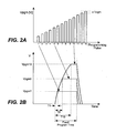
- the time sequence of programming pulses that are used to program charge storage elements is illustrated in Fig. 2A , where 13 such consecutive pulses are shown, although it is possible to employ a larger or fewer number of pulses for programming the elements to any particular threshold voltage.
- the voltage pulses may start at an initial program pulse level such as 15 volts and increase by a predetermined step size such as 0.2 volts for every pulse.
- Fig. 2A the programming pulses in the sequence used to program charge storage elements are illustrated to have substantially vertical leading and trailing edges.
- the pulse shape of the programming pulses is different from those shown, because a charge pump typically requires a charge-up time to increase the voltage output from a reference voltage level to the required Vpgm level, and the pulse requires a time period to decrease back to the reference level at the trailing edge of the pulse. This is illustrated in Figs. 1 and 2B .
- the charge pump starts increasing the voltage output from a starting reference level such as the ground level, and applies the output to the selected control gate line or word line. However, it is not until the time t1 that the output of the charge pump reaches the required voltage level Vpgm that is effective for altering transistor threshold voltage as shown in Fig. 1 . After the output of the charge pump reaches the required voltage level at time t1, this voltage level is maintained until a time t2 which marks the end of the time period in which the output of the charge pump is maintained at the required program voltage level Vpgm. Thereafter, the charge pump output declines back to the reference level by time t3.
- a starting reference level such as the ground level
- the total program time allocated for programming the control gate line or word line is the sum of two of the three time periods: t0-t1 (or T) and t1-t2, and the memory proceeds to the next program pulse or program verify after t3.
- the time period t0-t1 or T is the charge-up time required for the charge pump in order to deliver the required program voltage level Vpgm.
- the time period t1-t2 is the pulse width, which is the effective program time during which the voltage of the selected control gate line or word line is ramped up to the desired Vpgm level effective for altering the threshold voltage of charge storage elements.
- each of the 13 pulses labeled 1 through 13 actually has a shape similar to that shown in Fig. 1 .
- the Vpgm level that is required to be delivered by the charge pump increases by ⁇ Vpgm every time a new charge pump pulse is generated, so that the required program voltage or Vpgm level trends higher from pulse 1 to pulse 13 as shown in Fig. 2A .
- a higher Vpgm level requires a longer charge-up time compared to a lower Vpgm as illustrated in Fig. 2B .
- the Vpgm5 level that needs to be delivered by the charge pump is higher than that for pulse 1 so that a longer charge-up time T5 is required, leaving a shorter time available for applying the ramped up voltage at Vpgm5 level to the selected control gate line or word line effective for altering the threshold voltage of the charge storage elements controlled by such line.
- the required voltage pump pulse level Vpgm10 is even higher so that an even longer charge-up time T10 is required leaving an even smaller portion of the fixed program time available for the charge pump output at Vpgm10 for altering the threshold voltage of the charge storage elements.
- One solution to the above problem is to increase the fixed time allocated for the programming, so that even at high programming voltages, the increased program time allocated allows the charge pump output at the required high Vpgm level to stay at such level for an adequate time for altering charge storage element threshold voltages even after an increased charge-up time.
- the programming time of each programming cycle in which the programming pulses are applied it will be desirable to minimize the programming time of each programming cycle in which the programming pulses are applied. Since allocating a longer programming time is needed only at high programming voltages (i.e. at high Vpgm levels) but not at low programming voltages, increasing the fixed program time for the generation and application of all of the charge pump pulses during the programming cycle would also be undesirable since it also increases the total programming time. If is therefore desirable to provide a non-volatile memory system, where the above-described difficulties are alleviated.
- WO96/41346 discloses a memory and method according to the preambles of the independent claims.
- US 5,991,201 discloses a memory array in which the lengths of programming pulses applied to bit lines and word lines are changed during a sequence of programming pulses.
- a method for programming non-volatile memory system comprising a plurality of charge storage elements.
- the method comprising providing sequentially program pulses by means of a charge pump where the amplitude of each of at least some of the pulses increases relative to a prior pulse during a programming cycle for programming said plurality of charge storage elements.
- the method further comprises generating a plurality of program time control signals in response to signals indicative of different amplitudes of the pulses provided by the charge pump.
- the program time control signals cause program times allocated for application of the program pulses to the charge storage elements to be adjusted a plurality of times to values that cause the time during which the pulse voltage is maintained at a desired voltage following a charge up time of the charge pump to remain substantially constant so as to reduce the number of pulses for programming said plurality of charge storage elements to a predetermined state.
- a non-volatile memory system comprising a plurality of charge storage elements, a charge pump providing sequentially program pulses where the amplitude of each of at least some of the pulses increases relative to a prior pulse during a programming cycle for programming said plurality of charge storage elements and a device that generates a plurality of program time control signals in response to signals indicative of different amplitudes of the pulses provided by the charge pump.
- the program time control signals cause program times allocated for application of the program pulses to the charge storage elements to be adjusted a plurality of times to values that cause the time during which the pulse voltage is maintained at a desired voltage following a charge up time of the charge pump to remain substantially constant so as to reduce the number of pulses for programming said plurality of charge storage elements to a predetermined state.
- the program time period allocated is as short as possible during the beginning portion of the program cycle when the charge pump is called upon to supply low to moderate voltage outputs for the program pulses.
- the program time period allocated it is desirable for longer program time periods to be used instead of the shorter time period used initially.
- the program time allocated for the voltage pump pulses can be increased when the charge pump is called upon to supply high voltage output for the program pulses.
- the program time allocated for application of the voltage pump pulses is adjusted a plurality of times to values that reduce the number of pulses for programming the charge storage elements to a predetermined state (i.e. a state where the elements are within a predetermined range of threshold voltages).
- the program time allocated is controlled as a function of the number of program pulses that have been generated by the charge pump during a particular programming cycle.
- the program time allocated is controlled as a function of the amplitude or amplitudes of pulses provided by the charge pump without using any output of the charge pump.
- At least one program time allocated for application of the voltage pump pulses is generated in response to at least one indicator signal indicative of the amplitude or amplitudes of pulses provided by the charge pump.
- the indicator signal or signals are being generated without using amplitude of any output of the charge pump.
- the indicator signal or signals are provided by a program voltage control logic which also controls the voltage level of the pump pulses provided by the charge pump, and which controls the program time allocated.
- the indicator signal or signals are indicative of the number of program pulses that have been generated by the charge pump during a particular programming cycle.
- Fig. 1 is a timing diagram of a voltage pump pulse generated by a charge pump useful for illustrating an aspect of the invention.
- Fig. 2A is a timing diagram of a time sequence of 13 voltage pump pulses at increasing voltage (Vpgm) levels useful for illustrating an aspect of the invention.
- Fig. 2B is a timing diagram of three voltage pump pulses illustrating the fact that voltage pump pulse at a higher voltage level requires a longer charge-up time, useful for illustrating an aspect of the invention.
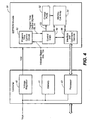
- Fig. 3 illustrates a block diagram of a system including a host device and a flash EEPROM system connected to the host device.
- Fig. 4 is a block diagram of the controller and voltage generation portion of the flash EEPROM system of Fig. 3 to illustrate one embodiment of the invention.
- Fig. 5 is a schematic circuit diagram of the program time control circuit and some components of the control logic in Fig. 4 to illustrate an embodiment of the invention.
- Fig. 6 is a schematic circuit diagram of the program time control circuit and some components of the control logic in Fig. 4 to illustrate another embodiment of the invention.
- Fig. 7 is a graphical plot of the target threshold voltage Vt of charge storage elements plotted against the number of voltage pump pulses required to program a NAND cell so that the cell reaches the target threshold voltage Vt.
- the dotted line with positive slope indicates the programming speed at constant pulse width (i.e. constant effective program time) and the solid curve indicates the programming speed at constant program time allocated for programming.
- Fig. 8 is a graphical plot of three voltage pump pulses at different voltage levels but with the same pulse width useful to illustrate embodiments of the invention.
- Fig. 9 is a graphical plot of the threshold voltages achieved with three different options for increasing the program time as a function of the required program voltage to illustrate embodiments of the invention.
- FIG. 3 is a block diagram of a flash memory system 20 (which can be in the form of a plug-in card or module) in communication with a host device 10 (e.g. computer, camera, cellular phone, personal digital assistant, game controllers, and media players such as MP3 players) through system bus 15.
- the flash memory system 20 includes a flash EEPROM module 30 and a controller 40, which includes, in turn, memory 41 and a processor 43. Controller 40 interprets the commands received from the host computer 10 and translates them into corresponding read, write and other operations for the flash EEPROM module 30, in a manner transparent to the host computer 10.
- FIG. 4 illustrates, as an example, a simplified block diagram of portions of the flash EEPROM system 20 related to the generation of the charge pump voltage pulses.
- the terms “voltage pump pulses”, “pump pulses”, “charge pump voltage pulses”, “programming pulses” and “program pulses” are used interchangeably.
- the supply voltage Vsys is applied by the host 10 to controller 40 and through an optional voltage regulator 45; a possibly different voltage level, Vdd, is applied to module 30.
- Processor 43 applies commands and data to module 30 and the charge pump 32 generates the programming pulses from the voltage Vdd in response to the control signals from control logic 58.
- Control logic 58 In practice there is usually sufficient logic in the control logic 58 in the non-volatile memory 30 to control the detailed operation of the memory, relieving Processor 43 from this responsibility.
- Decode Module 56 consists of sufficient logic to interpret commands from Processor 43 using a pre-defined protocol
- Control Logic 58 consists of a dedicated sequencer, a pulse counter and a Vpgm control logic, possibly with some parameters stored in a separate ROM (not shown) within Array 54 and read out upon startup.
- the pulse counter in Control Logic 58 is reset to 0 at the beginning of each programming cycle and counts starting from 0 the number of program pulses launched by the sequencer.
- the Sequencer uses the pulse count output of the pulse counter, the Sequencer decides from which loop it starts program verifies and/or at which loop it terminates the program loop with a program fail status.
- the Vpgm control logic in Control Logic 58 calculates Vpgm level of each program pulse.
- the programming pulses are applied to a memory cell array 54.
- Array 54 comprises rows and columns of memory cells. For simplicity in description, the various control circuits for row and column control, as well as other controls, for the memory array have been omitted from FIG. 4 .
- Circuit 52 controls the programming time of the pulses generated by the charge pump 32 as a function of an indicator signal from control logic 58 indicating the amplitude of the pulses.
- the program time control circuit 52 generates program time control signals 66 or 74 and supplies such signals to Control Logic 58 to cause the program times allocated for application of the voltage pump pulses from the charge pump 32 to the charge storage elements in array 54 to be adjusted to reduce the number of pulses required for programming the charge storage elements to a predetermined charge state, such as to program charge storage transistors to threshold voltages within a certain predetermined range.
- These program time control signals are supplied to Control Logic 58 for controlling the length of program time allocated for application of the voltage pump pulses to array 54.
- Fig. 5 is a schematic circuit diagram of one embodiment of the program time control scheme of Fig. 4 .
- Circuit 52' is one implementation of circuit 52 of Fig. 4 .
- Pulse counter 64 and sequencer 68 are parts of the control logic 58 of Fig. 4 .
- the pulse counter 64 in logic 58 resets to 0 at the beginning of each programming cycle and counts starting from 0 the number of program pulses launched by the sequencer.
- the pulse counter 64 outputs a pulse count signal 64a indicating the program pulse count from the beginning of such programming cycle.
- This pulse count signal is supplied to the program time control logic circuit 52' which may comprise logic circuits that implement a lookup table. This lookup table provides a value of program time corresponding to the pulse count number from counter 64.
- the charge pump increases the voltage level of the programming pulse by a voltage increment ⁇ Vpgm above the voltage level of the immediately preceding programming pulse, so that if the total number of programming pulses that have been provided during a particular programming cycle is known, the desired Vpgm level can be calculated from such number. From Fig. 1 and the discussion in reference thereto above, it is clear that for any given programming voltage level Vpgm desired, there is a corresponding value for the sum of charge-up time (t0-t1) plus the desired effective program time or pulse width (t1-t2), and that the higher the desired Vpgm value, the larger will be the charge-up time (t0-t1).
- the corresponding program time is increased by corresponding amounts, which can be obtained by means of calculation or calibration.
- the program time corresponding to any value of Vpgm it is then possible to arrive at a set of program times corresponding to a set of Vpgm values, and therefore also a set of corresponding pulse count values, so as to maintain a substantially constant effective program time (or pulse width) during which the program voltage is maintained at the desired Vpgm for different Vpgm and pulse count values.
- Fig. 7 is a graphical plot of the threshold voltage (on the vertical axis) of the charge storage elements that is achieved by the application of a corresponding number (on the horizontal axis) of voltage pump pulses in the sequence of pulse programming pulses such as those illustrated in Fig. 2A .
- the target threshold voltage Vt for a particular charge state to be achieved is shown as a horizontal dotted line 82.
- the dotted slanted line 84 illustrates the threshold voltage of the charge storage elements that can be achieved where the pulse width or effective program time (during which the pulse voltage is maintained at the desired program voltage) is maintained at a constant value as the program voltage Vpgm is increased so as to achieve an optimum programming speed.
- the threshold voltage of the charge storage elements that can be achieved corresponding to the number of pulses is shown as the solid line curve 86.
- line 82 intersects curve 86 at a point to the right of its intersection with line 84, indicating that the programming speed achieved with a constant program time allocation requires the application of many more programming pulses and is thus slower compared to one where the effective program time or pulse width is maintained constant.
- Fig. 8 is a graphical plot of three different programming pulses at three different values of Vpgm.
- Vpgm the required program voltage level
- Fig. 8 the amount of program time allocated is also increased correspondingly, so that the effective program time or pulse width remains substantially constant. This allows the optimum programming speed to be achieved, using the fewest number of programming pulses to cause charge storage elements to reach the target threshold voltage Vt, along the dotted line 84 in Fig. 7 .
- the optimum programming speed is achieved when the program time allocated for application of the voltage pump pulse is increased every time the amplitude of the pulse is increased as illustrated by line 84 in Figs. 7 and 9 , and labeled option 1 in Fig. 9 .
- the effective pulse width of the programming pulses can be maintained substantially constant to achieve the optimum programming speed.
- the program time allocated for the application of the voltage pump pulses is maintained at a constant value until Y number of pump pulses have been applied in the programming cycle.
- the threshold voltage that can be achieved is the same in option 3 and in curve 86 obtained in conventional methods of Fig. 7 .
- the curve 94 of option 3 diverges from curve 86 so that the total number of pulses required to achieve the target threshold Vt is reduced as compared to conventional methods as illustrated in Fig. 9 .
- curve 94 intersects the horizontal line 82 at a point closer to the vertical axis compared to where curve 86 intersects line 82.
- program time allocated may be increased each time the programming voltage is increased (such as after the application of every pulse) only after Y number of pulses have been applied, but not before this happens.
- This option is therefore a combination of prior options 1 and 3.
- the threshold voltage versus number of pulses plot for such combination will be along curve 86 of the conventional methods up to the point until Y number of pulses have been applied to the charge storage transistors, but along a line (not shown) that has substantially the same slope as line 84 in Fig. 9 after such point.
- the charge-up time may not be significant when the Vpgm level is relatively low, the effect of increasing the program time for such Vpgm levels after every program pulse is not as significant, so that there is not a big gain in programming efficiency by increasing the program time over conventional methods as illustrated by curve 86 in Figs. 7 and 9 .
- the desired Vpgm level is relatively high, the effect of increasing the program time for such Vpgm levels after every program pulse will be significant.
- By increasing the program time for such Vpgm levels after every program pulse only after Y number of pulses have been applied will achieve a significant gain in programming efficiency, while reducing the number of times the program time is adjusted.
- program time allocated may be increased, after Y number of pump pulses have been applied but not before this happens, each time X number of the programming pulses have been applied, where X is an integer equal to or greater than 2.
- This option is therefore a combination of prior options 2 and 3.
- This option has advantages similar to those when options 1 and 3 are combined, but has the additional advantage that the number of program time adjustments is further reduced.
- the threshold voltage versus number of pulses plot for such combination will be along curve 86 of the conventional methods up to the point until Y number of pulses have been applied to the charge storage transistors, but along a curve (not shown) that is of substantially the same shape and slope as curve 92 in Fig. 9 after such point.
- Circuit 52" of Fig. 6 is another embodiment of circuit 52 of Fig. 4 .
- the embodiment of Fig. 6 includes a program control logic 72 (in logic circuit 58 of Fig. 4 ) which provides the program voltage level (Vpgm level) in an indicator signal 72a to the program time control logic 52". Similar to program time control logic 52' of Fig. 5 , program time control logic 52" also implements a lookup table.
- Logic 52" provides a program time control signal 74 which indicates a program time corresponding to the input Vpgm level 72a.
- This program control time signal 74 is provided to sequencer 68 (in logic circuit 58 of Fig. 4 ) which provides such signal to the charge pump 32 along line 53.
- Logic 72 also provides the same Vpgm level signal 72a to charge pump 32 along signal line 98 (not shown in Fig. 4 ), so that the charge pump generates a voltage pump pulse with such Vpgm voltage level.
- Circuit 52" can also be used to implement the three different options illustrated in Fig. 9 , except that instead of increasing the program time after the application of one or more pulses, the program time is increased according to the Vpgm level called for by logic 72. In one implementation of the embodiment of Fig. 6 , the program time is increased for every n incremental increases (i.e.
- n is an integer equal to or greater than 1.
- the programming speed will be the same as the case where the program time is increased after every pump pulse, that is, along line 84 in Figs. 7 and 9 .
- n is of a value greater than 1
- the programming speed will be the same as the case where the program time is increased after every n pump pulses, that is, along dotted 92 in Fig. 9 .
- the program time is increased only once after m incremental increases, the result is illustrated also by option 3 and line 94 in Fig. 9 .
- the program time may be increased for every n incremental increases (i.e. n ⁇ Vpgm), where n is an integer equal to or greater than 1, but only after Y incremental increases, and not before this happens.
- n is of the value 1
- the programming speed will be the same as the case where options 1 and 3 are combined above for the embodiment of Fig. 5 .
- n is of a value greater than 1, the programming speed will be the same as the case where options 2 and 3 are combined above for the embodiment of Fig. 5 .
- the program time is increased at certain values of Vpgm, where these values may be selected to optimize the system, and may correspond to the options 1-3 and combinations thereof as explained above.
- the program time can be increased every time Vpgm is increased.
- the program time is set to values corresponding to certain values of Vpgm, where these values may correspond to every X number of pulses in option 2.
- the program time may be set to values corresponding to certain values of Vpgm, where these values do not correspond to every X number of pulses in option 2.
- the program time may be held constant in the programming cycle until the Vpgm exceeds a particular predetermined value, at which point the program time is increased to another value which stays unchanged until the end of the programming cycle.
Landscapes
- Read Only Memory (AREA)
- Non-Volatile Memory (AREA)
Applications Claiming Priority (3)
| Application Number | Priority Date | Filing Date | Title |
|---|---|---|---|
| US11/392,265 US7327608B2 (en) | 2006-03-28 | 2006-03-28 | Program time adjustment as function of program voltage for improved programming speed in programming method |
| US11/391,811 US7330373B2 (en) | 2006-03-28 | 2006-03-28 | Program time adjustment as function of program voltage for improved programming speed in memory system |
| PCT/US2007/064064 WO2007112213A2 (en) | 2006-03-28 | 2007-03-15 | Program time adjustment as function of program voltage for improved programming speed |
Publications (2)
| Publication Number | Publication Date |
|---|---|
| EP2005439A2 EP2005439A2 (en) | 2008-12-24 |
| EP2005439B1 true EP2005439B1 (en) | 2011-06-29 |
Family
ID=38541790
Family Applications (1)
| Application Number | Title | Priority Date | Filing Date |
|---|---|---|---|
| EP07758602A Not-in-force EP2005439B1 (en) | 2006-03-28 | 2007-03-15 | Program time adjustment as function of program voltage for improved programming speed |
Country Status (6)
| Country | Link |
|---|---|
| EP (1) | EP2005439B1 (enExample) |
| JP (1) | JP4669065B2 (enExample) |
| KR (1) | KR101312503B1 (enExample) |
| AT (1) | ATE515035T1 (enExample) |
| TW (1) | TWI340389B (enExample) |
| WO (1) | WO2007112213A2 (enExample) |
Families Citing this family (3)
| Publication number | Priority date | Publication date | Assignee | Title |
|---|---|---|---|---|
| US7330373B2 (en) | 2006-03-28 | 2008-02-12 | Sandisk Corporation | Program time adjustment as function of program voltage for improved programming speed in memory system |
| KR101893864B1 (ko) * | 2012-02-06 | 2018-08-31 | 에스케이하이닉스 주식회사 | 비휘발성 메모리 장치 및 프로그램 방법과 이를 이용하는 데이터 처리 시스템 |
| US11694751B2 (en) * | 2019-11-30 | 2023-07-04 | Semibrain Inc. | Logic compatible flash memory programming with a pulse width control scheme |
Family Cites Families (5)
| Publication number | Priority date | Publication date | Assignee | Title |
|---|---|---|---|---|
| EP0830684B1 (en) * | 1995-06-07 | 2004-08-25 | Macronix International Co., Ltd. | Automatic programming algorithm for page mode flash memory with variable programming pulse height and pulse width |
| US5991201A (en) * | 1998-04-27 | 1999-11-23 | Motorola Inc. | Non-volatile memory with over-program protection and method therefor |
| JP4170682B2 (ja) * | 2002-06-18 | 2008-10-22 | 株式会社東芝 | 不揮発性半導体メモリ装置 |
| US7110298B2 (en) * | 2004-07-20 | 2006-09-19 | Sandisk Corporation | Non-volatile system with program time control |
| JP2007115359A (ja) * | 2005-10-21 | 2007-05-10 | Oki Electric Ind Co Ltd | 半導体メモリのデータ書込方法 |
-
2007
- 2007-03-15 AT AT07758602T patent/ATE515035T1/de not_active IP Right Cessation
- 2007-03-15 EP EP07758602A patent/EP2005439B1/en not_active Not-in-force
- 2007-03-15 JP JP2009503138A patent/JP4669065B2/ja not_active Expired - Fee Related
- 2007-03-15 KR KR1020087025529A patent/KR101312503B1/ko not_active Expired - Fee Related
- 2007-03-15 WO PCT/US2007/064064 patent/WO2007112213A2/en not_active Ceased
- 2007-03-23 TW TW096110183A patent/TWI340389B/zh not_active IP Right Cessation
Also Published As
| Publication number | Publication date |
|---|---|
| KR20090018027A (ko) | 2009-02-19 |
| WO2007112213A2 (en) | 2007-10-04 |
| ATE515035T1 (de) | 2011-07-15 |
| KR101312503B1 (ko) | 2013-10-16 |
| TWI340389B (en) | 2011-04-11 |
| JP4669065B2 (ja) | 2011-04-13 |
| TW200805384A (en) | 2008-01-16 |
| JP2009531806A (ja) | 2009-09-03 |
| EP2005439A2 (en) | 2008-12-24 |
| WO2007112213A3 (en) | 2008-03-27 |
Similar Documents
| Publication | Publication Date | Title |
|---|---|---|
| US7675780B2 (en) | Program time adjustment as function of program voltage for improved programming speed in memory system | |
| CN101031978B (zh) | 具有编程时间控制的非易失性存储器系统 | |
| CN101421796B (zh) | 用于改进编程速度的依据编程电压的编程时间调节 | |
| US7551487B2 (en) | Nonvolatile memory device and related programming method | |
| JP4975310B2 (ja) | リップルフリー高電圧発生回路及び方法、及びこれを具備した半導体メモリ装置 | |
| US9437264B2 (en) | Memory operation latency control | |
| KR101212739B1 (ko) | 비휘발성 메모리장치 및 이의 동작방법 | |
| KR101003878B1 (ko) | 불휘발성 메모리 장치의 동작 방법 | |
| US11074979B2 (en) | Erase control circuit and method of non-volatile semiconductor memory device, and non-volatile semiconductor memory device | |
| EP2005439B1 (en) | Program time adjustment as function of program voltage for improved programming speed | |
| US20200381053A1 (en) | Non-volatile memory and operating method thereof | |
| EP3877979B1 (en) | Method of programming memory device | |
| US7187591B2 (en) | Memory device and method for erasing memory | |
| KR20070052403A (ko) | 낸드 플래시 메모리의 프로그램 방법 | |
| US12380955B2 (en) | Memory controller and method for adaptively programming flash memory | |
| KR20070035277A (ko) | 스텝형 컨버전스 프로그램 스킴을 구비한 플래시 메모리장치 |
Legal Events
| Date | Code | Title | Description |
|---|---|---|---|
| PUAI | Public reference made under article 153(3) epc to a published international application that has entered the european phase |
Free format text: ORIGINAL CODE: 0009012 |
|
| 17P | Request for examination filed |
Effective date: 20080929 |
|
| AK | Designated contracting states |
Kind code of ref document: A2 Designated state(s): AT BE BG CH CY CZ DE DK EE ES FI FR GB GR HU IE IS IT LI LT LU LV MC MT NL PL PT RO SE SI SK TR |
|
| 17Q | First examination report despatched |
Effective date: 20090204 |
|
| RIN1 | Information on inventor provided before grant (corrected) |
Inventor name: MIWA, TORU Inventor name: LEE, SHIH-CHUNG |
|
| GRAP | Despatch of communication of intention to grant a patent |
Free format text: ORIGINAL CODE: EPIDOSNIGR1 |
|
| DAX | Request for extension of the european patent (deleted) | ||
| GRAS | Grant fee paid |
Free format text: ORIGINAL CODE: EPIDOSNIGR3 |
|
| GRAA | (expected) grant |
Free format text: ORIGINAL CODE: 0009210 |
|
| AK | Designated contracting states |
Kind code of ref document: B1 Designated state(s): AT BE BG CH CY CZ DE DK EE ES FI FR GB GR HU IE IS IT LI LT LU LV MC MT NL PL PT RO SE SI SK TR |
|
| REG | Reference to a national code |
Ref country code: GB Ref legal event code: FG4D |
|
| REG | Reference to a national code |
Ref country code: CH Ref legal event code: EP |
|
| REG | Reference to a national code |
Ref country code: IE Ref legal event code: FG4D |
|
| REG | Reference to a national code |
Ref country code: DE Ref legal event code: R096 Ref document number: 602007015536 Country of ref document: DE Effective date: 20110825 |
|
| REG | Reference to a national code |
Ref country code: NL Ref legal event code: T3 |
|
| PG25 | Lapsed in a contracting state [announced via postgrant information from national office to epo] |
Ref country code: LT Free format text: LAPSE BECAUSE OF FAILURE TO SUBMIT A TRANSLATION OF THE DESCRIPTION OR TO PAY THE FEE WITHIN THE PRESCRIBED TIME-LIMIT Effective date: 20110629 Ref country code: SE Free format text: LAPSE BECAUSE OF FAILURE TO SUBMIT A TRANSLATION OF THE DESCRIPTION OR TO PAY THE FEE WITHIN THE PRESCRIBED TIME-LIMIT Effective date: 20110629 |
|
| PG25 | Lapsed in a contracting state [announced via postgrant information from national office to epo] |
Ref country code: AT Free format text: LAPSE BECAUSE OF FAILURE TO SUBMIT A TRANSLATION OF THE DESCRIPTION OR TO PAY THE FEE WITHIN THE PRESCRIBED TIME-LIMIT Effective date: 20110629 Ref country code: LV Free format text: LAPSE BECAUSE OF FAILURE TO SUBMIT A TRANSLATION OF THE DESCRIPTION OR TO PAY THE FEE WITHIN THE PRESCRIBED TIME-LIMIT Effective date: 20110629 Ref country code: SI Free format text: LAPSE BECAUSE OF FAILURE TO SUBMIT A TRANSLATION OF THE DESCRIPTION OR TO PAY THE FEE WITHIN THE PRESCRIBED TIME-LIMIT Effective date: 20110629 Ref country code: FI Free format text: LAPSE BECAUSE OF FAILURE TO SUBMIT A TRANSLATION OF THE DESCRIPTION OR TO PAY THE FEE WITHIN THE PRESCRIBED TIME-LIMIT Effective date: 20110629 Ref country code: GR Free format text: LAPSE BECAUSE OF FAILURE TO SUBMIT A TRANSLATION OF THE DESCRIPTION OR TO PAY THE FEE WITHIN THE PRESCRIBED TIME-LIMIT Effective date: 20110930 |
|
| PG25 | Lapsed in a contracting state [announced via postgrant information from national office to epo] |
Ref country code: BE Free format text: LAPSE BECAUSE OF FAILURE TO SUBMIT A TRANSLATION OF THE DESCRIPTION OR TO PAY THE FEE WITHIN THE PRESCRIBED TIME-LIMIT Effective date: 20110629 |
|
| PG25 | Lapsed in a contracting state [announced via postgrant information from national office to epo] |
Ref country code: IS Free format text: LAPSE BECAUSE OF FAILURE TO SUBMIT A TRANSLATION OF THE DESCRIPTION OR TO PAY THE FEE WITHIN THE PRESCRIBED TIME-LIMIT Effective date: 20111029 Ref country code: CZ Free format text: LAPSE BECAUSE OF FAILURE TO SUBMIT A TRANSLATION OF THE DESCRIPTION OR TO PAY THE FEE WITHIN THE PRESCRIBED TIME-LIMIT Effective date: 20110629 Ref country code: EE Free format text: LAPSE BECAUSE OF FAILURE TO SUBMIT A TRANSLATION OF THE DESCRIPTION OR TO PAY THE FEE WITHIN THE PRESCRIBED TIME-LIMIT Effective date: 20110629 Ref country code: PT Free format text: LAPSE BECAUSE OF FAILURE TO SUBMIT A TRANSLATION OF THE DESCRIPTION OR TO PAY THE FEE WITHIN THE PRESCRIBED TIME-LIMIT Effective date: 20111031 |
|
| PG25 | Lapsed in a contracting state [announced via postgrant information from national office to epo] |
Ref country code: RO Free format text: LAPSE BECAUSE OF FAILURE TO SUBMIT A TRANSLATION OF THE DESCRIPTION OR TO PAY THE FEE WITHIN THE PRESCRIBED TIME-LIMIT Effective date: 20110629 Ref country code: SK Free format text: LAPSE BECAUSE OF FAILURE TO SUBMIT A TRANSLATION OF THE DESCRIPTION OR TO PAY THE FEE WITHIN THE PRESCRIBED TIME-LIMIT Effective date: 20110629 Ref country code: PL Free format text: LAPSE BECAUSE OF FAILURE TO SUBMIT A TRANSLATION OF THE DESCRIPTION OR TO PAY THE FEE WITHIN THE PRESCRIBED TIME-LIMIT Effective date: 20110629 Ref country code: CY Free format text: LAPSE BECAUSE OF FAILURE TO SUBMIT A TRANSLATION OF THE DESCRIPTION OR TO PAY THE FEE WITHIN THE PRESCRIBED TIME-LIMIT Effective date: 20110629 |
|
| PLBE | No opposition filed within time limit |
Free format text: ORIGINAL CODE: 0009261 |
|
| STAA | Information on the status of an ep patent application or granted ep patent |
Free format text: STATUS: NO OPPOSITION FILED WITHIN TIME LIMIT |
|
| PG25 | Lapsed in a contracting state [announced via postgrant information from national office to epo] |
Ref country code: IT Free format text: LAPSE BECAUSE OF FAILURE TO SUBMIT A TRANSLATION OF THE DESCRIPTION OR TO PAY THE FEE WITHIN THE PRESCRIBED TIME-LIMIT Effective date: 20110629 |
|
| 26N | No opposition filed |
Effective date: 20120330 |
|
| PG25 | Lapsed in a contracting state [announced via postgrant information from national office to epo] |
Ref country code: DK Free format text: LAPSE BECAUSE OF FAILURE TO SUBMIT A TRANSLATION OF THE DESCRIPTION OR TO PAY THE FEE WITHIN THE PRESCRIBED TIME-LIMIT Effective date: 20110629 |
|
| REG | Reference to a national code |
Ref country code: DE Ref legal event code: R097 Ref document number: 602007015536 Country of ref document: DE Effective date: 20120330 |
|
| PG25 | Lapsed in a contracting state [announced via postgrant information from national office to epo] |
Ref country code: MC Free format text: LAPSE BECAUSE OF NON-PAYMENT OF DUE FEES Effective date: 20120331 |
|
| REG | Reference to a national code |
Ref country code: CH Ref legal event code: PL |
|
| REG | Reference to a national code |
Ref country code: IE Ref legal event code: MM4A |
|
| PG25 | Lapsed in a contracting state [announced via postgrant information from national office to epo] |
Ref country code: LI Free format text: LAPSE BECAUSE OF NON-PAYMENT OF DUE FEES Effective date: 20120331 Ref country code: IE Free format text: LAPSE BECAUSE OF NON-PAYMENT OF DUE FEES Effective date: 20120315 Ref country code: CH Free format text: LAPSE BECAUSE OF NON-PAYMENT OF DUE FEES Effective date: 20120331 |
|
| PG25 | Lapsed in a contracting state [announced via postgrant information from national office to epo] |
Ref country code: ES Free format text: LAPSE BECAUSE OF FAILURE TO SUBMIT A TRANSLATION OF THE DESCRIPTION OR TO PAY THE FEE WITHIN THE PRESCRIBED TIME-LIMIT Effective date: 20111010 |
|
| PGFP | Annual fee paid to national office [announced via postgrant information from national office to epo] |
Ref country code: FR Payment date: 20130325 Year of fee payment: 7 |
|
| PGFP | Annual fee paid to national office [announced via postgrant information from national office to epo] |
Ref country code: NL Payment date: 20130309 Year of fee payment: 7 |
|
| PG25 | Lapsed in a contracting state [announced via postgrant information from national office to epo] |
Ref country code: BG Free format text: LAPSE BECAUSE OF FAILURE TO SUBMIT A TRANSLATION OF THE DESCRIPTION OR TO PAY THE FEE WITHIN THE PRESCRIBED TIME-LIMIT Effective date: 20110929 |
|
| PG25 | Lapsed in a contracting state [announced via postgrant information from national office to epo] |
Ref country code: MT Free format text: LAPSE BECAUSE OF FAILURE TO SUBMIT A TRANSLATION OF THE DESCRIPTION OR TO PAY THE FEE WITHIN THE PRESCRIBED TIME-LIMIT Effective date: 20110629 |
|
| REG | Reference to a national code |
Ref country code: NL Ref legal event code: SD Effective date: 20131128 |
|
| REG | Reference to a national code |
Ref country code: DE Ref legal event code: R081 Ref document number: 602007015536 Country of ref document: DE Owner name: SANDISK TECHNOLOGIES INC., PLANO, US Free format text: FORMER OWNER: SANDISK CORPORATION, MILPITAS, CALIF., US Effective date: 20131212 Ref country code: DE Ref legal event code: R081 Ref document number: 602007015536 Country of ref document: DE Owner name: SANDISK TECHNOLOGIES LLC, PLANO, US Free format text: FORMER OWNER: SANDISK CORPORATION, MILPITAS, CALIF., US Effective date: 20131212 Ref country code: DE Ref legal event code: R081 Ref document number: 602007015536 Country of ref document: DE Owner name: SANDISK TECHNOLOGIES INC., US Free format text: FORMER OWNER: SANDISK CORPORATION, MILPITAS, US Effective date: 20131212 Ref country code: DE Ref legal event code: R082 Ref document number: 602007015536 Country of ref document: DE Representative=s name: MARKS & CLERK (LUXEMBOURG) LLP, LU Effective date: 20131212 |
|
| REG | Reference to a national code |
Ref country code: GB Ref legal event code: 732E Free format text: REGISTERED BETWEEN 20140206 AND 20140212 |
|
| REG | Reference to a national code |
Ref country code: FR Ref legal event code: TP Owner name: SANDISK TECHNOLOGIES INC., US Effective date: 20140225 |
|
| PG25 | Lapsed in a contracting state [announced via postgrant information from national office to epo] |
Ref country code: TR Free format text: LAPSE BECAUSE OF FAILURE TO SUBMIT A TRANSLATION OF THE DESCRIPTION OR TO PAY THE FEE WITHIN THE PRESCRIBED TIME-LIMIT Effective date: 20110629 |
|
| PG25 | Lapsed in a contracting state [announced via postgrant information from national office to epo] |
Ref country code: LU Free format text: LAPSE BECAUSE OF NON-PAYMENT OF DUE FEES Effective date: 20120315 |
|
| PG25 | Lapsed in a contracting state [announced via postgrant information from national office to epo] |
Ref country code: HU Free format text: LAPSE BECAUSE OF FAILURE TO SUBMIT A TRANSLATION OF THE DESCRIPTION OR TO PAY THE FEE WITHIN THE PRESCRIBED TIME-LIMIT Effective date: 20070315 |
|
| REG | Reference to a national code |
Ref country code: NL Ref legal event code: V1 Effective date: 20141001 |
|
| REG | Reference to a national code |
Ref country code: FR Ref legal event code: ST Effective date: 20141128 |
|
| PG25 | Lapsed in a contracting state [announced via postgrant information from national office to epo] |
Ref country code: FR Free format text: LAPSE BECAUSE OF NON-PAYMENT OF DUE FEES Effective date: 20140331 |
|
| PG25 | Lapsed in a contracting state [announced via postgrant information from national office to epo] |
Ref country code: NL Free format text: LAPSE BECAUSE OF NON-PAYMENT OF DUE FEES Effective date: 20141001 |
|
| REG | Reference to a national code |
Ref country code: DE Ref legal event code: R082 Ref document number: 602007015536 Country of ref document: DE Representative=s name: MARKS & CLERK (LUXEMBOURG) LLP, LU Ref country code: DE Ref legal event code: R081 Ref document number: 602007015536 Country of ref document: DE Owner name: SANDISK TECHNOLOGIES LLC, PLANO, US Free format text: FORMER OWNER: SANDISK TECHNOLOGIES INC., PLANO, TEX., US |
|
| PGFP | Annual fee paid to national office [announced via postgrant information from national office to epo] |
Ref country code: GB Payment date: 20180314 Year of fee payment: 12 |
|
| PGFP | Annual fee paid to national office [announced via postgrant information from national office to epo] |
Ref country code: DE Payment date: 20190305 Year of fee payment: 13 |
|
| GBPC | Gb: european patent ceased through non-payment of renewal fee |
Effective date: 20190315 |
|
| PG25 | Lapsed in a contracting state [announced via postgrant information from national office to epo] |
Ref country code: GB Free format text: LAPSE BECAUSE OF NON-PAYMENT OF DUE FEES Effective date: 20190315 |
|
| REG | Reference to a national code |
Ref country code: DE Ref legal event code: R119 Ref document number: 602007015536 Country of ref document: DE |
|
| PG25 | Lapsed in a contracting state [announced via postgrant information from national office to epo] |
Ref country code: DE Free format text: LAPSE BECAUSE OF NON-PAYMENT OF DUE FEES Effective date: 20201001 |