EP2005369B1 - Datenträger mit dehnungsmessung - Google Patents
Datenträger mit dehnungsmessung Download PDFInfo
- Publication number
- EP2005369B1 EP2005369B1 EP07735234A EP07735234A EP2005369B1 EP 2005369 B1 EP2005369 B1 EP 2005369B1 EP 07735234 A EP07735234 A EP 07735234A EP 07735234 A EP07735234 A EP 07735234A EP 2005369 B1 EP2005369 B1 EP 2005369B1
- Authority
- EP
- European Patent Office
- Prior art keywords
- data
- strain
- data carrier
- circuit
- substrate
- Prior art date
- Legal status (The legal status is an assumption and is not a legal conclusion. Google has not performed a legal analysis and makes no representation as to the accuracy of the status listed.)
- Active
Links
Images
Classifications
-
- G—PHYSICS
- G06—COMPUTING OR CALCULATING; COUNTING
- G06K—GRAPHICAL DATA READING; PRESENTATION OF DATA; RECORD CARRIERS; HANDLING RECORD CARRIERS
- G06K19/00—Record carriers for use with machines and with at least a part designed to carry digital markings
- G06K19/06—Record carriers for use with machines and with at least a part designed to carry digital markings characterised by the kind of the digital marking, e.g. shape, nature, code
- G06K19/067—Record carriers with conductive marks, printed circuits or semiconductor circuit elements, e.g. credit or identity cards also with resonating or responding marks without active components
- G06K19/07—Record carriers with conductive marks, printed circuits or semiconductor circuit elements, e.g. credit or identity cards also with resonating or responding marks without active components with integrated circuit chips
- G06K19/073—Special arrangements for circuits, e.g. for protecting identification code in memory
- G06K19/07309—Means for preventing undesired reading or writing from or onto record carriers
- G06K19/07345—Means for preventing undesired reading or writing from or onto record carriers by activating or deactivating at least a part of the circuit on the record carrier, e.g. ON/OFF switches
-
- G—PHYSICS
- G06—COMPUTING OR CALCULATING; COUNTING
- G06K—GRAPHICAL DATA READING; PRESENTATION OF DATA; RECORD CARRIERS; HANDLING RECORD CARRIERS
- G06K19/00—Record carriers for use with machines and with at least a part designed to carry digital markings
- G06K19/06—Record carriers for use with machines and with at least a part designed to carry digital markings characterised by the kind of the digital marking, e.g. shape, nature, code
- G06K19/067—Record carriers with conductive marks, printed circuits or semiconductor circuit elements, e.g. credit or identity cards also with resonating or responding marks without active components
- G06K19/07—Record carriers with conductive marks, printed circuits or semiconductor circuit elements, e.g. credit or identity cards also with resonating or responding marks without active components with integrated circuit chips
- G06K19/0716—Record carriers with conductive marks, printed circuits or semiconductor circuit elements, e.g. credit or identity cards also with resonating or responding marks without active components with integrated circuit chips at least one of the integrated circuit chips comprising a sensor or an interface to a sensor
- G06K19/0717—Record carriers with conductive marks, printed circuits or semiconductor circuit elements, e.g. credit or identity cards also with resonating or responding marks without active components with integrated circuit chips at least one of the integrated circuit chips comprising a sensor or an interface to a sensor the sensor being capable of sensing environmental conditions such as temperature history or pressure
-
- G—PHYSICS
- G06—COMPUTING OR CALCULATING; COUNTING
- G06K—GRAPHICAL DATA READING; PRESENTATION OF DATA; RECORD CARRIERS; HANDLING RECORD CARRIERS
- G06K19/00—Record carriers for use with machines and with at least a part designed to carry digital markings
- G06K19/06—Record carriers for use with machines and with at least a part designed to carry digital markings characterised by the kind of the digital marking, e.g. shape, nature, code
- G06K19/067—Record carriers with conductive marks, printed circuits or semiconductor circuit elements, e.g. credit or identity cards also with resonating or responding marks without active components
- G06K19/07—Record carriers with conductive marks, printed circuits or semiconductor circuit elements, e.g. credit or identity cards also with resonating or responding marks without active components with integrated circuit chips
- G06K19/0723—Record carriers with conductive marks, printed circuits or semiconductor circuit elements, e.g. credit or identity cards also with resonating or responding marks without active components with integrated circuit chips the record carrier comprising an arrangement for non-contact communication, e.g. wireless communication circuits on transponder cards, non-contact smart cards or RFIDs
-
- G—PHYSICS
- G06—COMPUTING OR CALCULATING; COUNTING
- G06K—GRAPHICAL DATA READING; PRESENTATION OF DATA; RECORD CARRIERS; HANDLING RECORD CARRIERS
- G06K19/00—Record carriers for use with machines and with at least a part designed to carry digital markings
- G06K19/06—Record carriers for use with machines and with at least a part designed to carry digital markings characterised by the kind of the digital marking, e.g. shape, nature, code
- G06K19/067—Record carriers with conductive marks, printed circuits or semiconductor circuit elements, e.g. credit or identity cards also with resonating or responding marks without active components
- G06K19/07—Record carriers with conductive marks, printed circuits or semiconductor circuit elements, e.g. credit or identity cards also with resonating or responding marks without active components with integrated circuit chips
- G06K19/073—Special arrangements for circuits, e.g. for protecting identification code in memory
- G06K19/07309—Means for preventing undesired reading or writing from or onto record carriers
- G06K19/07372—Means for preventing undesired reading or writing from or onto record carriers by detecting tampering with the circuit
- G06K19/07381—Means for preventing undesired reading or writing from or onto record carriers by detecting tampering with the circuit with deactivation or otherwise incapacitation of at least a part of the circuit upon detected tampering
-
- G—PHYSICS
- G06—COMPUTING OR CALCULATING; COUNTING
- G06K—GRAPHICAL DATA READING; PRESENTATION OF DATA; RECORD CARRIERS; HANDLING RECORD CARRIERS
- G06K7/00—Methods or arrangements for sensing record carriers, e.g. for reading patterns
- G06K7/0095—Testing the sensing arrangement, e.g. testing if a magnetic card reader, bar code reader, RFID interrogator or smart card reader functions properly
Definitions
- the invention relates to a data carrier comprising a data circuit arranged on a substrate and data transmission means being connected to the data circuit.
- RFID or contact data carriers are, for example, used for the identification of goods, documents, animals and persons, e.g. in passports, driver licences, ID cards, health cards, banking cards, animal ID tags, special company cards, security cards, and the like.
- RFID data carriers are employed to identify medical goods, e.g. medicines, injections, vaccines, etc.
- Data carriers that are used in said fields have a typical thickness of 380 ⁇ m and less (down to 30 ⁇ m and even below, dependent on the application and fab and grinding/etching/polishing technology), and there is a tendency to ever reduce the thickness of the data carriers. This means that the wafers for manufacturing the data carriers in form of integrated circuits are as thin as paper and are bendable and twistable.
- the substrates on which the ICs are defined often consist of flexible materials.
- bending and twisting, or in more general terms, exerting strains on the data carrier may cause malfunction of the data carrier or at least may result in operating the data carrier outside of its specification.
- the data tag comprises a data circuit that stores identification information, like personal data, health information, security access data, money values and the like.
- a plurality of antennae is coupled to the data circuit. At least one antenna of the plurality of antennae is a removable antenna capable of wireless signal transmission at a first range such that removal of the antenna substantially prevents communication of the identification information via the removed antenna and permits communication of the identification information via another antenna. "Removal" of the first antenna is carried out by switching a load-sensitive switch into the electric path between the data circuit and the first antenna. This implementation can for instance be used to create an orientation-sensitive RFID chip container.
- the data circuit is arranged at the body of a container, whereas the first antenna is arranged on a lid of the container.
- the lid is appropriately positioned on the body of the container, an electrical connection between the data circuit and the first antenna is maintained.
- the first antenna is physically disconnected from the data circuit, so that no wireless signals can be transmitted via the first antenna.
- a data carrier according to the invention comprises characteristic features, so that a data carrier according to the invention can be characterized in the way defined below, that is:
- a data carrier comprising a data circuit arranged on a substrate and data transmission means being connected to the data circuit, wherein the data carrier comprises at least one strain gauge means being adapted to measure strains exerted on the substrate and to transmit a deactivating signal to the data circuit if the measured strains exceed a defined strain threshold, the data circuit being adapted to interrupt data exchange with an external data reader/writer via the data transmission means, if it receives the deactivating signal.
- strain as used herein is defined as the amount of deformation of a body due to an applied force. More specifically, strain is defined as the fractional change in length. Strain can find its expression in tension, compression, warpage, bending and twisting of a body.
- the characteristic features according to the invention provide the advantage that the decision, whether or not a communication between the data carrier and an external data reader/writer is maintained in case of strain occurring on the data carrier, is taken by the logics of the data carrier, so that the data circuit has full control over this decision and is not dependent on external events like actuating a switch or breaking a conductor.
- This offers the opportunity to easily implement various operating modes of the data carriers on the occurrence of strains. For instance, it can be chosen whether the interruption of communication should be maintained temporarily or permanently. Further, logging of the occurrence of strains is an option.
- the solution of the present invention can also be used to test data circuits after they have been cut from a wafer.
- document US 6,906,514 B2 describes a system concept for decreasing or compensating influences of external disturbing quantities, such as, for example, mechanical stress in a semiconductor material, on the physical functional parameters of integrated circuits.
- external disturbing quantities such as, for example, mechanical stress in a semiconductor material
- the focus of attention of this system concept is not directed to potential damage by mechanical stress in the semiconductor material, but basically to the influence of physical parameters of the semiconductor material as a result of this mechanical stress which can, for instance, influence the electrical and magnetic characteristics of an integrated sensor assembly, such as a Hall sensor assembly.
- the mechanical stress in the semiconductor material is regarded as a type of excitation energy which has to be added to the energy balance in the semiconductor material.
- a compensation circuit such as a control loop, converting the essential components of the stress tensor acting on the semiconductor material into a signal which is employed to control the integrated circuit in such a way that the influence of the stress tensor on the output signal of the integrated circuit is decreased considerably or compensated completely.
- This known concept does not suggest to interrupt data exchange between the integrated circuit and an external device.
- the strain gauge means comprise at least one strain sensor arranged on the substrate and a strain evaluating circuit having a measuring input that is connected to the strain sensor, wherein the strain sensor delivers a physical quantity that corresponds to the strains exerted on the substrate, and the strain evaluating circuit is adapted to compare the physical quantity delivered by the strain sensor with a threshold value of the physical quantity that corresponds to a deactivating strain threshold and to generate the deactivating signal if the physical quantity of the strain sensor exceeds the threshold value of the physical quantity.
- various types of strain sensors can be used, like discrete electrical resistors with strain-dependent resistance values, or piezoresistor semiconductors, or even MEMS (Micro Electronic Mechanical Sensor) technology.
- the at least one strain sensor comprises at least one electric resistor having a resistance value that varies with the strain exerted on the resistor.
- the electric resistor Due to its good sensitivity, high degree of accuracy and achievable value ranges as well as due to its easy integration in the manufacturing process of integrated circuits, it is preferred to configure the electric resistor as a poly resistor.
- the resistor In order to multiply the sensitivity of the strain sensor being configured as a strain-dependent electric resistor, it is preferred to arrange the resistor on the substrate in a meandering configuration.
- the meandering configuration multiplies the length of the resistor, e.g. comparable to a coil with a plurality of windings.
- R sheet resistance
- the unit for the sheet resistance Rs is the Ohm (since L/W is unitless). To avoid confusion between R and Rs, however, sheet resistance is specified in the unit "Ohms per square.”
- the L/W ratio can be thought of as the number of unit squares (of any size) of material in the resistor.
- the highest reliablity in monitoring strain exerted on the data circuit can be achieved when the at least one strain sensor is configured to encompass the data circuit at least partly.
- the cross-sectional area and/or the meandering shape of the electric resistor is varied in different sections of the electric resistor.
- the sections of the resistor that extend along the transversal direction of the substrate might differ in the number or length of meandering windings per length unit from those sections of the resistor that extend along the longitudinal direction of the substrate.
- At least a first strain sensor is arranged on an upper surface or embedded in an upper layer of the substrate and at least a second strain sensor is arranged on a lower surface or embedded in a lower layer of the substrate, wherein preferably the first and second strain sensors are arranged in alignment with each other, and the difference between the output signals of the first and second strain sensors is used to evaluate the strain exerted on the substrate.
- a plurality of strain sensors are provided, wherein the output signals of the plurality of strain sensors are evaluated independently.
- different deactivating strain thresholds are defined for the strain sensors. This measure enables different vulnerabilities of the data circuit to be taken into consideration by exerting strains in different directions of the substrate.
- strain-dependent electrical resistor into a bridge circuit being adapted to measure the resistance of the strain-dependent electrical resistor.
- the sensitivity of strain evaluation can be doubled when the first and the second strain sensors are configured as strain-dependent resistors and are switched into a bridge circuit, wherein the bridge circuit is adapted to measure the difference between the resistance values of the two strain-dependent resistors.
- the data carrier can be operated in different modes.
- a first operating mode the interruption of data transmission via the data transmission means is maintained only as long as the deactivating signal occurs. This means that as long as there is a risk that due to strains exerted on the substrate (and consequently also on the data circuit) the exchanged data may be unreliable or corrupted, the exchange of the data is interrupted.
- the data circuit resumes the exchange of data with an external data reader/writer. Therefore, the data carrier must not be discarded after temporary strains have occurred.
- This temporary deactivating of the data carrier differs from the behavior of prior art strain detection means which permanently disable a data carrier on occurrence of strains, for instance by breaking a supply line or physically removing an antenna.
- temporary occurrences of the deactivating signal are permanently stored in the data circuit and this information can be read out by an external reading device.
- This technology can be used in many fields of application, for instance in identifying patients via personal ID, in health cards, passports, etc. It should be observed that the present invention is applicable to contactless data carriers as well as to contact IC cards and even to advanced package solutions with very thin silicon, for instance in SIP (System In Package) technology.
- Another operating mode of the data carrier according to the invention discriminates between such strains on the data carrier that - although exceeding a given deactivating strain threshold - are regarded weak enough not to damage the data carrier, so that a temporary interruption of data exchange is a sufficient matter of precaution in order to avoid possible transmission of corrupted data and higher strains that exceed a given damaging strain threshold.
- permanent damage to the data carrier has to be feared, so that as a matter of precaution the data circuit will permanently interrupt data exchange with an external data reader/writer via the data transmission means.
- Strain sensors often show some temperature-dependent behavior. This temperature dependency of strain sensors is employed in another embodiment of the invention by monitoring the output signal of the strain sensor and logging changes that have been influenced by varying temperatures. This, for instance, enables the data carriers of the present invention to be used for monitoring whether the goods, to which the data carriers are affixed, have been stored below a prescribed cooling temperature.
- an embodiment described in detail below comprises a contactless data carrier configured as an RFID data carrier that comprises RFID data transmission means
- the invention is not limited to contactless data carriers, but also comprises contacted data carriers, like those used in banking cards and credit cards, having data transmission means that are configured as electrical conductors with terminating contact pads.
- the contact pads are touched by electrical contacts of a data reader/writer.
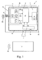
- Fig. 1 shows a schematic block circuit diagram of an RFID system comprising a data carrier according to the invention.
- Fig. 2 shows a schematic circuit diagram of a strain evaluating circuit to be used in a data carrier according to the invention.
- Fig. 3 shows a schematic circuit diagram of an alternative strain evaluating circuit to be used in a data carrier according to the invention.
- Fig. 4 shows a side view of the arrangement of strain sensors on opposite surfaces of a substrate.
- Fig. 5 shows a schematic block circuit diagram of an alternative configuration of strain gauge means.
- Fig. 1 shows a schematic block circuit diagram of an RFID (Radio Frequency Identification) system comprising an RFID data reader/writer 1 and a data carrier 2 configured as an RFID tag.
- the RFID data reader/writer 1 may be of conventional design, so it needs not to be explained in more detail. It is sufficient to mention that the RFID data reader/writer 1 communicates with the data carrier 2 in a contactless manner via RF data transmission means by modulated electromagnetic signals SS, provided the data carrier 2 is within a transmission and receiving range of the RFID data reader/writer 1.
- the electromagnetic signals SS spread from the RFID data reader/writer 1 may be used for both transmitting data to the data carrier 2 and energizing the data carrier 2 if it is configured as a passive tag.
- the data carrier 2 responds to the RFID data reader/writer 1 by modulating the received electromagnetic signals SS.
- a data exchange between the RFID data reader/writer 1 and the data carrier 2 may be accomplished by standard data transmission protocols and standard modulation methods.
- the electromagnetic signals SS sent from the RFID data reader/writer 1 to the data carrier 2 are configured as a pulse-width modulated signal.
- the logic response signals RS from the data carrier 2 to the RFID data reader/writer 1 are e.g. load-modulated signals, i.e. a carrier signal or sub-carrier signal contained in the electromagnetic signal SS is modulated by switching a load impedance connected to the antenna of the data carrier 2, so that varying energy is drawn from the carrier signal or sub-carrier signal. Switching the load impedances in the data carrier 2 causes a change of the impedance of the antenna of the RFID data reader/writer 1 and hence a varying amplitude of the voltage at the antenna of the RFID data reader/writer 1.
- the exemplary embodiment of the data carrier 2 according to the invention which is configured as a passive RFID tag, comprises RF data transmission means 10 in form of an antenna, an analogue radio frequency interface 11 that is connected to the RF data transmission means 10, a digital control unit 12 that is connected to the analogue radio frequency interface 11, and a memory 13 that is connected to the digital control unit 12.
- the analogue radio frequency interface 11, the digital control unit 12 and the memory 13 together constitute a data circuit 4 that is arranged on a substrate 3.
- the memory 13 is preferably embodied as a non-volatile memory, such as e.g.
- Memory 13 may also contain a program code for operating the digital control unit 12 and a unique identification number.
- RF data transmission means 10 receive the electromagnetic signals SS from the RFID data reader/writer 1 and pass them to the analogue radio frequency interface 11.
- the analogue radio frequency interface 11 comprises a rectifier REG and a voltage regulator VREG with an integrated energy storage element (e.g. a capacitor) to derive, from the received electromagnetic signals SS, a necessary operating voltage VDD for the digital control unit 12 and the memory 13. Furthermore, the analogue radio frequency interface 11 comprises a demodulator DEMOD to extract data DIN from the electromagnetic signals SS and pass them to the digital control unit 12. The digital control unit 12 processes the received data DIN and may respond to the RFID data reader/writer 1 by creating output data DOUT and passing them to the analogue radio frequency interface 11. Furthermore, the analogue radio frequency interface I comprises a modulator MOD which is able to modulate the output data DOUT and transmit the modulated signals as response signals RS via the RF data transmission means 10.
- an integrated energy storage element e.g. a capacitor
- the data carrier 2 further comprises at least one strain gauge means 7 being adapted to measure strains exerted on the substrate 3, and hence indirectly measure strains exerted on the data circuit 4, and to transmit a deactivating signal DE to the data circuit 4, strictly speaking, to the digital control unit 12 of the data circuit 4, if the measured strains exceed a defined deactivating strain threshold.
- the data circuit 4 is adapted to interrupt data exchange with the RFID data reader/writer 1 via the RF data transmission means 10, if it receives the deactivating signal DE.
- the strain gauge means 7 comprises a strain sensor 6 arranged on the substrate 3 and a strain evaluating circuit 5 having a measuring input 5a that is connected to the strain sensor 6.
- the strain sensor 6 delivers a physical quantity that corresponds to the strains exerted on the substrate 3, and the strain evaluating circuit 5 is adapted to compare the physical quantity delivered by the strain sensor 6 with a threshold value of the physical quantity that corresponds to a deactivating strain threshold and to generate the deactivating signal DE if the physical quantity of the strain sensor 6 exceeds the threshold value of the physical quantity.
- the strain sensor 6 is configured as an electric resistor having a resistance value that varies with the strain exerted on the resistor.
- the electric resistor is configured as a poly resistor.
- the strain sensor 6 is preferably arranged in a peripheral region of the substrate 3, so that it encompasses the data circuit 4, the electric resistor being applied in a thin meandering configuration.
- the strain sensor 6 configured as a resistor comprises four sections 6a, 6b, 6c, 6d, each located close to one of the four edges of the substrate 3, and the cross-sectional area and/or the meandering shape of the sections of the electric resistor possibly differing from each other in order to compensate anisotropic stiffness of the substrate 3. Examples of the strain evaluating circuit 5 will be given below.
- Interruption of data exchange between the RFID data reader/writer 1 and the data carrier 2 in the event of the occurrence of the deactivating signal DE can be handled in different ways.
- the digital control unit 12 of the data circuit 4 interrupts a data exchange with the RFID data reader/writer 1 only temporarily when the deactivating signal DE occurs.
- the deactivating signal DE disappears, because the strain exerted on the data carrier 2 has been relieved, the digital control unit 12 resumes the communication with the RFID data reader/writer 1.
- interruption of data exchange between the data carrier 2 and the RFID data reader/writer 1 as used herein means that the digital control unit 12 does not send data via the RF data transmission means 10, even if requested by the RFID data reader/writer 1, and disregards any data received from the RFID data reader/writer 1. Due to this behavior, on the one hand, the risk is significantly reduced that erroneous data - which have been corrupted in the data carrier 2 due to the exerted strains - will be used for further processing. On the other hand, when the deactivating signal DE disappears, data exchanged between the RFID data reader/writer 1 and the data carrier 2 is regarded as reliable and hence can be used for further processing.
- a strain occurrence flag SO is provided within the non-volatile memory 13. This strain occurrence flag SO is set by the digital control unit 12 on each occurrence of the deactivating signal, but will not be reset. A status of the strain occurrence flag SO can be read out from the non-volatile memory 13 by an external reading device, like the RFID data reader/writer 1.
- Permanent interruption of data exchange between the data carrier 2 and the RFID data reader/writer 1 can, for example, be chosen for another reason:
- a plurality of data circuits 4 are formed on a wafer.
- the data circuits 4 undergo a lot of functional tests during which they are still arranged on the wafer. After the functional tests, the wafers are cut in order to separate the data circuits 4.
- the data circuits 4 are usually fixed to a carrier, like a plastic or paper card or textiles, and are bonded to an antenna. These finishing manufacturing steps are the most critical ones, since the data circuits 4 are exposed to mechanical strains as well as to thermal and sometimes chemical stress.
- After the data carrier product has been finished usually merely a short final functional test is carried out. However, due to time pressure in the production plants the final functional test cannot include full functional test procedures.
- a data carrier product is released although it contains some defects that are the result of strains exerted on the data carrier 4 during the final manufacturing steps, e.g. caused by sawing misalignment, die crack, metal peel off, etc.
- a defect may be, for instance, that only a part of the non-volatile memory 13 can be used, because one or more memory cells or lines of the data bus have been broken.
- excessive strains which have changed parameters of the data carrier product permanently (which changed parameters are measured by the strain gauge means 7), cause the strain gauge means 7 to generate the deactivating signal DE which results in a permanent deactivation of the data carrier 2.
- the strain gauge means 7 comprise a strain sensor which is incorporated as an electrical resistor which changes its resistance in dependence on exerted strains
- the resistor may have been broken by excessive strains (resistance becomes infinite), or may have been permanently stretched by bending, twisting etc. (permanent increase of the resistance).
- the strain gauge means 7 can also be adapted to transmit a damage signal DA to the digital control unit 12 of the data circuit 4 if the measured strains exceed a defined damaging strain threshold, the data circuit 4 being adapted to permanently interrupt the data exchange with an external RFID data reader/writer 1 via the RF data transmission means 10 if the damaging signal DA is received.
- both the deactivating signal DE and the damage signal DA are used to discriminate between strains on the data carrier 4 that exceed a given deactivating strain threshold (but are regarded not to damage the data carrier 2) and strains that exceed a higher damaging strain threshold, so that permanent damage of the data carrier 2 has to be feared.
- a temporary interruption of data exchange is regarded as a sufficient measure of precaution in order to avoid possible transmission of corrupted data.
- the data circuit 4 is adapted to permanently interrupt the data exchange with the RFID data reader/writer 1.
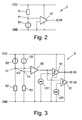
- Fig. 2 shows a schematic circuit diagram of a strain evaluating circuit 5 to be used in the data carriers 2 according to the present invention.
- This strain evaluating circuit 5 is configured as a single-bridge circuit, wherein a strain sensor in form of a strain-dependent resistor R1 and a constant current source IS1 are connected in series between the supply voltage VDD and ground potential GND, so that they form a voltage divider.
- a voltage dividing point P1 between the resistor R1 and the constant current source IS1 is connected to an input of an amplifier A1.
- An output signal of the amplifier A1 constitutes the deactivating signal DE. It should be observed that this basic circuit can be varied in various ways. For instance, the amplifier A1 could be replaced by an inverter.
- a comparator can be provided behind the amplifier A 1 having one input connected to the output of the amplifier A1 and having a second input connected to a reference voltage that represents a deactivating strain threshold.
- the output of the comparator constitutes the deactivating signal DE.
- Fig. 3 shows a schematic circuit diagram of another strain evaluating circuit 5' to be used in data carriers 2 according to the present invention.
- This alternative strain evaluating circuit 5' is configured as a modified Wheatstone bridge.
- a first strain sensor in form of a first strain-dependent resistor R2 and a first constant current source IS2 are connected in series between a supply voltage VDD and ground potential GND, so that they form a voltage divider with a first voltage dividing point P2 between the first resistor R2 and the first constant current source IS2.
- the first resistor R2 and the first constant current source IS2 connected in series constitute a first arm of the modified Wheatstone bridge.
- a second strain sensor in form of a second strain-dependent resistor R3 and a second constant current source IS3 are connected in series between the supply voltage VDD and ground potential GND, so that they form a voltage divider with a second voltage dividing point P3 between the second resistor R3 and the second constant current source IS3.
- the second resistor R3 and the second constant current source IS3 connected in series constitute a second arm of the modified Wheatstone bridge.
- the currents delivered by the first and second constant current sources IS2, IS3 and the resistances of the strain-dependent resistors R2, R3 are set so that the voltage difference ⁇ U appearing across the voltage dividing points P2, P3 is substantially zero when no strain is exerted on the resistors R2, R3, but deviates from zero when strains are exerted on the resistors R2, R3 due to different changes of the resistances of the respective resistors R2, R3.
- the voltage difference ⁇ U is fed to the input of an amplifier A2.
- the output signal of the amplifier A2 is fed to an input of a first comparator K1 having a second input connected to a first reference voltage UR1 that is representative of the deactivating strain threshold.
- a first comparator K1 having a second input connected to a first reference voltage UR1 that is representative of the deactivating strain threshold.
- the first comparator K1 generates the deactivating signal DE.
- the output signal of the amplifier A2 is also fed to an input of a second comparator K2 having a second input connected to a second reference voltage UR2 that is representative of a damaging strain threshold.
- the second comparator K2 When the output signal of the amplifier A2 exceeds the second reference voltage UR2, the second comparator K2 generates the damage signal DA.
- Both the deactivating signal DE and the damage signal DA are supplied to the digital control unit 12 (shown in Fig. 1 ).
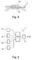
- the first strain-dependent resistor R2 is arranged on an upper surface of the substrate 3 and the second strain-dependent resistor R3 is arranged on a lower surface of the substrate 3, as shown in the side view of Fig. 4 .
- the first and second resistors R2, R3 are arranged in alignment with each other on opposite surfaces of the substrate 3.
- first strain-dependent resistor R2 has been arranged on an upper surface of the substrate 3 and only one second strain-dependent resistor R3 has been arranged on a lower surface of the substrate 3, according to the invention also a plurality of strain-dependent resistors may be arranged on the upper surface and a plurality of strain-dependent resistors may be arranged on the lower surface of the substrate in alignment with the resistors on the upper surface.
- the resistors need not be placed on the upper and lower surfaces of the substrate, but may also be embedded in, respectively, upper and lower layers of the substrate, like in a first or second poly-silicon layer, an active layer, an n-well layer, a p-well layer, or the like.
- Fig. 5 shows a schematic block circuit diagram of an alternative configuration of strain gauge means 7' to be used in the present invention.
- four separate strain sensors 6e, 6f, 6g, 6h are provided, whose output signals are fed to the inputs of a multiplexer MUX.
- An output of the multiplexer MUX is fed to the input of the strain evaluating circuit 5. If the strains exerted on the strain sensors 6e, 6f, 6g, 6h exceed a deactivating strain threshold in one ore more of the strain sensors 6e, 6f, 6g, 6h, the strain evaluating circuit 5 generates the deactivating signal DE.
Landscapes
- Engineering & Computer Science (AREA)
- Computer Hardware Design (AREA)
- Microelectronics & Electronic Packaging (AREA)
- General Physics & Mathematics (AREA)
- Theoretical Computer Science (AREA)
- Physics & Mathematics (AREA)
- Computer Security & Cryptography (AREA)
- General Engineering & Computer Science (AREA)
- Computer Networks & Wireless Communication (AREA)
- Artificial Intelligence (AREA)
- Computer Vision & Pattern Recognition (AREA)
- Measurement Of Length, Angles, Or The Like Using Electric Or Magnetic Means (AREA)
- Near-Field Transmission Systems (AREA)
- Arrangements For Transmission Of Measured Signals (AREA)
- Automatic Analysis And Handling Materials Therefor (AREA)
- Investigating Or Analysing Biological Materials (AREA)
Claims (17)
- Ein Datenträger (2), umfassend: eine Datenschaltung (4), die auf einem Substrat (3) angeordnet ist, und Datenübertragungsmittel (10), die mit der Datenschaltung (4) verbunden sind, wobei der Datenträger (2) mindestens ein Dehnungsmessmittel (7) umfasst, das so angepasst ist, dass es auf das Substrat (3) ausgeübte Dehnungen misst, dadurch gekennzeichnet, dass das Dehnungsmessmittel (7) so angeordnet ist, dass es ein Deaktivierungssignal (DE) an die Datenschaltung (4) überträgt, wenn die gemessenen Dehnungen einen definierten Deaktivierungsdehnungsschwellenwert überschreiten, wobei die Datenschaltung (4) so angepasst ist, dass sie einen Datenaustausch mit einem externen Datenleser/-schreiber (1) über die Datenübertragungsmittel (10) unterbricht, wenn die Datenschaltung (4) das Deaktivierungssignal (DE) empfängt.
- Der Datenträger nach Anspruch 1, wobei die Dehnungsmessmittel (7) umfassen: mindestens einen Dehnungssensor (6; 6e, 6f, 6g, 6h), der auf dem oder im Substrat (3) angeordnet ist, und eine Dehnungsauswertungsschaltung (5), die einen mit dem Dehnungssensor (6; 6e, 6f, 6g, 6h) verbundenen Messeingang aufweist, wobei der Dehnungssensor (6; 6e, 6f, 6g, 6h) eine physikalische Größe liefert, die den auf das Substrat (3) ausgeübten Dehnungen entspricht, und die Dehnungsauswertungsschaltung (5) so angepasst ist, dass sie die durch den Dehnungssensor (6; 6e, 6f, 6g, 6h) gelieferte physikalische Größe mit einem Schwellenwert der physikalischen Größe vergleicht, der einem Deaktivierungsdehnungsschwellenwert entspricht, und das Deaktivierungssignal (DE) erzeugt, wenn die physikalische Größe des Dehnungssensors (6; 6e, 6f, 6g, 6h) den Schwellenwert der physikalischen Größe überschreitet.
- Der Datenträger nach Anspruch 2, wobei der mindestens eine Dehnungssensor (6; 6e, 6f, 6g, 6h) mindestens einen elektrischen Widerstand (R1, R2, R3) umfasst, der einen Widerstandswert aufweist, der mit der auf den Widerstand (R1, R2, R3) ausgeübten Dehnung variiert.
- Der Datenträger nach Anspruch 3, wobei der elektrische Widerstand (R1, R2, R3) als Mehrfachwiderstand konfiguriert ist.
- Der Datenträger nach Anspruch 3 oder 4, wobei der elektrische Widerstand (R1, R2, R3) auf dem oder im Substrat (3) in einer Mäanderkonfiguration angeordnet ist.
- Der Datenträger nach Anspruch 2, wobei der mindestens eine Dehnungssensor (6, 6a, 6b, 6c, 6d) in einem peripheren Bereich des Substrats (3) angeordnet ist.
- Der Datenträger nach Anspruch 2 oder 6, wobei der mindestens eine Dehnungssensor (6) die Datenschaltung (4) zumindest teilweise umschließt.
- Der Datenträger nach Anspruch 3 oder 5, wobei die Querschnittsfläche und/oder die Mäanderform des elektrischen Widerstands (R1, R2, R3) in verschiedenen Abschnitten des elektrischen Widerstands verschieden ist.
- Der Datenträger nach Anspruch 2, wobei mindestens ein erster Dehnungssensor auf einer oberen Fläche des Substrats (3) angeordnet oder in eine obere Schicht desselben eingebettet ist und mindestens ein zweiter Dehnungssensor auf einer unteren Fläche des Substrats (3) angeordnet oder in eine untere Schicht desselben eingebettet ist, wobei die ersten und zweiten Dehnungssensoren vorzugsweise miteinander ausgerichtet auf gegenüberliegenden Flächen oder Schichten angeordnet sind und eine Differenz zwischen Ausgangssignalen der ersten und zweiten Dehnungssensoren verwendet wird, um die auf das Substrat (3) ausgeübte Dehnung auszuwerten.
- Der Datenträger nach Anspruch 2, wobei eine Mehrzahl von Dehnungssensoren (6e, 6f, 6g, 6h) vorgesehen ist, wobei die Ausgangssignale der Mehrzahl von Dehnungssensoren (6e, 6f, 6g, 6h) unabhängig ausgewertet werden und optional verschiedene Deaktivierungsdehnungsschwellenwerte fiir die Dehnungssensoren (6e, 6f, 6g, 6h) definiert sind.
- Der Datenträger nach Anspruch 3, wobei der elektrische Widerstand (R1; R2, R3) in eine Brückenschaltung geschaltet ist, wobei die Brückenschaltung so angepasst ist, dass sie den Widerstand des elektrischen Widerstands (R1; R2, R3) misst.
- Der Datenträger nach Anspruch 9, wobei die ersten und die zweiten Dehnungssensoren als dehnungsabhängige Widerstände (R2, R3) konfiguriert sind, die in eine Brückenschaltung geschaltet sind, wobei die Brückenschaltung so angepasst ist, dass sie die Differenz zwischen den Widerstandswerten der zwei dehnungsabhängigen Widerstände (R2, R3) misst.
- Der Datenträger nach Anspruch 1, wobei die Unterbrechung des Datenaustauschs über die Datenübertragungsmittel (10) aufrechterhalten wird, solange das Deaktivierungssignal (DE) auftritt.
- Der Datenträger nach Anspruch 1, wobei ein zeitweiliges Auftreten des Deaktivierungssignals (DE) dauerhaft in der Datenschaltung (4) gespeichert wird.
- Der Datenträger nach Anspruch 1, wobei beim zeitweiligen Auftreten des Deaktivierungssignals (DE) der Datenaustausch zwischen dem Datenträger (2) und dem externen Datenleser/-schreiber (1) dauerhaft unterbrochen wird.
- Der Datenträger nach Anspruch 1, wobei die Dehnungsmessmittel (7) so angepasst sind, dass sie ein Beschädigungssignal (DA) an die Datenschaltung (4) übertragen, wenn die gemessenen Dehnungen einen Schädigungsdehnungsschwellenwert überschreiten, wobei die Datenschaltung (4) so angepasst ist, dass sie den Datenaustausch mit dem externen Leser/Schreiber (1) über die Datenübertragungsmittel (10) dauerhaft unterbricht, wenn das Beschädigungssignal (DA) durch die Datenschaltung (4) empfangen wird.
- Der Datenträger nach Anspruch 2, wobei temperaturabhängige Änderungen des Ausgangssignals des Dehnungssensors (6) überwacht und in der Datenschaltung (4) registriert werden.
Priority Applications (1)
| Application Number | Priority Date | Filing Date | Title |
|---|---|---|---|
| EP07735234A EP2005369B1 (de) | 2006-03-30 | 2007-03-23 | Datenträger mit dehnungsmessung |
Applications Claiming Priority (3)
| Application Number | Priority Date | Filing Date | Title |
|---|---|---|---|
| EP06111969 | 2006-03-30 | ||
| EP07735234A EP2005369B1 (de) | 2006-03-30 | 2007-03-23 | Datenträger mit dehnungsmessung |
| PCT/IB2007/051022 WO2007113722A1 (en) | 2006-03-30 | 2007-03-23 | Data carrier comprising strain gauge means |
Publications (2)
| Publication Number | Publication Date |
|---|---|
| EP2005369A1 EP2005369A1 (de) | 2008-12-24 |
| EP2005369B1 true EP2005369B1 (de) | 2009-08-05 |
Family
ID=38326986
Family Applications (1)
| Application Number | Title | Priority Date | Filing Date |
|---|---|---|---|
| EP07735234A Active EP2005369B1 (de) | 2006-03-30 | 2007-03-23 | Datenträger mit dehnungsmessung |
Country Status (7)
| Country | Link |
|---|---|
| US (1) | US7884722B2 (de) |
| EP (1) | EP2005369B1 (de) |
| JP (1) | JP2009531769A (de) |
| CN (1) | CN101416205B (de) |
| AT (1) | ATE438901T1 (de) |
| DE (1) | DE602007001883D1 (de) |
| WO (1) | WO2007113722A1 (de) |
Families Citing this family (22)
| Publication number | Priority date | Publication date | Assignee | Title |
|---|---|---|---|---|
| MY151768A (en) * | 2007-02-28 | 2014-07-14 | Card Lab Aps | An electronic payment, information, or id card with a deformation sensing means |
| DE102009018187B4 (de) * | 2009-04-22 | 2022-10-06 | Trützschler Group SE | Vorrichtung zum Betrieb von Bedien- und Anzeigeeinheiten an Textilmaschinen und Anlagen, insbesondere im Bereich Spinnereimaschinen und -anlagen, z. B. Spinnereivorbereitungsmaschinen und -anlagen |
| JP2012039712A (ja) * | 2010-08-05 | 2012-02-23 | Toshiba Schneider Inverter Corp | インバータ装置、その周辺機器並びに梱包体 |
| DE102010052983A1 (de) * | 2010-11-30 | 2012-05-31 | Giesecke & Devrient Gmbh | Portabler Datenträger und Verfahren zu seiner Kalibrierung |
| DE102010054062A1 (de) * | 2010-12-10 | 2012-06-14 | Giesecke & Devrient Gmbh | Tragbarer Datenträger und Echtheitsprüfung durch Verformung |
| US8801711B2 (en) | 2011-06-16 | 2014-08-12 | Clifford T. Solomon | Skull clamp system with pressure limiting and alarm systems |
| DE102012209148A1 (de) * | 2012-05-31 | 2013-12-05 | Siemens Aktiengesellschaft | RFID-Tag und Verfahren zum Sichern eines RFID-Tags |
| US9000833B2 (en) * | 2013-03-06 | 2015-04-07 | Silicon Laboratories Inc. | Compensation of changes in MEMS capacitive transduction |
| US9489000B2 (en) | 2013-09-30 | 2016-11-08 | Silicon Laboratories Inc. | Use of a thermistor within a reference signal generator |
| US10254176B2 (en) | 2014-04-07 | 2019-04-09 | Silicon Laboratories Inc. | Strain-insensitive temperature sensor |
| US9377412B2 (en) * | 2014-04-16 | 2016-06-28 | Apple Inc. | Electronic device having components with stress visualization features |
| US9454684B2 (en) * | 2014-05-28 | 2016-09-27 | Taiwan Semiconductor Manufacturing Company Limited | Edge crack detection system |
| MA41187A (fr) | 2014-12-19 | 2021-04-07 | Cardlab Aps | Procédé et ensemble pour générer un champ magnétique et procédé de fabrication d'un ensemble |
| EP3035230A1 (de) | 2014-12-19 | 2016-06-22 | Cardlab ApS | Verfahren und Anordnung zum Erzeugen eines Magnetfeldes |
| WO2016136565A1 (ja) * | 2015-02-27 | 2016-09-01 | 株式会社村田製作所 | Rfモジュール及びrfシステム |
| EP3082071A1 (de) | 2015-04-17 | 2016-10-19 | Cardlab ApS | Vorrichtung und verfahren zur ausgabe eines magnetfelds |
| US9989927B1 (en) | 2016-11-30 | 2018-06-05 | Silicon Laboratories Inc. | Resistance-to-frequency converter |
| KR20200046282A (ko) * | 2018-10-24 | 2020-05-07 | 삼성전자주식회사 | 집적 회로 장치 및 고 대역폭 메모리 장치 |
| DE102019201954A1 (de) * | 2019-02-14 | 2020-08-20 | Fraunhofer-Gesellschaft zur Förderung der angewandten Forschung e.V. | Sensorelement zur Erfassung von Dehnungen bei der Bewegung eines Körperteils eines Lebewesens |
| FR3108408B1 (fr) * | 2020-03-18 | 2022-03-25 | Asygn | Circuit pour étiquette de radio-identification passive comprenant un capteur de contrainte et procédé pour fabriquer un circuit |
| CN113191475B (zh) * | 2021-05-21 | 2023-10-20 | 上海坤锐电子科技有限公司 | 无源返回传感器信息的电路、电子标签系统 |
| DE102022115164A1 (de) * | 2022-06-16 | 2023-12-21 | Olympus Winter & Ibe Gmbh | Chirurgisches Werkzeug und elektrochirurgisches Handinstrument sowie Verfahren zur Erkennung eines chirurgischen Werkzeugs |
Family Cites Families (8)
| Publication number | Priority date | Publication date | Assignee | Title |
|---|---|---|---|---|
| JPH02307792A (ja) | 1989-05-23 | 1990-12-20 | Canon Inc | Icカード |
| FR2649817B1 (fr) | 1989-07-13 | 1993-12-24 | Gemplus Card International | Carte a microcircuit protegee contre l'intrusion |
| DE19947180A1 (de) | 1999-10-01 | 2001-04-05 | Philips Corp Intellectual Pty | Chipkarte |
| GB0102882D0 (en) | 2001-02-06 | 2001-03-21 | Koninkl Philips Electronics Nv | Signalling system and a transport for use in the system |
| DE10154495C5 (de) | 2001-11-07 | 2018-01-11 | Infineon Technologies Ag | Konzept zur Kompensation der Einflüsse externer Störgrößen auf physikalische Funktionsparameter von integrierten Schaltungen |
| US7098794B2 (en) | 2004-04-30 | 2006-08-29 | Kimberly-Clark Worldwide, Inc. | Deactivating a data tag for user privacy or tamper-evident packaging |
| JP2005327104A (ja) * | 2004-05-14 | 2005-11-24 | Oki Electric Ind Co Ltd | 非接触データキャリア、質問器、非接触データキャリアシステム、非接触データキャリアのデータ取得方法、及び、非接触データキャリアのデータ取得用プログラム |
| US20070096882A1 (en) * | 2005-11-02 | 2007-05-03 | Symbol Technologies, Inc. | Sensor based selection of radio frequency identification tags |
-
2007
- 2007-03-23 EP EP07735234A patent/EP2005369B1/de active Active
- 2007-03-23 CN CN2007800124055A patent/CN101416205B/zh not_active Expired - Fee Related
- 2007-03-23 US US12/293,814 patent/US7884722B2/en active Active
- 2007-03-23 WO PCT/IB2007/051022 patent/WO2007113722A1/en not_active Ceased
- 2007-03-23 AT AT07735234T patent/ATE438901T1/de not_active IP Right Cessation
- 2007-03-23 JP JP2009502289A patent/JP2009531769A/ja not_active Withdrawn
- 2007-03-23 DE DE602007001883T patent/DE602007001883D1/de active Active
Also Published As
| Publication number | Publication date |
|---|---|
| DE602007001883D1 (de) | 2009-09-17 |
| US20100225483A1 (en) | 2010-09-09 |
| CN101416205B (zh) | 2011-07-27 |
| JP2009531769A (ja) | 2009-09-03 |
| US7884722B2 (en) | 2011-02-08 |
| ATE438901T1 (de) | 2009-08-15 |
| EP2005369A1 (de) | 2008-12-24 |
| CN101416205A (zh) | 2009-04-22 |
| WO2007113722A1 (en) | 2007-10-11 |
Similar Documents
| Publication | Publication Date | Title |
|---|---|---|
| EP2005369B1 (de) | Datenträger mit dehnungsmessung | |
| CN107437106B (zh) | 篡改检测装置 | |
| US8933781B2 (en) | Fingerprint reader and a method of operating it | |
| CN103493111B (zh) | 用于探测rfid移除的方法、系统和装置 | |
| US7205899B2 (en) | Flexible transponder label which is readable on conductive surfaces | |
| CN101443262B (zh) | 一种用于气体和液体系统的耦合装置和包括该装置的用于车辆的无线信号传输系统 | |
| US20040061655A1 (en) | Environmentally sensitive multi-frequency antenna | |
| US20120176223A1 (en) | Wireless ic device and method of detecting environmental state using the device | |
| US6420883B1 (en) | Semiconductor integrated circuit device and IC card | |
| EP3350751B1 (de) | Rfid-etikett mit manipulationssicherer anordnung | |
| CN102132293A (zh) | 混合传感器/通信设备和方法 | |
| TWM330556U (en) | Load board with radio frequency identification (RFID) tag function | |
| KR100366932B1 (ko) | 반도체 장치 및 그의 제조 방법 | |
| EP2793018A1 (de) | Auf Wärmeleitfähigkeit basierender Gassensor | |
| JPH02307792A (ja) | Icカード | |
| JP2000132654A (ja) | 非接触データキャリアパッケージ | |
| EP4338095B1 (de) | Rfid-sensoranordnung und verfahren zu ihrer herstellung | |
| KR101021741B1 (ko) | 시온 기능을 갖는 rf 태그 장치 | |
| AU2015200615B2 (en) | A fingerprint reader and a method of operating it | |
| JP2006058014A (ja) | 温度変化検出機能付き非接触型のデータキャリア | |
| JP2018013943A (ja) | モニタリングタグ | |
| Lee | RFID Tag and COB Development Guide with Microchip’s RFID Devices | |
| HK1156130B (en) | A fingerprint reader and a method of operating it | |
| JP2010244257A (ja) | データキャリア及びリーダ/ライタ装置 |
Legal Events
| Date | Code | Title | Description |
|---|---|---|---|
| PUAI | Public reference made under article 153(3) epc to a published international application that has entered the european phase |
Free format text: ORIGINAL CODE: 0009012 |
|
| 17P | Request for examination filed |
Effective date: 20081030 |
|
| AK | Designated contracting states |
Kind code of ref document: A1 Designated state(s): AT BE BG CH CY CZ DE DK EE ES FI FR GB GR HU IE IS IT LI LT LU LV MC MT NL PL PT RO SE SI SK TR |
|
| AX | Request for extension of the european patent |
Extension state: AL BA HR MK RS |
|
| GRAP | Despatch of communication of intention to grant a patent |
Free format text: ORIGINAL CODE: EPIDOSNIGR1 |
|
| GRAS | Grant fee paid |
Free format text: ORIGINAL CODE: EPIDOSNIGR3 |
|
| GRAA | (expected) grant |
Free format text: ORIGINAL CODE: 0009210 |
|
| AK | Designated contracting states |
Kind code of ref document: B1 Designated state(s): AT BE BG CH CY CZ DE DK EE ES FI FR GB GR HU IE IS IT LI LT LU LV MC MT NL PL PT RO SE SI SK TR |
|
| AX | Request for extension of the european patent |
Extension state: AL BA HR MK RS |
|
| REG | Reference to a national code |
Ref country code: GB Ref legal event code: FG4D |
|
| REG | Reference to a national code |
Ref country code: CH Ref legal event code: EP |
|
| REG | Reference to a national code |
Ref country code: IE Ref legal event code: FG4D |
|
| REF | Corresponds to: |
Ref document number: 602007001883 Country of ref document: DE Date of ref document: 20090917 Kind code of ref document: P |
|
| LTIE | Lt: invalidation of european patent or patent extension |
Effective date: 20090805 |
|
| PG25 | Lapsed in a contracting state [announced via postgrant information from national office to epo] |
Ref country code: AT Free format text: LAPSE BECAUSE OF FAILURE TO SUBMIT A TRANSLATION OF THE DESCRIPTION OR TO PAY THE FEE WITHIN THE PRESCRIBED TIME-LIMIT Effective date: 20090805 Ref country code: ES Free format text: LAPSE BECAUSE OF FAILURE TO SUBMIT A TRANSLATION OF THE DESCRIPTION OR TO PAY THE FEE WITHIN THE PRESCRIBED TIME-LIMIT Effective date: 20091116 Ref country code: FI Free format text: LAPSE BECAUSE OF FAILURE TO SUBMIT A TRANSLATION OF THE DESCRIPTION OR TO PAY THE FEE WITHIN THE PRESCRIBED TIME-LIMIT Effective date: 20090805 Ref country code: IS Free format text: LAPSE BECAUSE OF FAILURE TO SUBMIT A TRANSLATION OF THE DESCRIPTION OR TO PAY THE FEE WITHIN THE PRESCRIBED TIME-LIMIT Effective date: 20091205 Ref country code: LT Free format text: LAPSE BECAUSE OF FAILURE TO SUBMIT A TRANSLATION OF THE DESCRIPTION OR TO PAY THE FEE WITHIN THE PRESCRIBED TIME-LIMIT Effective date: 20090805 Ref country code: SE Free format text: LAPSE BECAUSE OF FAILURE TO SUBMIT A TRANSLATION OF THE DESCRIPTION OR TO PAY THE FEE WITHIN THE PRESCRIBED TIME-LIMIT Effective date: 20090805 |
|
| NLV1 | Nl: lapsed or annulled due to failure to fulfill the requirements of art. 29p and 29m of the patents act | ||
| PG25 | Lapsed in a contracting state [announced via postgrant information from national office to epo] |
Ref country code: NL Free format text: LAPSE BECAUSE OF FAILURE TO SUBMIT A TRANSLATION OF THE DESCRIPTION OR TO PAY THE FEE WITHIN THE PRESCRIBED TIME-LIMIT Effective date: 20090805 Ref country code: LV Free format text: LAPSE BECAUSE OF FAILURE TO SUBMIT A TRANSLATION OF THE DESCRIPTION OR TO PAY THE FEE WITHIN THE PRESCRIBED TIME-LIMIT Effective date: 20090805 Ref country code: PL Free format text: LAPSE BECAUSE OF FAILURE TO SUBMIT A TRANSLATION OF THE DESCRIPTION OR TO PAY THE FEE WITHIN THE PRESCRIBED TIME-LIMIT Effective date: 20090805 Ref country code: SI Free format text: LAPSE BECAUSE OF FAILURE TO SUBMIT A TRANSLATION OF THE DESCRIPTION OR TO PAY THE FEE WITHIN THE PRESCRIBED TIME-LIMIT Effective date: 20090805 |
|
| PG25 | Lapsed in a contracting state [announced via postgrant information from national office to epo] |
Ref country code: PT Free format text: LAPSE BECAUSE OF FAILURE TO SUBMIT A TRANSLATION OF THE DESCRIPTION OR TO PAY THE FEE WITHIN THE PRESCRIBED TIME-LIMIT Effective date: 20091205 Ref country code: BG Free format text: LAPSE BECAUSE OF FAILURE TO SUBMIT A TRANSLATION OF THE DESCRIPTION OR TO PAY THE FEE WITHIN THE PRESCRIBED TIME-LIMIT Effective date: 20091105 |
|
| PG25 | Lapsed in a contracting state [announced via postgrant information from national office to epo] |
Ref country code: EE Free format text: LAPSE BECAUSE OF FAILURE TO SUBMIT A TRANSLATION OF THE DESCRIPTION OR TO PAY THE FEE WITHIN THE PRESCRIBED TIME-LIMIT Effective date: 20090805 Ref country code: RO Free format text: LAPSE BECAUSE OF FAILURE TO SUBMIT A TRANSLATION OF THE DESCRIPTION OR TO PAY THE FEE WITHIN THE PRESCRIBED TIME-LIMIT Effective date: 20090805 Ref country code: DK Free format text: LAPSE BECAUSE OF FAILURE TO SUBMIT A TRANSLATION OF THE DESCRIPTION OR TO PAY THE FEE WITHIN THE PRESCRIBED TIME-LIMIT Effective date: 20090805 Ref country code: CZ Free format text: LAPSE BECAUSE OF FAILURE TO SUBMIT A TRANSLATION OF THE DESCRIPTION OR TO PAY THE FEE WITHIN THE PRESCRIBED TIME-LIMIT Effective date: 20090805 |
|
| PG25 | Lapsed in a contracting state [announced via postgrant information from national office to epo] |
Ref country code: SK Free format text: LAPSE BECAUSE OF FAILURE TO SUBMIT A TRANSLATION OF THE DESCRIPTION OR TO PAY THE FEE WITHIN THE PRESCRIBED TIME-LIMIT Effective date: 20090805 |
|
| PLBE | No opposition filed within time limit |
Free format text: ORIGINAL CODE: 0009261 |
|
| STAA | Information on the status of an ep patent application or granted ep patent |
Free format text: STATUS: NO OPPOSITION FILED WITHIN TIME LIMIT |
|
| PG25 | Lapsed in a contracting state [announced via postgrant information from national office to epo] |
Ref country code: BE Free format text: LAPSE BECAUSE OF FAILURE TO SUBMIT A TRANSLATION OF THE DESCRIPTION OR TO PAY THE FEE WITHIN THE PRESCRIBED TIME-LIMIT Effective date: 20090805 |
|
| 26N | No opposition filed |
Effective date: 20100507 |
|
| PG25 | Lapsed in a contracting state [announced via postgrant information from national office to epo] |
Ref country code: MC Free format text: LAPSE BECAUSE OF NON-PAYMENT OF DUE FEES Effective date: 20100331 Ref country code: GR Free format text: LAPSE BECAUSE OF FAILURE TO SUBMIT A TRANSLATION OF THE DESCRIPTION OR TO PAY THE FEE WITHIN THE PRESCRIBED TIME-LIMIT Effective date: 20091106 |
|
| PG25 | Lapsed in a contracting state [announced via postgrant information from national office to epo] |
Ref country code: IE Free format text: LAPSE BECAUSE OF NON-PAYMENT OF DUE FEES Effective date: 20100323 |
|
| PG25 | Lapsed in a contracting state [announced via postgrant information from national office to epo] |
Ref country code: IT Free format text: LAPSE BECAUSE OF FAILURE TO SUBMIT A TRANSLATION OF THE DESCRIPTION OR TO PAY THE FEE WITHIN THE PRESCRIBED TIME-LIMIT Effective date: 20090805 |
|
| PG25 | Lapsed in a contracting state [announced via postgrant information from national office to epo] |
Ref country code: MT Free format text: LAPSE BECAUSE OF FAILURE TO SUBMIT A TRANSLATION OF THE DESCRIPTION OR TO PAY THE FEE WITHIN THE PRESCRIBED TIME-LIMIT Effective date: 20090805 |
|
| REG | Reference to a national code |
Ref country code: CH Ref legal event code: PL |
|
| PG25 | Lapsed in a contracting state [announced via postgrant information from national office to epo] |
Ref country code: CH Free format text: LAPSE BECAUSE OF NON-PAYMENT OF DUE FEES Effective date: 20110331 Ref country code: LI Free format text: LAPSE BECAUSE OF NON-PAYMENT OF DUE FEES Effective date: 20110331 |
|
| PG25 | Lapsed in a contracting state [announced via postgrant information from national office to epo] |
Ref country code: CY Free format text: LAPSE BECAUSE OF FAILURE TO SUBMIT A TRANSLATION OF THE DESCRIPTION OR TO PAY THE FEE WITHIN THE PRESCRIBED TIME-LIMIT Effective date: 20090805 |
|
| PG25 | Lapsed in a contracting state [announced via postgrant information from national office to epo] |
Ref country code: LU Free format text: LAPSE BECAUSE OF NON-PAYMENT OF DUE FEES Effective date: 20100323 Ref country code: HU Free format text: LAPSE BECAUSE OF FAILURE TO SUBMIT A TRANSLATION OF THE DESCRIPTION OR TO PAY THE FEE WITHIN THE PRESCRIBED TIME-LIMIT Effective date: 20100206 |
|
| PG25 | Lapsed in a contracting state [announced via postgrant information from national office to epo] |
Ref country code: TR Free format text: LAPSE BECAUSE OF FAILURE TO SUBMIT A TRANSLATION OF THE DESCRIPTION OR TO PAY THE FEE WITHIN THE PRESCRIBED TIME-LIMIT Effective date: 20090805 |
|
| REG | Reference to a national code |
Ref country code: FR Ref legal event code: PLFP Year of fee payment: 9 |
|
| REG | Reference to a national code |
Ref country code: FR Ref legal event code: PLFP Year of fee payment: 10 |
|
| REG | Reference to a national code |
Ref country code: FR Ref legal event code: PLFP Year of fee payment: 11 |
|
| REG | Reference to a national code |
Ref country code: FR Ref legal event code: PLFP Year of fee payment: 12 |
|
| P01 | Opt-out of the competence of the unified patent court (upc) registered |
Effective date: 20230724 |
|
| PGFP | Annual fee paid to national office [announced via postgrant information from national office to epo] |
Ref country code: DE Payment date: 20240220 Year of fee payment: 18 Ref country code: GB Payment date: 20240220 Year of fee payment: 18 |
|
| PGFP | Annual fee paid to national office [announced via postgrant information from national office to epo] |
Ref country code: FR Payment date: 20240220 Year of fee payment: 18 |
|
| REG | Reference to a national code |
Ref country code: DE Ref legal event code: R119 Ref document number: 602007001883 Country of ref document: DE |
|
| GBPC | Gb: european patent ceased through non-payment of renewal fee |
Effective date: 20250323 |
|
| PG25 | Lapsed in a contracting state [announced via postgrant information from national office to epo] |
Ref country code: DE Free format text: LAPSE BECAUSE OF NON-PAYMENT OF DUE FEES Effective date: 20251001 |
|
| PG25 | Lapsed in a contracting state [announced via postgrant information from national office to epo] |
Ref country code: GB Free format text: LAPSE BECAUSE OF NON-PAYMENT OF DUE FEES Effective date: 20250323 |
|
| PG25 | Lapsed in a contracting state [announced via postgrant information from national office to epo] |
Ref country code: FR Free format text: LAPSE BECAUSE OF NON-PAYMENT OF DUE FEES Effective date: 20250331 |