EP2001129A2 - Signalverarbeitungsvorrichtung und Signalverarbeitungsverfahren - Google Patents
Signalverarbeitungsvorrichtung und Signalverarbeitungsverfahren Download PDFInfo
- Publication number
- EP2001129A2 EP2001129A2 EP08008707A EP08008707A EP2001129A2 EP 2001129 A2 EP2001129 A2 EP 2001129A2 EP 08008707 A EP08008707 A EP 08008707A EP 08008707 A EP08008707 A EP 08008707A EP 2001129 A2 EP2001129 A2 EP 2001129A2
- Authority
- EP
- European Patent Office
- Prior art keywords
- filter
- signal
- signal processing
- characteristic
- predetermined
- Prior art date
- Legal status (The legal status is an assumption and is not a legal conclusion. Google has not performed a legal analysis and makes no representation as to the accuracy of the status listed.)
- Granted
Links
- 238000012545 processing Methods 0.000 title claims abstract description 88
- 238000000034 method Methods 0.000 title claims abstract description 8
- 238000012937 correction Methods 0.000 claims abstract description 86
- 238000001514 detection method Methods 0.000 claims abstract description 56
- 230000005540 biological transmission Effects 0.000 claims abstract description 32
- 238000004590 computer program Methods 0.000 claims abstract description 7
- 238000003672 processing method Methods 0.000 claims abstract description 6
- 238000013016 damping Methods 0.000 claims abstract description 5
- 238000012546 transfer Methods 0.000 claims description 32
- 238000011144 upstream manufacturing Methods 0.000 claims description 8
- 230000004044 response Effects 0.000 claims description 6
- 230000003014 reinforcing effect Effects 0.000 abstract 1
- 230000015654 memory Effects 0.000 description 24
- 230000003321 amplification Effects 0.000 description 9
- 238000003199 nucleic acid amplification method Methods 0.000 description 9
- 230000006870 function Effects 0.000 description 7
- 238000010586 diagram Methods 0.000 description 5
- 238000005259 measurement Methods 0.000 description 3
- 230000001419 dependent effect Effects 0.000 description 2
- 238000011161 development Methods 0.000 description 2
- 230000018109 developmental process Effects 0.000 description 2
- 230000006978 adaptation Effects 0.000 description 1
- 238000006243 chemical reaction Methods 0.000 description 1
- 230000003111 delayed effect Effects 0.000 description 1
- 238000013461 design Methods 0.000 description 1
- 230000000694 effects Effects 0.000 description 1
Images

Classifications
-
- H—ELECTRICITY
- H03—ELECTRONIC CIRCUITRY
- H03G—CONTROL OF AMPLIFICATION
- H03G1/00—Details of arrangements for controlling amplification
-
- H—ELECTRICITY
- H03—ELECTRONIC CIRCUITRY
- H03G—CONTROL OF AMPLIFICATION
- H03G3/00—Gain control in amplifiers or frequency changers
- H03G3/20—Automatic control
- H03G3/30—Automatic control in amplifiers having semiconductor devices
- H03G3/3052—Automatic control in amplifiers having semiconductor devices in bandpass amplifiers (H.F. or I.F.) or in frequency-changers used in a (super)heterodyne receiver
Definitions
- the present invention relates to a signal processing apparatus and a signal processing method.
- a circuit for detecting the power of an input signal of a receiver system comprises a number of automatic gain control analog amplifiers, a fixed filter characteristic selective filter, an analog mixer and measuring means for measuring the power of an output signal for a predetermined frequency. Further, calculating means for detecting the power of the input signal, amplifying the number of analog amplifiers, and amplifying the analog selective filter for the predetermined frequency are provided by calibrating parameters of filter functions for different frequency ranges.
- the invention is based on the finding that the change in the transmission characteristic of the signal processing element - in particular a Filters - can be at least partially compensated by correcting a detection value obtained on the basis of the output signal of the signal processing element, which represents a characteristic output quantity, such as the power.
- Correcting the (i.a scalar) detection value processes a scalar quantity, not, for example, the entire output of the signal processing element.
- Each predetermined transfer characteristic may be pre-assigned predetermined correction values and e.g. be filed in a look-up table.
- the invention provides a signal processing device having a signal processing element with, for example, adjustable filter coefficients for an adjustable transfer characteristic, e.g. a predetermined transfer function or a predetermined impulse response or a predetermined attenuation characteristic or a predetermined gain.
- an adjustable transfer characteristic e.g. a predetermined transfer function or a predetermined impulse response or a predetermined attenuation characteristic or a predetermined gain.
- the signal processing device has an application device, which is connected downstream of the filter for amplifying or damping an output signal of the filter.
- the biasing means is adapted to partially compensate for an influence of the predetermined transmission characteristic of the filter on a characteristic magnitude of an input signal, wherein the compensation is associated with a residual error.
- the signal processing apparatus includes detecting means for detecting a characteristic magnitude of an output signal of the signal processing element, wherein the detecting means is adapted to output a detection value representing the characteristic magnitude of the output signal.
- the signal processing device has a correction device for applying the detection value with a predetermined correction value at least partial compensation of the residual error.
- the correction value is associated with the predetermined transfer characteristic.
- the signal processing device comprises a control device for setting the predetermined filter coefficients of the filter, the predetermined amplification or damping of the application device and the predetermined correction value of the correction device.
- the characteristic magnitude of the output signal represents a characteristic magnitude of an input signal of the signal processing element.
- the correction means is further adapted to apply the detection value to the predetermined correction value, e.g. by an addition or multiplication to at least partially compensate for the influence of the predetermined transfer characteristic on the characteristic size of the input signal of the signal processing element.
- the characteristic magnitude of the input or the output signal is the power or the energy or the amplitude or the phase.
- the detection device is designed to measure the characteristic size of the output signal.
- the detector performs an RSSI measurement to determine the power of the output signal.
- control means is arranged to select the predetermined transmission characteristic from a plurality of transmission characteristics, wherein each transmission characteristic of the plurality of transmission characteristics is assigned a correction value.
- the transmission characteristics which are determined for example by filter coefficients or coefficients of an impulse response, can be provided, for example, in the form of coefficients in a memory and retrieved therefrom.
- control device is designed to provide the correction device with the predetermined correction value, which may be stored, for example, in a look-up table.
- the signal processing device further comprises an application device, which is connected downstream of the signal processing element and receives its output signal.
- the biasing means is adapted to apply to the output signal, for example additively or multiplicatively, a predetermined bias value associated with the predetermined transmission characteristic or the predetermined correction value, e.g. at least reduce the influence of the change in the transfer characteristic of the signal processing element on the characteristic size of the output signal.
- control means is arranged to select the predetermined transmission characteristic from a plurality of transmission characteristics, each transmission characteristic of the plurality of transmission characteristics being associated with an application value.
- the loading values may e.g. be provided in a look-up table.
- control device is designed to provide the predetermined application value of the application device.
- the characteristic quantity of the output signal represents a characteristic quantity of an input signal of the signal processing element, eg the power.
- the application device is preferably designed to apply a predetermined application value to the output signal in order to at least partially compensate for the influence of the predetermined transfer characteristic on the characteristic size of the input signal.
- the correction device is further configured to influence the detection value by applying a remaining after the at least partial compensation influence of the predetermined transfer function the same with the predetermined correction value at least partially compensate. This two-stage concept ensures that the correction values for the correction of the detection value are low.
- the Beauftschungswert is preferably a power of two, for example 2 ⁇ N or 2 ⁇ (- N), where N, for example, is a natural number.
- the signal processing element is a filter, e.g. a bandpass filter, with adjustable filter coefficients.
- the controller preferably changes the filter coefficients of the filter to adjust the predetermined transfer characteristic by setting predetermined filter coefficients.
- the signal processing device comprises a further signal processing element with adjustable transmission characteristic, which is connected upstream of the signal processing element. Between the further signal processing element and the signal processing element, a further loading device can also be provided.
- the control device is designed to set a further predetermined transmission characteristic of the further signal processing element.
- the correction device is preferably designed to apply the detection value to a total correction value which represents an overlay of the predetermined correction value associated with the predetermined transfer characteristic and a further predetermined factor associated with the further predetermined transfer characteristic.
- the correction device can have one, two or more adders which add the correction values and the detection value.
- the invention provides a signal processing device with a detection device, an adjustable digital filter as a signal processing element, a digital multiplier as an application device and a correction device.
- the detection device is designed to detect a signal strength of a signal.
- one of the detection device can be output Detection value the signal strength of the signal.
- a signal strength can be represented, for example, by means of an RSSI value.
- the adjustable digital filter is connected upstream of the detection device in the signal path and influences the signal according to its transmission characteristic.
- Filter coefficients for adjusting the transfer characteristic of the filter are associated with a gain or attenuation of the signal by the filter.
- the gain or attenuation of the signal is predetermined by the filter coefficients.
- the digital multiplier is connected upstream of the detection device for amplification or attenuation of the signal.
- the multiplier is designed to only partially compensate for the gain or attenuation of the filter.
- the compensation is subject to a residual error.
- the signal is amplified by the multiplier, preferably by the factor 1 / (2 ⁇ N), where N can be a positive or negative integer.
- the residual error is determined by the difference between the gain or attenuation by the filter and the approximate gain corresponding to the factor 1 / (2 ⁇ N) of the multiplier.
- the correction device is designed to apply the detection value with a correction value that at least partially compensates for the residual error.
- the applying correction means is configured to add a logarithmic detection value having a logarithmic correction value.
- Another aspect of the invention is a use of a filter, a multiplier and a correction device for signal processing.
- the attenuation or amplification of the multiplier device and the correction value of the correction device are predetermined and assigned to the predetermined transmission characteristic of the filter.
- values for damping or Gain and the correction values stored in a table and assigned to the predetermined transmission characteristic, for example by pointers.
- the attenuation or amplification of the multiplier and the correction value of the correction device and the transmission characteristic of the filter can be controlled together by exactly one signal.
- the multiplier is designed to multiply the signal by a factor as a shift register or as a multiplexer or as a gate logic.
- the filter is designed as a bandpass filter, wherein by means of the filter coefficients a bandwidth is adjustable as a transmission characteristic of the bandpass filter.
- the invention provides a signal processing method comprising the step of processing a signal by a signal processing element having a transfer characteristic to obtain an output signal, the step of setting a predetermined transfer characteristic of the signal processing element, the step of detecting a characteristic magnitude of an output signal the signal processing element, the step of outputting a detection value representing the characteristic magnitude of the output signal and the step of biasing the detection value with a predetermined correction value associated with the predetermined transmission characteristic.
- the signal processing method comprises the step of biasing the output of the signal processing element with a predetermined bias value associated with the predetermined transmission characteristic or the predetermined correction value.
- the characteristic magnitude of the output signal represents a characteristic magnitude of an input signal of the output signal Signal processing element.
- the output signal is preferably applied with the predetermined bias value to at least partially compensate for the influence of the predetermined transfer characteristic on the characteristic amount of the input signal of the signal processing element.
- the detection value is preferably applied to the predetermined correction value in order to at least partially compensate for an influence of the predetermined transfer function remaining after the at least partial compensation on the detection value.
- the invention provides a computer program for carrying out the method according to the invention when the computer program runs on a computer.
- the invention provides a program-equipped data processing device which is designed to run the computer program in order to carry out the steps of the method according to the invention.
- Fig. 1 shows a block diagram of a signal processing device with a digital signal processing module 101 having at least one digital signal processing element.
- the signal processing apparatus has a digital controller 103 for setting a predetermined transfer characteristic of the signal processing element by, for example, exchanging the coefficients that determine the transfer characteristic.
- the A signal processing device comprises a digital detection means 105 for detecting a characteristic quantity of an output signal of the signal processing element 101 and a correction means 107 for applying a detection value provided by the detection means 105 to a predetermined correction value, the correction value being associated with the predetermined transmission characteristic.
- Fig. 2 shows a block diagram of a signal processing device with a first signal processing element 201, the output of which is coupled via a first application device 203 to an input of a second signal processing element 205.
- An output of the second signal processing element 205 is coupled to a detection device 209 via a second application device 207.
- An output of the detection device 209 is coupled to an input of an adder 211 of a correction device.
- the signal processing device further comprises a further (optional) adder 213, which is assigned to the first signal processing element 201, and a further adder 215, which is assigned to the second signal processing element 205.
- the optional adder 213 includes an optional input for receiving further correction values that may be associated with other signal processing elements (not shown).
- a further input of the optional adder 213 is connected to an output of a first memory element 217, wherein an output of the optional adder 213 is connected to an input of the further adder 215.
- Another input of the further adder 215 is connected to an output of a second memory element 219.
- An output of the further adder 215 is coupled to a further input of the correction device 211.
- the signal processing device further comprises a third memory element 221, which is coupled to a control input of the first biasing device 203, and a fourth memory element 223, which is coupled to a control input of the second biasing device 207. Furthermore, a first control connection 225 and a second control connection 227 are provided.
- the first Control terminal 225 is connected to a control input of the first signal processing element 201, via a delay element 202 to a control input of the first memory element 217 and to a control input of the third memory element 221.
- the second control terminal 227 is connected to a control input of the second signal processing element 205, via a delay element 204 to a control input of the second memory element 219 and to a control input of the fourth memory element 223.
- the first signal processing element 201 and the second signal processing element 205 are filters (BP1, BP2) with adjustable coefficients, which allows a flexible adaptation of the filter characteristic.
- the exchange of the coefficients of the respective filter can be initiated, for example, by control signals s BW1 , BW2 , which can be applied to the control terminals 225 and 227, respectively.
- the coefficients corresponding to the content of the respective control signal s BW1 , BW2 are set in the respective filter 201, 205.
- the filter 201 and / or the filter 205 may have a memory in which a plurality of coefficient sets are stored.
- the control signals s BW1 , BW2 can also be applied respectively to the memory elements 217, 219, 221 and 223, which in response thereto select the factors corresponding to the respective filter characteristic determined by the coefficients.
- the storage elements 221 and 223 select and supply the respective application values (n1, n2) to the respective application devices 203 and 207, respectively.
- the application devices 203 and 207 can be amplification or attenuation elements, for example, corresponding to the respective signal according to FIG. 2 ⁇ N), where N can be a positive or negative, preferably natural number.
- the application devices 203 and 207 are designed as multipliers.
- Each multiplier 203 or 207 can be designed as a multiplier.
- each multiplier 203 or 207 is preferably designed as a shift register, or multiplexer or gate logic.
- a design as a shift register or multiplexer or gate logic allows easy shifting of input bit values with respect to their significance. This is particularly easy to implement.
- the storage elements 221 and 223 select the above-mentioned powers of two as load values n, n1, n2, which may each be different.
- the memory elements 221 and 223 may select only the (positive and negative) integers N, which may each be different, and provide them to the respective apply means 203 and 207, respectively, for gain or attenuation.
- the control signals s BW1 , BW2 are further forwarded to the memory elements 217 and 219, for example, respectively delayed by the delay element 202 or 204 which, in response thereto, the corresponding correction values (Rest1, Rest2) as a function of one of the gain or attenuation filters remaining from filters 201 and 205, respectively, and applying devices 203 and 207, respectively, which may be different for the adders 213 and 215.
- the memory elements 217 and 219 provide the respective correction values to the respective adders 213 and 215, respectively.
- the adders 213 and 215 sum the correction values, and an overall correction value is superimposed on the detection value by means of the adder 211 as part of a correction device.
- the correction values can be, for example, logarithmic numbers based on 1d2.
- the respective correction values and the respective application values each form a predetermined factor pair which is assigned to the respective filter characteristic of the filter 201 or 205.
- the detection means 209 performs, for example, an RSSI measurement, wherein the detection value RSSI R corresponds to a coarse RSSI (partial) measured value and may also be a logarithmic number based on 1d2.
- the adder 211 performs the addition of the detection value RSSI R with a partial value RSSI C determined by the correction, and outputs a corrected detection value, in the embodiment of FIG Fig. 2 an RSSI reading - off.
- the first control signal s BW1 which can be applied to the first control terminal 225, can be supplied to the memory element 217 via a delay element 202, which causes a delay ⁇ 1, which corresponds to the delay ⁇ 1, the is effected by the elements 201, 203, 205, 207 and 209.
- the second control signal s BW2 which can be applied to the second control terminal 227, can be supplied to the memory element 219 via a delay element 204, which causes a delay ⁇ 2, which corresponds to the delay ⁇ 2, which is effected by the elements 205, 207 and 209.
- a control device (103 in FIG Fig. 1 - in Fig. 2 not shown) are provided.
- a signal received via an antenna 299 signal is supplied to, for example, after amplification by an amplifier 298, such as a LNA (L ow N oise A mplifier) and an analog / digital conversion by the analog-to-digital converter 297, the respective filters 201 and 205 ,
- an amplifier 298 such as a LNA (L ow N oise A mplifier) and an analog / digital conversion by the analog-to-digital converter 297, the respective filters 201 and 205 .
- the gain or attenuation by the filter 201 or 205 by a gain or attenuation by the applying device 203 or 207 roughly corrected so that the resulting in the subsequent RSSI measurement error caused by the respective filter gain or filter attenuation is brought about, is roughly compensated.
- the measured value is subject to a (residual) error, which can be further reduced by using the correction device 211.
- a correction value Rest1 or Rest2 corresponding to the residual error is output from the memory 217 or 219.
- the assignment of the correction value Rest1 or Rest2 for attenuation / amplification of the filter 201 or 205 and for attenuation / amplification of the application device 203 or 207 is determined by the predetermined storage values (Tables T1 or T2) and the transfer characteristic of the filter 201 or 207 and the memory values (tables T1 and T1 (Id) or T2 and T2 (Id)) selecting control signal s BW1 and s BW2 causes.
- control signal s BW1 or BW2 controls table values T1 and T1 (Id) corresponding to the filter coefficients for the loading device 203 or 207 and corresponding table values T2 and T2 (Id) corresponding to the residual error (Rest1, Rest2) for the correction device 211.
- filter stages 201, 205 can be used in this way, the characteristics of which can be compensated for individually, taking into account the application and correction values.
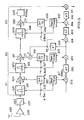
- Fig. 3 shows a further embodiment of a signal processing device in the form of a block diagram.
- the signal processing device is part of a receiver, for example.
- a received signal passes via an antenna 399 and an analog amplifier 398 and an analog-to-digital converter 397 as a digitized signal to a detection device 309, in the signal path three adjustable band pass filters 301, 305, 366, each with a multiplier 303, 307, 308 upstream ,
- Detector 309 is configured to detect a signal strength of the signal filtered by bandpass filters 301, 305, 366.
- the detector 309 is configured to output a detection value RSSI R representing the signal strength of the filtered signal,
- the digital filters 301, 305, 366 are configured to be adjustable, wherein filter coefficients for setting a transmission characteristic of the respective filter 301, 305, 366 are assigned to a gain or attenuation of the signal by the filter 301, 305, 366. Gain or attenuation can not usually be avoided to achieve a bandpass transfer function. By changing the transfer function, for example by changing the bandwidth of the respective filter 301, 305, 366, the gain or attenuation of the signal in the passband is forcibly changed in a predetermined manner, however.
- the multipliers are provided. If, for example, the attenuation through the filter is 1 / 4,2, a compensation by the factor 4 can be carried out by the multiplier, so that the total attenuation of the filter and multiplier is 4 / 4,2. Since the total attenuation is not equal to 1, the attenuation of the filter is only partially compensated, leaving a residual error.
- the multipliers 303, 307, 308 allow only gain or attenuation by a factor of 1 / (2 n ), where n is an integer.
- the inputs of the multipliers 303, 307, 308 are thus controlled exclusively with signals n1, n2, n3 for integers.
- a respective control signal s BW1 , BW2 , BW3 can be applied to a control terminal 325, 327 and 336, respectively.
- the control signal s BW1 causes a reading of the filter coefficients associated memory values n1 of the table T1 of the memory element 321.
- the control signal s BW1 causes a readout of correction values Rest1 from a table T1 (Id).
- the memory elements 321 and 317 can be individual memories or fixed or freely definable areas in a total memory (flash, etc.).
- the signal processing device has a correction device for applying the detection value to a correction value which at least partially compensates for the residual error.
- the correction device has in the embodiment of Fig. 3 an adder 311 for addition of logarithmic values.
- the detection value RSSI R of the detection device 309 is also logarithmic.
- the correction value Rest1 of the table T1 (Id) is also logarithmic and passes through the adder 313, the delay element 302 with the delay ⁇ 1, the adders 315 and 314, the delay element 304 with the delay ⁇ 2, the adder 316 and the delay element 332 with the Delay ⁇ 3 to the adder 311 of the correction device.
- the same integer Int is supplied as a negative value to the adder 314 and thus from the sum of the correction values Rest1 and Rest2 subtracted again.
- the adjustment of the coefficients of the filters 301, 305, 366 is preferably timed and / or dependent on a measured frequency offset of the signal from an expected center frequency, for which purpose the bandwidth of the respective filter 301, 305, 366 is reduced.
- the invention is not limited to the illustrated embodiments of FIGS. 1 to 3 limited. For example, it is possible to provide a larger number of filter stages.
Landscapes
- Cable Transmission Systems, Equalization Of Radio And Reduction Of Echo (AREA)
- Amplifiers (AREA)
- Control Of Amplification And Gain Control (AREA)
- Circuits Of Receivers In General (AREA)
- Networks Using Active Elements (AREA)
- Transmitters (AREA)
- Filters That Use Time-Delay Elements (AREA)
Applications Claiming Priority (1)
| Application Number | Priority Date | Filing Date | Title |
|---|---|---|---|
| DE102007024013A DE102007024013B8 (de) | 2007-05-22 | 2007-05-22 | Signalverarbeitungsvorrichtung und Signalverarbeitungsverfahren |
Publications (3)
| Publication Number | Publication Date |
|---|---|
| EP2001129A2 true EP2001129A2 (de) | 2008-12-10 |
| EP2001129A3 EP2001129A3 (de) | 2009-09-02 |
| EP2001129B1 EP2001129B1 (de) | 2010-02-03 |
Family
ID=39743787
Family Applications (1)
| Application Number | Title | Priority Date | Filing Date |
|---|---|---|---|
| EP08008707A Expired - Fee Related EP2001129B1 (de) | 2007-05-22 | 2008-05-09 | Signalverarbeitungsvorrichtung und Signalverarbeitungsverfahren |
Country Status (4)
| Country | Link |
|---|---|
| US (1) | US8107911B2 (is) |
| EP (1) | EP2001129B1 (is) |
| JP (1) | JP4658160B2 (is) |
| DE (2) | DE102007024013B8 (is) |
Families Citing this family (2)
| Publication number | Priority date | Publication date | Assignee | Title |
|---|---|---|---|---|
| US20090031485A1 (en) * | 2007-07-30 | 2009-02-05 | Robert Prusinski | Face Shield for Safety Helmet |
| EP2362544A1 (en) * | 2010-02-23 | 2011-08-31 | Alcatel Lucent | A signal amplifying component with gain compensation stages for compensating gain tolerances |
Citations (1)
| Publication number | Priority date | Publication date | Assignee | Title |
|---|---|---|---|---|
| US20060014508A1 (en) | 2002-09-25 | 2006-01-19 | Francois Seneschal | Device and method for determining the level of an input signal intended to be applied to a receiving system |
Family Cites Families (24)
| Publication number | Priority date | Publication date | Assignee | Title |
|---|---|---|---|---|
| US4226914A (en) | 1978-05-19 | 1980-10-07 | Ford Motor Company | Novel spraying composition, method of applying the same and article produced thereby |
| US4691722A (en) | 1984-08-01 | 1987-09-08 | Fsi Corporation | Bowl for liquid spray processing machine |
| DE4113211A1 (de) | 1991-04-23 | 1992-10-29 | Winfried Heinzel | Verfahren zum beschichten von haus- und kuechengeraetschaften |
| US6195399B1 (en) * | 1994-03-28 | 2001-02-27 | Ericsson Inc. | Method and apparatus for converting a wideband if signal to a complex (quadrature) baseband signal |
| JPH09199961A (ja) * | 1996-01-22 | 1997-07-31 | Oki Electric Ind Co Ltd | Agc装置 |
| US6240933B1 (en) | 1997-05-09 | 2001-06-05 | Semitool, Inc. | Methods for cleaning semiconductor surfaces |
| US6058148A (en) * | 1997-06-27 | 2000-05-02 | Ford Motor Company | Digital processing radio receiver with adaptive bandwidth control |
| US6240100B1 (en) * | 1997-07-31 | 2001-05-29 | Motorola, Inc. | Cellular TDMA base station receiver with dynamic DC offset correction |
| JPH11187463A (ja) * | 1997-12-24 | 1999-07-09 | Sony Corp | 移動体無線受信機 |
| JP2000278062A (ja) * | 1999-03-23 | 2000-10-06 | Nec Saitama Ltd | 自動利得制御回路 |
| US6654593B1 (en) * | 2000-10-30 | 2003-11-25 | Research In Motion Limited | Combined discrete automatic gain control (AGC) and DC estimation |
| DE10114779A1 (de) * | 2001-03-26 | 2002-10-24 | Infineon Technologies Ag | Sende-und Empfangseinheit |
| US6498927B2 (en) * | 2001-03-28 | 2002-12-24 | Gct Semiconductor, Inc. | Automatic gain control method for highly integrated communication receiver |
| US20030081706A1 (en) * | 2001-10-25 | 2003-05-01 | Ciccarelli Steven C. | Noise reduction filtering in a wireless communication system |
| US7299021B2 (en) * | 2001-12-28 | 2007-11-20 | Nokia Corporation | Method and apparatus for scaling the dynamic range of a receiver for continuously optimizing performance versus power consumption |
| JP3805258B2 (ja) * | 2002-01-29 | 2006-08-02 | 松下電器産業株式会社 | ダイレクトコンバージョン受信機 |
| JP3622728B2 (ja) * | 2002-01-30 | 2005-02-23 | 日本電気株式会社 | 受信機のベースバンド回路及びその低域遮断周波数制御方法 |
| US6760362B2 (en) * | 2002-03-15 | 2004-07-06 | Qualcomm Incorporated | Dynamic pilot filter bandwidth estimation |
| US7139542B2 (en) * | 2003-03-03 | 2006-11-21 | Nokia Corporation | Method and apparatus for compensating DC level in an adaptive radio receiver |
| US7295813B2 (en) * | 2003-07-30 | 2007-11-13 | Motorola Inc. | Current reduction by dynamic receiver adjustment in a communication device |
| EP1724937A1 (en) * | 2004-03-08 | 2006-11-22 | Matsushita Electric Industrial Co., Ltd. | Receiving circuit, and receiving apparatus and transmitting/receiving apparatus using the receiving circuit |
| US7556697B2 (en) * | 2004-06-14 | 2009-07-07 | Fsi International, Inc. | System and method for carrying out liquid and subsequent drying treatments on one or more wafers |
| JP4779523B2 (ja) * | 2005-09-14 | 2011-09-28 | 日本電気株式会社 | 受信電界強度検出回路及びその方法並びにそれを用いた受信機 |
| KR100788637B1 (ko) * | 2006-10-02 | 2007-12-26 | (주)에프씨아이 | 이득제어 및 다중대역의 처리가 가능한 수신기 |
-
2007
- 2007-05-22 DE DE102007024013A patent/DE102007024013B8/de not_active Withdrawn - After Issue
-
2008
- 2008-05-09 EP EP08008707A patent/EP2001129B1/de not_active Expired - Fee Related
- 2008-05-09 DE DE502008000354T patent/DE502008000354D1/de active Active
- 2008-05-22 JP JP2008134216A patent/JP4658160B2/ja not_active Expired - Fee Related
- 2008-05-22 US US12/125,087 patent/US8107911B2/en not_active Expired - Fee Related
Patent Citations (1)
| Publication number | Priority date | Publication date | Assignee | Title |
|---|---|---|---|---|
| US20060014508A1 (en) | 2002-09-25 | 2006-01-19 | Francois Seneschal | Device and method for determining the level of an input signal intended to be applied to a receiving system |
Also Published As
| Publication number | Publication date |
|---|---|
| DE502008000354D1 (de) | 2010-03-25 |
| DE102007024013B8 (de) | 2009-04-16 |
| JP2008295050A (ja) | 2008-12-04 |
| US20080293369A1 (en) | 2008-11-27 |
| EP2001129B1 (de) | 2010-02-03 |
| DE102007024013B3 (de) | 2008-11-27 |
| US8107911B2 (en) | 2012-01-31 |
| JP4658160B2 (ja) | 2011-03-23 |
| EP2001129A3 (de) | 2009-09-02 |
Similar Documents
| Publication | Publication Date | Title |
|---|---|---|
| DE102004005130B3 (de) | Sende-/Empfangsanordnung und Verfahren zur Reduktion von Nichtlinearitäten in Ausgangssignalen einer Sende-/Empfangsanordnung | |
| EP0707383B1 (de) | Schaltungsanordnung zur Analog-Digital-Wandlung von Signalen | |
| DE102009010155B4 (de) | Digitales Trimmen von (SAR-)ADCs | |
| EP2041897B1 (de) | Verfahren und anordnung zur kalibrierung von sendepfaden eines antennensystems | |
| DE60018114T2 (de) | Verfahren und gerät zur vorstufensignalverarbeitung für einen bildsensor | |
| DE69630461T2 (de) | Digitale eichung eines transceivers | |
| DE102014101705A1 (de) | Einstellbare Richtkopplerschaltung | |
| DE102004042779A1 (de) | Verfahren und System für eine Rauschreduktion bei Messempfängern unter Verwendung einer automatischen Rauschsubtraktion | |
| DE102005011916A1 (de) | Verfahren und Vorrichtung zur Kalibrierung des Gleichspannungs-Offset eines Digital/Analog-Wandlers | |
| DE102007006577B4 (de) | Signalverarbeitungssystem, das Signalpegel ändern kann | |
| DE69830451T2 (de) | System und Verfahren zur Kalibrierung nichtlinearer Verstärker | |
| EP2001129B1 (de) | Signalverarbeitungsvorrichtung und Signalverarbeitungsverfahren | |
| DE3044582C2 (de) | Digitaler Verstärker, insbesondere zur Verwendung in einer digitalen Fernsprech-Teilnehmerschaltung | |
| DE60217963T2 (de) | Vorwärtskopplungsverstärkungsschaltung | |
| DE60317135T2 (de) | Hochfrequenzsignalempfänger | |
| DE102020103724A1 (de) | Transimpedanzverstärker-übertragungsfunktionskompensation | |
| DE19631388C2 (de) | Verfahren zum Vorverzerren eines über eine nichtlineare Übertragungsstrecke zu übertragenden Signals und Schaltungsanordnung zum Durchführung des Verfahrens | |
| EP1168606A2 (de) | Vorrichtung und Verfahren zum Verabeiten von Hochfrequenzsignalen | |
| DE102011006566A1 (de) | Vorrichtungen zum automatischen Einstellen eines Verstärkungs- bzw. Dämpfungsfaktors | |
| EP2893654B1 (de) | Kalibriervorrichtung, signalverarbeitungsvorrichtung und benutzerschnittstelle für dieselbe | |
| DE10252099B4 (de) | Messgerät und Verfahren zum Ermitteln einer Kennlinie einer Hochfrequenzeinheit | |
| DE3408384C2 (de) | Schaltkreis zur Nachbildung einer Impedanz | |
| DE60315832T2 (de) | Empfangssignalpegelangabe | |
| DE19725171A1 (de) | Schaltungsanordnung zur Wandlung eines analogen Signals in ein digitales Signal | |
| DE102005012390B4 (de) | Verfahren zur Kompensation einer Verstärkungs-Fehlanpassung zwischen zwei Digital/Analog-Wandlern und korrespondierende Vorrichtung |
Legal Events
| Date | Code | Title | Description |
|---|---|---|---|
| PUAI | Public reference made under article 153(3) epc to a published international application that has entered the european phase |
Free format text: ORIGINAL CODE: 0009012 |
|
| 17P | Request for examination filed |
Effective date: 20080509 |
|
| AK | Designated contracting states |
Kind code of ref document: A2 Designated state(s): AT BE BG CH CY CZ DE DK EE ES FI FR GB GR HR HU IE IS IT LI LT LU LV MC MT NL NO PL PT RO SE SI SK TR |
|
| AX | Request for extension of the european patent |
Extension state: AL BA MK RS |
|
| PUAL | Search report despatched |
Free format text: ORIGINAL CODE: 0009013 |
|
| RAP1 | Party data changed (applicant data changed or rights of an application transferred) |
Owner name: ATMEL AUTOMOTIVE GMBH |
|
| AK | Designated contracting states |
Kind code of ref document: A3 Designated state(s): AT BE BG CH CY CZ DE DK EE ES FI FR GB GR HR HU IE IS IT LI LT LU LV MC MT NL NO PL PT RO SE SI SK TR |
|
| AX | Request for extension of the european patent |
Extension state: AL BA MK RS |
|
| GRAP | Despatch of communication of intention to grant a patent |
Free format text: ORIGINAL CODE: EPIDOSNIGR1 |
|
| GRAS | Grant fee paid |
Free format text: ORIGINAL CODE: EPIDOSNIGR3 |
|
| GRAA | (expected) grant |
Free format text: ORIGINAL CODE: 0009210 |
|
| AK | Designated contracting states |
Kind code of ref document: B1 Designated state(s): DE FR |
|
| REF | Corresponds to: |
Ref document number: 502008000354 Country of ref document: DE Date of ref document: 20100325 Kind code of ref document: P |
|
| AKX | Designation fees paid |
Designated state(s): DE FR |
|
| PLBE | No opposition filed within time limit |
Free format text: ORIGINAL CODE: 0009261 |
|
| STAA | Information on the status of an ep patent application or granted ep patent |
Free format text: STATUS: NO OPPOSITION FILED WITHIN TIME LIMIT |
|
| 26N | No opposition filed |
Effective date: 20101104 |
|
| REG | Reference to a national code |
Ref country code: FR Ref legal event code: ST Effective date: 20110131 |
|
| PG25 | Lapsed in a contracting state [announced via postgrant information from national office to epo] |
Ref country code: FR Free format text: LAPSE BECAUSE OF NON-PAYMENT OF DUE FEES Effective date: 20100531 |
|
| REG | Reference to a national code |
Ref country code: DE Ref legal event code: R082 Ref document number: 502008000354 Country of ref document: DE Representative=s name: GRUENECKER, KINKELDEY, STOCKMAIR & SCHWANHAEUS, DE Effective date: 20130529 Ref country code: DE Ref legal event code: R081 Ref document number: 502008000354 Country of ref document: DE Owner name: ATMEL CORP., US Free format text: FORMER OWNER: ATMEL AUTOMOTIVE GMBH, 74072 HEILBRONN, DE Effective date: 20130529 Ref country code: DE Ref legal event code: R081 Ref document number: 502008000354 Country of ref document: DE Owner name: ATMEL CORP., SAN JOSE, US Free format text: FORMER OWNER: ATMEL AUTOMOTIVE GMBH, 74072 HEILBRONN, DE Effective date: 20130529 Ref country code: DE Ref legal event code: R082 Ref document number: 502008000354 Country of ref document: DE Representative=s name: GRUENECKER PATENT- UND RECHTSANWAELTE PARTG MB, DE Effective date: 20130529 |
|
| PGFP | Annual fee paid to national office [announced via postgrant information from national office to epo] |
Ref country code: DE Payment date: 20190418 Year of fee payment: 12 |
|
| REG | Reference to a national code |
Ref country code: DE Ref legal event code: R119 Ref document number: 502008000354 Country of ref document: DE |
|
| PG25 | Lapsed in a contracting state [announced via postgrant information from national office to epo] |
Ref country code: DE Free format text: LAPSE BECAUSE OF NON-PAYMENT OF DUE FEES Effective date: 20201201 |