EP2000949A2 - Kartenverbinder - Google Patents
Kartenverbinder Download PDFInfo
- Publication number
- EP2000949A2 EP2000949A2 EP08251902A EP08251902A EP2000949A2 EP 2000949 A2 EP2000949 A2 EP 2000949A2 EP 08251902 A EP08251902 A EP 08251902A EP 08251902 A EP08251902 A EP 08251902A EP 2000949 A2 EP2000949 A2 EP 2000949A2
- Authority
- EP
- European Patent Office
- Prior art keywords
- card
- open
- close cover
- holding cavity
- housing
- Prior art date
- Legal status (The legal status is an assumption and is not a legal conclusion. Google has not performed a legal analysis and makes no representation as to the accuracy of the status listed.)
- Withdrawn
Links
Images


Classifications
-
- G—PHYSICS
- G06—COMPUTING OR CALCULATING; COUNTING
- G06K—GRAPHICAL DATA READING; PRESENTATION OF DATA; RECORD CARRIERS; HANDLING RECORD CARRIERS
- G06K7/00—Methods or arrangements for sensing record carriers, e.g. for reading patterns
- G06K7/0013—Methods or arrangements for sensing record carriers, e.g. for reading patterns by galvanic contacts, e.g. card connectors for ISO-7816 compliant smart cards or memory cards, e.g. SD card readers
- G06K7/0021—Methods or arrangements for sensing record carriers, e.g. for reading patterns by galvanic contacts, e.g. card connectors for ISO-7816 compliant smart cards or memory cards, e.g. SD card readers for reading/sensing record carriers having surface contacts
Definitions
- the present invention relates to card connectors having a connector housing, contact terminals and an open - closer that opens portions of the connector housing and holding cavity.
- Embodiments of the present invention can provide card connectors that are installed and used in various electronic equipment such as personal computers and portable terminals. More particularly, embodiments of the present invention can provide card connectors into which small-size cards such as memory cards of differing outer-dimension size and thickness can be inserted.
- card connectors have been used for insertion of small-size cards, etc., with built-in CPU or memory IC, etc., such as micro MMCs (multi media cards) or micro SD (super density) cards, so as to expand the capabilities of such equipment.
- micro MMCs multi media cards
- micro SD super density
- a typical example of such a card connector is set forth in JP-A-2003-197296 .
- This card connector has a connector housing with a card insertion aperture at the front and a card holding cavity inside, and multiple contact terminals that are fitted in the inner part of the card holding cavity; the structure is such that two card types of differing size and thickness can be inserted through the insertion aperture. Also, a card sensing switch is provided in the housing, and the installation status of each card type can be sensed.
- FIG. 614 Another typical example of a card connector is set forth in US Patent No. 6,642,614 .
- This connector has a connector housing provided with a card holding cavity whose front and top are open; multiple contact terminals that are fitted in the inner part of the card holding cavity; and a covering that covers the top opening of the connector housing; the structure is such that two card types of differing size and thickness can be inserted through the front opening.
- an insertion aperture is formed in the front of the connector housing, two card types of differing size and thickness can be inserted through the insertion aperture, and the cards' contacts are electrically connected to the connector's contact terminals.
- the connector set forth in JP-A-2003-197296 is provided with a sensing switch that senses the card installation status, and is therefore able to sense adequate installation status. But the above trial-and-error connection operations will still have to be carried out until adequate installation is effected, which means that the above problems will remain.
- the card connector set forth in US Patent No. 6,642, 614 although facilitating formation of the card holding cavity by having the top opening covered by a covering, has the same problems in the assembled state, because the covering is joined to the connector housing by means of bonding agent or the like.
- these card connectors are common connectors that are used with cards of differing thickness, which means that the distance between the contacts of the various cards and the connector's contact terminals will vary with the difference in thickness.
- the resilience of the contact terminals has been adjusted to match a thick card, it will not be possible to impart the requisite resilience to the contact terminals with a thin card; and conversely, when the resilience of the contact terminals has been adjusted to match a thin card, then with a thick card the contact terminals will be excessively displaced, exceed their stress limit, and undergo plastic deformation.
- the card holding cavity is formed to a size that matches large-sized, thick cards. Consequently, when a small-sized, thin card is housed in the card holding cavity, which is suited for a large-sized card, gaps equivalent to the differences in the size and thickness of the two card types will occur inside the card holding cavity. Because of this, the small-sized, thin card will be housed in an unstable condition inside the card holding cavity, and will move readily if some impact acts on the connector, possibly resulting in poor connection between the card and connector, and hence in failure.
- An advantage of some aspects of the present invention is to provide a card connector which permits the interior of the card holding cavity to be examined when a card is housed therein, and into which cards of differing size and thickness can be installed more reliably, in a more simple manner, and with card misinstallations eliminated or at least reduced.
- a card connector of the present invention includes: a connector housing constituted of electrical insulators and capable of housing cards inside a bottomed card holding cavity which is formed therein so as to be enclosed on three sides by an opposed pair of first and second frames and a third frame that links the end portions of the first and second frames, and so as to be open at the front and top; contact terminals that are deposed inside the connector housing's card holding cavity; and an open-close cover that covers the open portions of the connector housing's card holding cavity.
- the card connector has the features that: the open-close cover has, at the front thereof where the card is installed, a sensing member that senses the installation status of the card; the rear of the open-close cover is rotatably pivoted on the first and second frames; and after a card is installed inside the card holding cavity, the card's installation status is sensed by closing the open-close cover and positioning the sensing member of the open-close cover at the rear end portion of the card.
- the card holding cavity may be formed in a shape that permits cards of differing size and thickness to be housed therein, the contact terminals that contact with the contacts of such cards being installed inside the card housing cavity.
- the card holding cavity may be formed in a shape that permits a first and a second card type of differing size and thickness to be housed therein, with the contact terminals including first and second contact terminals that are provided inside the card holding cavity and contact with the contacts of the first and second card types respectively.
- Such first contact terminals may be fixed to the third frame of the connector housing, and such second contact terminals be fixed to the bottom of the connector housing.
- the open-close cover may be formed from metal plates including a pair of first and second sideplates that cover the outer side surfaces of the first and second frames, a top plate that links the top edges of the sideplates and covers the upper opening of the card holding cavity, and a front cover plate that covers the front opening of the card holding cavity, with the front cover plate serving as the sensing member.
- Either the first or the second frame of the connector housing may be provided with a first switch means that senses the installation status of the card, and with a second switch means that senses the open/closed status of the open-close cover.
- Such first switch means may be composed of a first fixed contact terminal having a fixed contact, and a first movable contact terminal having a movable contact that contacts and separates from the fixed contact, together with an actuating part that separates the movable contact from the fixed contact as a card is installed; and such second switch means may be composed of a second fixed contact terminal having a fixed contact, and a second movable contact terminal having a movable contact that contacts and separates from the fixed contact, together with an actuating protrusion that separates the movable contact from the fixed contact in interlock with opening/closing manipulation of the open-close cover.
- the actuating protrusion of such second movable contact terminal may, in interlock with closing manipulation of the open-close cover, cause the second switch means to execute a series of OFF-ON-OFF operations; in the final OFF state, the actuating protrusion will be latched into a latching hole provided in the frame, thereby locking the open-close cover in the closed state.
- An aperture portion for insertion of the leading end of the first card type, which is long compared to the second card type, may be formed in the third frame; so that as a first card type is installed, the leading end of the first card type will be inserted into such aperture and thereby be positioned and secured.
- the open-close cover of a card connector is opened when a card is installed, so that, in this opened state, the interior of the card holding cavity can be examined.
- the sensing member will strike against the trailing end portion of the card so that closing of the cover will not be possible, and incomplete connection of the connector and card will thereby be eliminated.
- the card holding cavity is formed in a shape that can hold cards of differing size and thickness, and moreover, contact terminals for contacting with the cards' contacts are installed inside the card holding cavity, so that the card connector can be used as a common connector for multiple card types of differing size and thickness.
- the card connector can be used for two card types of differing size and thickness, for example, for micro SD cards and micro MM cards.
- the open-close cover is formed from metal plates including a pair of first and second sideplates that cover the outer side surfaces of the first and second frame, a top plate that links the top edges of the sideplates and covers the upper opening of the card holding cavity, and a front cover plate that covers the front opening of the card holding cavity, with the front cover plate serving as the sensing member; thanks to which, the open-close cover can be manufactured in a simple manner, by punching out plate metal of the requisite thickness and performing metal plate processing thereon.
- the front cover plate serves as the sensing member and the front opening of the card holding cavity will be covered over when the open-close cover is close, entry of dust or the like into the card holding cavity interior will be prevented or at least reduced, and a stable connected state can be maintained. What is more, because it is formed of metal plates, the open-close cover will, when installed to the connector housing, electromagnetically shield the connector.
- a first switch means whether or not a card has been installed in the regular state can be sensed in a simple manner, and thanks to a second switch means, the open/closed status of the open-close cover can be sensed; as a result, it is possible to proactively prevent incomplete installation of the card and incomplete closing of the open-close cover.
- the open/closed status of the open-close cover can be sensed, and moreover, the open-close cover can be locked.
- the leading end of the first card type when a first card type is installed, the leading end of the first card type will be inserted into an aperture portion formed in the third frame and thereby be positioned and secured.
- the first card type since the first card type will be positioned via positioning by the guide member, as well as via insertion into this aperture portion, the card will be accurately positioned and secured inside the card holding cavity.
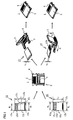
- a card connector (below, "connector") 1 is used with two types of card, a first type and a second type, that differ slightly in size and thickness, for instance a micro SD (super density) card 13 and a micro MM (multi media) card 15. Accordingly, outline descriptions of these cards will first be given.
- the micro SD card 13 includes a rectangular plate-like body having longitudinal length L 1 , widths W 1 and W 2 at the forward and rear end portions 13a and 13b (W 1 ⁇ W 2 ), and thickness t 1 .
- the interior thereof contains an IC chip, while the outer periphery is formed from a molding of electrically insulative synthetic resin.
- On one of the side edges (the first side edge) 13 1 of this micro SD card 13 there are provided a positioning protrusion 13c and a latching indent 13e, while the other side edge 132 is a straight line.
- On the obverse face of the micro SD card 13 there are provided multiple contacts 13d that are connected to the IC chip in the interior.
- the micro MM card 15 has almost the same shape as the micro SD card 13, including a molding having longitudinal length L 2 , widths W 3 and W 4 at the forward and rear end portions 15a and 15b (W 3 ⁇ W 4 ), and thickness t 2 .
- the micro MM card 15 too has a positioning protrusion 15c provided in one of the side edges (the first side edge) 15 1 , the other side edge (the second side edge) 15 2 being a straight line, and has multiple contacts 15d provided on its obverse face. Moreover, the contacts 13d, 15d are provided on the reverse sides of the cards 13, 15 shown in Fig. 1 , being indicated by dashed lines therein.
- the relations between the widths, lengths and thicknesses of these micro SD and micro MM cards 13, 15 are: W 3 > W 1 , L 1 > L 2 , and t 2 > t 1 .
- the connector 1 has: a connector housing (below, the "housing") 2 with a card holding cavity 24 in which the micro SD or micro MM card 13, 15 are installed; first and second contact terminals 5, 6 that are housed in the housing 2 and are electrically connected to the contacts 13d, 15d of the respective card; and an open-close cover 3 and shield cover 4 which are mounted on top of the housing 2.
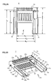
- Figs. 3 and 4 give perspective views of the housing 2 seen from different angles, to facilitate comprehension of the structure of the housing 2.
- the housing 2 is formed as an electrically insulative synthetic resin molding, which is surrounded by an opposed pair of first and second frames 21, 22 and a third frame that links the end portions of the first and second frames 21, 22, and which has a shallow-bottomed card holding cavity 24 that is open on three sides - the front, the top, and part of the bottom.
- the upper surface of the housing 2 is partitioned, part-way along from the front end toward the rear, into two: an open-close cover mounting part i toward the front, that is covered by the open-close cover 3, and a shield cover mounting part ii toward the rear, where the shield cover 4 is mounted.
- the pair of first and second frames 21, 22 are provided so as to have a spacing therebetween slightly larger than the larger width W 4 of the micro MM card 15, have a length slightly longer than the length L 1 of the longer micro SD card 13, and are formed as square pillar-like bodies of a particular thickness. More precisely, as shown in Figs. 3B and 4A , the first frame 21 is formed as a square-pillar body having obverse and reverse wall faces 21 A , 21 B and inner and outer wall faces 21c, 21 D . Likewise, the second frame 22 is formed as a square-pillar body having obverse and reverse wall faces 22 A , 22 B and inner and outer wall faces 22c, 22 D . Further, the third frame 23 too is formed as a square-pillar body of a particular thickness, which has obverse and reverse wall faces 23 A , 23 B and inner and outer wall faces 23c, 23 D .
- the first frame 21 is a little thicker than the second frame 22, and as shown in Figs. 3B and 4B , is provided with first and second switch mounting portions S1, S2 at two locations, toward the front and the rear.
- a switch member for sensing the installation status of the micro SD and micro MM cards 13, 15 is fitted into the first switch mounting portion S1
- a switch member for sensing the open-closed status of the open-close cover 3 is fitted into the second switch mounting portion S2.
- the first switch mounting portion S1 is composed, as shown in Fig. 3B , of a square-bottomed depression 21 1 that is cut out, at a particular depth, from the obverse wall face 21 A toward the reverse wall face 21 B of the first frame 21; and two mounting slots 21 2 ,- 21 3 that communicate with the square-bottomed depression 21 1 , these being provided in the vicinity of the third frame 23.
- the bottom of the square-bottomed depression 21 1 includes a platform 21 E that is higher by a particular height h than the inner bottom plate 25 A to be described later.
- This platform 21 E is the same height as a lateral bottom plate 25 C' to be described later, and the thick micro MM card 15 is supported in parallel by the platform 21 E and the lateral bottom plate 25 C' .
- the mounting slot 21 2 is formed on the obverse wall face 21 A of the first frame 21, and has a width that allows insertion of a movable contact terminal 7 to be described later.
- In the reverse wall face 21 B of the first frame 21 there is formed an insertion slot 21 2' into which the fitting tab 7 E of the movable contact terminal 7 is inserted (see Fig. 4B ).
- the mounting slot 21 3 is formed in the reverse wall face 21 B of the first frame 21 and has a width that allows insertion of a fixed contact terminal 8 to be described later.
- the second switch mounting portion S2 is formed, as shown in Fig. 4 , with a square-bottomed depression 21 4 that sinks to a particular depth from the outer wall face 21 D of the first frame 21; and two mounting slots 21 5 , 21 6 that communicate with the square-bottomed depression 21 4 .
- a switch member for sensing the open/closed status of the open-close cover 3 is fitted into the second switch mounting portion S2.
- the front portion of the outer wall face 21 D of the first frame 21 bulges outward, while the rear portion thereof that is close to the third frame 23 includes a flat surface 21 D' that lies beyond a step difference, being recessed relative to the front portion, and in such flat surface 21 D' there is formed a latching protrusion 21 P onto which the shield cover 4 latches.
- width dimension W H4 between the front portion of the inner wall face 21 C of the first frame 21 and the inner wall face 22 C of the second frame 22, which is opposed to the inner wall face 21c.
- the positioning protrusion 13c or 15c of the micro SD or micro MM card 13 or 15 will strike against the inclined face 21 C' , blocking any further pushing-in of the card, so that wrong installation is prevented.
- the inclined face 21 C' will serve as a guide surface that renders the pushing-in smooth.
- a mounting slot 21 T In the front portion of the reverse wall face 21 B of the first frame 21 there is formed a mounting slot 21 T into which a fitting tab is fitted.
- the front portion of the outer wall face 22 D of the second frame 22 bulges outward, while the rear portion thereof that is close to the third frame 23 includes a flat surface 22 D' that lies beyond a step difference, being recessed relative to the front portion, and in such flat surface 22 D' there is formed a latching protrusion 22 P onto which the shield cover 4 latches.
- a mounting slot 22 T In the front portion of the outer wall face 22 D of there is formed a mounting slot 22 T into which a fitting tab fits.
- the aperture 23 2 is formed with a longitudinal dimension a little larger than the width W 1 of the micro SD card 13 and with a height a little larger than the thickness t 1 of the micro SD card 13, so that when the leading end portion 13a of the micro SD card 13 is inserted into the aperture, positioning and securing of the micro SD card 13 is effected.
- the first and second frames 21, 22 are coupled via a bottom plate 25 extending from the third frame 23 toward the front portions of the first and second frames 21, 22. More precisely, the reverse wall faces 21 B , 22 B of the first and second frames 21, 22 are coupled via a bottom plate 25 of a particular thickness.
- This bottom plate 25 is formed as an inner bottom plate 25 A that couples the two frames 21, 22, plus lateral bottom plates 25 B , 25 C that are drawn out from the inner bottom plate 25 A and divided along the first and second frames 21, 22.
- One lateral bottom plate, 25 C has its portion adjacent to the second frame 22 formed as a lateral bottom plate 25 C' that is higher by a particular height h. Also, in the inner bottom plate 25 A there are formed, with roughly equal spacings, multiple mounting slots 25 1 into which the second contact terminals 6 are installed.
- the card holding cavity 24 is formed by being surrounded on three sides by the first and second frames 21, 22 plus the third frame 23.
- the distance W H4 between the inner wall faces 21c, 22c of the first and second frames 21, 22, and the distance W H3 between the inner wall face 22c and the inclined face 21 C' are formed to be a little larger than the widths W 4 , W 3 of the micro MM card 15, so that the broad micro MM card 15 can be inserted.
- the length L H1 from the leading end portion to the interior of the aperture 23 2 is formed to be almost equal to the length L 1 of the micro SD card 13, so that the micro SD card 13 can be inserted.
- the length L H2 from the leading end portion to the inner wall face 23c of the third frame 23 is formed to be almost equal to the length L 2 of the micro MM card 15.
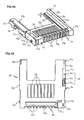
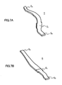
- the open-close cover 3, which is for covering the card holding cavity 24 of the housing 2, has, as Fig. 5 shows, a top plate 31 that covers the top opening of the card holding cavity 24; a pair of sideplates 32, 33 that are bent downward from the two side edges of the top plate 31 and cover the side wall faces of the housing 2; and a front cover plate 34 that similarly is bent downward from the front edge of the top plate 31 and covers the front opening of the card holding cavity 24; and is formed via punching of metal plate and bending processing.
- the front cover plate 34 serves as a sensing member that senses inappropriate installation status of the cards. Gaps 34 1 , 34 1 are formed between the two sideplates 32, 33 and the front cover plate 34.
- the pair of sideplates 32, 33 are extended a certain distance rearward, and on the ends of these extension portions 32 A , 33 A there are provided pivot protrusions 32 1 , 33 1 that each project toward the opposing sideplate surface.
- These extension portions 32 A , 33 A possess resilience and, during installation of the open-close cover 3 to the housing 2, will press against and be clasped by the sideplates 42, 43 of the shield cover 4 that is fitted to the side wall faces of the housing 2. Being formed of metallic material, when installed to the housing 2 the open-close cover 3 will act as an electromagnetic shielding member that shields the connector.
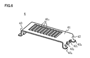
- the shield cover 4 which as Fig. 6 shows, is an item that is fitted to the shield cover mounting part ii of the housing 2, has a top plate 41 that covers over such mounting part, and a pair of sideplates 42, 43 that are bent downward from the two ends of the top plate 41; and is formed via punching of metal plate and bending processing.
- Multiple slits 41 1 are formed with roughly equal spacings in the top plate 41. Such spacings correspond to the first contact terminals 5 that are installed in the housing 2, and the width of the slits 41 1 is a dimension such that the first contact terminals 5 and the shield cover 4 will not contact.
- the sideplate 42 is provided with a latching hole 42 1 into which the latching protrusion 21 P of the housing 2 latches, a pivoting hole 42 2 in which the pivot protrusion 32 1 of the open-close cover 3 pivots, and a pair of fitting tabs 42 A , 42 A that fit into a circuit board such as a printed wiring board.
- the other sideplate 43 is also provided with a similar latching hole, pivoting hole and fitting tabs (omitted from the drawing).
- the sideplates 42, 43 possess resilience and, during installation to the housing 2, will press against and be clasped by the sidewall faces 21 D ', 22 D ' of the housing 2. Also, due to being formed from metallic material, when installed to the housing 2 the shield cover 4 will act as an electromagnetic shielding member that shields off external noise.
- Fig. 7 shows the first and second contact terminals 5 and 6.
- the first contact terminal 5 has at one end a contact 5 A that contacts with the contacts 15d of the micro MM card 15; at the other end a connecting portion 5 B that is connected by soldering to a lead wire; and, provided in the vicinity of the connecting portion 5 B , a fixing portion 5c for fixing to the housing 2; and is formed as a highly conductive, resilient strip-like metal piece of a particular width, length and thickness.
- the first contact terminal 5 is fitted to the third frame 23 of the housing 2, and electrically connected to the contacts 15d of the micro MM card 15.
- the second contact terminal 6 has at one end a contact 6 A that is electrically connected to the contacts 13d of the micro SD card 13; at the other end a connecting portion 6 B that is connected by soldering to a lead wire; and, provided in the vicinity of the connecting portion 6 B , a fixing portion 6c for fixing to the housing 2; and is formed as a highly conductive, resilient strip-like metal piece of a particular width, length and thickness.
- the second contact terminal 6 is fitted to the inner bottom plate 25 A of the housing 2, and connected to the contacts 13d of the micro SD card 13.
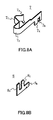
- Fig. 8 shows the first switch member that constitutes the first switch means SW 1 .
- This first switch means SW 1 is composed of a movable contact terminal 7 with a movable contact, and a fixed contact terminal 8 with a fixed contact.
- the movable contact terminal 7 has a movable contact 7 A provided at the front tip; a projecting curved portion 7c that is provided at a point somewhat removed from such contact and contacts against the first side edge 13 1 or 15 1 of the card 13 or 15; a curved portion 7 D that imparts resilience to the movable contact 7 A and projecting curved portion 7 C ; a connecting portion 7 B that is provided at the rear tip and is connected by soldering to a lead wire; and, provided in the vicinity of the connecting portion 7 B , a fitting tab 7 E that is fixed to the housing 2; and is formed as a highly conductive, resilient strip-like metal piece of a particular width, length and thickness.
- the projecting curved portion 7c serves as the actuating part for the first switch means SW 1 .
- the fixed contact terminal 8 has a fixed contact 8 A provided at the front tip; a connecting portion 8 B that is provided at the rear tip and is connected by soldering to a lead wire; and, provided in the vicinity of the connecting portion 8 B , a fitting tab 8c that is fixed to the housing 2; and is formed as a highly conductive, resilient strip-like metal piece of a particular width, length and thickness.
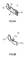
- Fig. 9 shows the second switch member that constitutes the second switch means SW 2 .
- This second switch means SW 2 is composed of a movable contact terminal 9 with a movable contact, and a fixed contact terminal 10 with a fixed contact.
- the movable contact terminal 9 has a latching protrusion 9 A provided at the front tip; a movable contact 9c provided in the vicinity of the latching protrusion 9 A ; a connecting portion 9 B that is connected by soldering to a lead wire; and, provided in the vicinity of the connecting portion 9 B , a fitting tab 9 D that is fixed to the housing 2; and is formed as a highly conductive, resilient strip-like metal piece of a particular width, length and thickness.
- the latching protrusion 9 A contacts against the inner face of the sideplate 32 of the open-close cover 3, and performs the function of causing the movable contact 9c of the movable contact terminal 9 to contact with the fixed contact 10 A of the fixed contact terminal 10, as well as that of locking the open-close cover 3.
- the fixed contact terminal 10 has a fixed contact 10 A provided at the front tip; a connecting portion 10c that is connected by soldering to a lead wire; and, provided in the vicinity of the connecting portion 10c, a fitting tab 10 B that is fixed to the housing 2; and is formed as a highly conductive, resilient strip-like metal piece of a particular width, length and thickness.
- Fig. 10 shows a pair of fitting tabs.
- These fitting tabs includes a left and a right fitting tab, 11 L and 11 R , are mounted to the bottom of the housing 2, and are for fixing the connector 1 to a circuit board such as a printed wiring board.
- the left fitting tab 11 L has a housing fixing portion 11 1 that is inserted into installation holes in the housing 2, and a circuit board fixing portion 11 2 that is drawn out from one end of the housing fixing portion 11 1 and is fixed to the circuit board by solder; and is formed as an approximately L-shaped metallic piece.
- the other, right fitting tab 11 R likewise has a housing fixing portion 11 1 and a circuit board fixing portion 11 2 .
- the left and right fitting tabs 11 L , 11 R differ in the direction in which the circuit board fixing portion 11 2 is drawn out relative to the housing fixing portion 11 1 .
- the first and second contact terminals 5, 6 shown in Fig. 7 are fitted to the housing 2 shown in Figs. 3 and 4 .
- the first contact terminals 5 are fitted by press-fitting and securing the fixing portions 5c thereof into the mounting slots 23 1 in the third frame 23 of the housing 2.
- the contacts 5 A of the first contact terminals 5 will be positioned inside the card housing cavity 24, while the connecting portions 5 B thereof will be in a state such as to project to the rear of the third frame 23, as shown in Fig. 12B .
- the second contact terminals 6 are fitted into the mounting slots 25 1 in the inner bottom plate 25 A .
- the second contact terminals 6 are fitted by passing the fixing portions 6c thereof along the back surface of the inner bottom plate 25 A , and insert-molding the fixing portions 6c through the mounting slots 25 1 so as to point upward and be secured.
- the contacts 6 A of the second contact terminals 6 will be positioned inside the card housing cavity 24, while the connecting portions 6 B thereof will be in a state such as to project to the lower surface of the inner bottom plate 25 A , as shown in Fig. 12B .
- first and second switch members shown in Figs. 8 and 9 are fitted to the first and second switch-mounting portions S1, S2 of the housing 2.
- the movable contact terminal 7 and the fixed contact terminal 8 are inserted into and fixed in mounting slot 21 2 and mounting slot 21 3 respectively.
- the movable contact terminal 9 and the fixed contact terminal 10 are inserted into and fixed in mounting slot 21 5 and mounting slot 21 6 respectively.
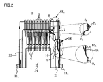
- Such fitting of the first and second switch members to the first and second switch mounting portions S1, S2 results in the formation of the first and second switch means SW 1 and SW 2 shown in Fig. 2 .
- the first switch means SW 1 is formed when the movable contact 7 A of the movable contact terminal 7 contacts with the fixed contact 8 A of the fixed contact terminal 8, and the projecting curved portion 7c projects inside the card holding cavity 24; while the second switch means SW 2 , is formed when the movable contact 9c of the movable contact terminal 9 faces, but is separated, i.e. disconnected from, the fixed contact 10 A of the fixed contact terminal 10, and the latching protrusion 9 A projects outward.
- the shield cover 4 shown in Fig. 6 is fitted to the shield cover mounting part ii at the rear of the housing 2.
- the shield cover 4 is fitted by pushing outward the two opposed sideplates 42, 42, against the resilience thereof, so that the distance therebetween is widened; bringing the two sideplates into contact with the sidewalls 21 D' , 22 D' of the housing 2, and mating the mating holes 42 1 , 43 1 of the two sideplates 42, 43 to the latching protrusions 21 P , 22 P on the housing 2, so as to effect fixing.
- the open-close cover 3 shown in Fig. 5 is fitted to the shield cover 4.
- the extension portions 32 A , 33 A of the two sideplates of the open-close cover 3 are pushed outward, against the resilience of the two sideplates, and fitting the pivot protrusions 32 1 , 33 1 provided in the extension portions into the pivoting holes 42 2 in the shield cover 4 so as to be secured but freely rotatable therein.
- the open-close cover 3 With the open-close cover 3 thus fitted to the housing 2, the open-close cover 3 can be opened/closed as desired, and when the open-close cover 3 is open, it is possible to examine the interior of the card holding cavity 24, as shown in Fig. 11 . After that, the left and right fitting tabs 11 L , 11 R shown in Fig. 10 are fitted into the mounting slots 21 T , 22 T in the bottom of the housing 2, whereupon assembly of the connector 1 is complete.
- the assembled connector 1 is used by being fitted to a printed wiring board or the like, which is not shown in the drawings.
- the open-close cover 3 is opened. Opening the open-close cover 3 exposes the interior of the card holding cavity 24, so that the interior is observable.
- a check is made by comparing the contacts 15d and positioning protrusion 15c of the micro MM card 15 to be inserted with the array status and hole shapes of the first contact terminals 5 inside the card holding cavity 24. Based on the result of such check, the micro MM card 15 shown in Fig. 1 is oriented with the contacts 15d on the upward face. Should the obverse and reverse faces of the micro MM card be the wrong way around, they will be changed so that the contacts 15d point upward.
- the micro MM card 15's first side edge 15 1 where the positioning protrusion 15c is provided, and reverse face, are brought into contact with the inner wall face 21c of the first frame 21 and the lateral bottom plate 25 B' of the card holding cavity 24, respectively, while at the same time the second side edge 15 2 is brought into contact with the lateral bottom plate 25c and inner wall face 22c of the second frame 22, and the card is inserted.
- the micro MM card 15's leading end portion 15a approaches the aperture 23 2
- the micro MM card 15 runs onto the platform 21 E , and the micro MM card 15's first side edge 15 1 contacts against the projecting curved portion 7c of the movable contact terminal 7.
- the projecting curved portion 7c of the movable contact terminal 7 is pushed outward, the movable contact 7 A of the movable contact terminal 7 becomes detached from the fixed contact 8 A of the fixed contact terminal 8, and the first switch means SW 1 is turned OFF.
- the fact that the micro MM card 15 has been installed can be sensed electrically via such turning OFF of the first switch means SW 1 (see Fig. 2 ).
- the open-close cover 3 is closed. If the micro MM card 15 has not been inserted up to the correct position at the time of such closing manipulation, the trailing end portion 15b of the micro MM card 15 will spring out to the exterior through the front opening of the card holding cavity 24, as shown in Fig. 11A . As a result, the front cover plate 34 of the open-close cover 3 will strike against the sprung-out portion and it will not be possible to close the open-close cover 3. Hence, incomplete installation of the micro MM card 15 can be sensed in a simple manner via such colliding of the open-close cover 3 with the micro MM card 15.
- the micro MM card 15 is inserted up to the regular position, it becomes possible to close the open-close cover 3, and the open-close cover 3 is closed.
- the front cover plate 34 covers the front opening, so that entry of dust or other foreign matter is prevented.
- the second switch means SW 2 executes a series of OFF-ON-OFF operations. More precisely, prior to closing of the open-close cover 3, the second switch means SW 2 is in the OFF state (see (B1) in Fig. 11B ). Then in the initial stage of closing of the open-close cover 3, the inner wall face of the open-close cover 3's sideplate 32 contacts against the latching protrusion 9 A of the second switch means SW 2 , the latching protrusion 9 A is pushed inward, and the second switch means SW 2 switches from OFF to ON (see (B2) in Fig. 11B ). At the same time, the latching protrusion 9 A enters into the mating hole 32 2 provided in the sideplates 32, 33 of the open-close cover 3, locking the open-close cover 3 in the closed state (see (B3) in Fig. 11B ).
- the micro SD card 13 Before the micro SD card 13 is installed inside the card holding cavity 24, the open-close cover 3 is opened. Since the interior of the card holding cavity 24 is exposed when the open-close cover 3 is opened, installation of the micro SD card 13 is carried out with roughly the same process as for installation of the micro MM card 15. More precisely, the micro SD card 13 is inserted by bringing the side edge 13 1 (first side edge), on which the positioning protrusion 13c is provided, into contact with the inner wall face 21c of the first frame 21, and the reverse face into contact with the lateral bottom plate 25 B of the card holding cavity 24, and at the same time bringing the second side edge 13 2 into contact with the lateral bottom plate 25c and inner wall face 22c of the second frame 22. Through such insertion, the micro SD card 13's leading end portion 13a enters into the aperture 23 2 and is thereby positioned and secured.
- the micro SD card 13's first side edge 13 1 contacts against and pushes outward the projecting curved portion 7c of the movable contact terminal 7, so that the movable contact 7 A of the movable contact terminal 7 is detached from the fixed contact 8 A of the fixed contact terminal 8 and the first switch means SW 1 is turned OFF.
- the fact that the micro SD card 13 has been installed can be sensed electrically via such turning OFF of the first switch means SW 1 .
- the open-close cover 3 is closed. Such closing manipulation is carried out with the same process as for installation of the micro MM card 15.
- the card connector 1 although described in the foregoing embodiment as being for use with a micro SD card 13 and a micro MM card 15, is not limited to being used with such cards.
Landscapes
- Engineering & Computer Science (AREA)
- Artificial Intelligence (AREA)
- Computer Vision & Pattern Recognition (AREA)
- Physics & Mathematics (AREA)
- General Physics & Mathematics (AREA)
- Theoretical Computer Science (AREA)
- Coupling Device And Connection With Printed Circuit (AREA)
- Details Of Connecting Devices For Male And Female Coupling (AREA)
- Connector Housings Or Holding Contact Members (AREA)
Applications Claiming Priority (1)
| Application Number | Priority Date | Filing Date | Title |
|---|---|---|---|
| SG200704178-3A SG148875A1 (en) | 2007-06-08 | 2007-06-08 | Card connector |
Publications (1)
| Publication Number | Publication Date |
|---|---|
| EP2000949A2 true EP2000949A2 (de) | 2008-12-10 |
Family
ID=39673428
Family Applications (1)
| Application Number | Title | Priority Date | Filing Date |
|---|---|---|---|
| EP08251902A Withdrawn EP2000949A2 (de) | 2007-06-08 | 2008-05-30 | Kartenverbinder |
Country Status (5)
| Country | Link |
|---|---|
| US (1) | US20080305665A1 (de) |
| EP (1) | EP2000949A2 (de) |
| JP (1) | JP5030840B2 (de) |
| CN (1) | CN101364695A (de) |
| SG (1) | SG148875A1 (de) |
Cited By (1)
| Publication number | Priority date | Publication date | Assignee | Title |
|---|---|---|---|---|
| CN103945022A (zh) * | 2013-01-17 | 2014-07-23 | 三星电子株式会社 | Sim卡座和包括该sim卡座的终端装置 |
Families Citing this family (4)
| Publication number | Priority date | Publication date | Assignee | Title |
|---|---|---|---|---|
| SG148874A1 (en) * | 2007-06-08 | 2009-01-29 | Mea Technologies Pte Ltd | Card connector |
| SG148876A1 (en) * | 2007-06-08 | 2009-01-29 | J S T Mfg Co Ltd | Card connector |
| CN102035069A (zh) * | 2009-09-30 | 2011-04-27 | 深圳富泰宏精密工业有限公司 | 便携式电子装置 |
| CN110635272B (zh) * | 2019-10-09 | 2025-06-03 | 富加宜连接器(东莞)有限公司 | 一种ddr连接器 |
Citations (2)
| Publication number | Priority date | Publication date | Assignee | Title |
|---|---|---|---|---|
| JP2003197296A (ja) | 2001-12-27 | 2003-07-11 | Yuukomu:Kk | 可動仕切板付きカード用コネクタ |
| US6642614B1 (en) | 2002-08-21 | 2003-11-04 | Teconn Electronics, Inc. | Multi-functional memory chip connector |
Family Cites Families (15)
| Publication number | Priority date | Publication date | Assignee | Title |
|---|---|---|---|---|
| EP0472692B2 (de) * | 1990-03-17 | 2000-08-23 | AMPHENOL-TUCHEL ELECTRONICS GmbH | Kontaktiereinrichtung, insbesondere für ein sim |
| JPH03124711U (de) * | 1990-03-29 | 1991-12-17 | ||
| DE69104350T2 (de) * | 1991-06-28 | 1995-02-16 | Molex Inc | Verbinder für IC-Karten. |
| US6062889A (en) * | 1997-01-13 | 2000-05-16 | The Whitaker Corporation | Module connector having a switching mechanism |
| JP3585336B2 (ja) * | 1997-02-24 | 2004-11-04 | 沖電気工業株式会社 | Icカードアダプタ |
| JP2001118618A (ja) * | 1999-10-18 | 2001-04-27 | Jst Mfg Co Ltd | コネクタ |
| JP2002280097A (ja) * | 2001-03-19 | 2002-09-27 | Jst Mfg Co Ltd | フラッシュメモリカード用コネクタおよびそれを用いた接続構造、ならびにこの接続構造を用いた電子装置 |
| JP2004063255A (ja) * | 2002-07-29 | 2004-02-26 | Honda Tsushin Kogyo Co Ltd | スロットコネクタ |
| JP2004207104A (ja) * | 2002-12-26 | 2004-07-22 | Molex Inc | カード用コネクタ |
| TW557023U (en) * | 2002-12-31 | 2003-10-01 | Lien Ta Technology Ltd | Small-type memory card connector framework |
| JP4109669B2 (ja) * | 2004-12-07 | 2008-07-02 | 山一電機株式会社 | カードコネクタ |
| JP4535944B2 (ja) * | 2005-06-28 | 2010-09-01 | モレックス インコーポレイテド | カード用コネクタ |
| TWM320779U (en) * | 2006-10-30 | 2007-10-11 | Hon Hai Prec Ind Co Ltd | Electrical card connector |
| SG148876A1 (en) * | 2007-06-08 | 2009-01-29 | J S T Mfg Co Ltd | Card connector |
| SG148874A1 (en) * | 2007-06-08 | 2009-01-29 | Mea Technologies Pte Ltd | Card connector |
-
2007
- 2007-06-08 SG SG200704178-3A patent/SG148875A1/en unknown
-
2008
- 2008-04-04 JP JP2008097673A patent/JP5030840B2/ja not_active Expired - Fee Related
- 2008-05-30 EP EP08251902A patent/EP2000949A2/de not_active Withdrawn
- 2008-06-05 US US12/155,500 patent/US20080305665A1/en not_active Abandoned
- 2008-06-06 CN CNA2008101089163A patent/CN101364695A/zh active Pending
Patent Citations (2)
| Publication number | Priority date | Publication date | Assignee | Title |
|---|---|---|---|---|
| JP2003197296A (ja) | 2001-12-27 | 2003-07-11 | Yuukomu:Kk | 可動仕切板付きカード用コネクタ |
| US6642614B1 (en) | 2002-08-21 | 2003-11-04 | Teconn Electronics, Inc. | Multi-functional memory chip connector |
Cited By (2)
| Publication number | Priority date | Publication date | Assignee | Title |
|---|---|---|---|---|
| CN103945022A (zh) * | 2013-01-17 | 2014-07-23 | 三星电子株式会社 | Sim卡座和包括该sim卡座的终端装置 |
| CN103945022B (zh) * | 2013-01-17 | 2018-07-13 | 三星电子株式会社 | Sim卡座和包括该sim卡座的终端装置 |
Also Published As
| Publication number | Publication date |
|---|---|
| CN101364695A (zh) | 2009-02-11 |
| US20080305665A1 (en) | 2008-12-11 |
| JP2008305787A (ja) | 2008-12-18 |
| SG148875A1 (en) | 2009-01-29 |
| JP5030840B2 (ja) | 2012-09-19 |
Similar Documents
| Publication | Publication Date | Title |
|---|---|---|
| US7544097B2 (en) | Card connector | |
| US7537486B2 (en) | Card connector | |
| US7384294B2 (en) | Connector for SIM | |
| US7137836B2 (en) | Card connector with detect switch | |
| CN101911091A (zh) | 用于接收多个卡的卡连接器 | |
| CN101232132A (zh) | 电子设备用的卡连接器及用于该卡连接器的接触子 | |
| JP2006302684A (ja) | カードコネクタ | |
| CN100511270C (zh) | 带有卡弹出机构的存储卡连接器 | |
| US7097475B2 (en) | Electrical card connector with door | |
| US7326071B1 (en) | Card connector | |
| EP2000949A2 (de) | Kartenverbinder | |
| CN101102027A (zh) | 电子卡连接器 | |
| US7118420B1 (en) | Dual-slot card connector capable of avoiding erroneous insertion of two cards at once | |
| US20090023324A1 (en) | Locking structure of flexible board | |
| US7056155B2 (en) | Memory card connector | |
| TW498578B (en) | Card edge connector assembly | |
| US7083440B2 (en) | Card connector | |
| JP5657363B2 (ja) | カード用コネクタ | |
| JP4049625B2 (ja) | カードコネクタ | |
| KR20030019594A (ko) | 전자 카드용 안테나 연장부를 구비한 팩 및 팩의 조립 방법 | |
| US7247054B2 (en) | Electrical card connector | |
| US6757173B2 (en) | Card connector assembly | |
| CN218275134U (zh) | 卡缘连接器 | |
| US7048558B2 (en) | Memory card connector | |
| US7128589B1 (en) | Electrical card connector |
Legal Events
| Date | Code | Title | Description |
|---|---|---|---|
| PUAI | Public reference made under article 153(3) epc to a published international application that has entered the european phase |
Free format text: ORIGINAL CODE: 0009012 |
|
| AK | Designated contracting states |
Kind code of ref document: A2 Designated state(s): AT BE BG CH CY CZ DE DK EE ES FI FR GB GR HR HU IE IS IT LI LT LU LV MC MT NL NO PL PT RO SE SI SK TR |
|
| AX | Request for extension of the european patent |
Extension state: AL BA MK RS |
|
| STAA | Information on the status of an ep patent application or granted ep patent |
Free format text: STATUS: THE APPLICATION IS DEEMED TO BE WITHDRAWN |
|
| 18D | Application deemed to be withdrawn |
Effective date: 20101201 |