EP2000903A1 - Zufallszahlengenerator - Google Patents
Zufallszahlengenerator Download PDFInfo
- Publication number
- EP2000903A1 EP2000903A1 EP08157169A EP08157169A EP2000903A1 EP 2000903 A1 EP2000903 A1 EP 2000903A1 EP 08157169 A EP08157169 A EP 08157169A EP 08157169 A EP08157169 A EP 08157169A EP 2000903 A1 EP2000903 A1 EP 2000903A1
- Authority
- EP
- European Patent Office
- Prior art keywords
- random noise
- insulating film
- generating element
- random
- noise generating
- Prior art date
- Legal status (The legal status is an assumption and is not a legal conclusion. Google has not performed a legal analysis and makes no representation as to the accuracy of the status listed.)
- Withdrawn
Links
Images









Classifications
-
- G—PHYSICS
- G06—COMPUTING OR CALCULATING; COUNTING
- G06F—ELECTRIC DIGITAL DATA PROCESSING
- G06F7/00—Methods or arrangements for processing data by operating upon the order or content of the data handled
- G06F7/58—Random or pseudo-random number generators
- G06F7/588—Random number generators, i.e. based on natural stochastic processes
-
- H—ELECTRICITY
- H03—ELECTRONIC CIRCUITRY
- H03K—PULSE TECHNIQUE
- H03K3/00—Circuits for generating electric pulses; Monostable, bistable or multistable circuits
- H03K3/84—Generating pulses having a predetermined statistical distribution of a parameter, e.g. random pulse generators
Definitions
- the present invention relates to a random number generating device.
- Random numbers are used to perform encryption and authentication to ensure information security. As more and more mobile devices are used recently, there has been an increasing demand for small-sized, high-speed random number generating devices. Conventionally, pseudorandom numbers have been used in small-sized terminal devices such as mobile devices.
- the conductivity of the channel region is randomly varied with the amount of charges captured by the trap based on the dangling bonds existing in the nonstoichiometric SiN film.
- the current flowing through the channel randomly varies, to generate random noise.
- This random noise is converted into digital random numbers. In this manner, random numbers can be generated.
- random numbers are generated at a high generating rate.
- the above described random noise generating elements disclosed by M. Matsumoto, et al., in "International Conference on Solid State Devices and Materials", SSDM (Solid State Device and Materials) 2006, p.p. 280-281, 2006 , and in US 2005/0180219 A1 are need to generate high-quality random numbers at an expected high-speed generating rate.
- the object of the present invention is to provide a random number generating device that can generate high-quality random numbers at a high speed.
- a random number generating device includes: a pulse voltage generator configured to generate a pulse voltage having an amplitude of 26 mV or more; a random noise generating element including source and drain regions formed at a distance from each other on a semiconductor substrate, a tunnel insulating film formed on a portion of the semiconductor substrate located between the source region and the drain region, and a gate electrode formed above the tunnel insulating film and to which the pulse voltage is applied, the random noise generating element configured to generate a random noise contained in a current flowing between the source region and the drain region; and a random number generating unit configured to generate a random number signal based on the random noise.
- a random noise generating element 10a to be used in this embodiment is a SiN MOSFET that is a MOSFET having traps insulating film containing silicon nitride.
- Fig. 2 shows the structure of the random noise generating element 10a.
- a source region 12a and a drain region 12b are formed in the surface regions of a silicon substrate (a semiconductor substrate) 11.
- the region of the semiconductor substrate located between the source region 12a and the drain region 12b serves as a channel region 12c.
- the gate length L and the channel width (the gate width) W of the channel region 12c should preferably be small.
- the channel region 12c may be a region having a thin portion as part of the channel, with the thin portion having the length L and the width W.
- the source region 12a and the drain region 12b contain n-type impurities such as phosphorus (P) and arsenic (As).
- the channel region 12c, the source region 12a, and the drain region 12b are isolated from one another by device isolating insulating regions (not shown).
- a tunnel insulating film 13 is formed on the channel region 12c, and a trap insulating film 14 is formed on the tunnel insulating film 13.
- the tunnel insulating film 13 and the trap insulating film 14 constitute an insulator unit.
- the trap insulating film 14 has traps formed with dangling bonds, and is made of a material represented by the general expression: Si x (SiO 2 ) y (Si 3 N 4 ) 1-y M z (x ⁇ 0, 1 ⁇ y ⁇ 0, z ⁇ 0).
- M represents an element other than Si, O, and N.
- the trap insulating film 14 is a nonstoichiometric silicon oxynitride film or silicon nitride film.
- a control oxide film (a control insulating film) 15 is formed on the trap insulating film 14, and a gate electrode (a control electrode) 16 made of n + -polysilicon is formed on the control oxide film 15.
- the random noise generating element 10a has the trap insulating film 14 having traps formed with dangling bonds. Accordingly, by applying a predetermined voltage to the gate electrode 16, electron charging or discharging can be caused between the channel region 12c and the trap insulating film 14 via the tunnel insulating film 13 in the random noise generating device 10a. Since only the tunnel insulating film 13 having a very small thickness is interposed between the channel region 12c and the trap insulating film 14, random electron charging or discharging is caused due to heat fluctuations. Accordingly, the conductivity of the channel region 12c randomly varies with the amount of charge captured by the traps in the trap insulating film 14.
- the current flowing between the source region 12a and the drain region 12c randomly varies with the amount of charge captured by the traps.
- the random noise generating element it becomes possible to generate random numbers based on the random variation of the conductivity of the channel region 12c.
- a pulse voltage (a clock pulse, for example) 75 generated from a pulse voltage generator 70 is applied to the gate electrode 16 of the random noise generating element 10a.
- a pulse voltage (a clock pulse, for example) 75 generated from a pulse voltage generator 70 is applied to the gate electrode 16 of the random noise generating element 10a.
- the fluctuation components generated in this random noise generating element should preferably contain 0.1% or more of 1-MHz fluctuation components. If the proportion of the 1-MHz fluctuation components is 0.1% or more, the conditions for generating true random numbers at a random number generating rate of 1 Mbits/sec or higher can be satisfied without an amplifier circuit. In such a case, high versatility for information security can be achieved.
- the random noise generating element is formed with an element that does not achieve 0.1% or more of 1-MHz fluctuation components when a fixed voltage is applied, the random noise should reach the above described value when a pulse voltage is applied.
- the fluctuation components can be further increased by employing a high-performance random noise generating element that achieves 0.1% or more of 1-MHz fluctuation components when a fixed voltage is applied.
- the requirement that the 0.1% or more of 1-MHz fluctuation components should be generated in the random noise generating element is determined by experiment data and the likes. More specifically, an example case where random numbers are generated with the use of a circuit that includes a multivibrator circuit containing a random noise generating element, a counter, and the likes is now described (see " International Conference on Solid State Devices and Materials, S. Yasuda et al., p.p. 250-251, 2002 ).
- the multivibrator circuit is an oscillator circuit. As one of the resistors forming the circuit is replaced with a random noise generating element, a fluctuation is caused in the oscillation cycle.
- the oscillation cycle is proportional to the product of the resistance and the electric capacity.
- the counter includes a clock enable terminal and a CK terminal. Random oscillation signals that are output from the multivibrator are input to the clock enable terminal of the counter, and a clock generated from a ring oscillator or the like is input to the CK terminal. Here, the random oscillation signals are counted to determine whether the count value is an odd number or an even number. In accordance with the count number, "1" or "0" is output. If the fluctuation width of the oscillation cycle is measured with a 1-GHz clock that is normally the fastest obtained from a ring oscillator, the fluctuation of the oscillation cycle should be larger than at least 1 ns (the inverse of 1 GHz, or 0.1% of 1 ⁇ s) to output "1" or "0". Therefore, the fluctuation components at the frequency of 1 MHz need to be 0.1% of 1 MHz or larger.
- a random number generating rate should be normally 1 MHz or higher to generate random numbers with high versatility. Random numbers generated at a random number generating rate lower than 1 MHz are good enough to use, but a higher random number generating rate is preferred.
- a random noise generating element of the present invention electron charging and discharging are performed by traps existing in the trap insulating film 14.
- the electron charging and discharging are caused due to the change in the electric field caused by applying a pulse voltage to the gate electrode, as well as the influence of the heat fluctuation. Accordingly, the random noise components can be made larger than in a case where a fixed voltage is applied to the gate electrode as in conventional cases.
- the electrons charged by the traps can be more easily released due to a change caused in the electric field by pulse voltage application as well as a heat fluctuation, compared with a case where the gate voltage is constant. Also, when an electric field is induced in the opposite direction, electrons can be easily injected.
- the amount of electron charge and discharge can be increased, and the fluctuation components can be made larger.
- the amplitude of the pulse voltage to be applied to the gate electrode needs to be 26 mV or greater. This is because the amplitude of the pulse voltage needs to be larger than the heat fluctuation (the heat fluctuation (k B T) of electrons at room temperature (300 K) is 26 meV). By applying a voltage of 26 mV or higher, energy of 26 meV or larger is given to the charges.
- Fig. 3 shows the results of an experiment conducted to measure the drain current I d that was observed between the source and the drain when a pulse voltage was applied to the gate electrode 16 of the above described random noise generating element 10a.
- Fig. 4 shows the results of an experiment conducted to measure the drain current I d that was observed between the source and the drain when a fixed voltage was applied to the gate electrode 16.
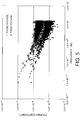
- Fig. 5 shows the frequency characteristics with respect to the fluctuations of those drain currents.
- the same random noise generating element 10a was used in those experiments.
- the gate length L was 0.12 ⁇ m, and the channel width W was 0.15 ⁇ m.
- the atom number ratio between Si and N in the trap insulating film 14 formed with a nonstoichiometric SiN film was 1:1.
- the tunnel insulating film 13 was a SiO 2 film, and has a film thickness T of 0.7 nm.
- the atom number ratio between Si and N in the SiN film 14 was almost the optimum ratio, and the material of the tunnel insulating film 13 was almost the optimum material.
- the cycle of the pulse voltage applied to the gate electrode 16 of the random noise generating element 10a was 32 ms.
- the data acquisition cycle was the same as the cycle of the applied pulse voltage.
- the film thickness T of the tunnel insulating film 13 was 0.7 nm
- the film thickness T SiN of the trap insulating film 14 formed with a silicon nitride film was 5 nm
- the film thickness T top of the control insulating film 15 was 6 nm
- the amplitude ⁇ V of the pulse voltage applied to the gate electrode 16 was 4 V.
- the electric field in the element should preferably have a size of 10 MV/cm or smaller, so as to avoid degradation of the element. Accordingly, the upper limit of the amplitude of the pulse voltage should be set with the above fact taken into consideration.
- EOT equivalent oxide thickness
- the film thickness of each insulating film is represented by an equivalent oxide thickness (EOT; for example, the EOT of a substance A (EOT(A)) is expressed as: Tphys. x( ⁇ (SiO 2 )/ ⁇ (A)) (here, Tphys.
- the value obtained by dividing the applied voltage (the amplitude of the pulse voltage) by the total film thickness determined from the equivalent oxide thicknesses of the tunnel insulating film 13, the trap insulating film 14, the control insulating film 15, and the gate electrode 16 represents the electric field induced in the random noise generating element 10a. Accordingly, the upper limit of the amplitude of the pulse voltage can be determined from the upper limit of the electric field and the film thickness of each film of the element.
- the cycle of the pulse voltage is in synchronization with the random number generating rate, and 1 Hz should be sufficient as the cycle of the pulse voltage, unless a very high generating rate is required.
- the frequency of a clock that is generally considered to be the fastest is approximately 1 GHz. Accordingly, the upper limit of the frequency of the pulse voltage to be actually applied is 1 GHz.
- the voltage to be applied to the gate electrode was adjusted so that the value of each drain current Id became approximately 2 ⁇ A. Since the random noise generating element 10a used in the experiments was an n-type MOSFET, the pulse voltage to be applied to the gate electrode was adjusted to be a positive voltage.
- the fluctuation components of the current in the random noise generating element 10a when a pulse voltage was applied were large, and to be more specific, were approximately 20% for average current.
- the fluctuation components of the current in the random noise generating element 10a when a fixed voltage was applied were small, and to be more specific, were approximately 10% for average current.
- the fluctuation components of the current in the case where a pulse voltage was applied to the gate electrode of the random noise generating element were much larger than in the case where a fixed voltage was applied to the gate electrode.
- the current fluctuation components in the case where a pulse voltage was applied were substantially larger at any frequency than in the case where a fixed voltage was applied.
- true random numbers generated with the noise obtained by applying a pulse voltage to the gate electrode 16 have higher quality than true random numbers generated with the noise obtained by applying a fixed voltage to the gate electrode 16.
- the tunnel insulating film 13 of the random noise generating element 10a is very thin. For example, in a random noise generating element having 0.1% or more of 1-MHz fluctuation components, charges move between the channel 12c and the trap insulating film 14 in a shorter mean tunneling time than 1 ⁇ s. Accordingly, if the cycle of the pulse voltage to be applied is 1 ⁇ s or longer, larger noise components than in a case where a fixed voltage is applied can be obtained at any frequency, regardless of the cycle of the pulse voltage to be applied to the gate electrode 16.
- the synchronous noise increasing effect achieved by applying a pulse voltage to the gate electrode 16 of the random noise generating element 10a is an effect discovered for the first time by the inventors conducting the experiments.
- the pulse voltage used in those experiments was a rectangular wave, the same results can be obtained with another waveform such as a sine wave or a triangular wave.
- Fig. 1 shows a random number generating device in accordance with a first embodiment of the present invention.
- the random number generating device of this embodiment includes a random noise source 10 having a random noise generating element 10a and a load resistor 10b connected in series to each other, a buffer circuit 20, a comparator 30, a buffer circuit 40, a timing circuit 50, a latch circuit 60 formed with a D-flip-flop, and a pulse voltage generator 70.
- a random noise generating element that has 0.1% or more of 1-MHz fluctuation components obtained by applying a fixed voltage is used, and the fluctuation components are increased by applying a pulse voltage to the element. Also, a random noise generating element that has 1% or more, or 0.01% or more of 1-MHz fluctuation components is also described.
- the random noise generating element 10a of the random number generating device of this embodiment is the SiN MOSFET shown in Fig. 2 .
- a silicon oxide film is used as the tunnel insulating film 13.
- the trap insulating film 14 contains traps formed with dangling bonds.
- M represents an element other than Si, O, and N.
- Fig. 6 shows the fluctuation characteristics of the drain current I d observed when a fixed voltage is applied to the gate electrode 16 of the random noise generating element 10a.
- the random noise generating element 10a used here has a gate length L of 0.06 ⁇ m, and a gate width W of 0.15 ⁇ m.
- the film thickness T of the tunnel insulating film 13 is 0.7 nm, and the ratio Si/N between the Si atom number and the N atom number in the trap insulating film 14 is 1.
- the drain current I d has a mean value of 1.00 x 10 -5 A. With the mean value being the center point, fluctuations are caused, and the half amplitude (the current fluctuation width) is 15% of the mean value at a maximum.
- Fig. 7 shows the frequency characteristics obtained by sampling the drain current waveform shown in Fig. 6 every 60 ⁇ sec and carrying out Fourier transforms.
- the data obtained through Fourier transforms are indicated by black triangular dots.
- the drain current fluctuations are formed with overlaps of frequency components.
- the amount of fluctuation components becomes smaller.
- the current fluctuation width of the current waveform shown in Fig. 6 is 15% of the mean value. If the main components of the 15% fluctuation are considered to be low-frequency components, and the 15% fluctuation components are equivalent to the 10-Hz components, the 10-Hz fluctuation components (the absolute value of the Fourier coefficient) is 8.4 x 10 -5 .
- the frequency at which 0.1% of fluctuation components is observed, or the frequency at which the absolute value of the Fourier coefficient is 8.4 x 10 -8 , is approximately 2.8 MHz according to the regression analysis equation that is set on the assumption that the frequency characteristics shown in Fig. 7 are represented by the straight line g 1 in the frequency region of 100 Hz and higher.
- the current fluctuation components at 1 MHz according to the straight line g 1 are approximately 9.0 x 10 -7 , which is 0.16% of the mean value of the drain current I d . Accordingly, the requirement that the random noise generated from the random noise generating element 10a contains 0.1% or more 1-MHz fluctuation components is satisfied.
- the structure parameters include the gate length L, the channel width W, the film thickness T of the tunnel insulating film 13, the ratio U between the Si atom number and the N atom number in the silicon nitride (Si U N, U > 0.75) serving as the trap insulating film 14.
- the abscissa axis indicates the inverse L of the gate length L
- the ordinate axis indicates the absolute value of the Fourier coefficient.
- the channel width (the gate width) W was 0.15 ⁇ m
- the film thickness T of the tunnel insulating film 13 was 0.7 nm
- the atom number ratio Si/N between Si and N in the trap insulating film 14 was 1.
- the current fluctuation components of random noise are proportional to the inverse 1/L of the gate length L.
- the Fourier coefficient was the value obtained at a frequency of 100 Hz.
- the inventors confirmed the fact that the characteristics of the current fluctuation components of random noise being proportional to 1/L did not depend on the frequency.
- the abscissa axis indicates the inverse 1/W of the channel width W
- the ordinate axis indicates the absolute value of the Fourier coefficient.
- the channel length L was 0.06 ⁇ m
- the film thickness T of the tunnel insulating film 13 was 0.7 nm
- the atom number ratio Si/N between Si and N in the trap insulating film 14 was 1. The graph shown in Fig.
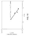
- the dependence of the absolute value of the Fourier coefficient on the film thickness T of the tunnel insulating film 13 at a frequency of 250 Hz was examined, and the result is shown in Fig. 10 .
- the abscissa axis indicates the film thickness T of the tunnel insulating film 13
- the ordinate axis indicates the absolute value of the Fourier coefficient.
- the channel length L was 0.06 ⁇ m
- the channel width W was 0.15 ⁇ m
- the atom number ratio Si/N between Si and N in the trap insulating film 14 was 1.
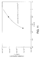
- Fig. 11 the abscissa axis indicates the atom number ratio U between the Si atoms and the N atoms in the trap insulating film 14, and the ordinate axis indicates the absolute value of the Fourier coefficient.
- the channel length L was 0.06 ⁇ m
- the channel width W was 0.15 ⁇ m
- the film thickness T of the tunnel insulating film 13 was 0.07 nm.
- This theoretical model was formed based on the concept that fluctuations were proportional to (the number of overlaps (trap density)) 1/2 according to the central limiting theorem of statistics.
- a x 0.0117411 ⁇ 2 observed when U is 0.75 is a guide of the noise intensity that can be obtained stoichiometrically.
- the Fourier coefficient was the value obtained at the frequency of 300 Hz.
- the experiment data shown in Figs. 3 to 11 are the results the inventors obtained through experiments.
- the conditions for the current fluctuation components (Fourier coefficient) of the drain current to have 1-MHz fluctuation components at a rate of 0.1% or higher with the respective parameters are described.
- the trap insulating film 14 of the random noise generating element 10a used in the above experiments was a Si nitride film containing excess Si. However, it is considered that the same behaviors as above can be observed in a random noise generating element that has a Si-rich oxynitride film (Si x (SiO 2 ) y (Si 3 N 4 ) 1-y , x > 0, 1 ⁇ y ⁇ 0).
- a Si-rich nitride film has a stoichiometric composition of Si 3 N 4 . Therefore, the number of Si dangling bonds per atom in Si U N is (U-0.75)/(U+1), and is 0.125 where Si/N is 1 and U is 1. Meanwhile, a Si-rich oxynitride film (Si x (SiO 2 ) y (Si 3 N 4 ) 1-y , x > 0, 1 ⁇ y ⁇ 0) becomes stoichiometric where x is 0.
- the number of excess Si atoms per atom is x/(x+7-4y), and dangling bonds are formed when one excess Si atom having four atomic bonding hands is replaced with an N atom having three atomic bonding hands and an O atom having two atomic bonding hands.
- the probability that an excess silicon atom is replaced with N and O atoms is determined by the atom number ratio between N and O.
- One dangling bond is formed when one excess Si atom is replaced with one N atom having three atomic bonding hands.
- Two dangling bonds are formed when one excess Si atom is replaced with O atoms having two atomic bonding hands.
- the number of dangling bonds per atom is x/(x+7-4y) x [(4-4y)/(4-2y)+ ⁇ 2y/(4-2y) ⁇ x2].
- x is 15/29, where y is 0.5.
- the frequency of the clock to be used should preferably be lower in the neighborhood of 100 MHz.
- the fluctuation components in the 1- ⁇ s cycle are 10 ns (the inverse of the clock frequency of 100 MHz) or more, which is 1%.
- a random noise generating element that can generate random numbers containing 1-MHz fluctuation components at 1% or more is obtained, if the following equation (4) is satisfied: [ x / x + 7 - 4 ⁇ y ⁇ 4 - 4 ⁇ y / 4 - 2 ⁇ y + 2 ⁇ y / 4 - 2 ⁇ y ⁇ 2 + 0.01174 ⁇ ] 1 / 2 ⁇ exp - T ⁇ H / 3.1 ⁇ ⁇ 1 /
- the random generating rate does not need to be so high. In such cases, this embodiment can also be used.
- the gate length L [ ⁇ m], the channel width (gate width) W [ ⁇ m], the film thickness T [nm] of the tunnel insulating film, and the atom number ratios x and y (x > 00 ⁇ y ⁇ 1) have arbitrary values
- a random noise generating element that can generate random numbers containing 1-MHz oscillation components at 0.01% or more is obtained, if the following equation (6) is satisfied: [ x / x + 7 - 4 ⁇ y ⁇ 4 - 4 ⁇ y / 4 - 2 ⁇ y + 2 ⁇ y / 4 - 2 ⁇ y ⁇ 2 + 0.01174 ⁇ ] 1 / 2 ⁇ exp - T ⁇ H / 3.1
- the random noise generated by applying a pulse voltage can achieve the above value.
- the following is a description of the effect of application of a pulse voltage to the gate electrode 16 of a random noise generating element 10a, and the conditions for the random noise generated from the random noise generating element 10a to have 1-MHz fluctuation components at 0.01% or more, 0.1% or more, or 1% or more.
- the random noise obtained when a pulse voltage is applied to the gate electrode 16 of a random noise generating element 10a is three times as large as the random noise obtained when the gate voltage is fixed, as can be seen from Fig. 5 showing the frequency characteristics of the fluctuations of the drain current I d .
- the straight line g 2 in Fig. 7 is obtained by regression analysis carried out on the size of the random noise obtained when a pulse voltage is applied to the gate electrode 16 of the random noise generating element 10a as in this embodiment, or the size of the absolute value of the Fourier coefficient.
- the gate length L was 0.06 ⁇ m
- the gate width W was 0.15 ⁇ m
- the film thickness T of the tunnel insulating film 13 was 0.7 nm
- the atom number ratio Si/N in the trap insulating film 14 formed with a silicon nitride film was 1.
- the drain current fluctuations when a fixed voltage is applied to the gate electrode have 15% current fluctuation components in the neighborhood of 10 ⁇ A.
- the current fluctuation components at 1 MHz are approximately 0.16%. Accordingly, the requirement that the fluctuation components at 1 MHz should be 0.1% or more is satisfied.
- the current fluctuation components observed at 1 MHz are approximately 0.48%. Accordingly, the requirement that the fluctuation components at 1 MHz should be 0.1% or more is satisfied. It is also considered that the effect of a pulse voltage applied to the gate electrode does not have the frequency dependence, since a very thin tunnel insulating film is employed.
- random noise generating elements 10a having different structure parameters were produced.
- the characteristics observed in a case where a pulse voltage was applied to the gate electrode 16 of each of those random noise generating elements 10a, and the characteristics observed in a case where a fixed voltage was applied to the gate electrodes 16 were examined.
- the structure parameters include the gate length L, the channel width (gate width) W, and the film thickness T of the tunnel insulating film.
- the cycle of the pulse voltage was 32 ms, and ⁇ V was 4 V.
- the film thickness T SiN of the trap insulating film 14 was 5 nm
- the film thickness T top of the control insulating film 15 was 6 nm. Those values are not varied even if the channel length L, the channel width W, and the film thickness T of the tunnel insulating film are varied.
- the channel width W was 0.15 ⁇ m
- the film thickness T of the tunnel insulating film 13 was 0.7 nm
- the atom number ratio Si/N between Si and N in the trap insulating film 14 was 1.
- the Fourier coefficient shown in Fig. 12 was measured at a frequency of 5 Hz.
- the size of the random noise was substantially proportional to the inverse L of the channel length L in both cases where a pulse voltage was applied and where a fixed voltage was applied.
- the random noise obtained when a pulse voltage was applied to the gate electrode was three times as large as the random noise obtained when a fixed voltage was applied to the gate electrode.
- the random noise obtained when a pulse voltage was applied was random noise in synchronization with the pulse voltage.
- the channel length L was 0.12 ⁇ m
- the film thickness T of the tunnel insulating film 13 was 0.7 nm
- the atom number ratio Si/N between Si and N in the trap insulating film 14 was 1.
- the Fourier coefficient shown in Fig. 13 was measured at a frequency of 1.5 Hz.
- the size of the random noise was proportional to the square of the inverse 1/W of the channel width W in both cases where a pulse voltage was applied and where a fixed voltage was applied.
- the random noise obtained when a pulse voltage was applied to the gate electrode was three times as large as the random noise obtained when a fixed voltage was applied to the gate electrode.
- the shown random noise obtained when a pulse voltage was applied was random noise in synchronization with the pulse voltage.
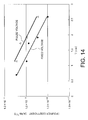
- Fig. 14 the dependence of the Fourier coefficient on the film thickness T of the tunnel insulating film was examined, and the result is shown in Fig. 14 .
- the channel length L was 0.06 ⁇ m
- the channel width W was 0.15 ⁇ m
- the atom number ratio Si/N between Si and N in the trap insulating film 14 was 1.
- the Fourier coefficient shown in Fig. 14 was measured at a frequency of 1.1 Hz.
- the size of the random noise became smaller exponentially with respect to the film thickness T of the tunnel insulating film 13 in both cases where a pulse voltage was applied and where a fixed voltage was applied.
- C [ x / x + 7 - 4 ⁇ y + z ⁇ 4 - 4 ⁇ y / 4 - 2 ⁇ y + 2 ⁇ y / 4 - 2 ⁇ y ⁇ 2 + 0.01174 ⁇ ] 1 / 2 ⁇ exp - T ⁇ H / 3.1 ⁇ ⁇ 1 / 2 / 0.8664 / LW 2 / 5
- the Fourier coefficient of random noise is proportional to the product C.
- T represents the film thickness [nm] of the tunnel insulating film
- H represents the barrier height [eV] between the semiconductor substrate and the tunnel insulating film.
- the product C is 5.8678 [ ⁇ m -7/5 ], when the gate length L is 0.06 ⁇ m, the cannel width (gate width) W is 0.15 ⁇ m, the film thickness T of the tunnel insulating film is 0.7 nm, and the atom number ratio between the Si atoms and the N atoms in the trap insulating film is 1.
- the proportion of the current fluctuations at 1 MHz is 0.16%.
- the current fluctuations can be made three times as large as those of the other case, and the proportion of the current fluctuations at 1 MHz is 0.48% accordingly.
- the proportion of the current fluctuation components at 1 MHz is 0.1% or larger, if the product C of the characteristics with respect to the respective parameters is larger than 5.87 x (0.1/0.16).
- the proportion of the current fluctuation components at 1 MHz can be 0.1% or larger, if the product C of the characteristics with respect to the respective parameters is larger than 5.87 x (0.1/0.48).
- the conditional equation about the product C of the characteristics with respect to the parameters used in the case where a fixed voltage is applied can also be used in this embodiment by multiplying the right-hand side of the equation by 1/3.
- the required amount of current fluctuation components varies with the experiment conditions.
- the above equation is used where the proportion of the current fluctuation components is 0.1% or more. In cases where the proportion of the current fluctuation components is 0.01% or larger and where the proportion of the current fluctuation components is 1% or larger, the right-hand side of the above conditional equation used when a fixed voltage is applied should be multiplied by 1/3.
- the value of LW can be made larger than the value of LW obtained in the case where a fixed voltage is applied. Accordingly, in accordance with the present invention, a higher degree of freedom is allowed in the design of a random noise generating element, and there is no need to employ a difficult miniaturization technique.
- the trap insulating film 14 is expressed as Si x (SiO 2 ) y (Si 3 N 4 ) 1-y M z (x > 0, 1 ⁇ y ⁇ 0, z ⁇ 0), where M represents an element other than Si, O, and N.
- M represents an element other than Si, O, and N.
- the conditions for the proportion of the 1-MHz fluctuation components of random noise to be 0.01% or larger, 0.1% or larger, and 1% or larger in the case where the trap insulating film 14 of a random noise generating element 10a is Si U N (U ⁇ 0.75) are as follows.
- the trap insulating film 14 is formed with a stoichiometric silicon oxynitride film or a nonstoichiometric silicon oxynitride film in the above described embodiment.
- the trap insulating film 14 is formed only with a nonstoichiometric silicon oxynitride film expressed by the composition formula Si x (SiO 2 ) y (Si 3 N 4 ) 1-y M 2 (x ⁇ 0, 1 ⁇ y ⁇ 0, z ⁇ 0)
- the following equations (17), (18), and (19) having the stoichiometric term 0.01174 removed from the equations (12), (11), and (13) are to be satisfied.
- a random noise signal (a voltage signal that has the same cycle as the pulse voltage 75 and exhibits amplitude having a random level) is generated from the connection node between the random noise generating element 10a and the resistor 10b.
- This random noise signal is input to the buffer circuit 20.
- An output signal from the buffer circuit 20 is input to one terminal of the comparator 30.
- the reason that the buffer circuit 20 is provided is as follows. If the random noise generating element 10a is connected directly to the comparator 30, proper random noise might not be obtained due to adverse influence of the comparator 30. Therefore, to shut off the influence of the comparator 30, the buffer circuit 20 is provided. Also, a voltage signal that is a reference voltage V ref is supplied to the other terminal of the comparator 30.
- the comparator 30 performs a comparison between two signals that are input to the comparator 30, and outputs a high-level signal or a low-level signal.
- the value of the reference voltage V ref is set at a value substantially equal to the mean value of signals that are output from the buffer circuit 20. With this arrangement, the random signals that are output from the comparator 30 have the value "1" and "0" at the same rates. However, the output level of the comparator 30 might become insufficient, depending on the size of the signal that is input to the comparator 30 or the rate of change of input signals.
- the buffer circuit 40 is provided on the output side of the comparator 30 in this embodiment. The buffer circuit 40 amplifies the output of the comparator 30, to obtain a desired voltage level.
- the output signal from the buffer circuit 40 is input to the latch circuit 60 formed with a D-flip-flop, and is latched with an appropriate clock signal, so as to generate a random number.
- the clock signal that is input to the latch circuit 60 here may be acquired from the pulse voltage generator 70 that generates the pulse voltage to be applied to the gate electrode 16 of the random noise generating element 10a.
- the clock 75 is input to the clock terminal of the latch circuit 60 via the timing circuit 50 formed with an inverter or the like.
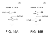
- the buffer circuit 20 may have circuit structures shown in Figs. 15A and 15B , for example.
- the buffer circuit 20 is formed with a p-type MOSFET 21 and a resistor 22 that are connected in series.
- the buffer circuit 20 is formed with an n-type MOSFET 23 and a resistor 24 that are connected in series.
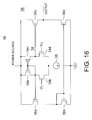
- Fig. 16 illustrates a specific example of the comparator 30.
- the comparator 30 of this example includes a differential amplifier 34, a current source 35, and an output unit 36.
- the differential amplifier 34 includes a p-type MOSFET 34a and an n-type MOSFET 34b that are connected in series, and a p-type MOSFET 34c and an n-type MOSFET 34d that are connected in series.
- the output unit 36 includes a p-type MOSFET 36a and an n-type MOSFET 36b that are connected in series, and a p-type MOSFET 36c and an n-type MOSFET 36d that are connected in series.
- the drains of the p-types MOSFETs 34a, 34c, 36a, and 36c are connected to the power source.
- the gate of the p-type MOSFET 36a is connected to the connection node between the p-type MOSFET 34a and the n-type MOSFET 34b.
- the gate of the p-type MOSFET 36c is connected to the connection node between the p-type MOSFET 34c and the n-type MOSFET 34d.
- the sources of the n-type MOSFETs 34b and 34d are connected to each other and are grounded via the current source 35.
- the n-type MOSFETs 36b and 36d have the respective gates connected to the common connection node of the p-type MOSFET 36a and the n-type MOSFET 36b, and have the respective drains grounded.
- a first input voltage V i1 is input to the gate of the n-type MOSFET 34b of the differential amplifier 34, and a second input voltage V i2 is input to the gate of the n-type MOSFET 34d.
- An output voltage is output from the common connection node of the p-type MOSFET 36c and the n-type MOSFET 36d. If the first input voltage V i1 is higher than the second input voltage V i2 , the output voltage is a low-level voltage.
- the output voltage is a high-level voltage.
- the buffer circuit 40 is connected to the output stage of the comparator 30.
- Fig. 17 shows a specific example structure of the buffer circuit 40.
- the buffer circuit 40 of this specific example is an inverter circuit that includes a p-type MOSFET 42 and an n-type MOSFET 44.
- the buffer circuit 40 amplifies the output of the comparator 30, so as to obtain a digital signal having a sufficient voltage level.
- the random number generating device of this embodiment has the random noise generating element 10a in which a pulse voltage is applied to the gate electrode 16 as shown in Fig. 2 . Accordingly, it is possible to generate random numbers at a high speed.
- the number of inverters employed in the buffer circuit 40 is adjusted so that an optimum random number generating device capable of coping with the proportion of the fluctuation components at 1 MHz can be obtained.
- the voltage to be applied to the gate electrode 16 of the random noise generating element 10a depends on the silicon bandgap. Accordingly, if the fluctuations of the voltage that is output from the random noise generating element 10a, that is, the fluctuations of the voltage that is output from the connection node between the random noise generating element 10a and the resistor 10b which correspond the fluctuations of the current of the random noise generating element 10a are of 10 mV, the proportion of the fluctuation components is approximately 1% of the input voltage. Likewise, if the fluctuations of the voltage that is output from the random noise generating element 10a are of 1 mV, the proportion of the fluctuation components is approximately 0.1% of the input voltage.
- the proportion of the fluctuation components is approximately 0.01% of the input voltage.
- the gain of the operation amplifier forming the comparator 30 is typically 100 at 1 MHz. Accordingly, if the voltage fluctuation is of 10mV or so, digital random number signals can be acquired without the use of the buffer circuit 40. If the voltage fluctuations are of 0.1 mV, one inverter is provided as the buffer circuit 40, so as to obtain digital random number signals. If the voltage fluctuations are of 0.01 mV, two inverters connected in series are provided as the buffer, so as to obtain digital random number signals. The above described facts were also confirmed through circuit simulations.
- the output of the comparator 30 is amplified by two inverters, so as to form a small-sized, high-speed random number generating device.
- the buffer circuit 40 can be formed with one inverter. With a random noise generating element 10a that can generate random noise having 1% or more fluctuation components at 1 MHz, a small-sized, high-speed random number generating device can be formed without the buffer circuit 40.
- this embodiment can provide a high-performance random number generating device that is capable of generating high-quality random numbers at a high speed.
- Fig. 18 illustrates a random number generating device in accordance with a second embodiment of the present invention.
- the random number generating device of this embodiment differs from the random number generating device of the first embodiment shown in Fig. 1 in that a delay circuit 80 to receive the output of the buffer circuit 20 is newly added, and the output of the delay circuit 80 is used as the reference voltage Vref in the comparator 30.
- the random noise generating element 10a has the same structure as that of the first embodiment, and the pulse voltage 75 generated from the pulse voltage generator 70 is applied to the gate of the random noise generating element 10a.
- a random noise signal (a voltage signal that has the same cycle as the pulse voltage 75 and exhibits amplitude having a random level) that is output from the random noise generating element 10a when the pulse voltage 75 is applied to the gate electrode is sent to the buffer circuit 20.
- the output of the buffer circuit 20 is sent to one of the input terminals of the comparator 30, and is also sent to the delay circuit 80.
- the delay circuit 80 delays the output of the buffer circuit 20 by the amount equivalent to one cycle or an integral multiple of the cycle, and outputs the delayed signal to the other input terminal of the comparator 30.
- the comparator 30 performs a comparison between the two signals that are input to the comparator 30, and outputs a high-level signal or a low-level signal.
- the two signals to be compared are signals that are output from the same random number source. If the random numbers are at random, the digital random numbers that are output from the comparator 30 include the value "1" and the value "0" randomly, and the probabilities of occurrence of "1" and "0" become equal to each other. However, depending on the size of each signal that is input to the comparator 30, and on the rate of change of the input signals, the output level of the comparator 30 might be insufficient. To counter this problem, the buffer circuit 40 is connected to the comparator 30, as in the first embodiment.
- the buffer circuit 40 amplifies the output of the comparator 30, so as to achieve a desired voltage level.
- the output signal from the buffer circuit 40 is input to the latch circuit 60 formed with a D-flip-flop, for example.
- the latch circuit 60 latches the signal with an appropriate clock, and generates a random number.
- the clock signal that is input to the latch circuit 60 here may be acquired from the pulse voltage source (the pulse voltage generator 70) of the pulse voltage applied to the gate electrode of the random noise generating element 10a of the random noise source 10.
- the clock signal is input to the clock terminal of the latch circuit 60 via the timing circuit 50 formed with an inverter or the like.
- the random noise generating element 10a of the first embodiment is used as the random noise generating element in the random number generating device of this embodiment. Accordingly, the random number generating device of this embodiment can generate high-quality random numbers at a high speed.
- the number of inverters to be employed in the buffer circuit 40 is adjusted so as to generate optimum random numbers in accordance with the proportion of the fluctuation components obtained at 1 MHz in the random number generating device of this embodiment.
- the reference voltage Vref that is required in the first embodiment as shown in Fig. 1 is not necessary.
- the reference voltage Vref needs to be set in the neighborhood of the mean voltage of the outputs of the buffer circuit 20, but such arrangement is not necessary in this embodiment.
- Fig. 19 illustrates a random number generating device in accordance with a third embodiment of the present invention.
- the random number generating device of this embodiment includes an astable multivibrator 101 and a counter 110.
- the astable multivibrator 101 includes a capacitor 102a, a NAND circuit 103a, a diode 104a, a feedback resistor 105a, a capacitor 102b, a NAND circuit 103b, a diode 104b, and a random noise generating element 10a.
- One end of the capacitor 102a is connected to the two input terminals of the NAND circuit 103a and the input terminal of the diode 104a.
- the output terminal of the diode 104a is connected to one end of the feedback resistor 105a.
- the other end of the feedback resistor 105a and the output end of the NAND circuit 103a are connected to each other, and are connected to one end of the capacitor 102b.
- the other end of the capacitor 102b is connected to one input terminal of the NAND circuit 103b and the input terminal of the diode 104b.
- An ON/OFF signal from the outside is input to the other input terminal of the NAND circuit 103b.
- One of the source and drain of the random noise generating element 10a is connected to the output end of the diode 104b.
- the other one of the source and drain of the random noise generating element 10a and the output end of the NAND circuit 103b are connected to each other, and are connected to the other end of the capacitor 102a.
- this astable multivibrator 101 one of the feedback resistors normally provided in a multivibrator, or the feedback resistor connected between the output terminal of the diode 104b and the output terminal of the NAND circuit 103b, is replaced with the random noise generating element 10a.
- the output of the multivibrator 101 (the output of the NAND circuit 103a) is applied to the gate of the random noise generating element 10a.
- the counter 110 includes a clock enable terminal and a CK terminal. Each random oscillation signal that is output from the multivibrator 101 is input to the clock enable terminal of the counter 110, and a clock generated from a ring oscillator or the like is input to the CK terminal. With this arrangement, the random oscillation signals are counted, and "1" or "0" is output by determining whether the count value is an odd number or an even number.
- the multivibrator 101 including the random noise generating element 10a is oscillated at 1 MHz.
- the fluctuation width of the oscillation cycle of the signals that are output from the multivibrator 101 is counted with a 1-GHz clock with the use of a ring oscillator.
- the count values can be turned into digital random numbers from the noise components generated from the random noise generating element 10a, with the use of a 1-GHz clock that is normally considered to be the fastest.
- true random numbers can be generated at a random number generating rate of 1 MHz/sec or higher, without an amplifier circuit.
- the circuit size can be made smaller than in the first and second embodiments.
- the random noise generating element 10a of the first embodiment is used as the random noise generating element in the random number generating device of each of the second and third embodiments. Accordingly, the random number generating device of each of the second and third embodiments can generate high-quality random numbers at a high speed.
- the conditions for the proportion of the 1-MHz fluctuation components in the random noise generated from the random noise generating element 10a to be 0.01% or higher, 0.1% or higher, and 1% of higher are the same as those described in the first embodiment.
- Random noise generating elements 10a that can be used in the first to third embodiments are not limited to those described above.
- the same effects as above can be achieved with a random noise generating element that does not include a tunnel insulating film and has a SiN film placed directly on the substrate (a regular MOSFET having a gate insulating film formed with a SiN film), or a random noise generating element that has a tunnel insulating film formed with a material that is other than SiO 2 and has a smaller barrier height.
- the same effects above can also be achieved with a random noise generating element that does not have the control insulating film 15. Further, it is also possible to achieve the same effects as above, even if the control insulating film 15 is thin.
- Fig. 20 illustrates a random number generating device in accordance with a fourth embodiment of the present invention.
- the random number generating device of this embodiment is the same as the random number generating device of the first embodiment shown in Fig. 1 , except that the random noise source 10 is replaced with a random noise source 10A.
- the random noise source 10A has a random noise generating element 10c, instead of the random noise generating element 10a.
- the random noise generating element 10c is a MOSFET.
- a source region 12a and a drain region 12b are formed on the surface region of a silicon substrate (a semiconductor substrate) 11.
- the region of the semiconductor substrate located between the source region 12a and the drain region 12b serves as the channel region 12c. It is preferable that the gate length L and the channel width (the gate width) W of the channel region 12c are small.
- the channel region 12c may be a region having a thin portion as part of the channel, with the thin portion having the length L and the width W.
- the source region 12a and the drain region 12b contain n-type impurities such as phosphorus (P) and arsenic (As).
- the channel region 12c, the source region 12a, and the drain region 12b are isolated from one another by device isolating insulating regions (not shown).
- a tunnel insulating film 13a formed with a nitride film is provided on the channel region 12c, and conductive fine particles 17 containing Si, for example, are provided on the tunnel insulating film 13a.
- a control oxide film (a control insulating film) 15 is formed to cover the fine particles 17.
- the random noise generating element 10c is produced in the following manner.
- the surface of the semiconductor substrate 11 is nitrided through thermal nitridation using NH 3 , so as to form the tunnel insulating film 13a that is a nitride film having a thickness T of 0.8 nm.
- the fine particles 17 that are Si microcrystals having a mean particle size of 8 nm are formed on the tunnel insulating film 13a with a surface density of approximately 1.7 x 10 12 cm -2 .
- the particle size of the fine particles 17 is controlled by adjusting the CVD time, and the surface density can be controlled by adjusting the temperature, the raw material gas flow rate and the number of CVD times.
- the control insulating film 15 made of SiO 2 is formed to cover the fine particles 17 by CVD, and the gate electrode 16 made of polysilicon is formed on the control insulating film 15.
- the random noise generating element 10c used in this embodiment can generate larger random noise in a case where a pulse voltage is applied to the gate electrode 16 than in a case where a fixed voltage is applied to the gate electrode 16.
- the random noise generating element 10c used in this embodiment has the same structure as the random noise generating element disclosed in US 2005/0180219 A1 . More specifically, as disclosed in US 2005/0180219 A1 , the random noise generating element 10c used in this embodiment has a semiconductor channel that include a thin portion having a width W and a length L, with W ⁇ ( ⁇ /10( ⁇ m 2 ))/L being satisfied.
- a tunnel insulating film is provided on the semiconductor channel, and conducive fine particles that can charge or discharge electrons to and from the semiconductor channel via the tunnel insulating film are provided above the semiconductor channel via the tunnel insulating film, with a surface density of 2.5 x 10 11 cm -2 or higher.
- the conditions for obtaining 0.1% or more of fluctuation components at 1 MHz can be expressed as: D dot ⁇ d 3 / 4 / W ⁇ exp - 8 ⁇ ⁇ T ( 2 ⁇ mH ⁇ ) 1 / 2 / 3 ⁇ h ⁇ ( 0.5 / L ⁇ ) 1 / 2 ⁇ 4 ⁇ ⁇ m - 5 / 3
- D dot represents the surface density of the conductive fine particles
- d represents the mean particle size
- W represents the width of the thin portion
- T represents the thickness of the tunnel insulating film
- H represents the energy barrier height between the semiconductor substrate and the tunnel insulating film
- h represents the Planck's constant
- q represents the elementary charge
- m represents the effective mass tunneling the tunnel insulating film
- ⁇ represents the dielectric constant of the tunnel insulating film.
- the conductive fine particles it is preferable to use silicon crystalline fine particles, and more preferable to use metal fine particles of Au, Ag, or Al etc.
- the tunnel insulating film 13a of the random noise generating element 10c used in this embodiment is very thin, and it is considered that charges are moving between the channel and the trap at a high speed.
- charges can have a larger amount of noise components at any frequency when a pulse voltage is applied as in this embodiment, than in a case where the voltage to be applied to the gate electrode 16 is fixed.
- the random number generating device of this embodiment can generate high-quality random numbers at a high speed. Also, as in US 2005/0180219 A1 , it is not necessary to employ an amplifier circuit. Thus, a small-sized random number generating device can be obtained.
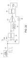
- Fig. 22 illustrates a random number generating device in accordance with a fifth embodiment of the present invention.
- the random number generating device of this embodiment is the same as the random number generating device of the second embodiment shown in Fig. 18 , except that the random noise generating element 10a is replaced with the random noise generating element 10c shown in Fig. 21 .
- high-quality random numbers can be generated at a high speed, as in the second embodiment and the fourth embodiment.
- Fig. 23 illustrates a random number generating device in accordance with a sixth embodiment of the present invention.
- the random number generating device of this embodiment is the same as the random number generating device of the third embodiment shown in Fig. 19 , except that the random noise generating element 10a is replaced with the random noise generating element 10c shown in Fig. 21 .
- high-quality random numbers can also be generated at a high speed, as in the third embodiment and the fourth embodiment.
- the tunnel insulating film 13 is formed through thermal oxidation.
- a natural oxide film that is formed in the atmosphere is also possible.
- a silicon substrate is used as the semiconductor substrate.
- a semiconductor substrate made of a material other than silicon is used as the semiconductor substrate.
- the input pulse frequency is equal to the random number generating rate.
- the ratio of the input pulse frequency to the random number generating rate may be an integer.
- the delay in the delay circuit 90 may be adjusted so that the (input pulse frequency/generating rate) becomes a rational number.
- Synchronous random noise reinforcement by a pulse input leads to random noise reinforcement in the periodic components of the pulse. Accordingly, in a case where random noise is converted into clock digital signals through oscillation outputs as in the third embodiment, random noise reinforcement by a pulse can be used, even if the (input pulse/generating rate) is a surd.
- a random noise generating device in accordance with the present invention is not limited to any of the random number generating devices of the first to sixth embodiments, as long as it includes a circuit that can achieve a noise increasing effect by applying a pulse voltage to the gate electrode.
Landscapes
- Physics & Mathematics (AREA)
- General Physics & Mathematics (AREA)
- Engineering & Computer Science (AREA)
- Theoretical Computer Science (AREA)
- Computational Mathematics (AREA)
- Mathematical Analysis (AREA)
- Mathematical Optimization (AREA)
- Pure & Applied Mathematics (AREA)
- General Engineering & Computer Science (AREA)
- Insulated Gate Type Field-Effect Transistor (AREA)
Applications Claiming Priority (1)
| Application Number | Priority Date | Filing Date | Title |
|---|---|---|---|
| JP2007145095A JP4365872B2 (ja) | 2007-05-31 | 2007-05-31 | 乱数生成装置 |
Publications (1)
| Publication Number | Publication Date |
|---|---|
| EP2000903A1 true EP2000903A1 (de) | 2008-12-10 |
Family
ID=39629067
Family Applications (1)
| Application Number | Title | Priority Date | Filing Date |
|---|---|---|---|
| EP08157169A Withdrawn EP2000903A1 (de) | 2007-05-31 | 2008-05-29 | Zufallszahlengenerator |
Country Status (3)
| Country | Link |
|---|---|
| US (1) | US8307022B2 (de) |
| EP (1) | EP2000903A1 (de) |
| JP (1) | JP4365872B2 (de) |
Families Citing this family (15)
| Publication number | Priority date | Publication date | Assignee | Title |
|---|---|---|---|---|
| JP4160605B2 (ja) * | 2006-05-09 | 2008-10-01 | 株式会社東芝 | 乱数発生装置 |
| US8509295B1 (en) * | 2008-09-04 | 2013-08-13 | Marvell Israel (M.I.S.L) Ltd. | Bit error rate prediction |
| JP5433686B2 (ja) | 2009-05-22 | 2014-03-05 | 株式会社東芝 | 乱数生成回路およびこれを用いた暗号回路 |
| US8522065B2 (en) * | 2009-09-06 | 2013-08-27 | Percello Ltd. | Generating a random number in an existing system on chip |
| JP6380804B2 (ja) | 2014-04-16 | 2018-08-29 | パナソニックIpマネジメント株式会社 | 乱数処理装置および乱数処理方法 |
| CA2948408C (en) | 2014-05-09 | 2023-03-07 | Quantum Numbers Corp. | Method for generating random numbers and associated random number generator |
| JP6674616B2 (ja) | 2015-06-10 | 2020-04-01 | パナソニック株式会社 | 半導体装置、半導体装置の読み出し方法、及び半導体装置を搭載したicカード |
| FR3072481B1 (fr) | 2017-10-12 | 2019-11-08 | Stmicroelectronics | Dispositif de generation d'un signal aleatoire |
| US10168996B1 (en) | 2018-01-15 | 2019-01-01 | Quantum Numbers Corp. | Method and system for generating a random bit sample |
| US10983757B2 (en) * | 2019-02-25 | 2021-04-20 | United States Of America As Represented By The Secretary Of The Navy | Nanomaterial-based true random number generator |
| CN110286878B (zh) * | 2019-06-25 | 2021-06-01 | 电子科技大学 | Mcu随机间隔转换电桥电压的真随机数产生器及产生方法 |
| CN110808728B (zh) * | 2019-11-19 | 2023-10-20 | 天津津航计算技术研究所 | 基于高速动态比较器的随机信号发生方法 |
| CN114157243B (zh) * | 2021-11-26 | 2022-11-29 | 南京鼓楼医院 | 一种基于可调异质结的白噪声发生方法 |
| US11907686B1 (en) | 2023-08-11 | 2024-02-20 | Veiovia Limited | True random number generation based on instrument data |
| KR102940673B1 (ko) * | 2024-07-19 | 2026-03-18 | 고려대학교 산학협력단 | 정보 암호화가 가능한 게이트 다이오드 기반 진성 난수 발생기 |
Citations (2)
| Publication number | Priority date | Publication date | Assignee | Title |
|---|---|---|---|---|
| US20050180219A1 (en) | 2003-12-05 | 2005-08-18 | Ryuji Ohba | Random number generating element |
| EP1855191A2 (de) * | 2006-05-09 | 2007-11-14 | Kabushiki Kaisha Toshiba | Zufallszahlengenerator |
Family Cites Families (6)
| Publication number | Priority date | Publication date | Assignee | Title |
|---|---|---|---|---|
| FR2817361B1 (fr) * | 2000-11-28 | 2003-01-24 | St Microelectronics Sa | Generateur de signal aleatoire |
| JP3604658B2 (ja) | 2001-09-26 | 2004-12-22 | 株式会社東芝 | 乱数生成回路 |
| JP4118754B2 (ja) | 2003-06-27 | 2008-07-16 | 日本電信電話株式会社 | 乱数発生回路 |
| JP3803664B2 (ja) | 2003-09-30 | 2006-08-02 | 株式会社東芝 | 乱数生成回路、半導体集積回路、icカード及び情報端末機器 |
| JP2006189946A (ja) | 2004-12-28 | 2006-07-20 | Toshiba Corp | 乱数生成回路及び半導体集積回路 |
| JP4940618B2 (ja) | 2005-10-07 | 2012-05-30 | ソニー株式会社 | 半導体装置 |
-
2007
- 2007-05-31 JP JP2007145095A patent/JP4365872B2/ja active Active
-
2008
- 2008-05-29 EP EP08157169A patent/EP2000903A1/de not_active Withdrawn
- 2008-05-30 US US12/130,567 patent/US8307022B2/en active Active
Patent Citations (2)
| Publication number | Priority date | Publication date | Assignee | Title |
|---|---|---|---|---|
| US20050180219A1 (en) | 2003-12-05 | 2005-08-18 | Ryuji Ohba | Random number generating element |
| EP1855191A2 (de) * | 2006-05-09 | 2007-11-14 | Kabushiki Kaisha Toshiba | Zufallszahlengenerator |
Non-Patent Citations (2)
| Title |
|---|
| M. MATSUMOTO ET AL.: "International Conference on Solid State Devices and Materials", SSDM (SOLID STATE DEVICE AND MATERIALS, 2006, pages 280 - 281 |
| S. YASUDA ET AL., INTERNATIONAL CONFERENCE ON SOLID STATE DEVICES AND MATERIALS, 2002, pages 250 - 251 |
Also Published As
| Publication number | Publication date |
|---|---|
| JP2008299595A (ja) | 2008-12-11 |
| US8307022B2 (en) | 2012-11-06 |
| US20090327379A1 (en) | 2009-12-31 |
| JP4365872B2 (ja) | 2009-11-18 |
Similar Documents
| Publication | Publication Date | Title |
|---|---|---|
| US8307022B2 (en) | Random number generating device | |
| US8039890B2 (en) | Random number generating device | |
| Guo et al. | A room-temperature silicon single-electron metal–oxide–semiconductor memory with nanoscale floating-gate and ultranarrow channel | |
| Fair et al. | Threshold-voltage instability in MOSFET's due to channel hot-hole emission | |
| EP2079163B1 (de) | Zufallszahlengeneratorvorrichtung | |
| US7573094B2 (en) | Random number generating element | |
| Scholten et al. | Hypothesis to explain threshold drift due to dynamic bipolar gate stress | |
| Duhan et al. | Endurance study of silicon-doped hafnium oxide (HSO) and zirconium-doped hafnium oxide (HZO)-based FeFET memory | |
| Krčmar et al. | Exact surface solutions for semiconductors: The Dember effect and partial currents | |
| Chen et al. | Interface trap generation by FN injection under dynamic oxide field stress | |
| Shah et al. | Hot carriers in semiconductors probed by picosecond techniques | |
| US4389590A (en) | System for recording waveforms using spatial dispersion | |
| Fujita et al. | Si nanodevices for random number generating circuits for cryptographic security | |
| Nedev et al. | Metal-Oxide-Semiconductor Structures Containing Silicon Nanocrystals for Application in Radiation Dosimeters | |
| Beguwala et al. | An improved model for the charging characteristics of a dual-dielectric (MNOS) nonvolatile memory device | |
| US7132878B2 (en) | Charge pump current source | |
| Lam et al. | Surface-state density and surface potential in MIS capacitors by surface photovoltage measurements. II | |
| Wu et al. | High-performance non-volatile CdS nanobelt-based floating nanodot gate memory | |
| Iye et al. | Hall mobility of hot electrons in CdS | |
| Fujieda et al. | Influence of charge traps within HfSiON bulk on positive and negative bias temperature instability of HfSiON gate stacks | |
| Takahashi et al. | Estimation of insulation layer conductance in MNOS structure | |
| JP5128355B2 (ja) | 乱数発生素子 | |
| Miranda et al. | A common framework for soft and hard breakdown in ultrathin oxides based on the theory of point contact conduction | |
| KR20260011438A (ko) | 멤커패시터 기반 난수 발생기 및 난수 발생 방법 | |
| Ong et al. | Variation of the relative permittivity of charged dielectrics |
Legal Events
| Date | Code | Title | Description |
|---|---|---|---|
| PUAI | Public reference made under article 153(3) epc to a published international application that has entered the european phase |
Free format text: ORIGINAL CODE: 0009012 |
|
| 17P | Request for examination filed |
Effective date: 20080529 |
|
| AK | Designated contracting states |
Kind code of ref document: A1 Designated state(s): AT BE BG CH CY CZ DE DK EE ES FI FR GB GR HR HU IE IS IT LI LT LU LV MC MT NL NO PL PT RO SE SI SK TR |
|
| AX | Request for extension of the european patent |
Extension state: AL BA MK RS |
|
| 17Q | First examination report despatched |
Effective date: 20090219 |
|
| AKX | Designation fees paid |
Designated state(s): DE FR GB |
|
| STAA | Information on the status of an ep patent application or granted ep patent |
Free format text: STATUS: THE APPLICATION IS DEEMED TO BE WITHDRAWN |
|
| 18D | Application deemed to be withdrawn |
Effective date: 20090702 |