EP2000887B1 - Appareil et procede de saisie - Google Patents
Appareil et procede de saisie Download PDFInfo
- Publication number
- EP2000887B1 EP2000887B1 EP07739615.8A EP07739615A EP2000887B1 EP 2000887 B1 EP2000887 B1 EP 2000887B1 EP 07739615 A EP07739615 A EP 07739615A EP 2000887 B1 EP2000887 B1 EP 2000887B1
- Authority
- EP
- European Patent Office
- Prior art keywords
- signal
- substrate
- reflected
- line
- insulating sheet
- Prior art date
- Legal status (The legal status is an assumption and is not a legal conclusion. Google has not performed a legal analysis and makes no representation as to the accuracy of the status listed.)
- Not-in-force
Links
Images


Classifications
-
- G—PHYSICS
- G06—COMPUTING OR CALCULATING; COUNTING
- G06F—ELECTRIC DIGITAL DATA PROCESSING
- G06F3/00—Input arrangements for transferring data to be processed into a form capable of being handled by the computer; Output arrangements for transferring data from processing unit to output unit, e.g. interface arrangements
- G06F3/01—Input arrangements or combined input and output arrangements for interaction between user and computer
- G06F3/02—Input arrangements using manually operated switches, e.g. using keyboards or dials
- G06F3/0202—Constructional details or processes of manufacture of the input device
-
- H—ELECTRICITY
- H01—ELECTRIC ELEMENTS
- H01P—WAVEGUIDES; RESONATORS, LINES, OR OTHER DEVICES OF THE WAVEGUIDE TYPE
- H01P5/00—Coupling devices of the waveguide type
- H01P5/04—Coupling devices of the waveguide type with variable factor of coupling
-
- H—ELECTRICITY
- H03—ELECTRONIC CIRCUITRY
- H03K—PULSE TECHNIQUE
- H03K17/00—Electronic switching or gating, i.e. not by contact-making and –breaking
- H03K17/94—Electronic switching or gating, i.e. not by contact-making and –breaking characterised by the way in which the control signals are generated
- H03K17/96—Touch switches
Definitions
- This invention relates to a thin-type input apparatus and to an input method.
- Fig. 11 is an explanatory view illustrating the configuration of a key portion at a conventional operating portion used in a portable terminal.
- a top view of the conventional key portion is illustrated in Fig. 11A
- a sectional view of the conventional key portion is illustrated in Fig. 11B .
- the key portion illustrated in Fig. 11 includes a flexible key sheet placed in electrical insulation relative to a substrate 6 and having a recess with respect to the substrate 6, and a metal plate 9 secured in the recess as by an adhesive sheet or the like.
- Fig. 11B is an explanatory view illustrating the central portion of the metal plate 9 in the pressed state.
- a controller of the portable terminal detects the fact that the key portion has been pressed.
- Patent Document 1 describes a switch in which a piezoelectric element is provided on one surface of a substrate. Ultrasonic waves within the substrate that change if a finger touches the other surface of the substrate are detected, whereby contact with the finger is detected.
- Patent Document 1 Japanese Patent Application Laid-Open No. 7-282699 (paragraphs 0018 to 0043; Fig. 1 ).
- US 6 137 282 A discloses a user input device for adapting the electronic components of a time-domain reflectometry material level sensor to replace traditional user input devices such as push-buttons, control knobs, and variable sliders.
- An electrical conductor is arrayed beneath an input panel, such that when a high permittivity or high conductivity material is placed in proximity to the conductor, the characteristic impedance of the conductor is altered at that point, reflecting electronic pulses transmitted through the conductor, The reflected electronic pulse is received by the associated electronics, and the position of the material along the conductor subsequently determined.
- EP 04 835 19 A1 discloses an apparatus having a signal conducting line with first and second ends.
- the signal conducting line Is configured to allow changes of impedance at space locations therealong.
- the signal conducting line is supported by a substrate.
- a signal generator is operably connected to the first end of the signal conducting line, the signal generator generating a measuring signal along the signal conducting line.
- the measuring signal has a predetermined characteristic, over a plurality of time intervals, when the measuring signal is undisturbed.
- Processing circuitry is operably connected to the first end of the signal conducting line so that the time interval at which the measuring signal is disturbed can be determined.
- the processing circuit includes a correlating circuit, which correlating circuit corresponds the time interval with one of the spaced locations.
- the key assembly process is performed in a clean room or the key portion must be constructed in such a manner that foreign matter will not penetrate into the gap after shipping.
- the piezoelectric element is provided on one surface of the substrate in the switch described in Patent Document 1, it is difficult to achieve a reduction in thickness.
- a main object of the present invention is to provide an input apparatus and method that enable a reduction in thickness and prevention of the occurrence of contact failure.
- an input apparatus includes a substrate on a surface of which a signal line has been formed, and an insulating sheet disposed facing the surface of the substrate and having information, which represents a plurality of operating positions, indicated on a surface thereof that is opposite surface facing the substrate.
- the apparatus comprises: signal transmitting means for outputting a signal to the signal line; reflected-wave detecting means for detecting a reflected wave of the signal that has been output by the signal transmitting means; and computing means for discriminating an operating position at which an operation has been performed, based upon the reflected wave detected by the reflected-wave detecting means.
- the signal line may be formed so as to pass through the vicinity of the operating positions in the insulating sheet, and a ground line at ground potential may be formed on the substrate in parallel with the signal line.
- the signal line may be formed so as to lengthen distance between a portion that passes through the vicinity of an operating position in the insulating sheet and a portion that passes through the vicinity of another operating position.
- the computing means may discriminate an operating position at which an operation has been performed, based upon signal strength of the signal that has been output by the signal transmitting means and signal strength of the reflected wave detected by the reflected-wave detecting means.
- the computing means may perform time domain reflectometry based upon signal strength of the signal that has been output by the signal transmitting means and signal strength of the reflected wave detected by the reflected-wave detecting means, and may discriminate an operating position at which an operation has been performed, based upon result of time domain reflectometry.
- the input apparatus may further comprise storage means in which a table correlating the result of time domain reflectometry (TDR) and entered instructions has been stored in advance, wherein the computing means specifies an entered instruction based upon the table stored by the storage means and the result of TDR.
- TDR time domain reflectometry
- the signal line may be formed on the substrate so as to have a circular portion, and the computing means may discriminate an operation that has been performed on the insulating sheet, based upon a change in the result of TDR.
- an input method uses an input apparatus having a substrate on a surface of which a signal line has been formed, and an insulating sheet disposed facing the surface of the substrate and having information, which represents a plurality of operating positions, indicated on a surface thereof that is on a side opposite a surface facing the substrate,
- the method comprises: a signal output step of signal transmitting means outputting a signal to the signal line; a reflected-wave detecting step of reflected-wave detecting means detecting a reflected wave of the signal that has been output by the signal transmitting means at the signal output step; and a computing step of computing means discriminating an operating position at which an operation has been performed, based upon the reflected wave detected by the reflected-wave detecting means at the reflected-wave detecting step.
- the input apparatus does not have a mechanical switch structure and, as a result, the input apparatus can be reduced in thickness and it is possible to prevent the occurrence of contact failure due to entry of foreign matter, etc.
- a coplanar line is constructed. If the finger of a user touches the operating position, therefore, a reflected wave of the signal that has been output by the signal transmitting means is produced and the reflected-wave detecting means can detect this reflected wave.
- the distance between the operating positions can be lengthened artificially to thereby enable lowering of the frequency of the signal that is output by the signal transmitting means.
- the input apparatus is capable of accommodating input of an instruction that conforms to movement of the finger of a user.
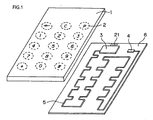
- FIG. 1 is a perspective view illustrating an example of the configuration of a key input apparatus (input apparatus) according to an exemplary embodiment of the present invention.
- the key input apparatus shown in Fig. 1 includes an elastic key sheet (insulating sheet) 1, the main ingredient of which is silicone rubber or the like, and a substrate 6 on which a coplanar line 5 has been formed.
- the key sheet 1 is applied to numeric keys, numerals and the like are printed on one surface of the key sheet 1 and recesses of a conical or cylindrical shape are provided at portions on the other surface that correspond to the numerals, etc., printed on the first-mentioned surface.
- the positions of the recesses provided in one surface of the key sheet 1 correspond to positions 2 of keys of the numerals, etc., printed on the key sheet 1.
- a terminating resistor 4 is placed at one end of the coplanar line 5 on substrate 6, and a microcomputer module 3 is placed at the other end of the coplanar line.
- the coplanar line 5 is formed so as to pass through the vicinity of each key of the numerals, etc., printed on the key sheet 1.
- Interface lines 21 are formed on the substrate 6 for connecting the microcomputer module 3 and other modules, etc.
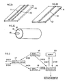
- FIG. 2 is a perspective view illustrating an example of the structure of an electrical signal communication line.
- a coplanar line shown in Fig. 2A includes a signal line 10 formed on one surface of the substrate 6, and a ground line 11 at ground potential disposed in parallel with the signal line 10 and formed so as to have the same cross-sectional area as that of the signal line 10.
- a microstrip line shown in Fig. 2B is a structure in which the signal line 10 is formed on one surface of the substrate 6 and a ground layer 12 at ground potential is formed on the other surface.
- a coaxial line shown in Fig. 2C is a structure in which an internal conductor (signal line) 15 is provided at the center of a cylindrical line, an external conductor 13 is provided at the periphery of the cylindrical line, and the space between the internal conductor 15 and external conductor 13 is filled with a dielectric 14.
- Fig. 3 is a block diagram illustrating an example of the configuration of a portion of the microcomputer module 3 that relates to the sending and receiving of signals and to computation.
- the microcomputer module 3 shown in Fig. 3 includes a directional coupler 17, a signal generator (signal transmitting means) 16, a signal detector (reflected-wave detecting means) 18, a computing unit (computing means) 19 and a memory (storage means) 20.
- TDR Time Domain Reflectometry
- the microcomputer module 3 detects a position at which there is an impedance mismatch in the coplanar line 5, thereby specifying an entered instruction.
- the signal transmitter 16 outputs a signal while varying the frequency from 30 kHz to 3 GHz, by way of example. Further, the signal transmitter 16 outputs transmit-signal strength information, which indicates the strength of the output signal, to the computing unit 19.
- the directional coupler 17 outputs the signal, which has been output by the signal transmitter 16, to the coplanar line 5, and outputs the reflected wave, which has been output from the coplanar line 5, to the signal detector 18.
- the signal detector 18 detects the reflected wave that has been output by the directional coupler 17 and outputs received-signal strength information, which is information indicating the signal strength of the signal included in the reflected wave, to the computing unit 19.
- received-signal strength information which is information indicating the signal strength of the signal included in the reflected wave
- the computing unit 19 computes frequency-domain reflection coefficient and subjects the computed frequency-domain reflection coefficient to an inverse Fourier transform to thereby compute time-domain reflection coefficient.
- frequency-domain reflection coefficient is the ratio of signal strength of the signal included in the reflected wave to signal strength of the signal of each frequency that is output by the signal transmitter 16.
- time-domain reflection coefficient is the rate of change in the reflected wave of the signal output by the signal transmitter 16 with respect to time.
- the memory 20 stores the TDR waveform in a case where there is no impedance mismatch. Further, the memory 20 stores a key map that correlates time from the moment the signal transmitter 16 outputs a signal to the moment an impedance mismatch occurs (namely time it takes for the impedance of the coplanar line 5 to change); distance, which corresponds to this time, from the directional coupler 17 of the microcomputer module 3 to the position at which the impedance mismatch occurred; and the key corresponding to this distance.
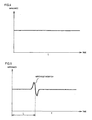
- Fig. 4 is an explanatory view illustrating a TDR waveform in a case where an impedance mismatch has not occurred in the coplanar line 5. If an impedance mismatch has not occurred in the coplanar line 5, a reflected wave of the signal that has been output by the signal transmitter 16 is not produced. If time is plotted along the horizontal axis and impedance along the vertical axis, therefore, as illustrated in Fig. 4 , then a flat TDR waveform is obtained.
- Fig. 5 is an explanatory view illustrating a change in impedance of the coplanar line 5.
- Fig. 6 is an explanatory view illustrating an example of a key map stored by the memory 20.
- impedance changes 2t seconds after the signal transmitter 16 outputs a signal an impedance mismatch occurs at a position whose distance from the microcomputer module 3 is 21 and a "1" key corresponds to this position.
- the characteristic impedance of the coplanar line 5 is decided by the width and thickness of the signal line 10 and ground line 11.
- the signal line 10 and ground line 11 that construct the coplanar line 5 are each formed by a single line in order to make the characteristic impedance uniform. Further, the coplanar line 5 is formed on the substrate 6 in bent fashion taking into consideration the resolution of TDR.
- the path formed by the coplanar line 5 on the substrate 6 will now be described.
- the distance between keys on an ordinary portable terminal is on the order of 10 mm.
- the resolution of TDR must be made less than 10 mm.
- the resolution of TDR is one-fourth of the wavelength of the signal having the highest frequency among signals that are output by the signal transmitter 16. Accordingly, the signal transmitter 16 must output a signal having a frequency of 7.5 GHz.
- the signal may radiate from the coplanar line 5.
- the path of the coplanar line 5 on the substrate 6 is formed in bent fashion to lengthen the distance between keys artificially.
- the coplanar line 5 is formed to have bent portions in order to lengthen the distance between the portions that pass through the vicinity of each of the keys in the key sheet 1.
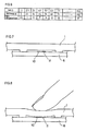
- Fig. 7 is an explanatory view illustrating the cross section of the substrate 6 and key sheet 1.
- the signal line 10 and ground line 11 are formed on the surface of the substrate 6 that faces the key sheet 1.
- the widths and heights of the conductor portions of the signal line 10 and ground line 11 are uniform. It should be noted that the widths and heights of the conductor portions of the signal line 10 and ground line 11 and the cross-sectional shape of the key sheet 1 in the vicinity of the signal line 10 are set in such a manner that the characteristic impedance of the coplanar line 5 (see Fig. 1 ) will be the same at any portion whatsoever. In other words, if the key sheet 1 is not pressed, an impedance mismatch is not produced in the coplanar line 5 comprising the signal line 10 and ground line 11.
- Fig. 8 is an explanatory view illustrating a cross section of the sheet key 1 that is being pressed.
- the key sheet 1 which is a dielectric
- the coplanar line 5 (see Fig. 1 ) comprising the signal line 10 and ground line 11 so that dielectric constant at the periphery of the signal line changes.
- An impedance mismatch is produced in the coplanar line as a result.
- a reflected wave of the signal that has been output by the microcomputer module 3 (see Fig. 1 ) is produced at the position on the coplanar line 5 where the impedance mismatch is produced.
- the reflected wave of the signal that has been output by the microcomputer module 3 advances toward the microcomputer module 3 through the coplanar line 5.
- the signal transmitter 16 varies frequency continuously from low frequency (e.g., 30 kHz) to high frequency (e.g., 3 GHz) and outputs a signal at all times (step S101).
- the signal transmitter 16 outputs transmit-signal strength information, which indicates the strength of the output signal, to the computing unit 19 (step S102).
- the directional coupler 17 outputs the signal, which has been output by the signal transmitter 16, to the coplanar line 5 (step S103. If an impedance mismatch has been produced in the coplanar line 5 (see Fig. 1 ), a reflected wave is output from the coplanar line 5 to the directional coupler 17 (step S104).
- the directional coupler 17 outputs the output reflected wave to the signal detector 18 (step S105).
- the signal detector 18 detects the reflected wave that has been output by the directional coupler 17 and outputs received-signal strength information, which is information indicating the signal strength of the signal included in the reflected wave, to the computing unit 19 (step S106).
- the computing unit 19 of Fig. 3 computes frequency-domain reflection coefficient based upon the transmit-signal strength information output by the signal transmitter 16 and received-signal strength information output by the signal detector 18.
- the computing unit 19 subjects the computed frequency-domain reflection coefficient to an inverse Fourier transform and obtains the result of TDR (the TDR waveform).
- a reflected wave of the signal that has been output by the signal transmitter 16 is produced. If time is plotted along the horizontal axis and impedance along the vertical axis, therefore, as illustrated in Fig. 5 , then a TDR waveform indicating a change in impedance is obtained.
- the time it takes for the TDR waveform of Fig. 5 to indicate a change in impedance is proportional to the distance between the position at which impedance mismatch occurred and the directional coupler 17 of the microcomputer module 3. Therefore, by referring to the key map stored in the memory 20 exemplified in Fig. 6 , the computing unit 19 is capable of discriminating which key has been pressed based upon the time it takes for the TDR waveform to indicate a change in impedance (steps S107, S108 shown in Fig. 3 ).
- the computing unit 19 specifies the entered instruction based upon the result of discrimination.
- the computing unit 19 outputs information indicating the instruction (key) specified and entered (pressed) to control means of a portable terminal or the like on which the input apparatus has been mounted.
- the key input apparatus is constructed by the substrate 6, on which the coplanar line 5 has been formed, and the flexible key sheet 1. Accordingly, dome-shaped recesses of the kind shown in Fig. 11 are unnecessary. This makes it possible to reduce the thickness of the key input apparatus.
- which key has been pressed is determined based upon a change in the impedance of the coplanar line 5 formed on the substrate 6. This makes it unnecessary to provide another device or the like below the keys and makes it possible to reduce the thickness of the key input apparatus.
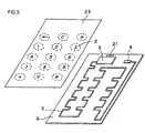
- FIG. 9 is a perspective view illustrating the key input apparatus in a case where, instead of the key sheet 1, film 23 on which key positions have been indicated has been placed on the surface of the substrate 6 on which the coplanar line 5 has been formed.
- the film 23 on which the key positions have been indicated is placed on the surface of the substrate 6 on which the coplanar line 5 has been formed, a greater reduction in the thickness of the key input apparatus can be achieved in comparison with the case where the key sheet 1 is used. It is desired that the film 23 have a high durability.
- the coplanar line 5 may have a portion 22 formed into a circle.
- Fig. 10 is a perspective view illustrating a key input apparatus in which a portion of the coplanar line 5 has been formed into a circle. If the portion of the key sheet 1 corresponding to the portion 22 of the coplanar line 5 formed into a circle is traced with a finger, then an impedance mismatch is produced at the portion traced. The position at which the impedance mismatch is produced changes depending upon the motion of the finger. Consequently, if the microcomputer module 3 discriminates motion of the finger based upon a change in the position at the impedance mismatch occurred, then the key input apparatus can be equipped with a disk-shaped operating portion.
- discrimination by the computing unit (computing means) 19 of an operated operating position based upon a reflected wave detected by the signal detector (reflected-wave detecting means) 18 means that the computing unit 19 measures the time it takes for the signal detector 18 to detect a reflected wave and computes the distance between the signal detector 18 and the operated operating position based upon the measured time, thereby discriminating the operated operating position.
- the discrimination by the computing unit 19 of an operated operating position based upon the signal strength of the signal output by the signal generator (signal transmitting means) 16 and the signal strength of the reflected wave detected by the signal detector (reflected-wave detecting means) 18 means that the computing unit 19 compares the signal strength of the signal output by the signal transmitter 16 and the signal strength of the reflected wave detected by the signal detector (reflected-wave detecting means) 18, determines that the signal detector 18 has detected a reflected wave at a timing at which the signal detector 18 has detected a signal having a signal strength different from a signal strength of the signal which has been output by the signal transmitter 16, and computes the distance between the signal detector 18 and the operating position where the operation has been done based upon the time it takes for the signal detector 18 to detect the reflected wave, thereby discriminating the operating position where the operation has been done.
- Carrying out measurement of time domain reflection coefficient by the computing unit 19 based upon the signal strength of the signal that has been output by the signal transmitter 16 and the signal strength of the reflected wave detected by the signal detector 18 means that the computing unit 19 compares the signal strength of the signal that has been output by the signal transmitter 16 as frequency is changed and the signal strength of the signal of each frequency included in the reflected wave detected by the signal detector 18, computes the frequency-domain reflection coefficient, subjects the computed frequency-domain reflection coefficient to an inverse Fourier transform and carries out time domain reflection coefficient.
- the discrimination by the computing unit 19 of an operated operating position based upon the TDR result, namely the result of measurement of the time domain reflection coefficient, means that the computing unit 19 computes the distance between the signal detector 18 and the operated operating position based upon the timing at which the time-domain reflection coefficient changes, thereby discriminating the operated operating position.
- the identification by the computing unit 19 of an entered instruction based upon the table stored by the storage means and the TDR result means that the computing unit 19 refers to the table correlating timings at which time-domain reflection coefficient changed and entered instructions and determines that an instruction corresponding to a timing at which time-domain reflection coefficient changed is an entered instruction.
- the present invention can be utilized in an input apparatus of a portable terminal or the like.
Landscapes
- Engineering & Computer Science (AREA)
- General Engineering & Computer Science (AREA)
- Theoretical Computer Science (AREA)
- Human Computer Interaction (AREA)
- Physics & Mathematics (AREA)
- General Physics & Mathematics (AREA)
- Push-Button Switches (AREA)
- Input From Keyboards Or The Like (AREA)
- Telephone Set Structure (AREA)
Claims (7)
- Appareil d'entrée qui comprend un substrat (6) sur une surface duquel une ligne de signaux (10) est formée, et une feuille isolante (1) disposée en regard de la surface du substrat (6) et ayant des informations, qui représentent une pluralité de positions de fonctionnement à appuyer, affichées sur sa surface qui est sur un côté opposé à une surface faisant face au substrat (6), l'appareil étant caractérisé en ce qu'il a :la ligne de signaux (10) et une ligne de terre (11) au potentiel de la terre, qui est formée en parallèle avec la ligne de signaux (10), sont formées sur le substrat (6) afin de traverser le voisinage des positions de fonctionnement dans la feuille isolante (1), et de s'étendre en série d'une desdites positions de fonctionnement à une autre desdites positions de fonctionnement, et d'avoir des parties courbées sur le substrat (6) au niveau de parties qui traversent le voisinage de la partie sur la feuille isolante (1) à laquelle des parties de fonctionnement sont disposées afin d'allonger la distance entre les parties qui traversent le voisinage de chacune des positions de fonctionnement disposées sur ladite feuille isolante (1) ;des moyens de transmission de signal (16) pour sortir un signal vers la ligne de signaux (10) ;des moyens de détection d'onde réfléchie (18) pour détecter une onde réfléchie du signal sorti par les moyens de transmission de signal (16) ; etdes moyens de calcul (19) pour discriminer une position de fonctionnement au niveau de laquelle une opération d'appui a été effectuée, sur la base de l'onde réfléchie détectée par les moyens de détection d'onde réfléchie (18).
- Appareil d'entrée selon la revendication 1, dans lequel la ligne de signaux (10) a des parties courbées sur le substrat (16) au niveau de parties qui traversent le voisinage de la partie sur la feuille isolante (1) à laquelle des touches sont affectées.
- Appareil d'entrée selon la revendication 1 ou 2, dans lequel les moyens de calcul (19) discriminent une position de fonctionnement au niveau de laquelle une opération d'appui a été effectuée, sur la base de l'intensité de signal du signal sorti par les moyens de transmission de signal (16) et de l'intensité de signal de l'onde réfléchie détectée par les moyens de détection d'onde réfléchie (18).
- Appareil d'entrée selon la revendication 1 ou 2, dans lequel les moyens de calcul (19) effectuent la mesure d'un coefficient de réflexion dans le domaine temporel sur la base de l'intensité de signal du signal sorti par les moyens de transmission de signal (16) et de l'intensité de signal de l'onde réfléchie détectée par les moyens de détection d'onde réfléchie (18), et discriminent une position de fonctionnement au niveau de laquelle une opération d'appui a été effectuée, sur la base d'un résultat de TDR qui est le résultat de la mesure du coefficient de réflexion dans le domaine temporel.
- Appareil d'entrée selon la revendication 4, comprenant en outre des moyens de stockage (20) dans lesquels une table corrélant le résultat de TDR et des instructions introduites est stockée à l'avance ;
dans lequel les moyens de calcul (19) spécifient une instruction introduite sur la base de la table stockée par les moyens de stockage (20) et du résultat de TDR. - Appareil d'entrée selon la revendication 4 ou 5, dans lequel la ligne de signaux (10) est formée sur le substrat (6) afin d'avoir une partie circulaire (22) ; et
les moyens de calcul (19) discriminent une opération d'appui qui a été effectuée sur la feuille isolante (1), sur la base d'un changement du résultat. - Procédé d'entrée utilisant un appareil d'entrée comprenant un substrat (6) sur une surface duquel une ligne de signaux (10) a été formée, et une feuille isolante (1) disposée en regard de la surface du substrat (6) et ayant des informations, qui représentent une pluralité de positions de fonctionnement à appuyer, affichées sur sa surface qui est sur un côté opposé à une surface faisant face au substrat (6), la ligne de signaux (10) et une ligne de terre (11) au potentiel de la terre, qui est formée en parallèle avec la ligne de signaux (10), sont formées sur le substrat (6) afin de traverser le voisinage des positions de fonctionnement dans la feuille isolante (1), et de s'étendre en série d'une desdites positions de fonctionnement à une autre desdites positions de fonctionnement, et d'avoir des parties courbées sur le substrat (6) au niveau de parties qui traversent le voisinage de la partie sur la feuille isolante (1) à laquelle des parties de fonctionnement sont disposées afin d'allonger la distance entre les parties qui traversent le voisinage de chacune des positions de fonctionnement disposées sur ladite feuille isolante (1) ;
le procédé comprenant :une étape de sortie de signal de moyens de transmission de signal (16) sortant un signal vers la ligne de signaux (10) ;une étape de détection d'onde réfléchie de moyens de détection d'onde réfléchie (18) détectant une onde réfléchie du signal sorti par les moyens de transmission de signal (16) à l'étape de sortie de signal ; etune étape de calcul de moyens de calcul (19) discriminant une position de fonctionnement au niveau de laquelle une opération d'appui a été effectuée, sur la base de l'onde réfléchie détectée par les moyens de détection d'onde réfléchie (18) à l'étape de détection d'onde réfléchie.
Applications Claiming Priority (2)
| Application Number | Priority Date | Filing Date | Title |
|---|---|---|---|
| JP2006091791 | 2006-03-29 | ||
| PCT/JP2007/056177 WO2007111291A1 (fr) | 2006-03-29 | 2007-03-26 | Appareil et procede de saisie |
Publications (3)
| Publication Number | Publication Date |
|---|---|
| EP2000887A1 EP2000887A1 (fr) | 2008-12-10 |
| EP2000887A4 EP2000887A4 (fr) | 2010-07-28 |
| EP2000887B1 true EP2000887B1 (fr) | 2013-07-17 |
Family
ID=38541208
Family Applications (1)
| Application Number | Title | Priority Date | Filing Date |
|---|---|---|---|
| EP07739615.8A Not-in-force EP2000887B1 (fr) | 2006-03-29 | 2007-03-26 | Appareil et procede de saisie |
Country Status (5)
| Country | Link |
|---|---|
| US (1) | US8286489B2 (fr) |
| EP (1) | EP2000887B1 (fr) |
| JP (1) | JP5298848B2 (fr) |
| CN (1) | CN101395560B (fr) |
| WO (1) | WO2007111291A1 (fr) |
Families Citing this family (18)
| Publication number | Priority date | Publication date | Assignee | Title |
|---|---|---|---|---|
| US8599155B2 (en) | 2010-04-30 | 2013-12-03 | Microchip Technology Incorporated | Touch sense using time domain reflectometry |
| CN102012786A (zh) * | 2010-11-15 | 2011-04-13 | 中兴通讯股份有限公司 | 按键实现方法、按键系统及移动终端 |
| US8972214B2 (en) | 2011-04-21 | 2015-03-03 | Microchip Technology Incorporated | Touch sense determined by characterizing impedance changes in a transmission line |
| TWI581135B (zh) * | 2011-09-30 | 2017-05-01 | 加拿都公司 | 觸感薄膜、觸感裝置及電子裝置 |
| US20140132523A1 (en) * | 2012-11-13 | 2014-05-15 | David Brent GUARD | Touch Sensing Based On Signal Reflections |
| US10067607B2 (en) * | 2014-01-17 | 2018-09-04 | Lg Innotek Co., Ltd. | Time domain reflectometry touch window sensor |
| KR102152857B1 (ko) * | 2014-05-08 | 2020-09-07 | 엘지이노텍 주식회사 | 터치 윈도우 |
| US10261631B2 (en) | 2014-05-08 | 2019-04-16 | Lg Innotek Co., Ltd. | Electronic device |
| KR102175668B1 (ko) * | 2014-05-14 | 2020-11-06 | 엘지이노텍 주식회사 | 전자 장치 |
| JP2016180747A (ja) * | 2015-03-24 | 2016-10-13 | パナソニックIpマネジメント株式会社 | 感圧センサ |
| CN106406646A (zh) * | 2016-09-19 | 2017-02-15 | 广州视源电子科技股份有限公司 | Tdr扫描式触摸屏及触摸扫描定位方法 |
| CN106468974B (zh) * | 2016-09-19 | 2020-03-17 | 广州视源电子科技股份有限公司 | 触摸屏校准方法及触摸扫描定位方法 |
| CN106383622A (zh) * | 2016-09-19 | 2017-02-08 | 广州视源电子科技股份有限公司 | Tdr扫描式触摸屏、触摸扫描定位方法及触控液晶显示屏 |
| CN106249962A (zh) * | 2016-09-19 | 2016-12-21 | 广州视源电子科技股份有限公司 | Tdr扫描式触控屏及触控定位方法 |
| CN106371668A (zh) * | 2016-09-19 | 2017-02-01 | 广州视源电子科技股份有限公司 | 触摸物形状识别方法、装置及触摸屏 |
| CN106354330B (zh) * | 2016-09-19 | 2020-07-28 | 广州视源电子科技股份有限公司 | 基于用户输入压力的触屏响应方法及装置 |
| CN106406649A (zh) * | 2016-09-19 | 2017-02-15 | 广州视源电子科技股份有限公司 | Tdr触摸屏及触摸扫描定位方法 |
| CN106371683A (zh) * | 2016-09-19 | 2017-02-01 | 广州视源电子科技股份有限公司 | Tdr触控屏及触控定位方法 |
Family Cites Families (11)
| Publication number | Priority date | Publication date | Assignee | Title |
|---|---|---|---|---|
| US5149918A (en) | 1990-10-29 | 1992-09-22 | International Business Machines Corporation | Touch sensitive overlay |
| JP2964667B2 (ja) | 1991-03-04 | 1999-10-18 | 株式会社スリーボンド | 異材質複合射出成形装置 |
| JPH054254U (ja) * | 1991-07-02 | 1993-01-22 | 横河電機株式会社 | 入力装置 |
| TW241352B (en) | 1994-03-30 | 1995-02-21 | Whitaker Corp | Reflective mode ultrasonic touch sensitive switch |
| JPH11194883A (ja) * | 1998-01-06 | 1999-07-21 | Poseidon Technical Systems:Kk | タッチ操作型コンピュータ |
| US6137282A (en) | 1998-06-25 | 2000-10-24 | Becs Technology, Inc. | Time-domain reflectometry user input device |
| CN100374988C (zh) * | 2000-09-22 | 2008-03-12 | 北京青谷科技有限公司 | 超声波手写键盘 |
| US20050088417A1 (en) * | 2003-10-24 | 2005-04-28 | Mulligan Roger C. | Tactile touch-sensing system |
| US8184108B2 (en) * | 2004-06-30 | 2012-05-22 | Poa Sana Liquidating Trust | Apparatus and method for a folded optical element waveguide for use with light based touch screens |
| US7412119B2 (en) * | 2004-06-30 | 2008-08-12 | Poa Sana Liquidating Trust | Apparatus and method for making flexible waveguide substrates for use with light based touch screens |
| CN101432647B (zh) * | 2006-05-01 | 2013-01-30 | Rpo私人有限公司 | 用于光学触摸屏的波导材料 |
-
2007
- 2007-03-26 CN CN200780007254.4A patent/CN101395560B/zh not_active Expired - Fee Related
- 2007-03-26 EP EP07739615.8A patent/EP2000887B1/fr not_active Not-in-force
- 2007-03-26 JP JP2008507484A patent/JP5298848B2/ja not_active Expired - Fee Related
- 2007-03-26 US US12/281,199 patent/US8286489B2/en not_active Expired - Fee Related
- 2007-03-26 WO PCT/JP2007/056177 patent/WO2007111291A1/fr not_active Ceased
Also Published As
| Publication number | Publication date |
|---|---|
| EP2000887A1 (fr) | 2008-12-10 |
| CN101395560A (zh) | 2009-03-25 |
| EP2000887A4 (fr) | 2010-07-28 |
| WO2007111291A1 (fr) | 2007-10-04 |
| US8286489B2 (en) | 2012-10-16 |
| JP5298848B2 (ja) | 2013-09-25 |
| CN101395560B (zh) | 2013-07-24 |
| JPWO2007111291A1 (ja) | 2009-08-13 |
| US20090013788A1 (en) | 2009-01-15 |
Similar Documents
| Publication | Publication Date | Title |
|---|---|---|
| EP2000887B1 (fr) | Appareil et procede de saisie | |
| US9563316B2 (en) | Radiofrequency-wave-transparent capacitive sensor pad | |
| US7784366B2 (en) | Single sided capacitive force sensor for electronic devices | |
| TWI429882B (zh) | A position detecting device and a display device | |
| US20160283006A1 (en) | Pressure sensor including time-domain reflectometer | |
| EP0483519A1 (fr) | Couche à redéfinition de fonctions sensible au toucher | |
| CN113454581B (zh) | 触控基板及显示装置 | |
| US10509514B2 (en) | Touch device capable of detecting touch events through vibration | |
| KR101410175B1 (ko) | 터치 키를 구비한 휴대용 통신 장치 | |
| US20220137776A1 (en) | Touch control method, circuit system, and touch device | |
| US20220137775A1 (en) | Touch control method, circuit system and touch device | |
| KR20190098889A (ko) | 표시 장치 | |
| CN101859211B (zh) | 手指触控定位装置及方法 | |
| CN113703618A (zh) | 旋钮式触控显示装置及其驱动方法 | |
| JP2004022356A (ja) | タッチスイッチ | |
| US5923101A (en) | Non-contact key | |
| US20060002203A1 (en) | Input device having activating means | |
| US11994761B2 (en) | Ground feature in a capacitive touch system | |
| US11983373B1 (en) | Filter in a capacitance measuring circuit | |
| CN112398546B (zh) | 电子装置 | |
| CN214529778U (zh) | 洗衣机 | |
| CN113687740A (zh) | 电容式触摸感应板及具有其的电器 | |
| US10235004B1 (en) | Touch input detector with an integrated antenna | |
| KR102337904B1 (ko) | 터치센서 모듈 및 이를 이용하는 전자 기기 | |
| CN212276393U (zh) | 电容式触摸感应板及具有其的电器 |
Legal Events
| Date | Code | Title | Description |
|---|---|---|---|
| PUAI | Public reference made under article 153(3) epc to a published international application that has entered the european phase |
Free format text: ORIGINAL CODE: 0009012 |
|
| 17P | Request for examination filed |
Effective date: 20080819 |
|
| AK | Designated contracting states |
Kind code of ref document: A1 Designated state(s): DE FR GB IT |
|
| DAX | Request for extension of the european patent (deleted) | ||
| RBV | Designated contracting states (corrected) |
Designated state(s): DE FR GB IT |
|
| A4 | Supplementary search report drawn up and despatched |
Effective date: 20100628 |
|
| 17Q | First examination report despatched |
Effective date: 20100712 |
|
| GRAP | Despatch of communication of intention to grant a patent |
Free format text: ORIGINAL CODE: EPIDOSNIGR1 |
|
| GRAP | Despatch of communication of intention to grant a patent |
Free format text: ORIGINAL CODE: EPIDOSNIGR1 |
|
| GRAS | Grant fee paid |
Free format text: ORIGINAL CODE: EPIDOSNIGR3 |
|
| GRAA | (expected) grant |
Free format text: ORIGINAL CODE: 0009210 |
|
| AK | Designated contracting states |
Kind code of ref document: B1 Designated state(s): DE FR GB IT |
|
| REG | Reference to a national code |
Ref country code: GB Ref legal event code: FG4D |
|
| REG | Reference to a national code |
Ref country code: DE Ref legal event code: R096 Ref document number: 602007031702 Country of ref document: DE Effective date: 20130912 |
|
| PLBE | No opposition filed within time limit |
Free format text: ORIGINAL CODE: 0009261 |
|
| STAA | Information on the status of an ep patent application or granted ep patent |
Free format text: STATUS: NO OPPOSITION FILED WITHIN TIME LIMIT |
|
| PG25 | Lapsed in a contracting state [announced via postgrant information from national office to epo] |
Ref country code: IT Free format text: LAPSE BECAUSE OF FAILURE TO SUBMIT A TRANSLATION OF THE DESCRIPTION OR TO PAY THE FEE WITHIN THE PRESCRIBED TIME-LIMIT Effective date: 20130717 |
|
| 26N | No opposition filed |
Effective date: 20140422 |
|
| REG | Reference to a national code |
Ref country code: DE Ref legal event code: R097 Ref document number: 602007031702 Country of ref document: DE Effective date: 20140422 |
|
| REG | Reference to a national code |
Ref country code: GB Ref legal event code: 732E Free format text: REGISTERED BETWEEN 20141023 AND 20141029 |
|
| REG | Reference to a national code |
Ref country code: FR Ref legal event code: TP Owner name: LENOVO INNOVATIONS LIMITED (HONG KONG), HK Effective date: 20141119 |
|
| REG | Reference to a national code |
Ref country code: FR Ref legal event code: PLFP Year of fee payment: 10 |
|
| PGFP | Annual fee paid to national office [announced via postgrant information from national office to epo] |
Ref country code: DE Payment date: 20160322 Year of fee payment: 10 |
|
| PGFP | Annual fee paid to national office [announced via postgrant information from national office to epo] |
Ref country code: FR Payment date: 20160208 Year of fee payment: 10 Ref country code: GB Payment date: 20160323 Year of fee payment: 10 |
|
| REG | Reference to a national code |
Ref country code: DE Ref legal event code: R119 Ref document number: 602007031702 Country of ref document: DE |
|
| GBPC | Gb: european patent ceased through non-payment of renewal fee |
Effective date: 20170326 |
|
| REG | Reference to a national code |
Ref country code: FR Ref legal event code: ST Effective date: 20171130 |
|
| PG25 | Lapsed in a contracting state [announced via postgrant information from national office to epo] |
Ref country code: DE Free format text: LAPSE BECAUSE OF NON-PAYMENT OF DUE FEES Effective date: 20171003 Ref country code: FR Free format text: LAPSE BECAUSE OF NON-PAYMENT OF DUE FEES Effective date: 20170331 |
|
| PG25 | Lapsed in a contracting state [announced via postgrant information from national office to epo] |
Ref country code: GB Free format text: LAPSE BECAUSE OF NON-PAYMENT OF DUE FEES Effective date: 20170326 |