EP1999456B1 - Thz-antennen-array, system und verfahren zur herstellung eines thz-antennen-arrays - Google Patents
Thz-antennen-array, system und verfahren zur herstellung eines thz-antennen-arrays Download PDFInfo
- Publication number
- EP1999456B1 EP1999456B1 EP07723734.5A EP07723734A EP1999456B1 EP 1999456 B1 EP1999456 B1 EP 1999456B1 EP 07723734 A EP07723734 A EP 07723734A EP 1999456 B1 EP1999456 B1 EP 1999456B1
- Authority
- EP
- European Patent Office
- Prior art keywords
- thz
- region
- antenna array
- photoconductive
- thz antenna
- Prior art date
- Legal status (The legal status is an assumption and is not a legal conclusion. Google has not performed a legal analysis and makes no representation as to the accuracy of the status listed.)
- Not-in-force
Links
Images


Classifications
-
- H—ELECTRICITY
- H01—ELECTRIC ELEMENTS
- H01Q—ANTENNAS, i.e. RADIO AERIALS
- H01Q9/00—Electrically-short antennas having dimensions not more than twice the operating wavelength and consisting of conductive active radiating elements
- H01Q9/005—Electrically-short antennas having dimensions not more than twice the operating wavelength and consisting of conductive active radiating elements for radiating non-sinusoidal waves
-
- Y—GENERAL TAGGING OF NEW TECHNOLOGICAL DEVELOPMENTS; GENERAL TAGGING OF CROSS-SECTIONAL TECHNOLOGIES SPANNING OVER SEVERAL SECTIONS OF THE IPC; TECHNICAL SUBJECTS COVERED BY FORMER USPC CROSS-REFERENCE ART COLLECTIONS [XRACs] AND DIGESTS
- Y10—TECHNICAL SUBJECTS COVERED BY FORMER USPC
- Y10T—TECHNICAL SUBJECTS COVERED BY FORMER US CLASSIFICATION
- Y10T29/00—Metal working
- Y10T29/49—Method of mechanical manufacture
- Y10T29/49002—Electrical device making
- Y10T29/49016—Antenna or wave energy "plumbing" making
Definitions
- the invention relates to a THz antenna array having a number of THz antennas, wherein a THz antenna has a photoconductive region and a first electrode and a second electrode, which are spaced over a distance range extending laterally over at least one part of the photoconductive region.
- the invention further relates to a method for producing a THz antenna array having a number of THz antennas, wherein a THz antenna has a photoconductive region and a first electrode and a second electrode, which are spaced apart over a distance range, which is located extends laterally over at least a portion of the photoconductive region.
- THz antennas can be formed and fabricated in a variety of ways, including such. can be used as a receiver and / or as a transmitter.
- a first fundamental form of a THz antenna provides a semi-large antenna single structure, which is designed in the range between microscopic structures (below 100 ⁇ m) and macroscopic millimeter structures (> 1 mm).
- Such a THz antenna is of Stone et.al. in the article "Electrical and Radiation Characteristics of Semiconductor Photoconductive Terahertz Emitters" in IEEE TRANSACTIONS ON MICROWAVE THEORY AND TECHNIQUES, Vol. 52, no. 10, October 2004 , described.
- US 5,401,953 discloses an integrated submillimeter radiation generation device, the device comprising an array of N photoconductive switches biased by a common voltage source and having an optical path difference from a common optical pulse at a repetition rate provides different optical delay for each of the switches.
- the triggering of the N-switches takes place via a pulse traveling along the entire array of N-switches up to a single antenna, which radiates submillimeter radiation spherically in all directions as a point source.
- THz antenna arrays of the type mentioned in the beginning of a number of THz antennas or THz antenna structures have improved performance and modulability thereof as well as an improved directional characteristic.
- a THz antenna or THz antenna structure basically has two spaced apart electrodes with an intervening photoconductive material, i. As a rule, an area with semiconducting material in which optical charge carriers can be generated on.
- the individual THz antennas or THz antenna structures usually have microscopic dimensions.
- the problem here is the decoupling of the individual THz antennas as elements of the array in order to avoid destructive interference of the THz far field - usually, for. in finger structures, adjacent elements of the array, e.g. two fingers each with intervening photoconductive material, biased against opposite polarity. For this purpose, different possibilities for decoupling the individual elements of the array have hitherto been provided.
- the disadvantage here is that the production of such structures is comparatively complicated, since, inter alia, two additional layers of material for optical partitioning of suitable areas of the THz antenna array must be deposited - this is at least an electrical insulation layer for the isolation of electrodes of adjacent THz antennas and an opaque layer to be deposited thereon, which is usually made of a metal layer.
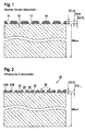
- a cross-sectional view of such a THz antenna array is shown in FIG Fig. 1 specified.
- the additional optically isolating layers mentioned there can fundamentally adversely affect the performance of the antenna arrangement. It has been shown that the dark current is comparatively high, since in the sealed-off regions of the THz antenna array usually More than 50% of the total dark current is generated. This leads to a higher energy consumption of the THz antenna array in the case of a THz emitter or to a lower sensitivity in the case of a THz detector. In addition, the production of such an array has proven to be comparatively expensive.
- the invention begins, whose object is to provide a THz antenna array and a manufacturing method, which has improved properties, in particular simplified compared to the known arrays and manufacturing method.
- the object is achieved by the invention by means of the THz antenna array of the type mentioned above, wherein according to the invention a lateral region between adjacent THz antennas of the array is formed virtually non-photoconductive, i. A photoconductivity may or may not be present compared to a portion of a THz antenna or is negligibly small.
- a lateral area between adjacent THz antennas of the array is virtually free of photoconductive material.
- adjacent THz active elements of the array i. THz antennas or structures are per se isolated from each other in terms of photoconductivity - unlike conventional structures of the type described above, in which also areas between adjacent THz-active elements are photoconductive.
- the concept of the invention thus provides for a direct decoupling of the THz-active elements of the array, ie the THz antennas or THz antenna structures, according to which a lateral area between adjacent THz antennas of the array is formed virtually non-photoconductive.
- the invention has recognized that thereby an optical generation of photoconductive charge carriers in the lateral region between adjacent THz antennas of the array per se is impossible or negligible, so that in these areas per se no THz radiation can take place, the one to could contribute to destructive far-field interference.
- additional measures of antenna decoupling such as the location-dependent modulation of the optical excitation, whether by binary gratings, frequency mixing, or an optical isolation of the lateral areas between adjacent THz antennas, can advantageously be omitted.
- the invention provides that a part of the photoconductive region in the lateral region between adjacent THz antennas of the array is removed, in particular completely removed.
- a corresponding THz antenna array has, in particular, a photoconductive region which points to a limited lateral extent, which does not significantly beyond the lateral extent of the distance range or over the lateral extent of the distance range and the electrodes.
- the THz antenna arrays provided in accordance with the inventive concept and the corresponding production method use in an inventive manner the principle of the epitaxial lift-off method using comparatively thin photoconductive films.
- the elements of the array forming THz radiation emitting or detecting structures according to the concept of the invention can thus be particularly flexible and adapt with little effort and without additional components to a variety of optical systems with full-surface optical excitation. It has been shown that the emission power or detection sensitivity is optimized in comparison to previously known THz antenna arrays. It has been found that a THz antenna array according to the concept of the invention generally has a dark current reduced by at least 50%, which additionally increases the consumption or the sensitivity of a detector. In addition, the aforementioned disadvantages of the prior art are largely avoided. Should be in the context of special applications nevertheless an additional location-dependent modulation of the optical excitation be desired, the proposed concept offers the advantage of an increased tolerance range for adjusting an optical frequency mixing excitation or a binary grating. Additional optically isolating layers of material are generally not necessary. The production of the THz antenna array according to the concept of the invention can be realized in a particularly effective and cost-effective manner.
- a semiconductor material as a carrier substrate is basically no longer mandatory. It can be used in the context of developments carrier substrates, which have optimized properties for a corresponding application.
- a lateral area between adjacent THz antennas of the array in the THz frequency range is comparatively low in absorption and / or dispersion.
- a lateral region between adjacent THz antennas of the array may also be optically transparent and / or non-conductive. The electrical losses or dispersion effects can advantageously be largely avoided both in the THz frequency range and in the optical range.
- the lateral region between adjacent THz antenna arrays is formed by means of a substrate, in particular by means of a sapphire or quartz glass substrate.
- a substrate in particular by means of a sapphire or quartz glass substrate.
- the substrate does not necessarily have to be optically transparent, for example, undoped silicon is also suitable, since it is comparatively low in absorption and / or dispersion in the THz range.
- the lateral area between adjacent THz antennas - in particular at a deposition height of the photoconductive area and / or the electrodes - is material-free, i. a lateral area between adjacent THz antennas of the array is virtually completely removed during the manufacturing process.
- a THz antenna array according to the concept, in particular according to the cited developments of the invention are advantageously designed for collective impulsive optical excitation in the photoconductive region optimized, preferably - depending on the photoconductive material - at an energy above from 0.9 eV.
- the optical excitation is preferably carried out by means of a femtosecond laser pulse, in particular in a wavelength range between 650 nm to 1200 nm, preferably between 750 nm and 850 nm.
- a THz antenna by means of a metal-semiconductor-metal structure (MSM structure) formed in which the electrodes as a metal and the photoconductive region is formed as a semiconductor.
- MSM structure metal-semiconductor-metal structure
- the photoconductive region is particularly advantageously formed by means of LT-GaAs. The properties of the conductor carriers in the photoconductive region which are relevant for the THz radiation emission or detection are thereby advantageously adjustable.
- the photoconductive region has at least one pho- toconductive layer arranged below the electrodes, in particular a layer which extends over the lateral extent of the spacer region and the electrodes.
- the photoconductive region has at least one photoconductive layer, optionally only between the electrodes, in particular a layer which optionally extends only over the lateral extent of the distance region.
- the photoconductive region is advantageously limited to a thickness of 10 ⁇ m, preferably 5 ⁇ m, preferably 2 ⁇ m, preferably 1 ⁇ m. In particular, it has been found that the photoconductive region advantageously has a thickness of at least 0.5 ⁇ m.
- THz antennas which are formed by means of electrodes in the form of a finger structure.
- a finger of the finger structure may have a geometry that contributes to the formation of a THz resonator. So resonant peaks of certain THz frequency ranges can be achieved.
- the finger of the finger structure particularly advantageously has in its lateral extent a T-shaped geometry pointing away from the photoconductive region.
- At least a first number of THz antennas can be at different potential compared to a second number of THz antennas. This opens up an additional possibility of radiation modulation by potential control of the THz antennas.
- the invention also leads to a system comprising a number of THz antenna arrays of the type described above, in which at least a first number of THz antenna arrays have different potentials compared to a second number of THz Antenna array is located.
- THz antenna arrays can be found in the further subclaims and serve above all to increase the efficiency. This can be achieved alone or in combination of different measures in the array design and / or antenna design, the optical excitation improvement and a functionalization of the layers and / or surfaces of the THz antenna array and / or the THz antenna.
- a distance of THz antennas is chosen comparatively large, in particular at ⁇ / 2 .
- a microlens or microlens array may be provided for focusing and aligning the optical excitation.
- a functionalized array of high-permittivity nanoparticles can serve for field enhancement.
- metal layers can be deposited by means of evaporation within the framework of the electrode structuring and a lifting off of unnecessary electrodic areas can take place.
- the electrode structuring can also take place by means of chemical etching of non-required electrodic areas.
- the photoconductive region is limited to a lateral extent that does not significantly exceed the lateral extent of the spacer region or the lateral extent of the spacer region and the electrodes.
- the removal of the portion of the photoconductive region is accomplished by chemical etching of a lateral region between adjacent THz antennas of the array.
- the lifting of the resulting structure of the THz antenna array from the starting material is advantageously carried out by means of chemical etching of a sacrificial region below the photoconductive region.
- Fig. 1 shows a schematic cross-sectional view of a known THz emitter according to the aforementioned article by Dreysburg et al.
- Two interdigitated finger electrodes 11 are processed by means of optical lithography on the surface of a semiconducting GaAs wafer 12.
- the distances of the fingers of the finger electrode 11 are 5 microns.
- the metallization of a finger electrode 11 consists of 5 nm chromium and 200 nm gold.
- An opaque further metallization in the form of an optically transparent metal layer 14 of chrome-gold covers every second finger electrode spacing.
- This second metal layer 14 is isolated from the first metal layer of the finger electrode 11 by an insulating layer 13 in the form of a polyimide layer of about 2 ⁇ m or a silicon oxide layer of 560 nm thickness.
- the substrate in the form of the GaAs wafer 12 has a thickness of about 500 ⁇ m.
- a THz antenna array 20, 30, 40 in which a lateral area between adjacent THz antennas is formed virtually non-photoconductive, that is, a photoconductor compared to a range of a THz antenna can not be or is or is negligible. This will be how based on Fig. 1 to Fig. 8 described, achieved in that a lateral area between adjacent THz antennas is free of photoconductive material.
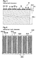
- FIG. 2 shows a THz antenna array 20 in cross section, with a number of THz antennas 29, wherein a THz antenna 29 has a photoconductive region 22 and a first electrode 21A and a second electrode 21B.
- the electrodes 21A, 21B are spaced apart by a spacing region 24 that extends laterally across at least a portion of the photoconductive region 22.
- the lateral region 25 between adjacent THz antennas 22 of the array 20 is not photoconductive.
- the present embodiment does not provide photoconductive material in region 25.
- the photoconductive region 22 is limited to a lateral extent that does not extend beyond the lateral Extending the distance range 24 and the electrodes 21A, 21B goes beyond.
- the photoconductive region is formed from LT GaAs, which has a charge carrier lifetime which is advantageously low for the THz emission. This is an additional advantage over the commonly used GaAs substrate as a photoconductive material, on the other hand, having a comparatively high carrier lifetime and relatively disadvantageous dispersion and attenuation properties to the LT GaAs.
- the thickness of the electrodes 21A, 21B is about 200 nm.
- the thickness of the photoconductive region is about 1,000 nm, which is well below commonly used photoconductive layers.
- the thickness of the substrate is in the range of 500 microns.
- the substrate is at the in Fig. 2 embodiment shown as an optically transparent non-conductive substrate in the form of a sapphire substrate 23 is formed. This has a particularly low dispersion and attenuation both in the THz and in the optical frequency range.
- Fig. 3 shows a further particularly preferred embodiment of a THz antenna array 30, again with a number of THz antennas 39, wherein a THz antenna 39 has a photoconductive region 32 and a first electrode 31A and a second electrode 31B, over a distance range Spaced apart, which extends laterally over at least a portion of the photoconductive region 32.
- the THz antennas 39 are deposited on an undoped silicon substrate 33. The thicknesses of the layers are similar to those in Fig. 2 educated.
- the electrodes 31A, 31B are "recessed". Unlike the in Fig. 2 In the embodiment shown, the photoconductive region 34, in addition to that shown in FIG Fig. 2 Layer 32A, which extends below the electrodes 31A, 31B and extends over the lateral extent of the spacer region 34 and the electrodes 31A, 31B, has another photoconductive layer Layer 32B. The photoconductive region also has a layer 32B arranged between the electrodes 31A, 31B, which extends in the present case only over the lateral extent of the spacer region 34.
- Fig. 4 shows the in Fig. 2 and Fig. 3 in cross-section embodiments shown in a plan view, wherein the same reference numerals are used accordingly.
- the finger structure of the electrodes 21A, 21B, 31A, 31B can be seen.
- FIG. 12 shows a micrograph of a structure for a THz antenna array in accordance with FIG Fig. 2 illustrated embodiment, ie, the THZ antenna array before the epitaxial lifting of the starting material, with an associated scale.
- the starting material is as in Fig. 8a shown schematically provided.
- this is a GaAs substrate 51 having an epitaxially deposited heterostructure layer of 100nm GaAs (not shown), 100nm AlAs 52 as a sacrificial layer, and a layer 53 of LT GaAs in the range of 500 to 2000nm.
- electrode structuring in the form of a finger structure 54 can be done firstly by spin coating a photoresist and subsequent lithography. Thereafter, a metal vapor deposition of the electrode material and then a lifting (lift-off) of the unneeded metal surface by dissolving the photoresist in acetone. In another approach, first the metal vapor deposition can take place and then a spin-coating of the photoresist and the following lithography can be provided. This is followed by a wet-chemical etching of the unnecessary metal surfaces.
- a photoresist has been spin-coated with the following stage of the method Lithograph. Thereafter, the LT GaAs are lateral regions between adjacent THz antennas of the array, as in FIG Fig. 8c shown to have been removed by wet or dry chemical etching.
- antenna array structure 52 is effected by wet-chemical etching of the AlAs sacrificial layer, for example in fluoric acid.
- Fig. 6 is the THz antenna array of the Fig. 5 after the in Fig. 8e illustrated transfer to an unspecified carrier substrate 55 shown.
- This may be undoped silicon, which has comparatively little absorption and dispersion in the THz range or optionally also be an additionally optically transparent substrate such as sapphire or quartz glass.
- the final THz antenna array at the end of the manufacturing process is in Fig. 8f illustrated.
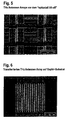
- Fig. 7 shows a further particularly preferred embodiment of a THz antenna array 40 according to the invention in a schematic plan view similar to that in FIG Fig. 4 , Again, the finger structure of the electrodes 41A, 41B is illustrated with the intermediate spacer region 44 extending laterally over at least a portion of the photoconductive region 42.
- the THz antennas 49 of the array 40 are on an undoped silicon substrate 43 according to the Fig. 5 and Fig. 6 explained manufacturing method applied.
- the finger-like electrodes 41A, 41B of the finger structure have in their lateral extent a T-shaped geometry 46 facing away from the photoconductive region, which is used to form a THZ resonator. the square-like region 48 between the electrodes 41A, 41B - contributes.
- THz antenna arrays 20, 30, 40 can furthermore be improved by an employment of nanotechnology, photonics and microsystem methods with respect to an achievable THz output signal power of preferably at least an order of magnitude are, but the production costs are affected only slightly.
- FIG. 9 a schematic representation of the above-described THz antenna arrays 20, 30, 40 - here partially a THz antenna 29, 39, 49, 49 ', 49 "thereof, in a dark optical excitation 51, in particular in the photoconductive region 22, 32, 42, which is already focused according to the improvement between the first electrode 21A, 31A, 41A and the second electrode 21B, 31B, 41B and to a brightly represented THz emission 53 through the THz transparent substrate, not shown, ie
- the further development of a focused optical excitation can be achieved by an arrangement of a microlens not shown in detail on the excitation side of the THz antenna Fig.
- THz antennas for example, as here in the form of a metal-semiconductor-metal arrangement (MSM antenna) on the present case from center to center of adjacent antennas measured length of ⁇ 2 , based on THz wavelength
- MSM antenna metal-semiconductor-metal arrangement
- the directivity of a THz antenna array can be significantly improved.
- Fig. 10 and Fig. 11 First, the device design and, secondly, the optical excitation and, third, an increase in efficiency through functionalization of the semiconductor surface with the aid of metallic nanoparticles. In the present case, these are realized in a further preferred embodiment of a THz antenna array 50 and exploit in an improved manner the potential of the classical field theory for the antenna arrays.
- the directivity of the arrangement of the THz antenna array 50 can be significantly improved, whereby the optical losses in surrounding system can be significantly reduced.
- the directivity also depends on the electromagnetic coupling of the individual antennas 59, which can also be improved by advantageous measures such as refractive index adjustments or the like.
- the increase in the antenna distance D may also mean an increase in inactive intermediate areas, ie an enlargement of the spacing areas 24, 34, 44 as described in the preceding figures.
- the in Fig. 9 The following concept of focusing with the aid of a microlens is described in the US Pat Fig. 10 illustrated embodiment of a THz antenna array 50, a microlens array 55 on the excitation side above a THz antenna 59 in the THz antenna array 50 and the microlens array 55 comprehensive component integrated.
- the microlens array 55 focuses the optical excitation 51 in the form of the optical excitation beam on the periodically arranged antennas 59 of the THz antenna array. In this way it is possible, as in Fig.
- a microlens array provided specifically for the THz antenna array 50 can be designed, which correspond to the required antenna spacing D.
- THz signal generation can, as in the present case in the context of a modification, for example, the semiconductor surface, in the form of a deposited layer, consisting of separate gold nanoparticles reach.
- Metallic as well as other materials with a high dielectric constant in the form of particles with diameters in the range of a few nanometers are used here in addition to an increase in the sensor surface and for influencing the field dynamics of the charge carriers generated by the optical excitation.
- the microlens array 55 can be integrated with the THz antenna array 50 to form a THz-emitting component.
- an arrangement of THz antennas as a finger structure in FIG Fig. 11 schematically and above it in extrapolation representation the nano-scaled, functionalized surface 61.
- such a surface 61 can be achieved as a cost-effective process, eg in the context of a deposition of gold nanoparticles on a SiO 2 surface.
- a cost-effective process eg in the context of a deposition of gold nanoparticles on a SiO 2 surface.
- Fig. 12 shows an AFM image, which illustrates the significant separation of the Au particles, which is particularly suitable, the above-mentioned efficiency-enhancing effects of a THz conversion in an emitter, such as in Fig. 9 or Fig. 10 is shown to evoke.
- a THz antenna array as it is in Fig. 1 to Fig. 8 has been described.
Landscapes
- Variable-Direction Aerials And Aerial Arrays (AREA)
Applications Claiming Priority (2)
| Application Number | Priority Date | Filing Date | Title |
|---|---|---|---|
| DE102006014801A DE102006014801A1 (de) | 2006-03-29 | 2006-03-29 | THz-Antennen-Array, System und Verfahren zur Herstellung eines THz-Antennen-Arrays |
| PCT/EP2007/002790 WO2007112925A1 (de) | 2006-03-29 | 2007-03-29 | Thz-antennen-array, system und verfahren zur herstellung eines thz-antennen-arrays |
Publications (2)
| Publication Number | Publication Date |
|---|---|
| EP1999456A1 EP1999456A1 (de) | 2008-12-10 |
| EP1999456B1 true EP1999456B1 (de) | 2016-07-20 |
Family
ID=38267950
Family Applications (1)
| Application Number | Title | Priority Date | Filing Date |
|---|---|---|---|
| EP07723734.5A Not-in-force EP1999456B1 (de) | 2006-03-29 | 2007-03-29 | Thz-antennen-array, system und verfahren zur herstellung eines thz-antennen-arrays |
Country Status (5)
| Country | Link |
|---|---|
| US (1) | US8581784B2 (enExample) |
| EP (1) | EP1999456B1 (enExample) |
| JP (1) | JP2009531841A (enExample) |
| DE (1) | DE102006014801A1 (enExample) |
| WO (1) | WO2007112925A1 (enExample) |
Families Citing this family (26)
| Publication number | Priority date | Publication date | Assignee | Title |
|---|---|---|---|---|
| DE102008023991A1 (de) * | 2008-05-16 | 2009-12-03 | Forschungszentrum Dresden - Rossendorf E.V. | Skalierbare Terahertz-Antennen, ihre Herstellung und Verwendung |
| DE102008031751B3 (de) * | 2008-07-04 | 2009-08-06 | Batop Gmbh | Photoleitende Antenne zur Abstrahlung oder zum Empfang von Terahertz-Strahlung |
| US8563955B2 (en) | 2009-06-12 | 2013-10-22 | Baden-Wurttemberg Stiftung Ggmbh | Passive terahertz radiation source |
| JP4534027B1 (ja) * | 2010-03-01 | 2010-09-01 | 国立大学法人 岡山大学 | 電磁波波面整形素子及びそれを備えた電磁波イメージング装置、並びに電磁波イメージング方法 |
| US8642964B2 (en) * | 2010-08-31 | 2014-02-04 | The United States of America, as represented by the Secretary of Commerce, NIST | High repetition rate photoconductive terahertz emitter using a radio frequency bias |
| US9935355B2 (en) * | 2010-10-29 | 2018-04-03 | Agency For Science, Technology And Research | THz photomixer emitter and method |
| JP2012222303A (ja) * | 2011-04-13 | 2012-11-12 | Seiko Epson Corp | テラヘルツ波発生装置、カメラ、イメージング装置および計測装置 |
| JP5765086B2 (ja) * | 2011-06-24 | 2015-08-19 | セイコーエプソン株式会社 | テラヘルツ波発生装置、カメラ、イメージング装置および計測装置 |
| WO2013112608A1 (en) * | 2012-01-23 | 2013-08-01 | The Regents Of The University Of Michigan | Photoconductive device with plasmonic electrodes |
| DE102012010926A1 (de) | 2012-06-04 | 2013-12-05 | Amo Gmbh | Bimetall-Halbleiterstruktur zur Erzeugung von gepulsten und kontinuierlichen elektromagnetischen Feldsignalen im Mikrowellen-, Millimeterwellen und Terahertz-Frequenzbereich |
| DE102014100350B4 (de) | 2013-01-15 | 2021-12-02 | Electronics And Telecommunications Research Institute | Photomischer mit photonischem Kristall vom Typ mit großflächiger Anordnung zum Erzeugen und Detektieren von Breitband-Terahertz-Wellen |
| EP3155702B1 (en) * | 2014-06-13 | 2020-12-16 | The Regents of The University of California | Low-duty-cycle continuous-wave photoconductive terahertz imaging and spectroscopy systems |
| US10714838B2 (en) * | 2014-10-30 | 2020-07-14 | Mitsubishi Electric Corporation | Array antenna apparatus and method of manufacturing the same |
| EP3302224B1 (en) | 2015-05-27 | 2020-10-14 | The Regents of The University of California | Terahertz endoscopy through laser-driven terahertz sources and detectors |
| US10436780B2 (en) * | 2015-06-04 | 2019-10-08 | Purdue Research Foundation | Multi-site particle sensing system |
| KR102257556B1 (ko) * | 2016-03-03 | 2021-05-31 | 한국전자통신연구원 | 테라헤르츠파 발생 장치 및 이를 이용한 테라헤르츠 파면 제어 방법 |
| RU2622093C9 (ru) * | 2016-05-13 | 2017-07-25 | Государственное образовательное учреждение высшего профессионального образования Кыргызско-Российский Славянский университет (КРСУ) | Источник терагерцового излучения |
| DE102016116900B3 (de) | 2016-09-09 | 2017-11-16 | Helmholtz-Zentrum Dresden - Rossendorf E.V. | THz-Antenne und Vorrichtung zum Senden und/oder Empfangen von THz-Strahlung |
| DE102016011383A1 (de) | 2016-09-21 | 2018-03-22 | Batop Gmbh | Photoleitende Antenne zur Erzeugung oder zum Empfang von Terahertz-Strahlung |
| CN106486729B (zh) * | 2016-09-29 | 2021-05-04 | 东南大学 | 基于人工表面等离激元的紧凑型闭环谐振器 |
| WO2018195429A1 (en) | 2017-04-20 | 2018-10-25 | The Regents Of The University Of California | Systems and methods for high frequency nanoscopy |
| WO2021067635A1 (en) | 2019-10-01 | 2021-04-08 | The Regents Of The University Of California | Method for identifying chemical and structural variations through terahertz time-domain spectroscopy |
| EP4052458A4 (en) | 2019-10-31 | 2023-11-29 | The Regents of the University of California | METHOD AND SYSTEMS FOR DETECTING WATER STATUS IN PLANTS USING TERAHERTZ RADIATION |
| RU201847U1 (ru) * | 2020-10-21 | 2021-01-15 | Федеральное государственное бюджетное образовательное учреждение высшего образования «Сибирский государственный университет геосистем и технологий» (СГУГиТ) | Фотопроводящая антенная решетка |
| CN112510352A (zh) * | 2020-11-04 | 2021-03-16 | 西南科技大学 | 一种微结构光电导天线太赫兹波辐射方法及系统 |
| WO2022154994A2 (en) | 2020-12-01 | 2022-07-21 | The Regents Of The University Of California | Systems and methods for wavelength conversion through plasmon-coupled surface states |
Citations (2)
| Publication number | Priority date | Publication date | Assignee | Title |
|---|---|---|---|---|
| US5401953A (en) * | 1993-09-23 | 1995-03-28 | The United States Of America As Represented By The Administrator Of The National Aeronautics And Space Administration | Optically-switched submillimeter-wave oscillator and radiator having a switch-to-switch propagation delay |
| US20050215031A1 (en) * | 2004-03-26 | 2005-09-29 | Canon Kabushiki Kaisha | Photo-semiconductor device and method of manufacturing the same |
Family Cites Families (6)
| Publication number | Priority date | Publication date | Assignee | Title |
|---|---|---|---|---|
| US5663639A (en) * | 1994-01-18 | 1997-09-02 | Massachusetts Institute Of Technology | Apparatus and method for optical heterodyne conversion |
| JPWO2003028173A1 (ja) * | 2001-09-21 | 2005-01-13 | 株式会社ニコン | テラヘルツ光装置 |
| GB2392782B (en) * | 2002-09-04 | 2005-07-13 | Teraview Ltd | An Antenna |
| JP4794878B2 (ja) | 2004-03-26 | 2011-10-19 | キヤノン株式会社 | 光伝導素子 |
| JP4546326B2 (ja) * | 2004-07-30 | 2010-09-15 | キヤノン株式会社 | センシング装置 |
| DE102004046123A1 (de) | 2004-09-23 | 2006-08-24 | Forschungszentrum Rossendorf E.V. | Kohärente Terahertz-Strahlungsquelle |
-
2006
- 2006-03-29 DE DE102006014801A patent/DE102006014801A1/de not_active Withdrawn
-
2007
- 2007-03-29 WO PCT/EP2007/002790 patent/WO2007112925A1/de not_active Ceased
- 2007-03-29 JP JP2009501952A patent/JP2009531841A/ja active Pending
- 2007-03-29 US US12/294,442 patent/US8581784B2/en not_active Expired - Fee Related
- 2007-03-29 EP EP07723734.5A patent/EP1999456B1/de not_active Not-in-force
Patent Citations (2)
| Publication number | Priority date | Publication date | Assignee | Title |
|---|---|---|---|---|
| US5401953A (en) * | 1993-09-23 | 1995-03-28 | The United States Of America As Represented By The Administrator Of The National Aeronautics And Space Administration | Optically-switched submillimeter-wave oscillator and radiator having a switch-to-switch propagation delay |
| US20050215031A1 (en) * | 2004-03-26 | 2005-09-29 | Canon Kabushiki Kaisha | Photo-semiconductor device and method of manufacturing the same |
Also Published As
| Publication number | Publication date |
|---|---|
| JP2009531841A (ja) | 2009-09-03 |
| WO2007112925A1 (de) | 2007-10-11 |
| US20110080329A1 (en) | 2011-04-07 |
| US8581784B2 (en) | 2013-11-12 |
| DE102006014801A1 (de) | 2007-10-04 |
| EP1999456A1 (de) | 2008-12-10 |
Similar Documents
| Publication | Publication Date | Title |
|---|---|---|
| EP1999456B1 (de) | Thz-antennen-array, system und verfahren zur herstellung eines thz-antennen-arrays | |
| DE60133365T2 (de) | Photodetektor mit senkrechtem Metall-Halbleiter, Mikroresonator und Herstellungsverfahren | |
| DE60318512T2 (de) | Fotoelektrisches Konversionselement und fotoelektrische Vorrichtung | |
| DE102009037185B4 (de) | Organische Leuchtdiode | |
| DE112014004277T5 (de) | Terahertz-Lichtquellenchip, Lichtquellenvorrichtung, Lichtquellenanordnung und ihr Herstellungsverfahren | |
| EP1399994B1 (de) | Photonen-emitter und datenübertragungsvorrichtung | |
| DE69636016T2 (de) | Verharen zur Herstellung einer Lichtempfangsvorrichtung | |
| DE112008002737B4 (de) | Plasmonische Hochgeschwindigkeitsvorrichtungen zum Verbessern der Leistungsfähigkeit mikroelektronischer Vorrichtungen | |
| DE112010002092T5 (de) | Fotodetektoren | |
| EP3449508B1 (de) | Strahlungsdetektor und verfahren zu dessen herstellung | |
| DE112022002328T5 (de) | Elektrooptischer Modulator und Verfahren zu dessen Bildung | |
| EP1825530B1 (de) | Kohärente terahertz-strahlungsquelle | |
| DE102016014939B4 (de) | Laservorrichtung, basierend auf einem photonischen Kristall mit säulen- oder wandförmigen Halbleiterelementen, und Verfahren zu deren Betrieb und Herstellung | |
| DE112022002796T5 (de) | Wellenleiterelement | |
| DE4329985C2 (de) | Sonde für die optische Nahfeldmikroskopie | |
| DE112022000898T5 (de) | Wellenleiterelement | |
| EP3149778A1 (de) | Plasmonisches bauteil und plasmonischer photodetektor sowie deren herstellungsverfahren | |
| EP2120291A1 (de) | Skalierbare Terahertz-Antennen | |
| DE112022002553B4 (de) | Optische abtastvorrichtung | |
| DE102012010926A1 (de) | Bimetall-Halbleiterstruktur zur Erzeugung von gepulsten und kontinuierlichen elektromagnetischen Feldsignalen im Mikrowellen-, Millimeterwellen und Terahertz-Frequenzbereich | |
| EP4449567A1 (de) | Oberflächenemittierender photonischer-kristall-laser, optoelektronisches system und verfahren zur herstellung eines oberflächenemittierenden photonischer-kristall-lasers | |
| EP3574532B1 (de) | Metall-isolator-graphen diode | |
| DE102015112330B4 (de) | Nanostruktureinrichtung und Verfahren zum Herstellen einer Nanostruktureinrichtung | |
| WO2023232950A1 (de) | Einzelphotonenquelle, wafer und verfahren zur herstellung einer einzelphotonenquelle | |
| DE4421256A1 (de) | Feldeffekt-Mikrotriode |
Legal Events
| Date | Code | Title | Description |
|---|---|---|---|
| PUAI | Public reference made under article 153(3) epc to a published international application that has entered the european phase |
Free format text: ORIGINAL CODE: 0009012 |
|
| 17P | Request for examination filed |
Effective date: 20080918 |
|
| AK | Designated contracting states |
Kind code of ref document: A1 Designated state(s): AT BE BG CH CY CZ DE DK EE ES FI FR GB GR HU IE IS IT LI LT LU LV MC MT NL PL PT RO SE SI SK TR |
|
| 17Q | First examination report despatched |
Effective date: 20090202 |
|
| R17C | First examination report despatched (corrected) |
Effective date: 20090331 |
|
| DAX | Request for extension of the european patent (deleted) | ||
| GRAP | Despatch of communication of intention to grant a patent |
Free format text: ORIGINAL CODE: EPIDOSNIGR1 |
|
| INTG | Intention to grant announced |
Effective date: 20160203 |
|
| GRAS | Grant fee paid |
Free format text: ORIGINAL CODE: EPIDOSNIGR3 |
|
| GRAA | (expected) grant |
Free format text: ORIGINAL CODE: 0009210 |
|
| AK | Designated contracting states |
Kind code of ref document: B1 Designated state(s): AT BE BG CH CY CZ DE DK EE ES FI FR GB GR HU IE IS IT LI LT LU LV MC MT NL PL PT RO SE SI SK TR |
|
| REG | Reference to a national code |
Ref country code: GB Ref legal event code: FG4D Free format text: NOT ENGLISH |
|
| REG | Reference to a national code |
Ref country code: CH Ref legal event code: EP |
|
| REG | Reference to a national code |
Ref country code: IE Ref legal event code: FG4D Free format text: LANGUAGE OF EP DOCUMENT: GERMAN |
|
| REG | Reference to a national code |
Ref country code: AT Ref legal event code: REF Ref document number: 814489 Country of ref document: AT Kind code of ref document: T Effective date: 20160815 |
|
| REG | Reference to a national code |
Ref country code: DE Ref legal event code: R096 Ref document number: 502007014953 Country of ref document: DE |
|
| REG | Reference to a national code |
Ref country code: LT Ref legal event code: MG4D |
|
| REG | Reference to a national code |
Ref country code: NL Ref legal event code: MP Effective date: 20160720 |
|
| PG25 | Lapsed in a contracting state [announced via postgrant information from national office to epo] |
Ref country code: NL Free format text: LAPSE BECAUSE OF FAILURE TO SUBMIT A TRANSLATION OF THE DESCRIPTION OR TO PAY THE FEE WITHIN THE PRESCRIBED TIME-LIMIT Effective date: 20160720 Ref country code: LT Free format text: LAPSE BECAUSE OF FAILURE TO SUBMIT A TRANSLATION OF THE DESCRIPTION OR TO PAY THE FEE WITHIN THE PRESCRIBED TIME-LIMIT Effective date: 20160720 Ref country code: FI Free format text: LAPSE BECAUSE OF FAILURE TO SUBMIT A TRANSLATION OF THE DESCRIPTION OR TO PAY THE FEE WITHIN THE PRESCRIBED TIME-LIMIT Effective date: 20160720 Ref country code: IS Free format text: LAPSE BECAUSE OF FAILURE TO SUBMIT A TRANSLATION OF THE DESCRIPTION OR TO PAY THE FEE WITHIN THE PRESCRIBED TIME-LIMIT Effective date: 20161120 Ref country code: IT Free format text: LAPSE BECAUSE OF FAILURE TO SUBMIT A TRANSLATION OF THE DESCRIPTION OR TO PAY THE FEE WITHIN THE PRESCRIBED TIME-LIMIT Effective date: 20160720 |
|
| PG25 | Lapsed in a contracting state [announced via postgrant information from national office to epo] |
Ref country code: PL Free format text: LAPSE BECAUSE OF FAILURE TO SUBMIT A TRANSLATION OF THE DESCRIPTION OR TO PAY THE FEE WITHIN THE PRESCRIBED TIME-LIMIT Effective date: 20160720 Ref country code: ES Free format text: LAPSE BECAUSE OF FAILURE TO SUBMIT A TRANSLATION OF THE DESCRIPTION OR TO PAY THE FEE WITHIN THE PRESCRIBED TIME-LIMIT Effective date: 20160720 Ref country code: SE Free format text: LAPSE BECAUSE OF FAILURE TO SUBMIT A TRANSLATION OF THE DESCRIPTION OR TO PAY THE FEE WITHIN THE PRESCRIBED TIME-LIMIT Effective date: 20160720 Ref country code: PT Free format text: LAPSE BECAUSE OF FAILURE TO SUBMIT A TRANSLATION OF THE DESCRIPTION OR TO PAY THE FEE WITHIN THE PRESCRIBED TIME-LIMIT Effective date: 20161121 Ref country code: GR Free format text: LAPSE BECAUSE OF FAILURE TO SUBMIT A TRANSLATION OF THE DESCRIPTION OR TO PAY THE FEE WITHIN THE PRESCRIBED TIME-LIMIT Effective date: 20161021 Ref country code: LV Free format text: LAPSE BECAUSE OF FAILURE TO SUBMIT A TRANSLATION OF THE DESCRIPTION OR TO PAY THE FEE WITHIN THE PRESCRIBED TIME-LIMIT Effective date: 20160720 |
|
| REG | Reference to a national code |
Ref country code: DE Ref legal event code: R097 Ref document number: 502007014953 Country of ref document: DE |
|
| PG25 | Lapsed in a contracting state [announced via postgrant information from national office to epo] |
Ref country code: RO Free format text: LAPSE BECAUSE OF FAILURE TO SUBMIT A TRANSLATION OF THE DESCRIPTION OR TO PAY THE FEE WITHIN THE PRESCRIBED TIME-LIMIT Effective date: 20160720 Ref country code: EE Free format text: LAPSE BECAUSE OF FAILURE TO SUBMIT A TRANSLATION OF THE DESCRIPTION OR TO PAY THE FEE WITHIN THE PRESCRIBED TIME-LIMIT Effective date: 20160720 |
|
| PLBE | No opposition filed within time limit |
Free format text: ORIGINAL CODE: 0009261 |
|
| STAA | Information on the status of an ep patent application or granted ep patent |
Free format text: STATUS: NO OPPOSITION FILED WITHIN TIME LIMIT |
|
| PG25 | Lapsed in a contracting state [announced via postgrant information from national office to epo] |
Ref country code: BG Free format text: LAPSE BECAUSE OF FAILURE TO SUBMIT A TRANSLATION OF THE DESCRIPTION OR TO PAY THE FEE WITHIN THE PRESCRIBED TIME-LIMIT Effective date: 20161020 Ref country code: DK Free format text: LAPSE BECAUSE OF FAILURE TO SUBMIT A TRANSLATION OF THE DESCRIPTION OR TO PAY THE FEE WITHIN THE PRESCRIBED TIME-LIMIT Effective date: 20160720 Ref country code: CZ Free format text: LAPSE BECAUSE OF FAILURE TO SUBMIT A TRANSLATION OF THE DESCRIPTION OR TO PAY THE FEE WITHIN THE PRESCRIBED TIME-LIMIT Effective date: 20160720 Ref country code: SK Free format text: LAPSE BECAUSE OF FAILURE TO SUBMIT A TRANSLATION OF THE DESCRIPTION OR TO PAY THE FEE WITHIN THE PRESCRIBED TIME-LIMIT Effective date: 20160720 |
|
| 26N | No opposition filed |
Effective date: 20170421 |
|
| PG25 | Lapsed in a contracting state [announced via postgrant information from national office to epo] |
Ref country code: SI Free format text: LAPSE BECAUSE OF FAILURE TO SUBMIT A TRANSLATION OF THE DESCRIPTION OR TO PAY THE FEE WITHIN THE PRESCRIBED TIME-LIMIT Effective date: 20160720 |
|
| REG | Reference to a national code |
Ref country code: DE Ref legal event code: R119 Ref document number: 502007014953 Country of ref document: DE |
|
| REG | Reference to a national code |
Ref country code: CH Ref legal event code: PL |
|
| GBPC | Gb: european patent ceased through non-payment of renewal fee |
Effective date: 20170329 |
|
| PG25 | Lapsed in a contracting state [announced via postgrant information from national office to epo] |
Ref country code: MC Free format text: LAPSE BECAUSE OF FAILURE TO SUBMIT A TRANSLATION OF THE DESCRIPTION OR TO PAY THE FEE WITHIN THE PRESCRIBED TIME-LIMIT Effective date: 20160720 |
|
| REG | Reference to a national code |
Ref country code: IE Ref legal event code: MM4A |
|
| REG | Reference to a national code |
Ref country code: FR Ref legal event code: ST Effective date: 20171130 |
|
| PG25 | Lapsed in a contracting state [announced via postgrant information from national office to epo] |
Ref country code: FR Free format text: LAPSE BECAUSE OF NON-PAYMENT OF DUE FEES Effective date: 20170331 Ref country code: LU Free format text: LAPSE BECAUSE OF NON-PAYMENT OF DUE FEES Effective date: 20170329 Ref country code: DE Free format text: LAPSE BECAUSE OF NON-PAYMENT OF DUE FEES Effective date: 20171003 |
|
| PG25 | Lapsed in a contracting state [announced via postgrant information from national office to epo] |
Ref country code: GB Free format text: LAPSE BECAUSE OF NON-PAYMENT OF DUE FEES Effective date: 20170329 Ref country code: LI Free format text: LAPSE BECAUSE OF NON-PAYMENT OF DUE FEES Effective date: 20170331 Ref country code: CH Free format text: LAPSE BECAUSE OF NON-PAYMENT OF DUE FEES Effective date: 20170331 Ref country code: IE Free format text: LAPSE BECAUSE OF NON-PAYMENT OF DUE FEES Effective date: 20170329 |
|
| REG | Reference to a national code |
Ref country code: BE Ref legal event code: MM Effective date: 20170331 |
|
| REG | Reference to a national code |
Ref country code: AT Ref legal event code: MM01 Ref document number: 814489 Country of ref document: AT Kind code of ref document: T Effective date: 20170329 |
|
| PG25 | Lapsed in a contracting state [announced via postgrant information from national office to epo] |
Ref country code: BE Free format text: LAPSE BECAUSE OF NON-PAYMENT OF DUE FEES Effective date: 20170331 |
|
| PG25 | Lapsed in a contracting state [announced via postgrant information from national office to epo] |
Ref country code: AT Free format text: LAPSE BECAUSE OF NON-PAYMENT OF DUE FEES Effective date: 20170329 |
|
| PG25 | Lapsed in a contracting state [announced via postgrant information from national office to epo] |
Ref country code: MT Free format text: LAPSE BECAUSE OF FAILURE TO SUBMIT A TRANSLATION OF THE DESCRIPTION OR TO PAY THE FEE WITHIN THE PRESCRIBED TIME-LIMIT Effective date: 20160720 |
|
| PG25 | Lapsed in a contracting state [announced via postgrant information from national office to epo] |
Ref country code: HU Free format text: LAPSE BECAUSE OF FAILURE TO SUBMIT A TRANSLATION OF THE DESCRIPTION OR TO PAY THE FEE WITHIN THE PRESCRIBED TIME-LIMIT; INVALID AB INITIO Effective date: 20070329 |
|
| PG25 | Lapsed in a contracting state [announced via postgrant information from national office to epo] |
Ref country code: CY Free format text: LAPSE BECAUSE OF NON-PAYMENT OF DUE FEES Effective date: 20160720 |
|
| PG25 | Lapsed in a contracting state [announced via postgrant information from national office to epo] |
Ref country code: TR Free format text: LAPSE BECAUSE OF FAILURE TO SUBMIT A TRANSLATION OF THE DESCRIPTION OR TO PAY THE FEE WITHIN THE PRESCRIBED TIME-LIMIT Effective date: 20160720 |