EP1998370A2 - Electronic assembly comprising solderable thermal interface and methods of manufacture - Google Patents
Electronic assembly comprising solderable thermal interface and methods of manufacture Download PDFInfo
- Publication number
- EP1998370A2 EP1998370A2 EP08016462A EP08016462A EP1998370A2 EP 1998370 A2 EP1998370 A2 EP 1998370A2 EP 08016462 A EP08016462 A EP 08016462A EP 08016462 A EP08016462 A EP 08016462A EP 1998370 A2 EP1998370 A2 EP 1998370A2
- Authority
- EP
- European Patent Office
- Prior art keywords
- solder
- layer
- die
- recited
- lid
- Prior art date
- Legal status (The legal status is an assumption and is not a legal conclusion. Google has not performed a legal analysis and makes no representation as to the accuracy of the status listed.)
- Withdrawn
Links
Images


Classifications
-
- H—ELECTRICITY
- H10—SEMICONDUCTOR DEVICES; ELECTRIC SOLID-STATE DEVICES NOT OTHERWISE PROVIDED FOR
- H10W—GENERIC PACKAGES, INTERCONNECTIONS, CONNECTORS OR OTHER CONSTRUCTIONAL DETAILS OF DEVICES COVERED BY CLASS H10
- H10W72/00—Interconnections or connectors in packages
- H10W72/30—Die-attach connectors
-
- H—ELECTRICITY
- H10—SEMICONDUCTOR DEVICES; ELECTRIC SOLID-STATE DEVICES NOT OTHERWISE PROVIDED FOR
- H10W—GENERIC PACKAGES, INTERCONNECTIONS, CONNECTORS OR OTHER CONSTRUCTIONAL DETAILS OF DEVICES COVERED BY CLASS H10
- H10W40/00—Arrangements for thermal protection or thermal control
- H10W40/70—Fillings or auxiliary members in containers or in encapsulations for thermal protection or control
-
- H—ELECTRICITY
- H10—SEMICONDUCTOR DEVICES; ELECTRIC SOLID-STATE DEVICES NOT OTHERWISE PROVIDED FOR
- H10W—GENERIC PACKAGES, INTERCONNECTIONS, CONNECTORS OR OTHER CONSTRUCTIONAL DETAILS OF DEVICES COVERED BY CLASS H10
- H10W40/00—Arrangements for thermal protection or thermal control
- H10W40/70—Fillings or auxiliary members in containers or in encapsulations for thermal protection or control
- H10W40/77—Auxiliary members characterised by their shape
-
- H—ELECTRICITY
- H10—SEMICONDUCTOR DEVICES; ELECTRIC SOLID-STATE DEVICES NOT OTHERWISE PROVIDED FOR
- H10W—GENERIC PACKAGES, INTERCONNECTIONS, CONNECTORS OR OTHER CONSTRUCTIONAL DETAILS OF DEVICES COVERED BY CLASS H10
- H10W72/00—Interconnections or connectors in packages
- H10W72/851—Dispositions of multiple connectors or interconnections
- H10W72/874—On different surfaces
- H10W72/877—Bump connectors and die-attach connectors
-
- H—ELECTRICITY
- H10—SEMICONDUCTOR DEVICES; ELECTRIC SOLID-STATE DEVICES NOT OTHERWISE PROVIDED FOR
- H10W—GENERIC PACKAGES, INTERCONNECTIONS, CONNECTORS OR OTHER CONSTRUCTIONAL DETAILS OF DEVICES COVERED BY CLASS H10
- H10W74/00—Encapsulations, e.g. protective coatings
- H10W74/10—Encapsulations, e.g. protective coatings characterised by their shape or disposition
- H10W74/15—Encapsulations, e.g. protective coatings characterised by their shape or disposition on active surfaces of flip-chip devices, e.g. underfills
-
- H—ELECTRICITY
- H10—SEMICONDUCTOR DEVICES; ELECTRIC SOLID-STATE DEVICES NOT OTHERWISE PROVIDED FOR
- H10W—GENERIC PACKAGES, INTERCONNECTIONS, CONNECTORS OR OTHER CONSTRUCTIONAL DETAILS OF DEVICES COVERED BY CLASS H10
- H10W90/00—Package configurations
- H10W90/701—Package configurations characterised by the relative positions of pads or connectors relative to package parts
- H10W90/721—Package configurations characterised by the relative positions of pads or connectors relative to package parts of bump connectors
- H10W90/724—Package configurations characterised by the relative positions of pads or connectors relative to package parts of bump connectors between a chip and a stacked insulating package substrate, interposer or RDL
-
- H—ELECTRICITY
- H10—SEMICONDUCTOR DEVICES; ELECTRIC SOLID-STATE DEVICES NOT OTHERWISE PROVIDED FOR
- H10W—GENERIC PACKAGES, INTERCONNECTIONS, CONNECTORS OR OTHER CONSTRUCTIONAL DETAILS OF DEVICES COVERED BY CLASS H10
- H10W90/00—Package configurations
- H10W90/701—Package configurations characterised by the relative positions of pads or connectors relative to package parts
- H10W90/731—Package configurations characterised by the relative positions of pads or connectors relative to package parts of die-attach connectors
- H10W90/734—Package configurations characterised by the relative positions of pads or connectors relative to package parts of die-attach connectors between a chip and a stacked insulating package substrate, interposer or RDL
-
- H—ELECTRICITY
- H10—SEMICONDUCTOR DEVICES; ELECTRIC SOLID-STATE DEVICES NOT OTHERWISE PROVIDED FOR
- H10W—GENERIC PACKAGES, INTERCONNECTIONS, CONNECTORS OR OTHER CONSTRUCTIONAL DETAILS OF DEVICES COVERED BY CLASS H10
- H10W90/00—Package configurations
- H10W90/701—Package configurations characterised by the relative positions of pads or connectors relative to package parts
- H10W90/731—Package configurations characterised by the relative positions of pads or connectors relative to package parts of die-attach connectors
- H10W90/736—Package configurations characterised by the relative positions of pads or connectors relative to package parts of die-attach connectors between a chip and a stacked lead frame, conducting package substrate or heat sink
Definitions
- the present invention relates generally to electronics packaging. More particularly, the present invention relates to an electronic assembly that includes an integrated circuit package comprising a solderable thermal interface between the integrated circuit and a heat spreader to dissipate heat generated in a high speed integrated circuit, and to manufacturing methods related thereto.
- Integrated circuits are typically assembled into packages by physically and electrically coupling them to a substrate made of organic or ceramic material.
- One or more IC packages can be physically and electrically coupled to a printed circuit board (PCB) to form an "electronic assembly".
- the "electronic assembly” can be part of an “electronic system”.
- An “electronic system” is broadly defined herein as any product comprising an “electronic assembly”.
- Examples of electronic systems include computers (e.g., desktop, laptop, handheld, server, etc.), wireless communications devices (e.g., cellular phones, cordless phones, pagers, etc.), computerrelated peripherals (e.g., printers, scanners, monitors, etc.), entertainment devices (e.g., televisions, radios, stereos, tape and compact disc players, video cassette recorders, MP3 (Motion Picture Experts Group, Audio Layer 3) players, etc.), and the like.
- computers e.g., desktop, laptop, handheld, server, etc.
- wireless communications devices e.g., cellular phones, cordless phones, pagers, etc.
- computerrelated peripherals e.g., printers, scanners, monitors, etc.
- entertainment devices e.g., televisions, radios, stereos, tape and compact disc players, video cassette recorders, MP3 (Motion Picture Experts Group, Audio Layer 3) players, etc.
- An IC substrate may comprise a number of metal layers selectively patterned to provide metal interconnect lines (referred to herein as "traces"), and one or more electronic components mounted on one or more surfaces of the substrate.
- the electronic component or components are functionally connected to other elements of an electronic system through a hierarchy of electrically conductive paths that include the substrate traces.
- the substrate traces typically carry signals that are transmitted between the electronic components, such as ICs, of the system.
- Some ICs have a relatively large number of input/output (I/O) terminals, as well as a large number of power and ground terminals.
- C4 controlled collapse chip connect
- US-A-6 091 603 (DAVES GLENN G ET AL) 18 July 2000 (2000-07-18) discloses an integrated circuit package having a chip, a thermally conductive compliant material, a heat spreader, an understructure, and a lid.
- A. AMENDOLA,C.A. PECK AND C. PRASAD "COOLING STRUCTURE FOR AN INTEGRATED CIRCUIT MODULE" IBM TECHNICAL DISCLOSURE BULLETIN., vol 23, no. 2, July 1980 (1980-07), page 602, XP002191051 IBM CORP, NEW YORK., US ISSN: 0018-8689 discloses mounting a ceramic cap over a semiconductor device, using solder. A metallised area of the cap is provided over the device, and the solder is reflowed between the device and the metallised area of the cap.
- R.C.MILLER "Structure for achieving thermal enhancement in a semiconductor package" IBM TECHNICAL DISCLOSURE BULLETIN., vol. 23, no. 6 November 1980 (1980-11), page 2308, XP002191052 IBM CORP. NEW YORK., US ISSN: 0018-8689 discloses mounting a cap, having a metallization layer, on a device using solder.
- PATENT ABSTRACTS OF JAPAN vol, 015, no365 (E-1111), 13 September 1991 (1991-09-13 )-& JP 03 142860 A (HITACHI LTD), 18 June 1991 (1991-06-18) discloses mounting a cap over a semiconductor chip using solder.
- the invention provides an assembly as defined in claim 1, an integrated circuit package as defined in Claim 8, an assembly as defined in Claim 20, and methods as defined in Claims 23 and 27.
- the present invention provides a solution to thermal dissipation problems that are associated with prior art packaging of integrated circuits that operate at high clock speeds and high power levels by employing a highly conductive solder material as a thermal interface between an IC die and a heat spreader.
- a highly conductive solder material as a thermal interface between an IC die and a heat spreader.
- an IC die is mounted to an organic land grid array (OLGA) substrate using C4 technology.
- An integrated heat spreader is attached to the back surface of the die using a highly conductive solderable thermal interface material after suitable preparation of the die and heat spreader surfaces.
- a solderable thermal interface material is selected that has a relatively low melting point, in order to minimize thermal stresses in the package that can be generated, because the silicon die has a relatively low thermal coefficient of expansion (TCE) compared to the TCE of the OLGA substrate. By reducing thermal stresses, the package is less likely to experience warpage when it is subjected to heat, for example during solder reflow.
- the solderable thermal interface material also has excellent thermal conductive properties.
- the integrated heat spreader can also be coupled to the OLGA substrate around the die periphery with a suitable sealant in order to provide mechanical strength.
- a low melting point solder as a thermal interface material avoids many problems associated with the use of polymeric thermal interface materials (e.g. those containing silver or aluminum), such as resin separation, out-gassing, delamination, pump-out, and so forth.
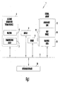
- FIG. 1 is a block diagram of an electronic system 1 incorporating at least one electronic assembly 4 with a solderable thermal interface in accordance with one embodiment of the invention.
- Electronic system 1 is merely one example of an electronic system in which the present invention can be used.
- electronic system 1 comprises a data processing system that includes a system bus 2 to couple the various components of the system.
- System bus 2 provides communications links among the various components of the electronic system 1 and can be implemented as a single bus, as a combination of busses, or in any other suitable manner.
- Electronic assembly 4 is coupled to system bus 2.
- Electronic assembly 4 can include any circuit or combination of circuits.
- electronic assembly 4 includes a processor 6 which can be of any type.
- processor means any type of computational circuit, such as but not limited to a microprocessor, a microcontroller, a complex instruction set computing (CISC) microprocessor, a reduced instruction set computing (RISC) microprocessor, a very long instruction word (VLIW) microprocessor, a graphics processor, a digital signal processor (DSP), or any other type of processor or processing circuit.
- CISC complex instruction set computing
- RISC reduced instruction set computing
- VLIW very long instruction word
- DSP digital signal processor
- circuits that can be included in electronic assembly 4 are a custom circuit, an application-specific integrated circuit (ASIC), or the like, such as, for example, one or more circuits (such as a communications circuit 7) for use in wireless devices like cellular telephones, pagers, portable computers, two-way radios, and similar electronic systems.
- ASIC application-specific integrated circuit
- the IC can perform any other type of function.
- Electronic system 1 can also include an external memory 10, which in turn can include one or more memory elements suitable to the particular application, such as a main memory 12 in the form of random access memory (RAM), one or more hard drives 14, and/or one or more drives that handle removable media 16 such as floppy diskettes, compact disks (CDs), digital video disk (DVD), and the like.
- a main memory 12 in the form of random access memory (RAM)
- RAM random access memory
- hard drives 14 and/or one or more drives that handle removable media 16 such as floppy diskettes, compact disks (CDs), digital video disk (DVD), and the like.
- removable media 16 such as floppy diskettes, compact disks (CDs), digital video disk (DVD), and the like.
- Electronic system 1 can also include a display device 8, a speaker 9, and a keyboard and/or controller 20, which can include a mouse, trackball, game controller, voice-recognition device, or any other device that permits a system user to input information into and receive information from the electronic system 1.
- a display device 8 a speaker 9
- a keyboard and/or controller 20 which can include a mouse, trackball, game controller, voice-recognition device, or any other device that permits a system user to input information into and receive information from the electronic system 1.
- FIG. 2 illustrates a cross-sectional representation of an integrated circuit (IC) package, in accordance with one embodiment of the invention.
- the IC package comprises a die 50 mounted on an organic land grid array (OLGA) substrate 54, and a lid or integrated head spreader (IHS) 52. While an OLGA substrate is shown, the present invention is not limited to use with an OLGA substrate, and any other type of substrate can be employed
- the IC package illustrated in FIG. 2 can form part of electronic assembly 4 shown in FIG. 1 .
- Die 50 can be of any type. In one embodiment, die 50 is a processor.
- die 50 comprises a plurality of signal conductors (not shown) that terminate in pads on the bottom surface of die 50 (not shown). These pads can be coupled to corresponding lands 68 representing signal, power, or ground nodes on OLGA substrate 54 by appropriate connections such as C4 solder bumps 66.
- a suitable underfill 62 such as an epoxy material, can be used to surround C4 solder bumps 66 to provide mechanical stability and strength.
- lid or IHS 52 forms a cover over die 50.
- IHS 52 is thermally coupled to a surface of die 50 through a suitable solderable thermal interface 60.
- Die 50 can thus dissipate a substantial amount of heat through thermal interface 60 to IHS 52.
- the solderable thermal interface 60 comprises a material that is capable of conducting heat at a relatively high rate, and that has a relatively low melting point to minimize thermal stresses in the package when it is subjected to heat, for example during solder reflow.
- IHS 52 can be mechanically supported by coupling its wall or support member 53 to the surface of OLGA substrate 54 through a suitable sealant 64.
- the wall or support member 53 is located at the periphery of IHS 52.
- IHS 52 can extend beyond the support member 53.
- a heat spreader of any shape can be formed as part of or attached to IHS 52, in order to increase the rate of heat dissipation from die 50.
- OLGA substrate 54 can be of any type, including a multi-layer substrate. OLGA substrate 54 can be mounted to an additional substrate 70, such as a printed circuit board (PCB) or card. OLGA substrate 54 can comprise, for example, a plurality of lands 57 that can be mechanically and electrically coupled to corresponding lands 59 of substrate 70 by suitable connectors such as ball grid array (BGA) solder balls 58.
- PCB printed circuit board
- BGA ball grid array
- BGA arrangement 56 is illustrated in FIG. 2 for coupling OLGA substrate 54 to substrate 70
- the present invention is not limited to use with a BGA arrangement, and it can be used with any other type of packaging technology, e.g. land grid array (LGA), chip scale package (CSP), or the like.
- LGA land grid array
- CSP chip scale package
- the present invention is not to be construed as limited to use in C4 packages, and it can be used with any other type of IC package where the herein-described features of the present invention provide an advantage.
- FIG. 3 illustrates a cross-sectional representation of a thermal interface (also referred to herein as a thermally conductive element) 60 between a die 50 and a lid or integrated heat spreader (IHS) 52, in accordance with one embodiment of the invention.
- a thermal interface also referred to herein as a thermally conductive element
- IHS integrated heat spreader
- one or more metal layers 82, 84, and 86 are deposited on the die surface that is to be coupled via thermal interface 60 to the IHS 52.
- the wafer surface can be prepared with a sputter etch, if desired, to improve the adhesion of the adhesion layer 82 to the die surface; however, a sputter etch is not essential. Nor is the condition of the wafer surface essential.
- the wafer surface can be in unpolished, polished, or back-ground form.
- a 500 Angstrom layer of titanium is sputtered onto the etched surface. Chromium (Cr), vanadium (V), and possibly zirconium (Zr) could be substituted for Ti.
- a second metal layer 84 such as nickel-vanadium (NiV), is deposited.
- a 3500 Angstrom layer of NiV is sputtered onto the Ti layer.
- a purpose of layer 84 is to serve as a diffusion barrier to prevent any reaction of solder in the thermal interface 60 with the adhesion layer 82, which could result in possible delamination of the thermal interface 60 from the die 50.
- Layer 84 is not necessarily required, depending upon the composition of the adhesion layer 82, the solder material in the thermal interface 60, and the thermal treatment during the reflow operation.
- a third metal layer 86 such as gold (Au) is deposited.
- Au gold
- a 600 Angstrom layer of Au is sputtered onto the NiV layer. Any metal that "wets" the chosen solder material in the thermal interface 60 could be substituted for gold. Nickel is one example.
- IHS 52 comprises copper (Cu); in another embodiment IHS 52 comprises aluminum-silicon-carbide (AlSiC).
- AlSiC aluminum-silicon-carbide
- a 2-5 micron thick layer 88 ofNi is deposited on the lower surface of IHS 52.
- Electroless Ni plating is carried out in a Niklad 767 bath using a medium force solution. Any metal that "wets" the chosen solder material in the thermal interface 60 could be substituted for nickel. Gold is one example. A combination of metals or alloys could also be substituted for the single layer 88 shown in FIG. 3 .
- solder for a suitable solder material, any of the solder alloys, or a combination thereof, listed in Table 1 would be effective. All are commercially available from Indium Corporation of America, Utica, NY under the corresponding Indalloy( No.
- the solder can be integrated with a no-clean flux vehicle to form a solder paste with an 89% loading of the selected solder alloy.
- Table 1 Composition Liquidus ((C) Solidus ((C) Thermal Conductivity Watts/Meter (C Indalloy No.
- solder paste is first applied to the back side of the die.
- the solder paste could be applied to the surface of IHS 52 that faces the back side of the die.
- a suitable sealant 64, FIG. 2
- an appropriate force can be applied, for example using a spring, to hold IHS 52 in position.
- the package is then put into a suitable heating environment, such as a flow furnace, for solder reflow.
- the maximum zone temperature in the furnace is maintained at liquidus of the solder material + 30(C, and the time above liquidus is approximately 60 seconds.
- the sealant at the IHS boundary is cured in a conventional oven.
- Any suitable method, or combination of different methods, for depositing the metal layers can be used, such as sputtering, vapor, electrical, screening, stenciling, chemical including chemical vapor deposition (CVD), vacuum, and so forth.
- CVD chemical vapor deposition
- the particular implementation of the IC package is very flexible in terms of the orientation, size, number, and composition of its constituent elements.
- Various embodiments of the invention can be implemented using various combinations of substrate technology, IHS technology, thermal interface material, and sealant to achieve the advantages of the present invention.
- the structure, including types of materials used, dimensions, layout, geometry, and so forth, of the IC package can be built in a wide variety of embodiments, depending upon the requirements of the electronic assembly of which it forms a part.
- FIGS. 2 and 3 are merely representational and are not drawn to scale. Certain proportions thereof may be exaggerated, while others may be minimized. FIGS. 2 and 3 are intended to illustrate various implementations of the invention that can be understood and appropriately carried out by those of ordinary skill in the art.
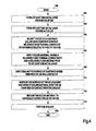
- FIG. 4 is a flow diagram of a method of packaging a die, in accordance with one embodiment of the invention. The method begins at 100.
- At least one metal layer is formed on a surface of a die.
- individual layers of titanium, nickel-vanadium, and gold are successively deposited on the upper surface of die 50 ( FIG. 3 ).
- One or more alloys of these metals could also be used.
- At least one metal layer is formed on a surface of the lid.
- a layer of nickel is deposited on the lower surface of lid or IHS 52 ( FIG. 3 ).
- the die is mounted on a substrate.
- the substrate is an organic substrate
- the die is C4 mounted using a land grid array (LGA) arrangement.
- LGA land grid array
- substrates comprising one or more organic materials, such as epoxies, acrylates, polyimides, polyurethanes, polysulfides, resin-glass weave (e.g. FR-4), nylons, and other similar materials, have a relatively high thermal coefficient of expansion compared with that of the die.
- solder material having a relatively high thermal conductivity and a relatively low melting point is applied to the at least one metal layer of the die.
- a solder material having a relatively low melting point is desirable to employ a solder material having a relatively low melting point to minimize warpage problems when the package is subjected to heat.
- the solder material is any of those listed in Table 1; however, other solder materials besides those listed in Table 1 could be used, provided that they have the qualities previously mentioned.
- the solder material could be applied to the at least one metal layer on the surface of the lid. The solder material can be applied at any suitable stage in the fabrication process.
- a suitable sealant is applied to the surface of the substrate where the support member 53 ( FIG. 2 ) of IHS 52 will contact it
- the IHS is placed and aligned so that the inner surface of the IHS contacts the layer of solder material and, concurrently, the support member 53 of IHS 52 contacts the sealant.
- a spring (not shown) is also placed to secure the assembly with respect to an assembly carrier (not shown).
- the solder material is melted or reflowed by heating so that, when it has cooled, the IHS 52 is physically and thermally coupled to the upper surface of the top metal layer 86 ( FIG. 3 ) on die 50.
- the sealant is cured, for example, by heating, to provide mechanical coupling of the assembly.
- Post cure the securing spring is removed from the assembly carrier. The method ends in 120.
- the present invention provides for an electronic assembly and methods of manufacture thereof that minimize thermal dissipation problems associated with high power delivery.
- An electronic system and/or data processing system that incorporates one or more electronic assemblies that utilize the present invention can handle the relatively high power densities associated with high performance integrated circuits, and such systems are therefore more commercially attractive.
- the present invention can be implemented in a number of different embodiments, including an assembly for a die, an integrated circuit package, an electronic assembly, an electronic system, a data processing system, and a method for packaging an integrated circuit.
- Other embodiments will be readily apparent to those of ordinary skill in the art.
- the elements, materials, geometries, dimensions, and sequence of operations can all be varied to suit particular packaging requirements.
Landscapes
- Cooling Or The Like Of Semiconductors Or Solid State Devices (AREA)
- Wire Bonding (AREA)
Abstract
Description
- The present invention relates generally to electronics packaging. More particularly, the present invention relates to an electronic assembly that includes an integrated circuit package comprising a solderable thermal interface between the integrated circuit and a heat spreader to dissipate heat generated in a high speed integrated circuit, and to manufacturing methods related thereto.
- Integrated circuits (ICs) are typically assembled into packages by physically and electrically coupling them to a substrate made of organic or ceramic material. One or more IC packages can be physically and electrically coupled to a printed circuit board (PCB) to form an "electronic assembly". The "electronic assembly" can be part of an "electronic system". An "electronic system" is broadly defined herein as any product comprising an "electronic assembly". Examples of electronic systems include computers (e.g., desktop, laptop, handheld, server, etc.), wireless communications devices (e.g., cellular phones, cordless phones, pagers, etc.), computerrelated peripherals (e.g., printers, scanners, monitors, etc.), entertainment devices (e.g., televisions, radios, stereos, tape and compact disc players, video cassette recorders, MP3 (Motion Picture Experts Group, Audio Layer 3) players, etc.), and the like.
- In the field of electronic systems there is an incessant competitive pressure among manufacturers to drive the performance of their equipment up while driving down production costs. This is particularly true regarding the packaging of ICs on substrates, where each new generation of packaging must provide increased performance while generally being smaller or more compact in size. As the power demands of high performance IC processors approach and even exceed 100 watts per chip, with localized power densities exceeding 200 watts/square centimeter, the heat dissipating capability of the IC package must correspondingly increase.
- An IC substrate may comprise a number of metal layers selectively patterned to provide metal interconnect lines (referred to herein as "traces"), and one or more electronic components mounted on one or more surfaces of the substrate. The electronic component or components are functionally connected to other elements of an electronic system through a hierarchy of electrically conductive paths that include the substrate traces. The substrate traces typically carry signals that are transmitted between the electronic components, such as ICs, of the system. Some ICs have a relatively large number of input/output (I/O) terminals, as well as a large number of power and ground terminals.
- One of the conventional methods for mounting an IC on a substrate is called "controlled collapse chip connect" (C4). In fabricating a C4 package, the electrically conductive terminations or lands (generally referred to as "electrical contacts") of an IC component are soldered directly to corresponding lands on the surface of the substrate using reflowable solder bumps or balls. The C4 process is widely used because of its robustness and simplicity.
- As the internal circuitry of ICs, such as processors, operates at higher and higher clock frequencies, and as ICs operate at higher and higher power levels, the amount of heat generated by such IC's can increase to unacceptable levels.
- For the reasons stated above, and for other reasons stated below which will become apparent to those skilled in the art upon reading and understanding the present specification, there is a significant need in the art for a method and apparatus for packaging an IC on a substrate that minimizes heat dissipation problems associated with high clock frequencies and high power densities.
-
US-A-6 091 603 (DAVES GLENN G ET AL) 18 July 2000 (2000-07-18) discloses an integrated circuit package having a chip, a thermally conductive compliant material, a heat spreader, an understructure, and a lid. -
US-A-4 561 011 (KOHARA MASANOBU ET AL ) 24 December 19985 (1985-12-24) discloses adhering a metal plate to a die and positioning a heat sink close to the metal plate, leaving an air gap between the metal plate and the heat sink. - A. AMENDOLA,C.A. PECK AND C. PRASAD: "COOLING STRUCTURE FOR AN INTEGRATED CIRCUIT MODULE" IBM TECHNICAL DISCLOSURE BULLETIN., vol 23, no. 2, July 1980 (1980-07), page 602, XP002191051 IBM CORP, NEW YORK., US ISSN: 0018-8689 discloses mounting a ceramic cap over a semiconductor device, using solder. A metallised area of the cap is provided over the device, and the solder is reflowed between the device and the metallised area of the cap.
- R.C.MILLER: "Structure for achieving thermal enhancement in a semiconductor package" IBM TECHNICAL DISCLOSURE BULLETIN., vol. 23, no. 6 November 1980 (1980-11), page 2308, XP002191052 IBM CORP. NEW YORK., US ISSN: 0018-8689 discloses mounting a cap, having a metallization layer, on a device using solder.
- PATENT ABSTRACTS OF JAPAN vol, 015, no365 (E-1111), 13 September 1991 (1991-09-13)-&
JP 03 142860 A - The invention provides an assembly as defined in
claim 1, an integrated circuit package as defined inClaim 8, an assembly as defined inClaim 20, and methods as defined in Claims 23 and 27. -
-
FIG. 1 is a block diagram of an electronic system incorporating at least one electronic assembly with a solderable thermal interface in accordance with one embodiment of the invention; -
FIG. 2 illustrates a cross-sectional representation of an integrated circuit package, in accordance with one embodiment of the invention; -
FIG. 3 illustrates a cross-sectional representation of a solderable thermal interface between a die and a lid or integrated heat spreader, in accordance with one embodiment of the invention; and -
FIG. 4 is a flow diagram of a method of packaging a die, in accordance with one embodiment of the invention. - In the following detailed description of embodiments of the invention, reference is made to the accompanying drawings which form a part hereof, and in which is shown by way of illustration specific preferred embodiments in which the inventions may be practiced. These embodiments are described in sufficient detail to enable those skilled in the art to practice the invention, and it is to be understood that other embodiments may be utilized and that logical, mechanical, and electrical changes may be made without departing from the spirit and scope of the present inventions. The following detailed description is, therefore, not to be taken in a limiting sense, and the scope of the present invention is defined only by the appended claims.
- The present invention provides a solution to thermal dissipation problems that are associated with prior art packaging of integrated circuits that operate at high clock speeds and high power levels by employing a highly conductive solder material as a thermal interface between an IC die and a heat spreader. Various embodiments are illustrated and described herein.
- In one embodiment, an IC die is mounted to an organic land grid array (OLGA) substrate using C4 technology. An integrated heat spreader is attached to the back surface of the die using a highly conductive solderable thermal interface material after suitable preparation of the die and heat spreader surfaces. A solderable thermal interface material is selected that has a relatively low melting point, in order to minimize thermal stresses in the package that can be generated, because the silicon die has a relatively low thermal coefficient of expansion (TCE) compared to the TCE of the OLGA substrate. By reducing thermal stresses, the package is less likely to experience warpage when it is subjected to heat, for example during solder reflow.
- The solderable thermal interface material also has excellent thermal conductive properties. The integrated heat spreader can also be coupled to the OLGA substrate around the die periphery with a suitable sealant in order to provide mechanical strength.
- In addition to the foregoing advantages, the use of a low melting point solder as a thermal interface material avoids many problems associated with the use of polymeric thermal interface materials (e.g. those containing silver or aluminum), such as resin separation, out-gassing, delamination, pump-out, and so forth.
-
FIG. 1 is a block diagram of anelectronic system 1 incorporating at least oneelectronic assembly 4 with a solderable thermal interface in accordance with one embodiment of the invention.Electronic system 1 is merely one example of an electronic system in which the present invention can be used. In this example,electronic system 1 comprises a data processing system that includes asystem bus 2 to couple the various components of the system.System bus 2 provides communications links among the various components of theelectronic system 1 and can be implemented as a single bus, as a combination of busses, or in any other suitable manner. -
Electronic assembly 4 is coupled tosystem bus 2.Electronic assembly 4 can include any circuit or combination of circuits. In one embodiment,electronic assembly 4 includes a processor 6 which can be of any type. As used herein, "processor" means any type of computational circuit, such as but not limited to a microprocessor, a microcontroller, a complex instruction set computing (CISC) microprocessor, a reduced instruction set computing (RISC) microprocessor, a very long instruction word (VLIW) microprocessor, a graphics processor, a digital signal processor (DSP), or any other type of processor or processing circuit. - Other types of circuits that can be included in
electronic assembly 4 are a custom circuit, an application-specific integrated circuit (ASIC), or the like, such as, for example, one or more circuits (such as a communications circuit 7) for use in wireless devices like cellular telephones, pagers, portable computers, two-way radios, and similar electronic systems. The IC can perform any other type of function. -
Electronic system 1 can also include anexternal memory 10, which in turn can include one or more memory elements suitable to the particular application, such as a main memory 12 in the form of random access memory (RAM), one or morehard drives 14, and/or one or more drives that handleremovable media 16 such as floppy diskettes, compact disks (CDs), digital video disk (DVD), and the like. -
Electronic system 1 can also include adisplay device 8, a speaker 9, and a keyboard and/orcontroller 20, which can include a mouse, trackball, game controller, voice-recognition device, or any other device that permits a system user to input information into and receive information from theelectronic system 1. -
FIG. 2 illustrates a cross-sectional representation of an integrated circuit (IC) package, in accordance with one embodiment of the invention. The IC package comprises a die 50 mounted on an organic land grid array (OLGA)substrate 54, and a lid or integrated head spreader (IHS) 52. While an OLGA substrate is shown, the present invention is not limited to use with an OLGA substrate, and any other type of substrate can be employed - The IC package illustrated in
FIG. 2 can form part ofelectronic assembly 4 shown inFIG. 1 . Die 50 can be of any type. In one embodiment, die 50 is a processor. - In
FIG. 2 , die 50 comprises a plurality of signal conductors (not shown) that terminate in pads on the bottom surface of die 50 (not shown). These pads can be coupled to correspondinglands 68 representing signal, power, or ground nodes onOLGA substrate 54 by appropriate connections such as C4 solder bumps 66. A suitable underfill 62, such as an epoxy material, can be used to surround C4 solder bumps 66 to provide mechanical stability and strength. - Still referring to
FIG. 2 , lid orIHS 52 forms a cover overdie 50.IHS 52 is thermally coupled to a surface ofdie 50 through a suitable solderablethermal interface 60. Die 50 can thus dissipate a substantial amount of heat throughthermal interface 60 toIHS 52. The solderablethermal interface 60 comprises a material that is capable of conducting heat at a relatively high rate, and that has a relatively low melting point to minimize thermal stresses in the package when it is subjected to heat, for example during solder reflow. -
IHS 52 can be mechanically supported by coupling its wall or support member 53 to the surface ofOLGA substrate 54 through asuitable sealant 64. In one embodiment, the wall or support member 53 is located at the periphery ofIHS 52. However, inother embodiments IHS 52 can extend beyond the support member 53. For example, a heat spreader of any shape can be formed as part of or attached toIHS 52, in order to increase the rate of heat dissipation fromdie 50. -
OLGA substrate 54 can be of any type, including a multi-layer substrate.OLGA substrate 54 can be mounted to anadditional substrate 70, such as a printed circuit board (PCB) or card.OLGA substrate 54 can comprise, for example, a plurality oflands 57 that can be mechanically and electrically coupled to correspondinglands 59 ofsubstrate 70 by suitable connectors such as ball grid array (BGA)solder balls 58. - While a
BGA arrangement 56 is illustrated inFIG. 2 for couplingOLGA substrate 54 tosubstrate 70, the present invention is not limited to use with a BGA arrangement, and it can be used with any other type of packaging technology, e.g. land grid array (LGA), chip scale package (CSP), or the like. Further, the present invention is not to be construed as limited to use in C4 packages, and it can be used with any other type of IC package where the herein-described features of the present invention provide an advantage. - The fabrication of an IC package comprising a solderable
thermal interface 60 will now be described. - In order to successfully fabricate an IC package with the advantages described above, it is important to have a die surface that is readily solderable. It is also important to have an IHS that is readily solderable. In addition, it is important to use a suitable solder material. Further, it is important to utilize a suitable process for forming a reliable thermal interface between the die and the IHS. Each of the above-mentioned factors will now be described in sufficient detail to enable one of ordinary skill in the art to understand and practice the invention.
-
FIG. 3 illustrates a cross-sectional representation of a thermal interface (also referred to herein as a thermally conductive element) 60 between a die 50 and a lid or integrated heat spreader (IHS) 52, in accordance with one embodiment of the invention. - For good solderability of the
thermal interface 60 to thedie 50, according to one embodiment of the invention, one ormore metal layers 82, 84, and 86 are deposited on the die surface that is to be coupled viathermal interface 60 to theIHS 52. Before deposition of the one ormore metal layers 82, 84, and/or 86, the wafer surface can be prepared with a sputter etch, if desired, to improve the adhesion of theadhesion layer 82 to the die surface; however, a sputter etch is not essential. Nor is the condition of the wafer surface essential. The wafer surface can be in unpolished, polished, or back-ground form. - Next, an
adhesion layer 82 of a metal that adheres well to silicon, silicon oxide, or silicon nitride, such as titanium (Ti), is deposited onto the etched surface. In one embodiment, a 500 Angstrom layer of titanium is sputtered onto the etched surface. Chromium (Cr), vanadium (V), and possibly zirconium (Zr) could be substituted for Ti. - Next, a second metal layer 84, such as nickel-vanadium (NiV), is deposited. In one embodiment, a 3500 Angstrom layer of NiV is sputtered onto the Ti layer. A purpose of layer 84 is to serve as a diffusion barrier to prevent any reaction of solder in the
thermal interface 60 with theadhesion layer 82, which could result in possible delamination of thethermal interface 60 from thedie 50. Layer 84 is not necessarily required, depending upon the composition of theadhesion layer 82, the solder material in thethermal interface 60, and the thermal treatment during the reflow operation. - Next, a third metal layer 86, such as gold (Au), is deposited. In one embodiment, a 600 Angstrom layer of Au is sputtered onto the NiV layer. Any metal that "wets" the chosen solder material in the
thermal interface 60 could be substituted for gold. Nickel is one example. - For good solderability of the
thermal interface 60 to the lid orIHS 52, one or more metal or solderableorganic layers 88 are deposited onto the appropriate surface of theIHS 52. In one embodiment,IHS 52 comprises copper (Cu); in anotherembodiment IHS 52 comprises aluminum-silicon-carbide (AlSiC). For anIHS 52 comprising either Cu or AlSiC, a 2-5 micronthick layer 88 ofNi is deposited on the lower surface ofIHS 52. Electroless Ni plating is carried out in a Niklad 767 bath using a medium force solution. Any metal that "wets" the chosen solder material in thethermal interface 60 could be substituted for nickel. Gold is one example. A combination of metals or alloys could also be substituted for thesingle layer 88 shown inFIG. 3 . - For a suitable solder material, any of the solder alloys, or a combination thereof, listed in Table 1 would be effective. All are commercially available from Indium Corporation of America, Utica, NY under the corresponding Indalloy( No. In one embodiment, the solder can be integrated with a no-clean flux vehicle to form a solder paste with an 89% loading of the selected solder alloy.
Table 1 Composition Liquidus ((C) Solidus ((C) Thermal Conductivity Watts/Meter (C Indalloy No. 58% Bismuth (Bi) / 42% Tin (Sn) 138 138 19 281 97% Indium (In) / 3% Silver (Ag) 143 143 73 290 80% In / 15% Lead (Pb) / 5% Ag 154 149 43 2 100% In 157 157 86 4 - A suitable process for forming a reliable solderable thermal interface between the die and the IHS will now be described. Solder paste is first applied to the back side of the die. Alternatively, the solder paste could be applied to the surface of
IHS 52 that faces the back side of the die. Then a suitable sealant (64,FIG. 2 ) is applied to theOLGA substrate 54 where the periphery or boundary ofIHS 52 will make contact when it is positioned over thedie 50. Next, theIHS 52 is placed, and an appropriate force can be applied, for example using a spring, to holdIHS 52 in position. The package is then put into a suitable heating environment, such as a flow furnace, for solder reflow. In one embodiment of the method, during solder reflow, the maximum zone temperature in the furnace is maintained at liquidus of the solder material + 30(C, and the time above liquidus is approximately 60 seconds. Following solder join of the thermal interface, the sealant at the IHS boundary is cured in a conventional oven. - The above-described choice of materials, geometry, number of layers, etching, deposition, and assembly can all be varied by one of ordinary skill in the art to optimize the thermal performance of the package. However, an unoptimized embodiment of the present invention has been demonstrated to provide a substantial thermal margin for IC's operating at high clock frequencies and high power levels, and without any adverse impact on package reliability.
- Any suitable method, or combination of different methods, for depositing the metal layers can be used, such as sputtering, vapor, electrical, screening, stenciling, chemical including chemical vapor deposition (CVD), vacuum, and so forth.
- The particular implementation of the IC package is very flexible in terms of the orientation, size, number, and composition of its constituent elements. Various embodiments of the invention can be implemented using various combinations of substrate technology, IHS technology, thermal interface material, and sealant to achieve the advantages of the present invention. The structure, including types of materials used, dimensions, layout, geometry, and so forth, of the IC package can be built in a wide variety of embodiments, depending upon the requirements of the electronic assembly of which it forms a part.
-
FIGS. 2 and3 are merely representational and are not drawn to scale. Certain proportions thereof may be exaggerated, while others may be minimized.FIGS. 2 and3 are intended to illustrate various implementations of the invention that can be understood and appropriately carried out by those of ordinary skill in the art. -
FIG. 4 is a flow diagram of a method of packaging a die, in accordance with one embodiment of the invention. The method begins at 100. - In 101, at least one metal layer is formed on a surface of a die. In one embodiment, as described above, individual layers of titanium, nickel-vanadium, and gold are successively deposited on the upper surface of die 50 (
FIG. 3 ). One or more alloys of these metals could also be used. - In 103, at least one metal layer is formed on a surface of the lid. In one embodiment, as described above, a layer of nickel is deposited on the lower surface of lid or IHS 52 (
FIG. 3 ). - In 105, the die is mounted on a substrate. In one embodiment, as described above, the substrate is an organic substrate, and the die is C4 mounted using a land grid array (LGA) arrangement. It is to be noted that substrates comprising one or more organic materials, such as epoxies, acrylates, polyimides, polyurethanes, polysulfides, resin-glass weave (e.g. FR-4), nylons, and other similar materials, have a relatively high thermal coefficient of expansion compared with that of the die.
- In 107, solder material having a relatively high thermal conductivity and a relatively low melting point is applied to the at least one metal layer of the die. In securing the IHS to the die, it is desirable to employ a solder material having a relatively low melting point to minimize warpage problems when the package is subjected to heat. In one embodiment, as described above, the solder material is any of those listed in Table 1; however, other solder materials besides those listed in Table 1 could be used, provided that they have the qualities previously mentioned. Alternatively, the solder material could be applied to the at least one metal layer on the surface of the lid. The solder material can be applied at any suitable stage in the fabrication process.
- In 109, a suitable sealant is applied to the surface of the substrate where the support member 53 (
FIG. 2 ) ofIHS 52 will contact it - In 111, the IHS is placed and aligned so that the inner surface of the IHS contacts the layer of solder material and, concurrently, the support member 53 of
IHS 52 contacts the sealant. A spring (not shown) is also placed to secure the assembly with respect to an assembly carrier (not shown). - In 113, the solder material is melted or reflowed by heating so that, when it has cooled, the
IHS 52 is physically and thermally coupled to the upper surface of the top metal layer 86 (FIG. 3 ) ondie 50. - In 115, the sealant is cured, for example, by heating, to provide mechanical coupling of the assembly. Post cure, the securing spring is removed from the assembly carrier. The method ends in 120.
- The operations described above with respect to the methods illustrated in
FIG. 4 can be performed in a different order from those described herein. For example, it will be understood by those of ordinary skill that 103 could be carried out prior to 101, that 107 could be carried out prior to 105, and 109 could be carried out prior to 107. - The present invention provides for an electronic assembly and methods of manufacture thereof that minimize thermal dissipation problems associated with high power delivery. An electronic system and/or data processing system that incorporates one or more electronic assemblies that utilize the present invention can handle the relatively high power densities associated with high performance integrated circuits, and such systems are therefore more commercially attractive.
- As shown herein, the present invention can be implemented in a number of different embodiments, including an assembly for a die, an integrated circuit package, an electronic assembly, an electronic system, a data processing system, and a method for packaging an integrated circuit. Other embodiments will be readily apparent to those of ordinary skill in the art. The elements, materials, geometries, dimensions, and sequence of operations can all be varied to suit particular packaging requirements.
- Although specific embodiments have been illustrated and described herein, it will be appreciated by those of ordinary skill in the art that any arrangement that is calculated to achieve the same purpose may be substituted for the specific embodiment shown. This application is intended to cover any adaptations or variations of the present invention. Therefore, it is manifestly intended that this invention be limited only by the claims and the equivalents thereof.
Claims (27)
- An assembly comprising:a die (50) having a surface;an adhesion layer (82, 84) of metal coupled to the surface;a solder-wettable layer (86) coupled to the adhesion layer;a lid (52); anda solderable thermally conductive element (60) to couple the lid to the solder-wettable layer.
- The assembly recited in claim 1 wherein the lid comprises material from the group consisting of copper and aluminum-silicon-carbide.
- The assembly recited in claim 1 wherein the solderable thermally conductive element comprises material, including one or more alloys, from the group consisting of tin, bismuth, silver, indium, and lead.
- The assembly recited in claim 1 wherein the lid comprises at least one metal or organic layer to which the thermally conductive element can be coupled.
- The assembly recited in claim 4 wherein the at least one metal or organic layer comprises nickel or gold.
- The assembly recited in claim 1 and further comprising:a diffusion layer between the adhesion layer and the solder-wettable layer.
- The assembly recited in claim 6 wherein the layers comprise material, including one or more alloys, from the group consisting of titanium, chromium, zirconium, nickel, vanadium, and gold.
- An integrated circuit package comprising:a substrate (54);a die (50) positioned on a surface of the substrate, the die having a back surface;an adhesion layer of metal formed on the back surface;a solder-wettable layer formed on the adhesion layer;a lid positioned over the die; anda solderable thermally conductive element coupling the solder-wettable layer and the lid.
- The integrated circuit package recited in claim 8 wherein the lid comprises a support member (53) coupled to the substrate.
- The integrated circuit package recited in claim 8 wherein the lid comprises material from the group consisting of copper and aluminum-silicon-carbide.
- The integrated circuit package recited in claim 8 wherein the lid comprises at least one metal or organic layer to which the thermally conductive element is coupled.
- The integrated circuit package recited in claim 11 wherein the at least one metal or organic layer comprises nickel or gold.
- The integrated circuit package recited in claim 8 wherein the solderable thermally conductive element comprises material, including one or more alloys, from the group consisting of tin, bismuth, silver, indium, and lead.
- The integrated circuit package recited in claim 8 wherein the substrate is an organic substrate and wherein the die is coupled to the substrate through a land grid array.
- The integrated circuit package recited in claim 8 and further comprising:a diffusion layer (84) between the adhesion layer and the solder-wettable layer.
- The integrated circuit package recited in claim 15 wherein the layers comprise material, including one or more alloys, from the group consisting of titanium, chromium, zirconium, nickel, vanadium, and gold.
- An electronic assembly (4) comprising:at least one integrated circuit package according to any of claims 8 to 16.
- An electronic system (1) comprising an electronic assembly (4) having at least one integrated circuit package according to any of claims 8 to 16.
- A data processing system (1) comprising:a bus (2) coupling components in the data processing system;a display (8) coupled to the bus;external memory (10) coupled to the bus; anda processor (4, 6) coupled to the bus and comprising an electronic assembly according to claim 17.
- An assembly comprising:a die having a surface;an adhesion layer of metal formed on the surface; anda solder-wettable layer formed on the adhesion layer to receive a solderable thermally conductive element.
- The assembly recited in claim 20, wherein the adhesion layer comprises material, including one or more alloys, from the group consisting of titanium, chromium, zirconium, nickel, vanadium, and gold.
- The assembly recited in claim 20, wherein the solder-wettable layer comprises material, including one or more alloys, from the group consisting of titanium, chromium, zirconium, nickel, vanadium, and gold.
- A method comprising:forming at least one metal adhesion layer on a surface of a die;forming a diffusion layer on the adhesion layer;forming a solder-wettable layer on the diffusion layer;mounting the die on a substrate;applying solder material to the solder-wettable layer;positioning a surface of a lid adjacent the solder material; andmelting the solder material to physically couple the lid to the die.
- The method recited in claim 23, wherein, in applying the solder material, the solder material has a relatively high thermal conductivity and a relatively low melting point.
- The method recited in claim 23, wherein, in mounting the die on the substrate, the substrate comprises organic material having a relatively high thermal coefficient of expansion relative to that of the die.
- The method recited in claim 23, and further comprising forming at least one metal or organic layer on the surface of the lid prior to positioning the surface of the lid.
- A method comprising:forming an adhesion layer of metal on a back surface of a die;forming a solder-wettable layer on the adhesion layer;mounting another surface of the die on a substrate; andapplying solder material to the solder-wettable layer.
Applications Claiming Priority (2)
| Application Number | Priority Date | Filing Date | Title |
|---|---|---|---|
| US09/652,430 US6724078B1 (en) | 2000-08-31 | 2000-08-31 | Electronic assembly comprising solderable thermal interface |
| EP01968226A EP1314199A2 (en) | 2000-08-31 | 2001-08-29 | Electronic assembly comprising solderable thermal interface and methods of manufacture |
Related Parent Applications (2)
| Application Number | Title | Priority Date | Filing Date |
|---|---|---|---|
| EP01968226.9 Division | 2001-08-29 | ||
| EP01968226A Division EP1314199A2 (en) | 2000-08-31 | 2001-08-29 | Electronic assembly comprising solderable thermal interface and methods of manufacture |
Publications (2)
| Publication Number | Publication Date |
|---|---|
| EP1998370A2 true EP1998370A2 (en) | 2008-12-03 |
| EP1998370A3 EP1998370A3 (en) | 2011-02-02 |
Family
ID=24616803
Family Applications (2)
| Application Number | Title | Priority Date | Filing Date |
|---|---|---|---|
| EP08016462A Withdrawn EP1998370A3 (en) | 2000-08-31 | 2001-08-29 | Electronic assembly comprising solderable thermal interface and methods of manufacture |
| EP01968226A Withdrawn EP1314199A2 (en) | 2000-08-31 | 2001-08-29 | Electronic assembly comprising solderable thermal interface and methods of manufacture |
Family Applications After (1)
| Application Number | Title | Priority Date | Filing Date |
|---|---|---|---|
| EP01968226A Withdrawn EP1314199A2 (en) | 2000-08-31 | 2001-08-29 | Electronic assembly comprising solderable thermal interface and methods of manufacture |
Country Status (8)
| Country | Link |
|---|---|
| US (2) | US6724078B1 (en) |
| EP (2) | EP1998370A3 (en) |
| CN (1) | CN1258815C (en) |
| AU (1) | AU2001288487A1 (en) |
| HK (1) | HK1052799A1 (en) |
| MY (1) | MY134807A (en) |
| TW (1) | TW550774B (en) |
| WO (1) | WO2002019424A2 (en) |
Cited By (2)
| Publication number | Priority date | Publication date | Assignee | Title |
|---|---|---|---|---|
| US20200381332A1 (en) * | 2019-05-28 | 2020-12-03 | Intel Corporation | Integrated circuit packages with solder thermal interface materials with embedded particles |
| US12166004B2 (en) | 2019-05-08 | 2024-12-10 | Intel Corporation | Solder thermal interface material (STIM) with dopant |
Families Citing this family (46)
| Publication number | Priority date | Publication date | Assignee | Title |
|---|---|---|---|---|
| US6724078B1 (en) | 2000-08-31 | 2004-04-20 | Intel Corporation | Electronic assembly comprising solderable thermal interface |
| US6750552B1 (en) * | 2002-12-18 | 2004-06-15 | Netlogic Microsystems, Inc. | Integrated circuit package with solder bumps |
| US7035113B2 (en) * | 2003-01-30 | 2006-04-25 | Endicott Interconnect Technologies, Inc. | Multi-chip electronic package having laminate carrier and method of making same |
| CA2455024A1 (en) * | 2003-01-30 | 2004-07-30 | Endicott Interconnect Technologies, Inc. | Stacked chip electronic package having laminate carrier and method of making same |
| EP1616337A2 (en) * | 2003-04-02 | 2006-01-18 | Honeywell International, Inc. | Thermal interconnect and interface systems, methods of production and uses thereof |
| US7132746B2 (en) | 2003-08-18 | 2006-11-07 | Delphi Technologies, Inc. | Electronic assembly with solder-bonded heat sink |
| US6979899B2 (en) * | 2003-12-31 | 2005-12-27 | Texas Instruments Incorported | System and method for high performance heat sink for multiple chip devices |
| KR20070006682A (en) * | 2004-03-30 | 2007-01-11 | 허니웰 인터내셔널 인코포레이티드 | Heat Spreader Structures, Integrated Circuits, and Methods for Manufacturing Them |
| US7160758B2 (en) * | 2004-03-31 | 2007-01-09 | Intel Corporation | Electronic packaging apparatus and method |
| CN100353512C (en) * | 2004-07-07 | 2007-12-05 | 日月光半导体制造股份有限公司 | Package structure for preventing warping and manufacturing method thereof |
| CN100406373C (en) * | 2004-07-07 | 2008-07-30 | 日月光半导体制造股份有限公司 | Micro-mirror element packaging structure |
| US7183657B2 (en) * | 2004-09-23 | 2007-02-27 | Texas Instruments Incorporated | Semiconductor device having resin anti-bleed feature |
| US7581585B2 (en) | 2004-10-29 | 2009-09-01 | 3M Innovative Properties Company | Variable position cooling apparatus |
| US20060120051A1 (en) * | 2004-12-03 | 2006-06-08 | Chris Macris | Liquid metal thermal interface material system |
| US20060138643A1 (en) * | 2004-12-28 | 2006-06-29 | Daoqiang Lu | One step capillary underfill integration for semiconductor packages |
| US7166540B2 (en) * | 2005-03-03 | 2007-01-23 | Intel Corporation | Method for reducing assembly-induced stress in a semiconductor die |
| US7183641B2 (en) * | 2005-03-30 | 2007-02-27 | Intel Corporation | Integrated heat spreader with intermetallic layer and method for making |
| US7239517B2 (en) * | 2005-04-11 | 2007-07-03 | Intel Corporation | Integrated heat spreader and method for using |
| US7288438B2 (en) * | 2005-04-28 | 2007-10-30 | Intel Corporation | Solder deposition on wafer backside for thin-die thermal interface material |
| US20060270106A1 (en) * | 2005-05-31 | 2006-11-30 | Tz-Cheng Chiu | System and method for polymer encapsulated solder lid attach |
| JP2007005670A (en) * | 2005-06-27 | 2007-01-11 | Fujitsu Ltd | Electronic component package and joint assembly |
| JP2007042719A (en) * | 2005-08-01 | 2007-02-15 | Nec Electronics Corp | Semiconductor device |
| US7615861B2 (en) * | 2006-03-13 | 2009-11-10 | Sandisk Corporation | Methods of promoting adhesion between transfer molded IC packages and injection molded plastics for creating over-molded memory cards |
| US7741706B2 (en) * | 2006-09-29 | 2010-06-22 | Microsemi Corporation | Plastic surface mount large area power device |
| US20080122896A1 (en) * | 2006-11-03 | 2008-05-29 | Stephenson Iii Stanley W | Inkjet printhead with backside power return conductor |
| US20080128895A1 (en) * | 2006-12-05 | 2008-06-05 | Oman Todd P | Wafer applied thermal-mechanical interface |
| TWI354529B (en) * | 2007-11-23 | 2011-12-11 | Ind Tech Res Inst | Metal thermal interface material and thermal modul |
| US8174113B2 (en) * | 2008-09-17 | 2012-05-08 | Intel Corporation | Methods of fabricating robust integrated heat spreader designs and structures formed thereby |
| US7705447B2 (en) * | 2008-09-29 | 2010-04-27 | Intel Corporation | Input/output package architectures, and methods of using same |
| TWI512916B (en) * | 2012-04-09 | 2015-12-11 | Uunup Technology Co Ltd | Semiconductor insulation package device and manufacturing method thereof |
| US9465049B2 (en) * | 2012-04-13 | 2016-10-11 | James B. Colvin | Apparatus and method for electronic sample preparation |
| CN102769007B (en) * | 2012-08-10 | 2016-03-30 | 福建闽航电子有限公司 | A kind of pad structure of integrated antenna package |
| CN102832146A (en) * | 2012-09-06 | 2012-12-19 | 淄博美林电子有限公司 | IGBT (insulated gate bipolar translator) module packaging process and IGBT module with bidirectional heat radiation |
| US8896110B2 (en) * | 2013-03-13 | 2014-11-25 | Intel Corporation | Paste thermal interface materials |
| US9901009B2 (en) * | 2015-03-10 | 2018-02-20 | Toshiba Memory Corporation | Semiconductor memory device |
| TWI563615B (en) * | 2015-05-05 | 2016-12-21 | Siliconware Precision Industries Co Ltd | Electronic package structure and the manufacture thereof |
| CN107768313A (en) * | 2017-10-24 | 2018-03-06 | 南京矽邦半导体有限公司 | A kind of semiconductor device and preparation method thereof |
| US11791237B2 (en) | 2018-06-27 | 2023-10-17 | Intel Corporation | Microelectronic assemblies including a thermal interface material |
| WO2020103137A1 (en) * | 2018-11-23 | 2020-05-28 | 北京比特大陆科技有限公司 | Chip heat dissipation structure, chip structure, circuit board and supercomputing device |
| WO2020103145A1 (en) * | 2018-11-23 | 2020-05-28 | 北京比特大陆科技有限公司 | Chip heat radiating structure, chip structure, circuit board, and supercomputing device |
| US11682605B2 (en) | 2019-05-28 | 2023-06-20 | Intel Corporation | Integrated circuit packages with asymmetric adhesion material regions |
| US11670569B2 (en) | 2019-06-11 | 2023-06-06 | Intel Corporation | Channeled lids for integrated circuit packages |
| US11710672B2 (en) * | 2019-07-08 | 2023-07-25 | Intel Corporation | Microelectronic package with underfilled sealant |
| US10834839B1 (en) | 2019-08-27 | 2020-11-10 | International Business Machines Corporation | Barrier for hybrid socket movement reduction |
| US11482461B2 (en) | 2019-12-31 | 2022-10-25 | Taiwan Semiconductor Manufacturing Co., Ltd. | Semiconductor package and method for making the same |
| US12040246B2 (en) * | 2020-09-25 | 2024-07-16 | Intel Corporation | Chip-scale package architectures containing a die back side metal and a solder thermal interface material |
Citations (5)
| Publication number | Priority date | Publication date | Assignee | Title |
|---|---|---|---|---|
| US4081825A (en) | 1976-09-03 | 1978-03-28 | International Business Machines Corporation | Conduction-cooled circuit package |
| JPS63100759A (en) | 1986-10-17 | 1988-05-02 | Hitachi Ltd | Cooling device for ic chip |
| JPH03142860A (en) | 1989-10-30 | 1991-06-18 | Hitachi Ltd | Manufacture of semiconductor integrated circuit device |
| EP0823731A2 (en) | 1996-08-05 | 1998-02-11 | Motorola, Inc. | Method of forming a semiconductor metallization system and structure therefor |
| US5777385A (en) | 1997-03-03 | 1998-07-07 | International Business Machines Corporation | Ceramic ball grid array (CBGA) package structure having a heat spreader for integrated-circuit chips |
Family Cites Families (25)
| Publication number | Priority date | Publication date | Assignee | Title |
|---|---|---|---|---|
| US4561011A (en) * | 1982-10-05 | 1985-12-24 | Mitsubishi Denki Kabushiki Kaisha | Dimensionally stable semiconductor device |
| US4639829A (en) * | 1984-06-29 | 1987-01-27 | International Business Machines Corporation | Thermal conduction disc-chip cooling enhancement means |
| JPS63287038A (en) * | 1987-05-20 | 1988-11-24 | Hitachi Ltd | Package structure |
| US4827376A (en) * | 1987-10-05 | 1989-05-02 | Olin Corporation | Heat dissipating interconnect tape for use in tape automated bonding |
| US5098609A (en) * | 1989-11-03 | 1992-03-24 | The Research Foundation Of State Univ. Of N.Y. | Stable high solids, high thermal conductivity pastes |
| JP2821229B2 (en) * | 1990-03-30 | 1998-11-05 | 株式会社日立製作所 | Electronic circuit device |
| JPH04103149A (en) * | 1990-08-23 | 1992-04-06 | Hitachi Ltd | Package sealing method and semiconductor device |
| US5291064A (en) * | 1991-04-16 | 1994-03-01 | Nec Corporation | Package structure for semiconductor device having a flexible wiring circuit member spaced from the package casing |
| US5249728A (en) * | 1993-03-10 | 1993-10-05 | Atmel Corporation | Bumpless bonding process having multilayer metallization |
| US5396403A (en) * | 1993-07-06 | 1995-03-07 | Hewlett-Packard Company | Heat sink assembly with thermally-conductive plate for a plurality of integrated circuits on a substrate |
| MY112145A (en) * | 1994-07-11 | 2001-04-30 | Ibm | Direct attachment of heat sink attached directly to flip chip using flexible epoxy |
| US5604978A (en) * | 1994-12-05 | 1997-02-25 | International Business Machines Corporation | Method for cooling of chips using a plurality of materials |
| US5587882A (en) * | 1995-08-30 | 1996-12-24 | Hewlett-Packard Company | Thermal interface for a heat sink and a plurality of integrated circuits mounted on a substrate |
| US5745344A (en) * | 1995-11-06 | 1998-04-28 | International Business Machines Corporation | Heat dissipation apparatus and method for attaching a heat dissipation apparatus to an electronic device |
| US5821161A (en) * | 1997-05-01 | 1998-10-13 | International Business Machines Corporation | Cast metal seal for semiconductor substrates and process thereof |
| US5880524A (en) * | 1997-05-05 | 1999-03-09 | Intel Corporation | Heat pipe lid for electronic packages |
| US6107122A (en) * | 1997-08-04 | 2000-08-22 | Micron Technology, Inc. | Direct die contact (DDC) semiconductor package |
| US6281573B1 (en) * | 1998-03-31 | 2001-08-28 | International Business Machines Corporation | Thermal enhancement approach using solder compositions in the liquid state |
| US5937320A (en) * | 1998-04-08 | 1999-08-10 | International Business Machines Corporation | Barrier layers for electroplated SnPb eutectic solder joints |
| JP2000031360A (en) * | 1998-07-08 | 2000-01-28 | Hitachi Ltd | Multi-chip module |
| JP3948642B2 (en) * | 1998-08-21 | 2007-07-25 | 信越化学工業株式会社 | Thermally conductive grease composition and semiconductor device using the same |
| US6218730B1 (en) * | 1999-01-06 | 2001-04-17 | International Business Machines Corporation | Apparatus for controlling thermal interface gap distance |
| US6091603A (en) * | 1999-09-30 | 2000-07-18 | International Business Machines Corporation | Customizable lid for improved thermal performance of modules using flip chips |
| US6292369B1 (en) * | 2000-08-07 | 2001-09-18 | International Business Machines Corporation | Methods for customizing lid for improved thermal performance of modules using flip chips |
| US6724078B1 (en) | 2000-08-31 | 2004-04-20 | Intel Corporation | Electronic assembly comprising solderable thermal interface |
-
2000
- 2000-08-31 US US09/652,430 patent/US6724078B1/en not_active Expired - Fee Related
-
2001
- 2001-08-03 MY MYPI20013672A patent/MY134807A/en unknown
- 2001-08-27 TW TW090121087A patent/TW550774B/en not_active IP Right Cessation
- 2001-08-29 HK HK03105061.0A patent/HK1052799A1/en unknown
- 2001-08-29 EP EP08016462A patent/EP1998370A3/en not_active Withdrawn
- 2001-08-29 EP EP01968226A patent/EP1314199A2/en not_active Withdrawn
- 2001-08-29 AU AU2001288487A patent/AU2001288487A1/en not_active Abandoned
- 2001-08-29 WO PCT/US2001/026902 patent/WO2002019424A2/en not_active Ceased
- 2001-08-29 CN CNB018147534A patent/CN1258815C/en not_active Expired - Fee Related
-
2004
- 2004-02-09 US US10/775,890 patent/US7091063B2/en not_active Expired - Fee Related
Patent Citations (5)
| Publication number | Priority date | Publication date | Assignee | Title |
|---|---|---|---|---|
| US4081825A (en) | 1976-09-03 | 1978-03-28 | International Business Machines Corporation | Conduction-cooled circuit package |
| JPS63100759A (en) | 1986-10-17 | 1988-05-02 | Hitachi Ltd | Cooling device for ic chip |
| JPH03142860A (en) | 1989-10-30 | 1991-06-18 | Hitachi Ltd | Manufacture of semiconductor integrated circuit device |
| EP0823731A2 (en) | 1996-08-05 | 1998-02-11 | Motorola, Inc. | Method of forming a semiconductor metallization system and structure therefor |
| US5777385A (en) | 1997-03-03 | 1998-07-07 | International Business Machines Corporation | Ceramic ball grid array (CBGA) package structure having a heat spreader for integrated-circuit chips |
Non-Patent Citations (2)
| Title |
|---|
| PATENT ABSTRACTS OF JAPAN vol. 015, no. 365 13 September 1991 (1991-09-13) |
| R.C.MILLER: "IBM TECHNICAL DISCLOSURE BULLETIN", vol. 23, 6 November 1980, IBM CORP., ISSN: 0018-8689, article "Structure for achieving thermal enhancement in a semiconductor package", pages: 2308 |
Cited By (3)
| Publication number | Priority date | Publication date | Assignee | Title |
|---|---|---|---|---|
| US12166004B2 (en) | 2019-05-08 | 2024-12-10 | Intel Corporation | Solder thermal interface material (STIM) with dopant |
| US20200381332A1 (en) * | 2019-05-28 | 2020-12-03 | Intel Corporation | Integrated circuit packages with solder thermal interface materials with embedded particles |
| US12272614B2 (en) * | 2019-05-28 | 2025-04-08 | Intel Corporation | Integrated circuit packages with solder thermal interface materials with embedded particles |
Also Published As
| Publication number | Publication date |
|---|---|
| CN1449582A (en) | 2003-10-15 |
| TW550774B (en) | 2003-09-01 |
| AU2001288487A1 (en) | 2002-03-13 |
| WO2002019424A3 (en) | 2002-11-07 |
| EP1998370A3 (en) | 2011-02-02 |
| US7091063B2 (en) | 2006-08-15 |
| WO2002019424A2 (en) | 2002-03-07 |
| MY134807A (en) | 2007-12-31 |
| CN1258815C (en) | 2006-06-07 |
| US20040155329A1 (en) | 2004-08-12 |
| HK1052799A1 (en) | 2003-09-26 |
| EP1314199A2 (en) | 2003-05-28 |
| US6724078B1 (en) | 2004-04-20 |
Similar Documents
| Publication | Publication Date | Title |
|---|---|---|
| US6724078B1 (en) | Electronic assembly comprising solderable thermal interface | |
| US6706562B2 (en) | Electronic assembly with high capacity thermal spreader and methods of manufacture | |
| US7485495B2 (en) | Integrated heat spreader with intermetallic layer and method for making | |
| US12476174B2 (en) | Ultra-thin, hyper-density semiconductor packages | |
| US7527090B2 (en) | Heat dissipating device with preselected designed interface for thermal interface materials | |
| US6689678B2 (en) | Process for fabricating ball grid array package for enhanced stress tolerance | |
| US7498678B2 (en) | Electronic assemblies and systems with filled no-flow underfill | |
| US20040177997A1 (en) | Electronic apparatus | |
| KR100371282B1 (en) | Semiconductor device and method of manufacturing the same | |
| US20090093072A1 (en) | Electronic assemblies with hot spot cooling and methods relating thereto | |
| US6770513B1 (en) | Thermally enhanced flip chip packaging arrangement | |
| JP3495300B2 (en) | Semiconductor device and manufacturing method thereof | |
| KR20000039587A (en) | Semiconductor package and assembling method thereof | |
| HK1126323A (en) | Electronic assembly comprising solderable thermal interface and methods of manufacture | |
| US20060003580A1 (en) | Under bump metallurgy process on passivation opening | |
| JPH1154532A (en) | Package for semiconductor device | |
| JP2001085458A (en) | Semiconductor device and electronic circuit device | |
| JPH11251359A (en) | Semiconductor device and manufacturing method thereof | |
| JPH11297911A (en) | Semiconductor device and manufacturing method thereof |
Legal Events
| Date | Code | Title | Description |
|---|---|---|---|
| PUAI | Public reference made under article 153(3) epc to a published international application that has entered the european phase |
Free format text: ORIGINAL CODE: 0009012 |
|
| 17P | Request for examination filed |
Effective date: 20080924 |
|
| AC | Divisional application: reference to earlier application |
Ref document number: 1314199 Country of ref document: EP Kind code of ref document: P |
|
| AK | Designated contracting states |
Kind code of ref document: A2 Designated state(s): AT BE CH CY DE DK ES FI FR GB GR IE IT LI LU MC NL PT SE TR |
|
| RIN1 | Information on inventor provided before grant (corrected) |
Inventor name: WORKMAN, THOMAS Inventor name: VODRAHALLI, NAGESH K. Inventor name: SUR, BISWAJIT |
|
| REG | Reference to a national code |
Ref country code: HK Ref legal event code: DE Ref document number: 1126323 Country of ref document: HK |
|
| PUAL | Search report despatched |
Free format text: ORIGINAL CODE: 0009013 |
|
| AK | Designated contracting states |
Kind code of ref document: A3 Designated state(s): AT BE CH CY DE DK ES FI FR GB GR IE IT LI LU MC NL PT SE TR |
|
| AKX | Designation fees paid |
Designated state(s): AT BE CH CY DE DK ES FI FR GB GR IE IT LI LU MC NL PT SE TR |
|
| 17Q | First examination report despatched |
Effective date: 20130308 |
|
| REG | Reference to a national code |
Ref country code: HK Ref legal event code: WD Ref document number: 1126323 Country of ref document: HK |
|
| STAA | Information on the status of an ep patent application or granted ep patent |
Free format text: STATUS: THE APPLICATION IS DEEMED TO BE WITHDRAWN |
|
| 18D | Application deemed to be withdrawn |
Effective date: 20160301 |