EP1995611A1 - Processes for producing thin films and optical members - Google Patents
Processes for producing thin films and optical members Download PDFInfo
- Publication number
- EP1995611A1 EP1995611A1 EP07010277A EP07010277A EP1995611A1 EP 1995611 A1 EP1995611 A1 EP 1995611A1 EP 07010277 A EP07010277 A EP 07010277A EP 07010277 A EP07010277 A EP 07010277A EP 1995611 A1 EP1995611 A1 EP 1995611A1
- Authority
- EP
- European Patent Office
- Prior art keywords
- group
- sccm
- layer
- process according
- substance
- Prior art date
- Legal status (The legal status is an assumption and is not a legal conclusion. Google has not performed a legal analysis and makes no representation as to the accuracy of the status listed.)
- Granted
Links
- 238000000034 method Methods 0.000 title claims abstract description 44
- 239000010409 thin film Substances 0.000 title claims abstract description 35
- 230000008569 process Effects 0.000 title claims abstract description 30
- 230000003287 optical effect Effects 0.000 title claims abstract description 28
- 239000000126 substance Substances 0.000 claims abstract description 98
- 239000005871 repellent Substances 0.000 claims abstract description 63
- XLYOFNOQVPJJNP-UHFFFAOYSA-N water Substances O XLYOFNOQVPJJNP-UHFFFAOYSA-N 0.000 claims abstract description 55
- OKTJSMMVPCPJKN-UHFFFAOYSA-N Carbon Chemical compound [C] OKTJSMMVPCPJKN-UHFFFAOYSA-N 0.000 claims abstract description 52
- 230000002940 repellent Effects 0.000 claims abstract description 40
- -1 perfluoroether compound Chemical class 0.000 claims abstract description 25
- XMWRBQBLMFGWIX-UHFFFAOYSA-N C60 fullerene Chemical class C12=C3C(C4=C56)=C7C8=C5C5=C9C%10=C6C6=C4C1=C1C4=C6C6=C%10C%10=C9C9=C%11C5=C8C5=C8C7=C3C3=C7C2=C1C1=C2C4=C6C4=C%10C6=C9C9=C%11C5=C5C8=C3C3=C7C1=C1C2=C4C6=C2C9=C5C3=C12 XMWRBQBLMFGWIX-UHFFFAOYSA-N 0.000 claims abstract description 22
- 229920002545 silicone oil Polymers 0.000 claims abstract description 20
- 239000002041 carbon nanotube Substances 0.000 claims abstract description 19
- 229910021393 carbon nanotube Inorganic materials 0.000 claims abstract description 19
- 125000000962 organic group Chemical group 0.000 claims abstract description 18
- 239000006087 Silane Coupling Agent Substances 0.000 claims abstract description 17
- 229920001774 Perfluoroether Polymers 0.000 claims abstract description 15
- 229910003472 fullerene Inorganic materials 0.000 claims abstract description 14
- 125000005010 perfluoroalkyl group Chemical group 0.000 claims abstract description 12
- 239000000203 mixture Substances 0.000 claims abstract description 10
- 238000001771 vacuum deposition Methods 0.000 claims abstract description 9
- 239000010408 film Substances 0.000 claims description 142
- 239000000758 substrate Substances 0.000 claims description 51
- 150000001875 compounds Chemical class 0.000 claims description 31
- 239000004033 plastic Substances 0.000 claims description 29
- 229920003023 plastic Polymers 0.000 claims description 29
- 125000004432 carbon atom Chemical group C* 0.000 claims description 28
- 238000012986 modification Methods 0.000 claims description 19
- 238000010438 heat treatment Methods 0.000 claims description 13
- 229910052799 carbon Inorganic materials 0.000 claims description 12
- 229910002804 graphite Inorganic materials 0.000 claims description 12
- 239000010439 graphite Substances 0.000 claims description 12
- 239000002245 particle Substances 0.000 claims description 12
- 125000003277 amino group Chemical group 0.000 claims description 6
- 229920000570 polyether Polymers 0.000 claims description 6
- 239000004721 Polyphenylene oxide Substances 0.000 claims description 5
- 238000002156 mixing Methods 0.000 claims description 5
- 125000000217 alkyl group Chemical group 0.000 claims description 4
- 239000011148 porous material Substances 0.000 claims description 4
- 239000002109 single walled nanotube Substances 0.000 claims description 4
- 125000003700 epoxy group Chemical group 0.000 claims description 3
- 239000002048 multi walled nanotube Substances 0.000 claims description 3
- WYTZZXDRDKSJID-UHFFFAOYSA-N (3-aminopropyl)triethoxysilane Chemical compound CCO[Si](OCC)(OCC)CCCN WYTZZXDRDKSJID-UHFFFAOYSA-N 0.000 claims description 2
- SJECZPVISLOESU-UHFFFAOYSA-N 3-trimethoxysilylpropan-1-amine Chemical group CO[Si](OC)(OC)CCCN SJECZPVISLOESU-UHFFFAOYSA-N 0.000 claims description 2
- 125000002252 acyl group Chemical group 0.000 claims description 2
- 125000003710 aryl alkyl group Chemical group 0.000 claims description 2
- 125000003118 aryl group Chemical group 0.000 claims description 2
- 125000000524 functional group Chemical group 0.000 claims description 2
- 125000001183 hydrocarbyl group Chemical group 0.000 claims 4
- 238000002845 discoloration Methods 0.000 abstract description 4
- 239000010410 layer Substances 0.000 description 178
- 230000001133 acceleration Effects 0.000 description 165
- 150000002500 ions Chemical class 0.000 description 94
- VYPSYNLAJGMNEJ-UHFFFAOYSA-N Silicium dioxide Chemical compound O=[Si]=O VYPSYNLAJGMNEJ-UHFFFAOYSA-N 0.000 description 92
- 239000000377 silicon dioxide Substances 0.000 description 45
- 239000000243 solution Substances 0.000 description 40
- 229910052681 coesite Inorganic materials 0.000 description 37
- 229910052906 cristobalite Inorganic materials 0.000 description 37
- 229910052682 stishovite Inorganic materials 0.000 description 37
- 229910052905 tridymite Inorganic materials 0.000 description 37
- PBCFLUZVCVVTBY-UHFFFAOYSA-N tantalum pentoxide Inorganic materials O=[Ta](=O)O[Ta](=O)=O PBCFLUZVCVVTBY-UHFFFAOYSA-N 0.000 description 24
- 230000000694 effects Effects 0.000 description 13
- 150000002430 hydrocarbons Chemical group 0.000 description 13
- 150000002894 organic compounds Chemical class 0.000 description 11
- 230000003068 static effect Effects 0.000 description 11
- 238000007740 vapor deposition Methods 0.000 description 11
- 239000007788 liquid Substances 0.000 description 10
- 238000005299 abrasion Methods 0.000 description 9
- 230000000052 comparative effect Effects 0.000 description 9
- 238000003756 stirring Methods 0.000 description 9
- 230000015572 biosynthetic process Effects 0.000 description 8
- 239000008199 coating composition Substances 0.000 description 8
- 239000002994 raw material Substances 0.000 description 8
- 235000012239 silicon dioxide Nutrition 0.000 description 8
- 238000012360 testing method Methods 0.000 description 8
- 238000002834 transmittance Methods 0.000 description 8
- 150000003961 organosilicon compounds Chemical class 0.000 description 7
- 206010040844 Skin exfoliation Diseases 0.000 description 6
- HEMHJVSKTPXQMS-UHFFFAOYSA-M Sodium hydroxide Chemical compound [OH-].[Na+] HEMHJVSKTPXQMS-UHFFFAOYSA-M 0.000 description 6
- 239000011521 glass Substances 0.000 description 6
- 125000004435 hydrogen atom Chemical group [H]* 0.000 description 6
- ZKATWMILCYLAPD-UHFFFAOYSA-N niobium pentoxide Chemical compound O=[Nb](=O)O[Nb](=O)=O ZKATWMILCYLAPD-UHFFFAOYSA-N 0.000 description 6
- YCKRFDGAMUMZLT-UHFFFAOYSA-N Fluorine atom Chemical compound [F] YCKRFDGAMUMZLT-UHFFFAOYSA-N 0.000 description 5
- 239000003513 alkali Substances 0.000 description 5
- 125000001495 ethyl group Chemical group [H]C([H])([H])C([H])([H])* 0.000 description 5
- 229910052731 fluorine Inorganic materials 0.000 description 5
- 239000011737 fluorine Substances 0.000 description 5
- 239000007789 gas Substances 0.000 description 5
- 125000001449 isopropyl group Chemical group [H]C([H])([H])C([H])(*)C([H])([H])[H] 0.000 description 5
- 239000000463 material Substances 0.000 description 5
- 125000002496 methyl group Chemical group [H]C([H])([H])* 0.000 description 5
- 125000004108 n-butyl group Chemical group [H]C([H])([H])C([H])([H])C([H])([H])C([H])([H])* 0.000 description 5
- 125000004123 n-propyl group Chemical group [H]C([H])([H])C([H])([H])C([H])([H])* 0.000 description 5
- VEXZGXHMUGYJMC-UHFFFAOYSA-N Hydrochloric acid Chemical compound Cl VEXZGXHMUGYJMC-UHFFFAOYSA-N 0.000 description 4
- 239000012298 atmosphere Substances 0.000 description 4
- 230000008859 change Effects 0.000 description 4
- 229920001577 copolymer Polymers 0.000 description 4
- SWXVUIWOUIDPGS-UHFFFAOYSA-N diacetone alcohol Chemical compound CC(=O)CC(C)(C)O SWXVUIWOUIDPGS-UHFFFAOYSA-N 0.000 description 4
- 239000010702 perfluoropolyether Substances 0.000 description 4
- 239000000523 sample Substances 0.000 description 4
- 239000002904 solvent Substances 0.000 description 4
- JHQVCQDWGSXTFE-UHFFFAOYSA-N 2-(2-prop-2-enoxycarbonyloxyethoxy)ethyl prop-2-enyl carbonate Chemical compound C=CCOC(=O)OCCOCCOC(=O)OCC=C JHQVCQDWGSXTFE-UHFFFAOYSA-N 0.000 description 3
- UFHFLCQGNIYNRP-UHFFFAOYSA-N Hydrogen Chemical compound [H][H] UFHFLCQGNIYNRP-UHFFFAOYSA-N 0.000 description 3
- OKKJLVBELUTLKV-UHFFFAOYSA-N Methanol Chemical compound OC OKKJLVBELUTLKV-UHFFFAOYSA-N 0.000 description 3
- GWEVSGVZZGPLCZ-UHFFFAOYSA-N Titan oxide Chemical compound O=[Ti]=O GWEVSGVZZGPLCZ-UHFFFAOYSA-N 0.000 description 3
- QVGXLLKOCUKJST-UHFFFAOYSA-N atomic oxygen Chemical compound [O] QVGXLLKOCUKJST-UHFFFAOYSA-N 0.000 description 3
- 238000000151 deposition Methods 0.000 description 3
- 238000007598 dipping method Methods 0.000 description 3
- 239000002079 double walled nanotube Substances 0.000 description 3
- 229910052739 hydrogen Inorganic materials 0.000 description 3
- 239000001257 hydrogen Substances 0.000 description 3
- 238000004519 manufacturing process Methods 0.000 description 3
- 239000004570 mortar (masonry) Substances 0.000 description 3
- 229910052760 oxygen Inorganic materials 0.000 description 3
- 239000001301 oxygen Substances 0.000 description 3
- 229910052715 tantalum Inorganic materials 0.000 description 3
- GUVRBAGPIYLISA-UHFFFAOYSA-N tantalum atom Chemical compound [Ta] GUVRBAGPIYLISA-UHFFFAOYSA-N 0.000 description 3
- BPSIOYPQMFLKFR-UHFFFAOYSA-N trimethoxy-[3-(oxiran-2-ylmethoxy)propyl]silane Chemical compound CO[Si](OC)(OC)CCCOCC1CO1 BPSIOYPQMFLKFR-UHFFFAOYSA-N 0.000 description 3
- OKIYQFLILPKULA-UHFFFAOYSA-N 1,1,1,2,2,3,3,4,4-nonafluoro-4-methoxybutane Chemical compound COC(F)(F)C(F)(F)C(F)(F)C(F)(F)F OKIYQFLILPKULA-UHFFFAOYSA-N 0.000 description 2
- 125000005739 1,1,2,2-tetrafluoroethanediyl group Chemical group FC(F)([*:1])C(F)(F)[*:2] 0.000 description 2
- ZCYVEMRRCGMTRW-UHFFFAOYSA-N 7553-56-2 Chemical compound [I] ZCYVEMRRCGMTRW-UHFFFAOYSA-N 0.000 description 2
- WKBOTKDWSSQWDR-UHFFFAOYSA-N Bromine atom Chemical compound [Br] WKBOTKDWSSQWDR-UHFFFAOYSA-N 0.000 description 2
- DKPFZGUDAPQIHT-UHFFFAOYSA-N Butyl acetate Natural products CCCCOC(C)=O DKPFZGUDAPQIHT-UHFFFAOYSA-N 0.000 description 2
- ZAMOUSCENKQFHK-UHFFFAOYSA-N Chlorine atom Chemical compound [Cl] ZAMOUSCENKQFHK-UHFFFAOYSA-N 0.000 description 2
- 241000511976 Hoya Species 0.000 description 2
- MCMNRKCIXSYSNV-UHFFFAOYSA-N Zirconium dioxide Chemical compound O=[Zr]=O MCMNRKCIXSYSNV-UHFFFAOYSA-N 0.000 description 2
- 125000003545 alkoxy group Chemical group 0.000 description 2
- PNEYBMLMFCGWSK-UHFFFAOYSA-N aluminium oxide Inorganic materials [O-2].[O-2].[O-2].[Al+3].[Al+3] PNEYBMLMFCGWSK-UHFFFAOYSA-N 0.000 description 2
- 239000007864 aqueous solution Substances 0.000 description 2
- GDTBXPJZTBHREO-UHFFFAOYSA-N bromine Substances BrBr GDTBXPJZTBHREO-UHFFFAOYSA-N 0.000 description 2
- 229910052794 bromium Inorganic materials 0.000 description 2
- 150000001721 carbon Chemical group 0.000 description 2
- 229910052801 chlorine Inorganic materials 0.000 description 2
- 239000000460 chlorine Substances 0.000 description 2
- AYTAKQFHWFYBMA-UHFFFAOYSA-N chromium dioxide Chemical compound O=[Cr]=O AYTAKQFHWFYBMA-UHFFFAOYSA-N 0.000 description 2
- 239000002131 composite material Substances 0.000 description 2
- 229910052593 corundum Inorganic materials 0.000 description 2
- 238000000354 decomposition reaction Methods 0.000 description 2
- 230000008021 deposition Effects 0.000 description 2
- 238000010894 electron beam technology Methods 0.000 description 2
- 229910052736 halogen Inorganic materials 0.000 description 2
- 125000005843 halogen group Chemical group 0.000 description 2
- 150000002367 halogens Chemical class 0.000 description 2
- FUZZWVXGSFPDMH-UHFFFAOYSA-M hexanoate Chemical compound CCCCCC([O-])=O FUZZWVXGSFPDMH-UHFFFAOYSA-M 0.000 description 2
- 229920001519 homopolymer Polymers 0.000 description 2
- 230000000977 initiatory effect Effects 0.000 description 2
- 239000011630 iodine Substances 0.000 description 2
- 229910052740 iodine Inorganic materials 0.000 description 2
- 229910052751 metal Inorganic materials 0.000 description 2
- 239000002184 metal Substances 0.000 description 2
- 230000004048 modification Effects 0.000 description 2
- 239000003921 oil Substances 0.000 description 2
- UJMWVICAENGCRF-UHFFFAOYSA-N oxygen difluoride Chemical class FOF UJMWVICAENGCRF-UHFFFAOYSA-N 0.000 description 2
- 229920001451 polypropylene glycol Polymers 0.000 description 2
- 229920001296 polysiloxane Polymers 0.000 description 2
- 238000002360 preparation method Methods 0.000 description 2
- 230000009467 reduction Effects 0.000 description 2
- 238000011160 research Methods 0.000 description 2
- 229920006395 saturated elastomer Polymers 0.000 description 2
- 229930195734 saturated hydrocarbon Natural products 0.000 description 2
- 229910052814 silicon oxide Inorganic materials 0.000 description 2
- 239000002356 single layer Substances 0.000 description 2
- 239000004094 surface-active agent Substances 0.000 description 2
- 229930195735 unsaturated hydrocarbon Natural products 0.000 description 2
- 229910001845 yogo sapphire Inorganic materials 0.000 description 2
- POILWHVDKZOXJZ-ARJAWSKDSA-M (z)-4-oxopent-2-en-2-olate Chemical compound C\C([O-])=C\C(C)=O POILWHVDKZOXJZ-ARJAWSKDSA-M 0.000 description 1
- LOJJTTDNNWYSGX-UHFFFAOYSA-N 1,1,1,2,2,3,3,4,4-nonafluoro-4-(1,1,2,2,3,3,4,4,4-nonafluorobutoxy)butane Chemical compound FC(F)(F)C(F)(F)C(F)(F)C(F)(F)OC(F)(F)C(F)(F)C(F)(F)C(F)(F)F LOJJTTDNNWYSGX-UHFFFAOYSA-N 0.000 description 1
- SJBBXFLOLUTGCW-UHFFFAOYSA-N 1,3-bis(trifluoromethyl)benzene Chemical compound FC(F)(F)C1=CC=CC(C(F)(F)F)=C1 SJBBXFLOLUTGCW-UHFFFAOYSA-N 0.000 description 1
- VXNZUUAINFGPBY-UHFFFAOYSA-N 1-Butene Chemical group CCC=C VXNZUUAINFGPBY-UHFFFAOYSA-N 0.000 description 1
- 125000004066 1-hydroxyethyl group Chemical group [H]OC([H])([*])C([H])([H])[H] 0.000 description 1
- ARXJGSRGQADJSQ-UHFFFAOYSA-N 1-methoxypropan-2-ol Chemical compound COCC(C)O ARXJGSRGQADJSQ-UHFFFAOYSA-N 0.000 description 1
- RNFJDJUURJAICM-UHFFFAOYSA-N 2,2,4,4,6,6-hexaphenoxy-1,3,5-triaza-2$l^{5},4$l^{5},6$l^{5}-triphosphacyclohexa-1,3,5-triene Chemical compound N=1P(OC=2C=CC=CC=2)(OC=2C=CC=CC=2)=NP(OC=2C=CC=CC=2)(OC=2C=CC=CC=2)=NP=1(OC=1C=CC=CC=1)OC1=CC=CC=C1 RNFJDJUURJAICM-UHFFFAOYSA-N 0.000 description 1
- HDPLHDGYGLENEI-UHFFFAOYSA-N 2-[1-(oxiran-2-ylmethoxy)propan-2-yloxymethyl]oxirane Chemical compound C1OC1COC(C)COCC1CO1 HDPLHDGYGLENEI-UHFFFAOYSA-N 0.000 description 1
- AOBIOSPNXBMOAT-UHFFFAOYSA-N 2-[2-(oxiran-2-ylmethoxy)ethoxymethyl]oxirane Chemical compound C1OC1COCCOCC1CO1 AOBIOSPNXBMOAT-UHFFFAOYSA-N 0.000 description 1
- ZNQVEEAIQZEUHB-UHFFFAOYSA-N 2-ethoxyethanol Chemical compound CCOCCO ZNQVEEAIQZEUHB-UHFFFAOYSA-N 0.000 description 1
- HJIMAFKWSKZMBK-UHFFFAOYSA-N 3,3,4,4,5,5,6,6,7,7,8,8,9,9,10,10,10-heptadecafluorodecyl(trimethoxy)silane Chemical compound CO[Si](OC)(OC)CCC(F)(F)C(F)(F)C(F)(F)C(F)(F)C(F)(F)C(F)(F)C(F)(F)C(F)(F)F HJIMAFKWSKZMBK-UHFFFAOYSA-N 0.000 description 1
- XBIUWALDKXACEA-UHFFFAOYSA-N 3-[bis(2,4-dioxopentan-3-yl)alumanyl]pentane-2,4-dione Chemical compound CC(=O)C(C(C)=O)[Al](C(C(C)=O)C(C)=O)C(C(C)=O)C(C)=O XBIUWALDKXACEA-UHFFFAOYSA-N 0.000 description 1
- 229920000298 Cellophane Polymers 0.000 description 1
- RYGMFSIKBFXOCR-UHFFFAOYSA-N Copper Chemical compound [Cu] RYGMFSIKBFXOCR-UHFFFAOYSA-N 0.000 description 1
- KRHYYFGTRYWZRS-UHFFFAOYSA-M Fluoride anion Chemical compound [F-] KRHYYFGTRYWZRS-UHFFFAOYSA-M 0.000 description 1
- VVQNEPGJFQJSBK-UHFFFAOYSA-N Methyl methacrylate Chemical compound COC(=O)C(C)=C VVQNEPGJFQJSBK-UHFFFAOYSA-N 0.000 description 1
- 239000004793 Polystyrene Substances 0.000 description 1
- BQCADISMDOOEFD-UHFFFAOYSA-N Silver Chemical compound [Ag] BQCADISMDOOEFD-UHFFFAOYSA-N 0.000 description 1
- 229910000831 Steel Inorganic materials 0.000 description 1
- NINIDFKCEFEMDL-UHFFFAOYSA-N Sulfur Chemical compound [S] NINIDFKCEFEMDL-UHFFFAOYSA-N 0.000 description 1
- BOTDANWDWHJENH-UHFFFAOYSA-N Tetraethyl orthosilicate Chemical compound CCO[Si](OCC)(OCC)OCC BOTDANWDWHJENH-UHFFFAOYSA-N 0.000 description 1
- 239000007983 Tris buffer Substances 0.000 description 1
- VVTSZOCINPYFDP-UHFFFAOYSA-N [O].[Ar] Chemical compound [O].[Ar] VVTSZOCINPYFDP-UHFFFAOYSA-N 0.000 description 1
- UKLDJPRMSDWDSL-UHFFFAOYSA-L [dibutyl(dodecanoyloxy)stannyl] dodecanoate Chemical compound CCCCCCCCCCCC(=O)O[Sn](CCCC)(CCCC)OC(=O)CCCCCCCCCCC UKLDJPRMSDWDSL-UHFFFAOYSA-L 0.000 description 1
- 238000004220 aggregation Methods 0.000 description 1
- 230000002776 aggregation Effects 0.000 description 1
- IYABWNGZIDDRAK-UHFFFAOYSA-N allene Chemical group C=C=C IYABWNGZIDDRAK-UHFFFAOYSA-N 0.000 description 1
- 229910052782 aluminium Inorganic materials 0.000 description 1
- XAGFODPZIPBFFR-UHFFFAOYSA-N aluminium Chemical compound [Al] XAGFODPZIPBFFR-UHFFFAOYSA-N 0.000 description 1
- ZRGUXTGDSGGHLR-UHFFFAOYSA-K aluminum;triperchlorate Chemical compound [Al+3].[O-]Cl(=O)(=O)=O.[O-]Cl(=O)(=O)=O.[O-]Cl(=O)(=O)=O ZRGUXTGDSGGHLR-UHFFFAOYSA-K 0.000 description 1
- 229910021387 carbon allotrope Inorganic materials 0.000 description 1
- 125000003178 carboxy group Chemical group [H]OC(*)=O 0.000 description 1
- 239000003054 catalyst Substances 0.000 description 1
- 239000000919 ceramic Substances 0.000 description 1
- 239000003795 chemical substances by application Substances 0.000 description 1
- 229910052802 copper Inorganic materials 0.000 description 1
- 239000010949 copper Substances 0.000 description 1
- 230000003247 decreasing effect Effects 0.000 description 1
- 239000012975 dibutyltin dilaurate Substances 0.000 description 1
- GYZLOYUZLJXAJU-UHFFFAOYSA-N diglycidyl ether Chemical compound C1OC1COCC1CO1 GYZLOYUZLJXAJU-UHFFFAOYSA-N 0.000 description 1
- 239000002270 dispersing agent Substances 0.000 description 1
- 239000003814 drug Substances 0.000 description 1
- 229940079593 drug Drugs 0.000 description 1
- 238000001035 drying Methods 0.000 description 1
- 230000008020 evaporation Effects 0.000 description 1
- 238000001704 evaporation Methods 0.000 description 1
- 230000001747 exhibiting effect Effects 0.000 description 1
- 239000010419 fine particle Substances 0.000 description 1
- 239000003063 flame retardant Substances 0.000 description 1
- 229910021389 graphene Inorganic materials 0.000 description 1
- 238000002347 injection Methods 0.000 description 1
- 239000007924 injection Substances 0.000 description 1
- 230000001678 irradiating effect Effects 0.000 description 1
- 229910001635 magnesium fluoride Inorganic materials 0.000 description 1
- 238000005259 measurement Methods 0.000 description 1
- 229910044991 metal oxide Inorganic materials 0.000 description 1
- 150000004706 metal oxides Chemical class 0.000 description 1
- VNWKTOKETHGBQD-UHFFFAOYSA-N methane Chemical compound C VNWKTOKETHGBQD-UHFFFAOYSA-N 0.000 description 1
- 229940104873 methyl perfluorobutyl ether Drugs 0.000 description 1
- 239000012046 mixed solvent Substances 0.000 description 1
- CWQXQMHSOZUFJS-UHFFFAOYSA-N molybdenum disulfide Chemical compound S=[Mo]=S CWQXQMHSOZUFJS-UHFFFAOYSA-N 0.000 description 1
- 229910052757 nitrogen Inorganic materials 0.000 description 1
- 239000012299 nitrogen atmosphere Substances 0.000 description 1
- 125000004433 nitrogen atom Chemical group N* 0.000 description 1
- TWNQGVIAIRXVLR-UHFFFAOYSA-N oxo(oxoalumanyloxy)alumane Chemical compound O=[Al]O[Al]=O TWNQGVIAIRXVLR-UHFFFAOYSA-N 0.000 description 1
- 125000004430 oxygen atom Chemical group O* 0.000 description 1
- RVTZCBVAJQQJTK-UHFFFAOYSA-N oxygen(2-);zirconium(4+) Chemical compound [O-2].[O-2].[Zr+4] RVTZCBVAJQQJTK-UHFFFAOYSA-N 0.000 description 1
- 125000006551 perfluoro alkylene group Chemical group 0.000 description 1
- 125000001997 phenyl group Chemical group [H]C1=C([H])C([H])=C(*)C([H])=C1[H] 0.000 description 1
- 229920000515 polycarbonate Polymers 0.000 description 1
- 239000004417 polycarbonate Substances 0.000 description 1
- 229920005906 polyester polyol Polymers 0.000 description 1
- 229920000139 polyethylene terephthalate Polymers 0.000 description 1
- 239000005020 polyethylene terephthalate Substances 0.000 description 1
- 229920001228 polyisocyanate Polymers 0.000 description 1
- 239000005056 polyisocyanate Substances 0.000 description 1
- 229920000642 polymer Polymers 0.000 description 1
- 229920002223 polystyrene Polymers 0.000 description 1
- 229920002578 polythiourethane polymer Polymers 0.000 description 1
- 229920002635 polyurethane Polymers 0.000 description 1
- 239000004814 polyurethane Substances 0.000 description 1
- 229920000915 polyvinyl chloride Polymers 0.000 description 1
- 239000004800 polyvinyl chloride Substances 0.000 description 1
- 239000000843 powder Substances 0.000 description 1
- 125000004805 propylene group Chemical group [H]C([H])([H])C([H])([*:1])C([H])([H])[*:2] 0.000 description 1
- 230000001105 regulatory effect Effects 0.000 description 1
- 239000011347 resin Substances 0.000 description 1
- 229920005989 resin Polymers 0.000 description 1
- 239000004576 sand Substances 0.000 description 1
- 229910052709 silver Inorganic materials 0.000 description 1
- 239000004332 silver Substances 0.000 description 1
- 238000005245 sintering Methods 0.000 description 1
- 239000007787 solid Substances 0.000 description 1
- 229910001220 stainless steel Inorganic materials 0.000 description 1
- 239000010935 stainless steel Substances 0.000 description 1
- 239000010959 steel Substances 0.000 description 1
- 229910052717 sulfur Inorganic materials 0.000 description 1
- 239000011593 sulfur Substances 0.000 description 1
- OGIDPMRJRNCKJF-UHFFFAOYSA-N titanium oxide Inorganic materials [Ti]=O OGIDPMRJRNCKJF-UHFFFAOYSA-N 0.000 description 1
- 229910052721 tungsten Inorganic materials 0.000 description 1
- 239000010937 tungsten Substances 0.000 description 1
- 229920006305 unsaturated polyester Polymers 0.000 description 1
- 210000002268 wool Anatomy 0.000 description 1
- RUDFQVOCFDJEEF-UHFFFAOYSA-N yttrium(III) oxide Inorganic materials [O-2].[O-2].[O-2].[Y+3].[Y+3] RUDFQVOCFDJEEF-UHFFFAOYSA-N 0.000 description 1
- 229910052726 zirconium Inorganic materials 0.000 description 1
- 229910001928 zirconium oxide Inorganic materials 0.000 description 1
Classifications
-
- G—PHYSICS
- G02—OPTICS
- G02B—OPTICAL ELEMENTS, SYSTEMS OR APPARATUS
- G02B1/00—Optical elements characterised by the material of which they are made; Optical coatings for optical elements
- G02B1/10—Optical coatings produced by application to, or surface treatment of, optical elements
- G02B1/11—Anti-reflection coatings
- G02B1/111—Anti-reflection coatings using layers comprising organic materials
-
- C—CHEMISTRY; METALLURGY
- C23—COATING METALLIC MATERIAL; COATING MATERIAL WITH METALLIC MATERIAL; CHEMICAL SURFACE TREATMENT; DIFFUSION TREATMENT OF METALLIC MATERIAL; COATING BY VACUUM EVAPORATION, BY SPUTTERING, BY ION IMPLANTATION OR BY CHEMICAL VAPOUR DEPOSITION, IN GENERAL; INHIBITING CORROSION OF METALLIC MATERIAL OR INCRUSTATION IN GENERAL
- C23C—COATING METALLIC MATERIAL; COATING MATERIAL WITH METALLIC MATERIAL; SURFACE TREATMENT OF METALLIC MATERIAL BY DIFFUSION INTO THE SURFACE, BY CHEMICAL CONVERSION OR SUBSTITUTION; COATING BY VACUUM EVAPORATION, BY SPUTTERING, BY ION IMPLANTATION OR BY CHEMICAL VAPOUR DEPOSITION, IN GENERAL
- C23C14/00—Coating by vacuum evaporation, by sputtering or by ion implantation of the coating forming material
- C23C14/06—Coating by vacuum evaporation, by sputtering or by ion implantation of the coating forming material characterised by the coating material
- C23C14/12—Organic material
-
- C—CHEMISTRY; METALLURGY
- C23—COATING METALLIC MATERIAL; COATING MATERIAL WITH METALLIC MATERIAL; CHEMICAL SURFACE TREATMENT; DIFFUSION TREATMENT OF METALLIC MATERIAL; COATING BY VACUUM EVAPORATION, BY SPUTTERING, BY ION IMPLANTATION OR BY CHEMICAL VAPOUR DEPOSITION, IN GENERAL; INHIBITING CORROSION OF METALLIC MATERIAL OR INCRUSTATION IN GENERAL
- C23C—COATING METALLIC MATERIAL; COATING MATERIAL WITH METALLIC MATERIAL; SURFACE TREATMENT OF METALLIC MATERIAL BY DIFFUSION INTO THE SURFACE, BY CHEMICAL CONVERSION OR SUBSTITUTION; COATING BY VACUUM EVAPORATION, BY SPUTTERING, BY ION IMPLANTATION OR BY CHEMICAL VAPOUR DEPOSITION, IN GENERAL
- C23C14/00—Coating by vacuum evaporation, by sputtering or by ion implantation of the coating forming material
- C23C14/22—Coating by vacuum evaporation, by sputtering or by ion implantation of the coating forming material characterised by the process of coating
- C23C14/24—Vacuum evaporation
- C23C14/28—Vacuum evaporation by wave energy or particle radiation
- C23C14/30—Vacuum evaporation by wave energy or particle radiation by electron bombardment
-
- G—PHYSICS
- G02—OPTICS
- G02B—OPTICAL ELEMENTS, SYSTEMS OR APPARATUS
- G02B1/00—Optical elements characterised by the material of which they are made; Optical coatings for optical elements
- G02B1/10—Optical coatings produced by application to, or surface treatment of, optical elements
- G02B1/11—Anti-reflection coatings
- G02B1/113—Anti-reflection coatings using inorganic layer materials only
- G02B1/115—Multilayers
-
- G—PHYSICS
- G02—OPTICS
- G02B—OPTICAL ELEMENTS, SYSTEMS OR APPARATUS
- G02B1/00—Optical elements characterised by the material of which they are made; Optical coatings for optical elements
- G02B1/10—Optical coatings produced by application to, or surface treatment of, optical elements
- G02B1/16—Optical coatings produced by application to, or surface treatment of, optical elements having an anti-static effect, e.g. electrically conducting coatings
-
- B—PERFORMING OPERATIONS; TRANSPORTING
- B05—SPRAYING OR ATOMISING IN GENERAL; APPLYING FLUENT MATERIALS TO SURFACES, IN GENERAL
- B05D—PROCESSES FOR APPLYING FLUENT MATERIALS TO SURFACES, IN GENERAL
- B05D1/00—Processes for applying liquids or other fluent materials
- B05D1/60—Deposition of organic layers from vapour phase
-
- B—PERFORMING OPERATIONS; TRANSPORTING
- B05—SPRAYING OR ATOMISING IN GENERAL; APPLYING FLUENT MATERIALS TO SURFACES, IN GENERAL
- B05D—PROCESSES FOR APPLYING FLUENT MATERIALS TO SURFACES, IN GENERAL
- B05D2201/00—Polymeric substrate or laminate
-
- B—PERFORMING OPERATIONS; TRANSPORTING
- B05—SPRAYING OR ATOMISING IN GENERAL; APPLYING FLUENT MATERIALS TO SURFACES, IN GENERAL
- B05D—PROCESSES FOR APPLYING FLUENT MATERIALS TO SURFACES, IN GENERAL
- B05D5/00—Processes for applying liquids or other fluent materials to surfaces to obtain special surface effects, finishes or structures
- B05D5/08—Processes for applying liquids or other fluent materials to surfaces to obtain special surface effects, finishes or structures to obtain an anti-friction or anti-adhesive surface
-
- G—PHYSICS
- G02—OPTICS
- G02B—OPTICAL ELEMENTS, SYSTEMS OR APPARATUS
- G02B1/00—Optical elements characterised by the material of which they are made; Optical coatings for optical elements
- G02B1/10—Optical coatings produced by application to, or surface treatment of, optical elements
Definitions
- the present invention relates to a process for producing thin films and optical members, and more particularly to a process for producing thin films and optical members which are free from discoloration of lens and exhibit a good antistatic property and a good water repellency.
- optical members constituted of a plastic substrate and an anti-reflection film which is formed on the substrate by vapor-depositing an inorganic substance, etc.
- Such optical members are excellent in anti-reflection property and scratch resistance.
- the optical members having such an anti-reflection film are insufficient in antistatic property the substrate is plastic.
- JP 2002-329598A it is known to successively form a hard coat layer and an antistatic hard coat layer on the plastic substrate.
- an optical thin film made of a conductive metal oxide obtained by reacting a metal with an unfixed amount of oxygen is introduced into anti-reflection films to impart the antistatic property to the optical member ( EP 0834092A ).
- the antistatic hard coat layer described in JP 2002-329598A , etc. is satisfactory in the antistatic effect, but absorbs visible light largely and discolors lens.
- the optical member described in EP 0834092A , etc. is satisfactory in the antistatic effect, but its surface is poor in the scratch resistance.
- the antistatic effect is insufficient. If the power of the electron gun for evaporation of the thin film-forming material is increased to impart the antistatic effect, the antistatic effect is made uneven over the surface of lens. Thus, the process is still unsatisfactory for the antistatic effect of the thin film.
- An object of the present invention is to provide a process for producing a thin film and an optical member which are free from discoloration of lens and exhibit a good antistatic property and a good water repellency.
- the inventors have found that the above object is achieved by forming a thin film by a vacuum deposition method using a water repellent solution prepared by mixing (a) a water repellent having a perfluoroalkyl group, (b) a mixture of a silane coupling agent, a modified silicone oil introduced with an organic group into its side chain and/or both terminal ends, and a perfluoroether compound, and (c) at least one conductive substance selected from the group consisting of fullerenes, carbon nanotubes and graphite compounds.
- a water repellent solution prepared by mixing (a) a water repellent having a perfluoroalkyl group, (b) a mixture of a silane coupling agent, a modified silicone oil introduced with an organic group into its side chain and/or both terminal ends, and a perfluoroether compound, and (c) at least one conductive substance selected from the group consisting of fullerenes, carbon nanotubes and graphite compounds.
- the present invention provides a process for producing a thin film by a vacuum deposition method using a water repellent solution, the water repellent solution being prepared by mixing (a) a water repellent having a perfluoroalkyl group, (b) a mixture of a silane coupling agent, a modified silicone oil introduced with an organic group into its side chain and/or both terminal ends, and a perfluoroether compound, and (c) at least one conductive substance selected from the group consisting of fullerenes, carbon nanotubes and graphite compounds.
- the present invention further provides a process for producing an optical member, including a step of forming a multilayer anti-reflection film on an optical substrate and a step of forming a thin film on the multilayer anti-reflection film by the process for producing a thin film mentioned above.
- a water repellent solution prepared by mixing (a) a water repellent having a perfluoroalkyl group, (b) a mixture of a silane coupling agent, a modified silicone oil introduced with an organic group into its side chain and/or both terminal ends, and a perfluoroether compound, and (c) at least one conductive substance selected from the group consisting of fullerenes, carbon nanotubes and graphite compounds is subjected to vacuum deposition to form the thin film.
- a multilayer anti-reflection film is formed on an optical substrate, and then, a thin film is further formed on the multilayer anti-reflection film by the above process for producing a thin film according to the present invention.
- the water repellent (a) having a perfluoroalkyl group is not particularly limited as long as it is water-repellent and oil-repellent.
- Examples of the water repellent include those described in JP 61-130902A , JP 58-172246A , JP 58-122979A , JP 58-172242A , JP 60-40254A , JP 50-6615A , JP 60-221470A , JP 62-148902A , JP 9-157582A , JP 9-202648A and JP 9-263728A .
- the number of carbon atoms of the perfluoroalkyl group is preferably from 1 to 100 and more preferably from 5 to 20.
- water repellent having a perfluoroalkyl group include the following compounds.
- Rf is a linear perfluoroalkyl group having from 1 to 16 carbon atoms (the alkyl group includes, for example, methyl, ethyl, n-propyl, isopropyl and n-butyl);
- X is a hydrogen atom or a lower alkyl group having from 1 to 5 carbon atoms such as methyl, ethyl, n-propyl, isopropyl and n-butyl;
- R1 is a hydrolyzable group such as an amino group and an alkoxy group or a halogen atom such as fluorine, chlorine, bromine and iodine;
- m is an integer of from 1 to 50, preferably from 1 to 30;
- n is an integer of from 0 to 2, preferably 1 or 2;
- p is an integer of from 1 to 10, preferably from 1 to 8.
- Examples of the compounds of the formula II include n-trifluoro(1,1,2,2-tetrahydro)propylsilazane (n-CF 3 CH 2 CH 2 Si(NH 2 ) 3 ), n-heptafluoro(1,1,2,2-tetrahydro)pentylsilazane (n-C 3 F 7 CH 2 CH 2 Si(NH 2 ) 3 ), n-nonafluoro(1,1,2,2-tetrahydro)hexylsilazane (n-C 4 F 9 CH 2 CH 2 Si(NH 2 ) 3 ), n-tridecafluoro(1,1,2,2-tetrahydro)octylsilazane (n-C 6 F 13 CH 2 CH 2 Si(NH 2 ) 3 ) and n-heptadecafluoro(1,1,2,2-tetrahydro)decylsilazane (n-C 8 F 17 CH 2 CH 2 Si(NH 2 ) 3 ).
- Examples of the compounds of the formula III include 2-(perfluorooctyl)ethyl trimethoxysilane (n-C 8 F 17 CH 2 CH 2 Si(OCH 3 ) 3 ).
- Rf is a divalent linear oxyperfluoroalkylene group represented by the formula: -(C k F 2k )O- wherein k is an integer of from 1 to 6;
- R groups are each independently a monovalent hydrocarbon group having from 1 to 8 carbon atoms such as methyl, ethyl, n-propyl, isopropyl and n-butyl;
- X' groups are each independently a hydrolyzable group such as an amino group and an alkoxy group or a halogen atom such as fluorine, chlorine, bromine and iodine;
- subscripts n' are each independently an integer of from 0 to 2 and preferably 1 or 2;
- subscripts m' are each independently an integer of from 1 to 5 and preferably 1 or 2; and
- subscripts a and b are each independently an integer of 2 or 3.
- Preferred examples of the commercially available water repellent having a perfluoroalkyl group include "KP801M” (tradename; available from Shin-Etsu Chemical Co., Ltd.), “KY130” (tradename; available from Shin-Etsu Chemical Co., Ltd.), “X-71-130” (tradename; available from Shin-Etsu Chemical Co., Ltd.) and “Optool DSX” (tradename; available from Daikin Industries, Ltd.).
- the content of the component (a) in the water repellent solution is preferably from 30 to 90% by weight and more preferably from 35 to 80% by weight on the basis of the total weight of the components (a) to (c).
- the component (b) is a mixture of a silane coupling agent, a modified silicone oil introduced with an organic group into its side chain and/or both terminal ends and a perfluoroether compound, and serves for ensuring the thickness of the resultant water-repellent film. Unlike the conventional water-repellent layers, a sufficient thickness of the water-repellent film is ensured by the use of the component (b). Since the increase in the thickness of the water-repellent film leads to the increase in the content of the conductive substance (component (c)) in the thin film, the antistatic property and durability are consequently improved.
- Preferred silane coupling agents for the component (b) are represented by the following formula V: R 1 n Si(OR 2 ) 4-n (V) wherein R 1 is a monovalent hydrocarbon group having from 1 to 20 carbon atoms which may have a functional group; R 2 is an alkyl group having from 1 to 8 carbon atoms, an aryl group having from 6 to 10 carbon atoms, an aralkyl group having from 7 to 10 carbon atoms or an acyl group having from 2 to 10 carbon atoms; and n is 0, 1 or 2, with the proviso that a plurality of R 1 groups may be the same or different and a plurality of R 2 O groups may be the same or different.
- aminopropyltrialkoxysilanes such as aminopropyltrimethoxysilane and aminopropyltriethoxysilane.
- the following compounds represented by the following formulae (VI) and (VII) are preferably used as the modified silicone oil introduced with an organic group into its side chain and/or both terminal ends for the component (b).
- Side chain-modified silicone oil prepared by introducing an organic group into a part of side chains of polysiloxane represented by the following formula VI: wherein m and n are each independently an integer of 1 or more; "organic group” is a modifying group selected from the group consisting of -RNHR'NH 2 (amino-modification), -RNHa (amino-modification), (epoxy-modification), (epoxy-modification), -RCOOH (carboxyl-modification), -ROH (carbinol-modification), -RSH (mercapto-modification), epoxy group/polyether group (different functionality modification), and amino group/polyether group (different functionality modification), with the proviso that when n is an integer of 2 or more, two or more organic groups may be the same or
- Terminal end-modified silicone oil prepared by introducing organic groups into both terminal ends represented by the following formula VII: wherein n is an integer of 1 or more; two "organic groups” may the same or different and are each independently a modifying group selected from the group consisting of -RNH 2 (amino-modification), (epoxy-modification), (epoxy-modification), -RCOOH (carboxyl-modification), -ROH (carbinol-modification), (methacryl-modification), -RSH (mercapto-modification), (phenol-modification), and -R(C 2 H 4 0) a (C 3 H 6 O) b H (polyether-modification); R is a hydrocarbon group having from 1 to 10 carbon atoms; a is an integer of from 1 to 6; and b is an integer of from 1 to 6.
- modified silicone oils preferred are epoxy-modified silicone oils.
- perfluoroether compound preferred are compounds represented by the following formula VIII: C n F 2n+1 OC n' H 2n'+1 (VIII) wherein n and n' are each independently an integer of 1 or more.
- perfluoroether compounds include perfluorobutyl ether, methyl perfluorobutyl ether, butyl perfluoromethyl ether and propyl perfluoroethyl ether.
- the content of the component (b) in the water repellent solution is preferably from 9.5 to 69.5% by weight and more preferably from 18.5 to 50% by weight on the basis of the total weight of the components (a) to (c).
- the weight ratio of the component (b) to the component (a) (b/a) is preferably from 0.7 to 1.1.
- the weight ratio of the silane coupling agent and the modified silicone oil is preferably from 1:3 to 3:1.
- the amount of the perfluoroether compound used is preferably from 0.1 to 0.8 part by weight per 1 part by weight of the sum of the silane coupling agent and the modified silicone oil.
- the component (c) is at least one conductive substance selected from the group consisting of fullerenes, carbon nanotubes and graphite compounds.
- the fullerene is at least one compound selected from the group consisting of Cz compounds (z is an integer of from 60 to 120 and preferably from 60 to 95) having a spherical structure or a soccer ball structure and derivatives thereof, and preferably C 60 fullerene, C 72 fullerene and derivatives thereof.
- Specific examples of the fullerenes include C 60 H 60 , C 60 H 2 , C 60 HBr, C 60 (CH 3 ) 2 , C 60 H(OH), C 60 H(NH 2 ), C 60 (CN) 2 , and compounds represented by the following formulae IX, X and XI.
- C 60 may be C 70 .
- the above compounds are named according to IUPAC 2002 Fused Ring Nomenclature.
- the carbon nanotube (CNT) used as the component (c) has a single-layer or multi-layer coaxial tubular structure of a six-membered ring network made of carbon atoms (graphene sheet).
- the single-layer type is called a single-walled nanotube (SWNT) and the multi-layer type is called a multi-walled nanotube (MWNT).
- the double-layer type is called double-walled nanotube (DWNT). In the present invention, preferred are SWNT and DWNT.
- the graphite compounds for the component (c) are compounds having a graphite structure. Examples thereof include carbon graphite (graphite), fluorinated graphite and expanded graphite.
- the carbon graphite (graphite) is known as one of carbon allotropes and has a layered structure of flat layers of two-dimensionally arranged benzene rings. Adjacent flat layers are connected together by van der Walls force and one is superposed on the other in a slightly offset manner.
- the fluorinated graphite is a fluoride of the carbon graphite.
- the expanded graphite is produced by chemically treating natural scale graphite and is flame-retardant.
- the particle size of commercially available fullerenes, carbon nanotubes and graphite compounds by an automatic mortar.
- the particle size is regulated to preferably 80 ⁇ m or smaller, more preferably 50 ⁇ m or smaller and still more preferably from 20 to 50 ⁇ m.
- the particle size is 20 ⁇ m or larger, the secondary aggregation of particles is avoided.
- the particle size is 80 ⁇ m or smaller, the affinity to a surfactant (dispersant) is good and the occurrence of residual carbons is prevented during the injection of chips.
- the stirring speed of the automatic mortar is preferably 100 rpm or less and more preferably from 50 to 100 rpm.
- the stirring time is generally 60 min or shorter and preferably from 20 to 60 min.
- the content of the component (c) in the water repellent solution is preferably from 0.5 to 30% by weight and more preferably from 1.5 to 15% by weight.
- the water repellent solution may further contain a solvent, a silicon-free perfluoropolyether, etc.
- a solvent include fluorine solvents such as m-xylene hexafluoride.
- PFPE silicon-free perfluoropolyether
- examples thereof include polyethers having a constitutional unit represented by the following formula XII: -(R'O)- (XII) wherein R' is a perfluoroalkylene group having 1 to 3 carbon atoms.
- the weight-average molecular weight is preferably from 1000 to 10000 and more preferably from 2000 to 10000.
- R' include CF 2 , CF 2 CF 2 , CF 2 ,CF 2 CF 2 and CF(CF 3 )CF 2 .
- These PFPEs are liquid at ordinary temperature and called fluorine oil.
- Examples of the commercially available PFPE include Demnum (tradename) Series (S-20 (average molecular weight: 2700), S-65 (average molecular weight: 4500), S-100 (average molecular weight: 5600) and S-200 (average molecular weight: 8400) available from Daikin Industries, Ltd.; Barrierta (tradename) Series available from NOK Cluver Co., Ltd.; Fomblin (tradename) Series available from Asahi Glass Company Ltd.; Krytox (tradename) Series available from E. I. Du Pont de Nemours and Company; and Molykote HF-30 Oil (tradename) available from Dow Corning Corporation.
- Demnum tradename
- S-20 average molecular weight: 2700
- S-65 average molecular weight: 4500
- S-100 average molecular weight: 5600
- S-200 average molecular weight: 8400
- the components for the water repellent solution are preferably mixed with one another under stirring.
- the stirring speed is preferably from 200 to 1000 rpm, and the stirring time is preferably from 2 min to 24 h.
- the water repellent solution is preferably produced by the procedure described in Table 1 below. The amount of each raw material to be used may be appropriately increased or decreased according to the requirements.
- the thin film of the present invention is formed by a vacuum deposition method. To enhance the film strength and the adhesion between the thin film and the substrate, it is preferred to carry out the pretreatment before the film formation by using an ion gun, a plasma gun, etc.
- any of an electron gun, a halogen heater, a resistance heater and a ceramic heater may be used as the heating source for the film formation, with the electron gun being preferred.
- the water repellent solution may be directly placed in a container and heated, preferably impregnated into a porous material because a uniform deposition film is obtained in many cases.
- a porous material there may be suitably used a sintered filter obtained by sintering a metal powder having a high heat conductivity such as copper and stainless steel. More specifically, the thin film is preferably formed by heating a porous sintered filter impregnated with the water repellent solution in vacuum.
- the mesh size of the porous material is preferably from 40 to 200 ⁇ m and more preferably from 80 to 120 ⁇ m because an adequate deposition speed is obtained.
- the water repellent solution is preferably vapor-deposited on a substrate or an anti-reflection film formed on the substrate by a heating vapor deposition method in which a raw material is vapor-deposited by heating under reduced pressure.
- the vacuum degree of a vacuum deposition apparatus is not particularly limited, and is preferably from 1.33 x 10 -1 to 1.33 x 10 -6 Pa (10 -3 to 10 -8 Torr) and more preferably from 6.66 x 10 -1 to 8.00 x 10 -4 Pa (5.0 x 10 -3 to 6.0 x 10 -6 Torr) in view of obtaining a uniform water-repellent film.
- the temperature for heating the water repellent solution may vary depending upon the kinds of the components (a) to (c) and the vacuum conditions for the vapor deposition, and is preferably in the range of from a vapor deposition initiation temperature of the components (a) to (c) at a vacuum degree employed to a decomposition temperature of the components (a) to (c).
- the vapor deposition initiation temperature is the temperature at which the vapor pressure of a solution containing the components (a) to (c) is equal to the vacuum degree.
- the decomposition temperature is the temperature at which 50% of the components (a) to (c) is decomposed for 1 min (measured in a nitrogen atmosphere containing no substance reactive with the components (a) to (c)).
- the vapor deposition speed of the water repellent solution is preferably from 4 to 7 nm/min.
- a method of irradiating the water repellent solution with electron beam is preferably used.
- the electron beam may be generated by an electron gun conventionally used in an ordinary vapor deposition apparatus.
- the water repellent solution is uniformly irradiated with energy in its entirety to facilitate the formation of a uniform water-repellent film.
- the power of the electron gun may vary depending upon substances used, vapor deposition apparatus, vacuum degree and irradiation area, and the acceleration voltage is preferably about 6 kV and the applied current is preferably from about 5 to about 80 mA.
- the substrate for the optical member of the present invention is not particularly limited. Examples thereof include a plastic optical substrate made of methyl methacrylate homopolymer, methyl methacrylate copolymers, diethylene glycol bis(allyl carbonate) homopolymer, diethylene glycol bis(allyl carbonate) copolymers, sulfur-containing copolymers, halogen-containing copolymers, polycarbonate, polystyrene, polyvinyl chloride, unsaturated polyesters, polyethylene terephthalate, or polyurethanes, and an optical substrate made of inorganic glass.
- the optical substrate may have a hard coat layer thereon.
- the hard coat layer may be a cured film containing an organosilicon compound, an acrylic compound, etc.
- the anti-reflection film (vapor-deposited film) which is formed on the optical substrate examples include a single- or multi-layer film made of ZrO 2 , SiO 2 , TiO 2 , Ta 2 O 6 , Y 2 O 3 , MgF 2 , Al 2 O 3 , etc., which is used for reducing the reflection of light on the surface of optical substrate such as lens, and a colored film made of CrO 2 , etc.
- the outermost layer of the anti-reflection film is preferably a layer mainly made of silicon dioxide.
- the words "a layer mainly made of silicon dioxide” mean a layer substantially made of silicon dioxide or a hybrid layer made of silicon dioxide, aluminum oxide and an organic compound.
- a preferred layer structure of the anti-reflection film is constructed by the following 7 layers from the substrate side to the surface facing to surrounding air.
- organosilicon compound used in the anti-reflection film examples include compounds represented by the following formulae A to D.
- Silane or siloxane compounds of the formula A Silazane compounds of the formula B: Cyclosiloxane compounds of the formula C: Cyclosilazane compounds of the formula D:
- m and n are each independently an integer of 0 or more; and X 1 to X 8 are each independently a hydrogen atom, a hydrocarbon group having 1 to 6 carbon atoms (inclusive of saturated and unsaturated hydrocarbon groups), -OR 1 , -CH 2 OR 2 , -COOR 3 , -OCOR 4 , -SR 5 , -CH 2 SR 6 , -NR 7 2 or -CH 2 NR 8 2 wherein R 1 to R 8 are respectively a hydrogen atom or a hydrocarbon group having 1 to 6 carbon atoms (inclusive of saturated and unsaturated hydrocarbon groups).
- the hydrocarbon groups as X 1 to X 8 and R 1 to R 8 include methyl, ethyl, n-propyl, isopropyl and n-butyl.
- Examples of the silicon-free organic compound used in the anti-reflection film include compounds represented by the following formulae E to G:
- R 9 is a hydrogen atom or a hydrocarbon group having 1 to 10 carbon atoms which may include oxygen and R 10 is a divalent hydrocarbon group having 1 to 7 carbon atoms which may include oxygen.
- X 9 to X 12 are each independently a hydrogen atom, a hydrocarbon group having 1 to 10 carbon atoms, or an organic group having 1 to 10 carbon atoms which include carbon atom and hydrogen atom as essential components and further include at least one of oxygen atom and nitrogen atom as an essential component.
- the hydrocarbon groups as R 9 and X 9 to X 12 include methyl, ethyl, n-propyl, isopropyl and n-butyl.
- Examples of the divalent hydrocarbon group as R 10 include methylene, ethylene, n-propylene, isopropylene and n-butylene.
- Examples of the organic groups as X 9 to X 12 include an amino group, an epoxy group, a carboxyl group and a polyether group.
- the optical member produced by the process of the present invention is preferably a plastic lens.
- optical members obtained in the following examples and comparative examples were evaluated by the following methods.
- the luminous transmittance Y of a plastic lens having an anti-reflection film on both surfaces was measured by Hitachi Spectrophotometers "U-4100” and "U-3410".
- the luminous reflectance Z of a plastic lens having an anti-reflection film on both surfaces was measured by Hitachi Spectrophotometers "U-4100” and "U-3410".
- a lens having a central thickness (CT) of 1.0 mm or 2.0 mm and a refractive power of 0.00 D (diopter) was produced and subjected to a drop ball test prescribed by FDA (Food and Drug Administration). The results were evaluated according to the following ratings.
- the weight of the ball was 16 g.
- the lens suffered from cracks or fracture after the drop ball test was made “rejected,” and the lens exhibiting no change in the appearance even after the drop ball test was made “accepted.”
- the surface of a plastic lens was cross-cut by a razor to form 100 squares (1 mm x 1 mm).
- Apiece of cellophane tape available from Nichiban Co., Ltd. was attached onto the cross-cut surface, and then, rapidly peeled off.
- the adhesion strength was evaluated by the rate of the residual squares (the number of residual squares/100).
- the surface of the plastic lens was rubbed with a steel wool (#0000 available from Nihon Steel Wool Co., Ltd.) under a load of 1 kgf/cm 2 (0.1 MPa) in 10 strokes and then the surface was observed.
- the results were evaluated according to the following ratings.
- the plastic lens was heated in a dry oven for 1 h while raising the temperature at intervals of 5°C from 60°C to determine the temperature at which cracks occurred.
- a plastic lens was immersed in a 10 wt % NaOH aqueous solution at 20°C for 1 h and then the surface was observed. The results were evaluated according to the following ratings.
- Bayer Value (Change in transmittance of reference lens)/(Change in transmittance of sample lens).
- V 1 V 0 exp(-at), wherein V 1 is the static voltage (V), V 0 is the estimated initial static voltage (V), 1/a is the time (second) required for reaching 1/a of the initial static voltage, and t is time (second) passed before the measurement.
- the treating solution (0.2 cc) was dropped on a slide glass and then spread into a circle of a diameter of 10 mm. Before dried up, the electric resistance was measured by a tester with a test probe distance of about 5 mm. The conductivity was determined by the measured electric resistance.
- the antistatic effect was evaluated according to the following ratings.
- the water repellency was evaluated by the contact angle of water measured using a contact angle meter available from Kyowa Interface Science Co., Ltd.
- Water repellent solutions were prepared from the following raw materials.
- These conductive substances were granulated into particles having a particle size of 20 to 50 ⁇ m using an automatic mortar.
- each plastic lens having a water-repellent antistatic layer was produced by the following sequential steps:
- Example 2 a primer layer was formed between the substrate and the cured film.
- the primer layer was formed by the following method.
- liquid primer was applied onto a plastic lens substrate pretreated with an alkali by a dipping method (lifting speed: 24 cm/min), and cured under heating at 100°C for 40 min, to form a primer layer having a thickness of 2 to 3 ⁇ m.
- a mixed solvent of 25 parts by weight of propylene glycol monomethyl ether and 9 parts by weight of diacetone alcohol, 1.8 parts by weight of aluminum tris(acetyl acetonate) and 0.05 part by weight of aluminum perchlorate were sequentially added and then stirred for 150 h.
- the resultant solution was filtered through a 0.5 ⁇ m-mesh filter, to obtain a coating composition A.
- the substrate A mentioned above was dipped in a 10 wt% aqueous solution of sodium hydroxide at 60°C for 300 s and then washed with ion-exchanged water for 90 s under exposure to ultrasonic wave of 28 kHz. Finally, the substrate was dried at 70°C, to pretreat the substrate A by a series of the steps.
- the pretreated substrate A was dipped in the coating composition A for 30 s and then lifted therefrom at a rate of 30 cm/min.
- the coating composition A on the substrate A was cured at 120°C for 60 min, to form a cured film A.
- Each of the substrate B and C pretreated with an aqueous alkali solution was dipped in the coating composition B for 30 s and then lifted therefrom at a rate of 20 cm/min.
- the coating composition B on the substrate was cured at 120°C for 120 min, to form a cured film B.
- Step 2 Ion Gun Treatment of Cured Film (Pretreatment)
- the cured film was pretreated by the ion irradiation using an ion gun under the ion acceleration voltage, irradiation time and gas atmosphere as described in the following Tables.
- the anti-reflection film composed of 1st to 7th layers was formed.
- the hybrid layer was formed by a binary vapor deposition under the conditions controlled so as to deposit the inorganic substance and the organic substance almost simultaneously.
- the organic substance was vaporized in an external heating tank, and the vaporized organic substance was introduced into a vapor deposition apparatus through a gas valve and a mass-flow controller.
- the hybrid layer was formed in an argon-oxygen mixed gas atmosphere by an ion-assisted method.
- CM1 represents an organosilicon compound and CM2 represents a silicon-free organic compound.
- the organic compounds shown in the Tables are as follows.
- Step 4 Ion Gun Treatment of Anti-Reflection Film (Pretreatment)
- the anti-reflection film was pretreated by the ion irradiation using an ion gun under the ion acceleration voltage, irradiation time and gas atmosphere as shown in the following Tables.
- Step 5 Formation of Thin Film (Water-Repellent Antistatic Layer)
- film-forming chips were produced from the treating solution obtained in Production Example 1 by injecting 0.3 cc of the treating solution into a SUS bio column using a separate injector and drying at room temperature or 80°C in a dry oven for about 2 h.
- the obtained chips were subjected to vacuum deposition using EB (electron gun) to form a thin film on the anti-reflection film under the following film-forming conditions.
- EB electron gun
- Vapor deposition apparatus "BMC-1050-HP" available from Shincron Co.,Ltd. Film-forming conditions
- the treating solutions for plastic lens in Examples 1 to 5 are excellent in the antistatic performance as evidenced by a conductivity of 10 M ⁇ or less and an initial static voltage of 300 V or less.
- the water repellency is also excellent as evidence by a water contact angle of 107° or more.
- the process of the present invention a thin film and an optical member which are free from discoloration of lens and exhibit a good antistatic property and a good water repellency are obtained. Therefore, the obtained optical member is extremely useful as a plastic lens, etc.
Landscapes
- Physics & Mathematics (AREA)
- Chemical & Material Sciences (AREA)
- Optics & Photonics (AREA)
- General Physics & Mathematics (AREA)
- Engineering & Computer Science (AREA)
- Chemical Kinetics & Catalysis (AREA)
- Materials Engineering (AREA)
- Mechanical Engineering (AREA)
- Metallurgy (AREA)
- Organic Chemistry (AREA)
- Inorganic Chemistry (AREA)
- Health & Medical Sciences (AREA)
- Toxicology (AREA)
- Surface Treatment Of Optical Elements (AREA)
Abstract
Description
- The present invention relates to a process for producing thin films and optical members, and more particularly to a process for producing thin films and optical members which are free from discoloration of lens and exhibit a good antistatic property and a good water repellency.
- There are conventionally known optical members constituted of a plastic substrate and an anti-reflection film which is formed on the substrate by vapor-depositing an inorganic substance, etc. Such optical members are excellent in anti-reflection property and scratch resistance. However, the optical members having such an anti-reflection film are insufficient in antistatic property the substrate is plastic. As a method to solve this problem, it is known to successively form a hard coat layer and an antistatic hard coat layer on the plastic substrate (
JP 2002-329598A EP 0834092A ). In addition, there is known a process for producing a thin film in which a thin film-forming material composed of a water-repellent material added with a conductive substance such as a carbon paste is evaporated by an electron gun (JP 11-310869A - However, the antistatic hard coat layer described in
JP 2002-329598A EP 0834092A , etc., is satisfactory in the antistatic effect, but its surface is poor in the scratch resistance. Further, in the process for producing a thin film as described inJP 11-310869A - The present invention has been made in view of solving the above problems. An object of the present invention is to provide a process for producing a thin film and an optical member which are free from discoloration of lens and exhibit a good antistatic property and a good water repellency.
- As a result of extensive researches for solving the above problems, the inventors have found that the above object is achieved by forming a thin film by a vacuum deposition method using a water repellent solution prepared by mixing (a) a water repellent having a perfluoroalkyl group, (b) a mixture of a silane coupling agent, a modified silicone oil introduced with an organic group into its side chain and/or both terminal ends, and a perfluoroether compound, and (c) at least one conductive substance selected from the group consisting of fullerenes, carbon nanotubes and graphite compounds. The present invention has been accomplished on the basis of this finding.
- Thus, the present invention provides a process for producing a thin film by a vacuum deposition method using a water repellent solution, the water repellent solution being prepared by mixing (a) a water repellent having a perfluoroalkyl group, (b) a mixture of a silane coupling agent, a modified silicone oil introduced with an organic group into its side chain and/or both terminal ends, and a perfluoroether compound, and (c) at least one conductive substance selected from the group consisting of fullerenes, carbon nanotubes and graphite compounds.
- The present invention further provides a process for producing an optical member, including a step of forming a multilayer anti-reflection film on an optical substrate and a step of forming a thin film on the multilayer anti-reflection film by the process for producing a thin film mentioned above.
- In the process for producing a thin film according to the present invention, a water repellent solution prepared by mixing (a) a water repellent having a perfluoroalkyl group, (b) a mixture of a silane coupling agent, a modified silicone oil introduced with an organic group into its side chain and/or both terminal ends, and a perfluoroether compound, and (c) at least one conductive substance selected from the group consisting of fullerenes, carbon nanotubes and graphite compounds is subjected to vacuum deposition to form the thin film.
- Also, in the process for producing an optical member according to the present invention, a multilayer anti-reflection film is formed on an optical substrate, and then, a thin film is further formed on the multilayer anti-reflection film by the above process for producing a thin film according to the present invention.
- The water repellent (a) having a perfluoroalkyl group is not particularly limited as long as it is water-repellent and oil-repellent. Examples of the water repellent include those described in
JP 61-130902A JP 58-172246A JP 58-122979A JP 58-172242A JP 60-40254A JP 50-6615A JP 60-221470A JP 62-148902A JP 9-157582A JP 9-202648A JP 9-263728A - Specific examples of the water repellent having a perfluoroalkyl group include the following compounds.
- Compounds represented by the following formula I:

- Compounds represented by the following formula II:
CqF2q+1CH2CH2Si(NH2)3 (II)
wherein q is an integer of 1 or more and preferably from 2 to 20. - Examples of the compounds of the formula II include n-trifluoro(1,1,2,2-tetrahydro)propylsilazane (n-CF3CH2CH2Si(NH2)3), n-heptafluoro(1,1,2,2-tetrahydro)pentylsilazane (n-C3F7CH2CH2Si(NH2)3), n-nonafluoro(1,1,2,2-tetrahydro)hexylsilazane (n-C4F9CH2CH2Si(NH2)3), n-tridecafluoro(1,1,2,2-tetrahydro)octylsilazane (n-C6F13CH2CH2Si(NH2)3) and n-heptadecafluoro(1,1,2,2-tetrahydro)decylsilazane (n-C8F17CH2CH2Si(NH2)3).
- Compounds represented by the following formula III:
Cq'F2q'+1CH2CH2Si(OCH3)3 (III)
wherein q' is an integer of 1 or more and preferably from 1 to 20. - Examples of the compounds of the formula III include 2-(perfluorooctyl)ethyl trimethoxysilane (n-C8F17CH2CH2Si(OCH3)3).
- Compounds represented by the following formula IV:

- Preferred examples of the commercially available water repellent having a perfluoroalkyl group include "KP801M" (tradename; available from Shin-Etsu Chemical Co., Ltd.), "KY130" (tradename; available from Shin-Etsu Chemical Co., Ltd.), "X-71-130" (tradename; available from Shin-Etsu Chemical Co., Ltd.) and "Optool DSX" (tradename; available from Daikin Industries, Ltd.).
- The content of the component (a) in the water repellent solution is preferably from 30 to 90% by weight and more preferably from 35 to 80% by weight on the basis of the total weight of the components (a) to (c).
- The component (b) is a mixture of a silane coupling agent, a modified silicone oil introduced with an organic group into its side chain and/or both terminal ends and a perfluoroether compound, and serves for ensuring the thickness of the resultant water-repellent film. Unlike the conventional water-repellent layers, a sufficient thickness of the water-repellent film is ensured by the use of the component (b). Since the increase in the thickness of the water-repellent film leads to the increase in the content of the conductive substance (component (c)) in the thin film, the antistatic property and durability are consequently improved.
- Preferred silane coupling agents for the component (b) are represented by the following formula V:
R1 nSi(OR2)4-n (V)
wherein R1 is a monovalent hydrocarbon group having from 1 to 20 carbon atoms which may have a functional group; R2 is an alkyl group having from 1 to 8 carbon atoms, an aryl group having from 6 to 10 carbon atoms, an aralkyl group having from 7 to 10 carbon atoms or an acyl group having from 2 to 10 carbon atoms; and n is 0, 1 or 2, with the proviso that a plurality of R1 groups may be the same or different and a plurality of R2O groups may be the same or different. - Of these silane coupling agents, preferred are aminopropyltrialkoxysilanes such as aminopropyltrimethoxysilane and aminopropyltriethoxysilane.
- The following compounds represented by the following formulae (VI) and (VII) are preferably used as the modified silicone oil introduced with an organic group into its side chain and/or both terminal ends for the component (b).
Side chain-modified silicone oil prepared by introducing an organic group into a part of side chains of polysiloxane represented by the following formula VI:


- Terminal end-modified silicone oil prepared by introducing organic groups into both terminal ends represented by the following formula VII:


- Of these modified silicone oils, preferred are epoxy-modified silicone oils.
- As the perfluoroether compound, preferred are compounds represented by the following formula VIII:
CnF2n+1OCn'H2n'+1 (VIII)
wherein n and n' are each independently an integer of 1 or more. - Preferred examples of the perfluoroether compounds include perfluorobutyl ether, methyl perfluorobutyl ether, butyl perfluoromethyl ether and propyl perfluoroethyl ether.
- The content of the component (b) in the water repellent solution is preferably from 9.5 to 69.5% by weight and more preferably from 18.5 to 50% by weight on the basis of the total weight of the components (a) to (c). The weight ratio of the component (b) to the component (a) (b/a) is preferably from 0.7 to 1.1.
- The weight ratio of the silane coupling agent and the modified silicone oil is preferably from 1:3 to 3:1. The amount of the perfluoroether compound used is preferably from 0.1 to 0.8 part by weight per 1 part by weight of the sum of the silane coupling agent and the modified silicone oil.
- The component (c) is at least one conductive substance selected from the group consisting of fullerenes, carbon nanotubes and graphite compounds. The fullerene is at least one compound selected from the group consisting of Cz compounds (z is an integer of from 60 to 120 and preferably from 60 to 95) having a spherical structure or a soccer ball structure and derivatives thereof, and preferably C60 fullerene, C72 fullerene and derivatives thereof. Specific examples of the fullerenes include C60H60, C60H2, C60HBr, C60(CH3)2, C60H(OH), C60H(NH2), C60(CN)2, and compounds represented by the following formulae IX, X and XI.
Compounds of formula IX:
- X = CH2: 3'H-cyclopropa[1,9](C60-Ih)[5,6]fullerene;
- X = CHBr: 3'-bromo-3'H-cyclopropa[1,9](C60-Ih)[5,6]fullerene
- X = O: oxyleno[1,9](C60-Ih)[5,6]fullerene; and
- X = NH: 1'H-azuleno[1,9](C60-Ih)[5,6]funerene.
- X = CH2: 1(2)a-homo(C60-Ih)[5,6]fullerene;
- X = O: 1a-oxa-1(2)a-homo(C60-Ih)[5,6]fullerene; and
- X = NH: 1aH-1a-aza-1(2)a-homo(C60-Ih)[5,6]fullerene.
- In the above compounds, C60 may be C70. The above compounds are named according to IUPAC 2002 Fused Ring Nomenclature.
- The carbon nanotube (CNT) used as the component (c) has a single-layer or multi-layer coaxial tubular structure of a six-membered ring network made of carbon atoms (graphene sheet). The single-layer type is called a single-walled nanotube (SWNT) and the multi-layer type is called a multi-walled nanotube (MWNT). The double-layer type is called double-walled nanotube (DWNT). In the present invention, preferred are SWNT and DWNT.
- The graphite compounds for the component (c) are compounds having a graphite structure. Examples thereof include carbon graphite (graphite), fluorinated graphite and expanded graphite. The carbon graphite (graphite) is known as one of carbon allotropes and has a layered structure of flat layers of two-dimensionally arranged benzene rings. Adjacent flat layers are connected together by van der Walls force and one is superposed on the other in a slightly offset manner. The fluorinated graphite is a fluoride of the carbon graphite. The expanded graphite is produced by chemically treating natural scale graphite and is flame-retardant.
- In the present invention, it is preferred to regulate the particle size of commercially available fullerenes, carbon nanotubes and graphite compounds by an automatic mortar. The particle size is regulated to preferably 80 µm or smaller, more preferably 50 µm or smaller and still more preferably from 20 to 50 µm. When the particle size is 20 µm or larger, the secondary aggregation of particles is avoided. When the particle size is 80 µm or smaller, the affinity to a surfactant (dispersant) is good and the occurrence of residual carbons is prevented during the injection of chips. To regulate the particle size within the above range, the stirring speed of the automatic mortar is preferably 100 rpm or less and more preferably from 50 to 100 rpm. The stirring time is generally 60 min or shorter and preferably from 20 to 60 min.
- The content of the component (c) in the water repellent solution is preferably from 0.5 to 30% by weight and more preferably from 1.5 to 15% by weight.
- In addition to the components (a) to (c), the water repellent solution may further contain a solvent, a silicon-free perfluoropolyether, etc. Examples of the solvent include fluorine solvents such as m-xylene hexafluoride.
- As the silicon-free perfluoropolyether (PFPE), there may be used compounds having various structures. Examples thereof include polyethers having a constitutional unit represented by the following formula XII:
-(R'O)- (XII)
wherein R' is a perfluoroalkylene group having 1 to 3 carbon atoms. - The weight-average molecular weight is preferably from 1000 to 10000 and more preferably from 2000 to 10000. Specific examples of R' include CF2, CF2CF2, CF2,CF2CF2 and CF(CF3)CF2. These PFPEs are liquid at ordinary temperature and called fluorine oil.
- Examples of the commercially available PFPE include Demnum (tradename) Series (S-20 (average molecular weight: 2700), S-65 (average molecular weight: 4500), S-100 (average molecular weight: 5600) and S-200 (average molecular weight: 8400) available from Daikin Industries, Ltd.; Barrierta (tradename) Series available from NOK Cluver Co., Ltd.; Fomblin (tradename) Series available from Asahi Glass Company Ltd.; Krytox (tradename) Series available from E. I. Du Pont de Nemours and Company; and Molykote HF-30 Oil (tradename) available from Dow Corning Corporation.
- The components for the water repellent solution are preferably mixed with one another under stirring. The stirring speed is preferably from 200 to 1000 rpm, and the stirring time is preferably from 2 min to 24 h. The water repellent solution is preferably produced by the procedure described in Table 1 below. The amount of each raw material to be used may be appropriately increased or decreased according to the requirements.
- The thin film of the present invention is formed by a vacuum deposition method. To enhance the film strength and the adhesion between the thin film and the substrate, it is preferred to carry out the pretreatment before the film formation by using an ion gun, a plasma gun, etc.
- Any of an electron gun, a halogen heater, a resistance heater and a ceramic heater may be used as the heating source for the film formation, with the electron gun being preferred.
- Although the water repellent solution may be directly placed in a container and heated, preferably impregnated into a porous material because a uniform deposition film is obtained in many cases. As the porous material, there may be suitably used a sintered filter obtained by sintering a metal powder having a high heat conductivity such as copper and stainless steel. More specifically, the thin film is preferably formed by heating a porous sintered filter impregnated with the water repellent solution in vacuum. The mesh size of the porous material is preferably from 40 to 200 µm and more preferably from 80 to 120 µm because an adequate deposition speed is obtained.
- In the present invention, the water repellent solution is preferably vapor-deposited on a substrate or an anti-reflection film formed on the substrate by a heating vapor deposition method in which a raw material is vapor-deposited by heating under reduced pressure. The vacuum degree of a vacuum deposition apparatus is not particularly limited, and is preferably from 1.33 x 10⁻¹ to 1.33 x 10⁻⁶ Pa (10-3 to 10-8 Torr) and more preferably from 6.66 x 10⁻¹ to 8.00 x 10⁻⁴ Pa (5.0 x 10⁻³ to 6.0 x 10⁻⁶ Torr) in view of obtaining a uniform water-repellent film.
- The temperature for heating the water repellent solution may vary depending upon the kinds of the components (a) to (c) and the vacuum conditions for the vapor deposition, and is preferably in the range of from a vapor deposition initiation temperature of the components (a) to (c) at a vacuum degree employed to a decomposition temperature of the components (a) to (c). The vapor deposition initiation temperature is the temperature at which the vapor pressure of a solution containing the components (a) to (c) is equal to the vacuum degree. The decomposition temperature is the temperature at which 50% of the components (a) to (c) is decomposed for 1 min (measured in a nitrogen atmosphere containing no substance reactive with the components (a) to (c)).
- The vapor deposition speed of the water repellent solution is preferably from 4 to 7 nm/min. To achieve such a vapor deposition speed, a method of irradiating the water repellent solution with electron beam is preferably used. The electron beam may be generated by an electron gun conventionally used in an ordinary vapor deposition apparatus. Using an electron gun, the water repellent solution is uniformly irradiated with energy in its entirety to facilitate the formation of a uniform water-repellent film. The power of the electron gun may vary depending upon substances used, vapor deposition apparatus, vacuum degree and irradiation area, and the acceleration voltage is preferably about 6 kV and the applied current is preferably from about 5 to about 80 mA.
- The substrate for the optical member of the present invention is not particularly limited. Examples thereof include a plastic optical substrate made of methyl methacrylate homopolymer, methyl methacrylate copolymers, diethylene glycol bis(allyl carbonate) homopolymer, diethylene glycol bis(allyl carbonate) copolymers, sulfur-containing copolymers, halogen-containing copolymers, polycarbonate, polystyrene, polyvinyl chloride, unsaturated polyesters, polyethylene terephthalate, or polyurethanes, and an optical substrate made of inorganic glass. The optical substrate may have a hard coat layer thereon. The hard coat layer may be a cured film containing an organosilicon compound, an acrylic compound, etc.
- Examples of the anti-reflection film (vapor-deposited film) which is formed on the optical substrate include a single- or multi-layer film made of ZrO2, SiO2, TiO2, Ta2O6, Y2O3, MgF2, Al2O3, etc., which is used for reducing the reflection of light on the surface of optical substrate such as lens, and a colored film made of CrO2, etc. The outermost layer of the anti-reflection film is preferably a layer mainly made of silicon dioxide. The words "a layer mainly made of silicon dioxide" mean a layer substantially made of silicon dioxide or a hybrid layer made of silicon dioxide, aluminum oxide and an organic compound.
- A preferred layer structure of the anti-reflection film is constructed by the following 7 layers from the substrate side to the surface facing to surrounding air.
- First Layer: vapor-deposited hybrid layer formed from a raw material composed of an organosilicon compound which is liquid at ordinary temperature and pressure and/or a silicon-free organic compound which is liquid at ordinary temperature and pressure, and an inorganic substance containing silicon dioxide.
- Second Layer: layer containing tantalum in an amount of at least 50% by weight.
- Third Layer: vapor-deposited hybrid layer formed from a raw material composed of an organosilicon compound which is liquid at ordinary temperature and pressure and/or a silicon-free organic compound which is liquid at ordinary temperature and pressure, and an inorganic substance containing silicon dioxide.
- Fourth Layer: layer containing tantalum in an amount of at least 50% by weight.
- Fifth Layer: vapor-deposited hybrid layer formed from a raw material composed of an organosilicon compound which is liquid at ordinary temperature and pressure and/or a silicon-free organic compound which is liquid at ordinary temperature and pressure, and an inorganic substance containing silicon dioxide.
- Sixth Layer: layer containing tantalum in an amount of at least 50% by weight.
- Seventh Layer: vapor-deposited hybrid layer formed from a raw material composed of an organosilicon compound which is liquid at ordinary temperature and pressure and/or a silicon-free organic compound which is liquid at ordinary temperature and pressure, and an inorganic substance containing silicon dioxide.
- Examples of the organosilicon compound used in the anti-reflection film include compounds represented by the following formulae A to D.
Silane or siloxane compounds of the formula A:


- In the formulae A to D, m and n are each independently an integer of 0 or more; and X1 to X8 are each independently a hydrogen atom, a hydrocarbon group having 1 to 6 carbon atoms (inclusive of saturated and unsaturated hydrocarbon groups), -OR1, -CH2OR2, -COOR3, -OCOR4, -SR5, -CH2SR6, -NR7 2 or -CH2NR8 2 wherein R1 to R8 are respectively a hydrogen atom or a hydrocarbon group having 1 to 6 carbon atoms (inclusive of saturated and unsaturated hydrocarbon groups). Examples of the hydrocarbon groups as X1 to X8 and R1 to R8 include methyl, ethyl, n-propyl, isopropyl and n-butyl.
- Examples of the silicon-free organic compound used in the anti-reflection film include compounds represented by the following formulae E to G:
- Mono-epoxy-terminated silicon-free organic compounds of the formula E:
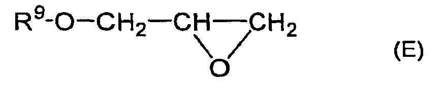
- Di-epoxy-terminated silicon-free organic compounds of the formula F:

- Unsaturated silicon-free organic compounds of the formula G:
CX9X10=CX11X12 (g)
which include carbon and hydrogen as essential components. - In the formulae E and F, R9 is a hydrogen atom or a hydrocarbon group having 1 to 10 carbon atoms which may include oxygen and R10 is a divalent hydrocarbon group having 1 to 7 carbon atoms which may include oxygen.
- In the formula G, X9 to X12 are each independently a hydrogen atom, a hydrocarbon group having 1 to 10 carbon atoms, or an organic group having 1 to 10 carbon atoms which include carbon atom and hydrogen atom as essential components and further include at least one of oxygen atom and nitrogen atom as an essential component. Examples of the hydrocarbon groups as R9 and X9 to X12 include methyl, ethyl, n-propyl, isopropyl and n-butyl.
- Examples of the divalent hydrocarbon group as R10 include methylene, ethylene, n-propylene, isopropylene and n-butylene.
- Examples of the organic groups as X9 to X12 include an amino group, an epoxy group, a carboxyl group and a polyether group.
- The optical member produced by the process of the present invention is preferably a plastic lens.
- The present invention is described in more detail by referring to the following examples. However, it should be noted that these examples are only illustrative and not intended to limit the invention thereto.
- The properties of the optical members obtained in the following examples and comparative examples were evaluated by the following methods.
- The luminous transmittance Y of a plastic lens having an anti-reflection film on both surfaces was measured by Hitachi Spectrophotometers "U-4100" and "U-3410".
- The luminous reflectance Z of a plastic lens having an anti-reflection film on both surfaces was measured by Hitachi Spectrophotometers "U-4100" and "U-3410".
- A lens having a central thickness (CT) of 1.0 mm or 2.0 mm and a refractive power of 0.00 D (diopter) was produced and subjected to a drop ball test prescribed by FDA (Food and Drug Administration). The results were evaluated according to the following ratings.
- A: Accepted
- B: Rejected
- The weight of the ball was 16 g. The lens suffered from cracks or fracture after the drop ball test was made "rejected," and the lens exhibiting no change in the appearance even after the drop ball test was made "accepted."
- The surface of a plastic lens was cross-cut by a razor to form 100 squares (1 mm x 1 mm). Apiece of cellophane tape available from Nichiban Co., Ltd., was attached onto the cross-cut surface, and then, rapidly peeled off. The adhesion strength was evaluated by the rate of the residual squares (the number of residual squares/100).
- The surface of the plastic lens was rubbed with a steel wool (#0000 available from Nihon Steel Wool Co., Ltd.) under a load of 1 kgf/cm2 (0.1 MPa) in 10 strokes and then the surface was observed. The results were evaluated according to the following ratings.
- UA: Substantially no scores
- A: Several thin scores
- B: Many thin scores and several thick scores
- C: Many thin scores and many thick scores
- D: Substantial peeling off of the film
- The plastic lens was heated in a dry oven for 1 h while raising the temperature at intervals of 5°C from 60°C to determine the temperature at which cracks occurred.
- A plastic lens was immersed in a 10 wt % NaOH aqueous solution at 20°C for 1 h and then the surface was observed. The results were evaluated according to the following ratings.
- UA: Substantially no change
- A: Several dot-like peelings
- B: Dot-like peelings throughout the surface
- C: Dot-like peelings throughout the surface and several scale-like peelings
- D: Substantial peeling off of the film
- Using a BTE Abrasion Tester (tradename; available from Colts Inc. (US)) and a haze meter available from Murakami Color Research Laboratory Co., Ltd., the difference in haze value between sample lenses and reference lenses was measured to determine the Bayer value.
Number of Samples and Measuring Method - (a) Three reference lenses (CR39) and three sample lenses.
- (b) Measuring haze values before the abrasion test.
- (c) Performing the abrasion test using the BET abrasion tester (600-stroke of abrasion with sand).
- (d) Measuring haze values after the abrasion test.
- (e) Calculating the Bayer value (average of three lenses) according to the following formula:
- Bayer Value = (Change in transmittance of reference lens)/(Change in transmittance of sample lens).
- The convex surface of a plastic lens was hand-rubbed with a tissue paper 100 times to measure the static voltage using a static charge meter "FMX-002" (tradename) available from Simco Japan Co., Ltd. Since the static voltage varied with time, the static voltage was measured at 5 s, 10 s, 20 s, 40 s, 80 s, 160 s and 320 s after rubbed 100 times. The measured values were fitted by the formula: V1 = V0exp(-at), wherein V1 is the static voltage (V), V0 is the estimated initial static voltage (V), 1/a is the time (second) required for reaching 1/a of the initial static voltage, and t is time (second) passed before the measurement.
- The antistatic effect was evaluated from the results according to the following ratings.
- V0 ≤ 300 V and 1/a ≤ 50 s: Good antistatic effect
- V0 > 300 V or 1/a > 50 s: No antistatic effect
- The treating solution (0.2 cc) was dropped on a slide glass and then spread into a circle of a diameter of 10 mm. Before dried up, the electric resistance was measured by a tester with a test probe distance of about 5 mm. The conductivity was determined by the measured electric resistance.
- The antistatic effect was evaluated according to the following ratings.
- Measured resistance was 10 MΩ or less: Sufficient antistatic effect
- Measured resistance was more than 10 MΩ: Insufficient antistatic effect (11) Water Repellency
- The water repellency was evaluated by the contact angle of water measured using a contact angle meter available from Kyowa Interface Science Co., Ltd.
- Water repellent solutions were prepared from the following raw materials.
Component (a): Water repellent having perfluoroalkyl group - KY130: water repellent available from Shin-Etsu Chemical Co., Ltd. Component (b): Silane coupling agent, modified silicone oil and perfluoroether compound
- KBE903: amino group-containing silane coupling agent available from Shin-Etsu Chemical Co., Ltd.
- KF101: side chain epoxy-modified silicone oil available from Shin-Etsu Chemical Co., Ltd.
- KF105: dz-epoxy-terminated, modified silicone oil available from Shin-Etsu Chemical Co., Ltd.
- HFE7100: perfluoroether compound available from Sumitomo 3M Limited.
- HFE7200: perfluoroether compound available from Sumitomo 3M Limited.
- The chemical structurals of the silane coupling agents, modified silicone oils and perfluoroether compounds are shown below.
- KBE903: (C2H5O)3SiC3H6NH2
- KF101:


- KF105:


- HFE7100: C4F9OCH3
- HFE7200: C3F7OC2H5
- CNT: carbon nanotube (original particle size: 2 to 20 nm) available from The Honjo Chemical Corporation.
- C60 and C70: carbon clusters (original particle size: 5 nm) available from Kanto Kagaku Co., Ltd.
- CBG: conductive carbon black #3855 (original particle size: 24 nm) available from Tokai Carbon Co., Ltd.
- These conductive substances were granulated into particles having a particle size of 20 to 50 µm using an automatic mortar.
-
- 1. A glass container placed with a stirrer was charged with 1.0 g of crashed CNT (CBG or C60/C70). The words "CNT (CBG or C60/C70)" means that CBG, or C60 and/or C70 may be used in place of CNT to obtain the same effect.
- 2. Next, 4 g of KBE903 was charged into the glass container and the contents were stirred for 120 s. The rotating speed of the stirrer was 500 rpm.
- 3. Next, 4 g of KF105 was introduced into the glass container and the contents were stirred for 24 h to prepare Filler A.
- 4. After stirring for 120 min, 3.5 g of Filler A was added to 7.0 g of the water repellent KY130 in a separate container and the contents were stirred for 120 s.
- 5. Then, 3 g of HFE7200 (perfluoroether compound) was added to the glass container and the contents were stirred for 24 h to prepare a treating solution (water repellent solution). The carbon content in the solid component (content of CNT (CBG or C60/C70)) was 7.91% by weight.
- The above procedure is shown in Table 1 below.
Table 1 Step Raw materials Amount used (g) Mixing time 1 Component (c): conductive substance 1.0 - CNT (CBG or C60/C70) 2 Component (b): silane coupling agent 4.0 120 s KBE903 3 Component (b): modified silicone oil 4.0 24 h KF105 4 Adding Filler A to KY130 (component (a): water repellent) 120 s Filler A 3.5 KY130 7.0 5 Component (b)= perfluoroether compound 3.0 24 h HFE7200 - As shown in Tables 2-1/5 to 2-5/5 and Tables 3-1/4 to 3-4/4, each plastic lens having a water-repellent antistatic layer was produced by the following sequential steps:
- step 1 of forming a cured film A or B on each of the plastic lens substrates A to D;
- step 2 of pretreating the cured film by the irradiation of ions;
- step 3 of forming an anti-reflection film composed of 1st to 7th layers on the pretreated film;
- step 4 of pretreating the anti-reflection films by the irradiation of ions; and
- step 5 of forming a thin film (water-repellent antistatic layer) on the anti-reflection film.
- The kinds of materials, production methods and treating methods used in the examples and comparative examples are described below.
-
- Substrate A: diethylene glycol bis(allyl carbonate); refractive index: 1.50; central thickness (CT): 2.0 mm; refractive power: 0.00 D
- Substrate B: EYRY substrate (tradename; available from HOYA Corporation; a polymer of an epithio group-containing compound); refractive index: 1.70; CT: 1.0 mm; refractive power: 0.00 D
- Substrate C: EYNOA substrate (tradename; available from HOYA Corporation; polythiourethane resin); refractive index: 1.67; CT: 1.0 mm; refractive power: 0.00 D
- In Example 2, a primer layer was formed between the substrate and the cured film. The primer layer was formed by the following method.
- A mixture of 6.65 parts by weight of a polyester polyol "Desmophen A-670" (tradename) available from Sumitomo Bayer Urethane Co., Ltd., 6.08 parts by weight of a block polyisocyanate "BL-3175" (tradename) available from Sumitomo Bayer Urethane Co., Ltd., 0.17 part by weight of dibutyltin dilaurate as a curing catalyst, 0.17 part by weight of a fluorine-containing leveling agent "Fluorad FC·430" (tradename) available from Sumitomo 3M Limited, and 95.71 parts by weight of diacetone alcohol as a solvent were fully stirred until reaching a uniform state. The thus obtained liquid primer was applied onto a plastic lens substrate pretreated with an alkali by a dipping method (lifting speed: 24 cm/min), and cured under heating at 100°C for 40 min, to form a primer layer having a thickness of 2 to 3 µm.
- In an atmosphere of 5°C, 45 parts by weight of a methanol sol of a modified stannic oxide-zirconium oxide-tungsten oxide-silicon oxide composite, 15 parts by weight of γ-glycidoxypropyltrimethoxysilane and 3 parts by weight of tetraethoxysilane were mixed under stirring for 1 h. Thereafter, 4.5 parts by weight of a 0.001 mol/L hydrochloric acid was added and then stirred for 50 h. Next, a mixed solvent of 25 parts by weight of propylene glycol monomethyl ether and 9 parts by weight of diacetone alcohol, 1.8 parts by weight of aluminum tris(acetyl acetonate) and 0.05 part by weight of aluminum perchlorate were sequentially added and then stirred for 150 h. The resultant solution was filtered through a 0.5 µm-mesh filter, to obtain a coating composition A.
- The substrate A mentioned above was dipped in a 10 wt% aqueous solution of sodium hydroxide at 60°C for 300 s and then washed with ion-exchanged water for 90 s under exposure to ultrasonic wave of 28 kHz. Finally, the substrate was dried at 70°C, to pretreat the substrate A by a series of the steps.
- The pretreated substrate A was dipped in the coating composition A for 30 s and then lifted therefrom at a rate of 30 cm/min. The coating composition A on the substrate A was cured at 120°C for 60 min, to form a cured film A.
- To 100 parts by weight of γ-glycidoxypropyltrimethoxysilane, 1.4 parts by weight of 0.01 mol/L hydrochloric acid and 23 parts by weight of water were added under stirring. The stirring was continued for 24 h to obtain a hydrolyzate of y-glycidoxypropyltrimethoxysilane. To the hydrolyzate of γ-glycidoxypropyltrimethoxysilane, was added a mixture of 200 parts by weight of a sol of composite fine particles mainly composed of titanium oxide, zirconium oxide and silicon oxide, 100 parts by weight of ethyl cellosolve, 0.5 part by weight of a silicone surfactant and 3.0 parts by weight of aluminum acetylacetonate. The obtained mixture was fully stirred and then filtered, to obtain a coating composition B.
- Each of the substrate B and C pretreated with an aqueous alkali solution was dipped in the coating composition B for 30 s and then lifted therefrom at a rate of 20 cm/min. The coating composition B on the substrate was cured at 120°C for 120 min, to form a cured film B.
- The cured film was pretreated by the ion irradiation using an ion gun under the ion acceleration voltage, irradiation time and gas atmosphere as described in the following Tables.
- After the pretreatment by ion irradiation, the anti-reflection film composed of 1st to 7th layers was formed.
- The hybrid layer was formed by a binary vapor deposition under the conditions controlled so as to deposit the inorganic substance and the organic substance almost simultaneously. The organic substance was vaporized in an external heating tank, and the vaporized organic substance was introduced into a vapor deposition apparatus through a gas valve and a mass-flow controller. The hybrid layer was formed in an argon-oxygen mixed gas atmosphere by an ion-assisted method.
- In the following Tables, CM1 represents an organosilicon compound and CM2 represents a silicon-free organic compound. The organic compounds shown in the Tables are as follows.
- Epolight 70P: propylene glycol diglycidyl ether available from Kyoeisha Chemical Co., Ltd. having a molecular weight of about 188.
- Denacol EX920: polypropylene glycol diglycidyl ether available from Nagase ChemteX Corporation having a molecular weight of about 300.
- Epiol P200: polypropylene glycol glycidyl ether available from NOF Corporation having a molecular weight of about 304.
- The anti-reflection film was pretreated by the ion irradiation using an ion gun under the ion acceleration voltage, irradiation time and gas atmosphere as shown in the following Tables.
- First, film-forming chips were produced from the treating solution obtained in Production Example 1 by injecting 0.3 cc of the treating solution into a SUS bio column using a separate injector and drying at room temperature or 80°C in a dry oven for about 2 h.
- The obtained chips were subjected to vacuum deposition using EB (electron gun) to form a thin film on the anti-reflection film under the following film-forming conditions.
Vapor deposition apparatus: "BMC-1050-HP" available from Shincron Co.,Ltd. Film-forming conditions - Vacuum degree at beginning: 2 x 10⁻³ Pa
- EB output: 20 mA
- "Dotite D-550" (tradename) is a silver-based conductive paste available from Fujikura Kasei Co., Ltd., "Dotite XC-12" (tradename) is a carbon-based conductive paste available from Fujikura Kasei Co., Ltd., and "KP801P" is a water repellent available from Shin-Etsu Chemical Co., Ltd., each being used in comparative examples.
- The tests (1) to (11) were performed on the plastic lenses having the thin films which were formed in the manner described above. The results are shown in Tables 4-1/2 to 4-2/2.
- As shown in Table 4, the treating solutions for plastic lens in Examples 1 to 5 are excellent in the antistatic performance as evidenced by a conductivity of 10 MΩ or less and an initial static voltage of 300 V or less. The water repellency is also excellent as evidence by a water contact angle of 107° or more.
Table 2-1/5 Example 1 Plastic lens substrate Substrate C Cured film Cured film B Ion gun pretreatment Conditions Acceleration voltage: 500V;
Acceleration current: 180 mA; 45 sGas O2: 10 seem + Ar: 10 sccm Anti-reflection film First layer (hybrid layer) Substance (content) M1 SiO2 CM2 Epolight 70P: 10 sccm Film thickness/refractive index 0.0352λ/1.478 Ion gun Conditions Acceleration voltage: 200V;
Acceleration current: 120 mAGas O2: 10 sccm + Ar: 10 sccm Second layer (high refractive index layer) Substance Ta2O5 Film thickness 0.0236λ, Ion gun Conditions Acceleration voltage: 200V;
Acceleration current : 120 mAGas O2: 20 sccm Third layer (hybrid layer) Substance (content) M1 SiO2 CM2 Epolight 70P: 10 sccm Film thickness/refractive index 0.6084λ/1.478 Ion gun Conditions Acceleration voltage: 200V;
Acceleration current: 120 mAGas O2: 10 sccm + Ar: 10 sccm Fourth layer (high refractive index layer) Substance Ta2O5 Film thickness 0.1358λ Ion gun Conditions Acceleration voltage: 200V;
Acceleration current: 120 mAGas O2: 20 sccm Fifth layer (hybrid layer) Substance (content) M1 SiO2 CM2 Epolight 70P: 10 sccm Film thickness/refractive index 0,0606λ/1.478 Ion gun Conditions Acceleration voltage: 200V;
Acceleration current: 120 mAGas O2: 10 sccm + Ar: 10 sccm Sixth layer (high refractive index layer) Substance Ta2O5 Film thickness 0.2520λ Ion gun Conditions Acceleration voltage: 230V;
Acceleration current : 130 mAGas O2: 20 sccm Seventh layer (hybrid layer) Substance (content) M1 SiO2 CM2 Epolight 70P: 10 sccm Film thickness/refractive index 0.2636λ/1.478 Ion gun Conditions Acceleration voltage: 200V;
Acceleration current : 120 mAGas O2: 10 sccm + Ar: 10 seem Ion gun pretreatment Conditions Acceleration voltage: 200V;
Acceleration current: 120 mA; 45 sGas O2: 5 sccm + Ar: 15 sccm Thin film (water-repellent antistatic layer) Substance Treating solution; EB heating Table 2-2/5 Example 2 Plastic lens substrate Substrate B Cured film Cured film B Ion gun pretreatment Conditions Acceleration voltage: 500V;
Acceleration current: 180 mA; 130 sGas O2: 10 sccm + Ar: 10 sccm Anti-reflection film First layer (hybrid layer) Substance (content) M1 SiO2 CM2 Epolight 70P: 20 sccm Film thickness/refractive index 0.0534λ/1.468 Ion gun Conditions Acceleration voltage: 200V;
Acceleration current: 120 mAGas O2: 10 seem + Ar: 10 sccm Second layer (high refractive index layer) Substance Nb2O5 Film thickness 0.0319λ Ion gun Conditions Acceleration voltage: 550V;
Acceleration current: 180 mAGas O2: 20 sccm Third layer (hybrid layer) Substance (content) M1 SiO2 CM2 Epolight 70P: 20 sccm Film thickness/refractive index 0.5452λ/1.468 Ion gun Conditions Acceleration voltage: 200V;
Acceleration current: 120 mAGas O2: 10 sccm + Ar: 10 sccm Fourth layer (high refractive index layer) Substance Nb2O5 Film thickness 0.1001λ Ion gun Conditions Acceleration voltage: 550V;
Acceleration current: 180 mAGas O2: 20 sccm Fifth layer (hybrid layer) Substance (content) M1 SiO2 CM2 Epolight 70P: 20 sccm Film thickness/refractive index 0.1094λ/1.468 Ion gun Conditions Acceleration voltage: 200V;
Acceleration current: 120 mAGas O2: 10 sccm + Ar: 10 sccm Sixth layer (high refractive index layer) Substance Nb2O5 Film thickness 0.1497λ Ion gun Conditions Acceleration voltage: 550V;
Acceleration current: 180 mAGas O2: 20 sccm Seventh layer (hybrid layer) Substance M1 SiO2 (content) CM2 Epolight 70P: 20 sccm Film thickness/refractive index 0.2892λ/1.468 Ion gun Conditions Acceleration voltage: 200V;
Acceleration current: 120 mAGas O2: 10 sccm + Ar: 10 sccm Ion gun pretreatment Conditions Acceleration voltage: 200V;
Acceleration current: 120 mA; 45 sGas O2: 5 sccm + Ar: 15 sccm Thin film (water-repellent antistatic layer) Substance Treating solution; EB heating Table 2-3/5 Example 3 Plastic lens substrate Substrate C Cured film Cured film B Ion gun pretreatment Conditions Acceleration voltage: 500V;
Acceleration current: 180 mA; 45 sGas O2: 10 sccm + Ar: 10 sccm Anti-reflection film First layer (hybrid layer) Substance M1 SiO2 (content) CM2 Epolight 70P: 10 sccm Film thickness/refractive index 0.0352λ/1.478 Ion gun Conditions Acceleration voltage: 200V;
Acceleration current: 120 mAGas O2: 10 sccm + Ar: 10 sccm Second layer (high refractive index layer) Substance Ta2O5 Film thickness 0.0236λ Ion gun Conditions Acceleration voltage: 200V;
Acceleration current: 120 mAGas O2: 20 sccm Third layer (hybrid layer) Substance (content) M1 SiO2 CM2 Epolight 70P: 10 sccm Film thickness/refractive index 0.6084λ/1.478 Ion gun Conditions Acceleration voltage: 200V;
Acceleration current: 120 mAGas O2: 10 sccm + Ar: 10 seem Fourth layer (high refractive index layer) Substance Ta2O5 Film thickness 0.1358λ Ion gun Conditions Acceleration voltage: 200V;
Acceleration current: 120 mAGas O2: 20 seem Fifth layer (hybrid layer) Substance (content) M1 SiO2 CM2 Epolight 70P: 10 seem Film thickness/refractive index 0.0606λ/1.478 Ion gun Conditions Acceleration voltage: 200V;
Acceleration current: 120 mAGas O2: 10 sccm + Ar: 10 sccm Sixth layer (high refractive index layer) Substance Ta2O5 Film thickness 0.2520λ Ion gun Conditions Acceleration voltage: 230V;
Acceleration current: 130 mAGas O2: 20 sccm Seventh layer (hybrid layer) Substance (content) M1 SiO2 CM2 Epolight 70P: 10 sccm Film thickness/refractive index 0.2636λ/1.478 Ion gun Conditions Acceleration voltage: 200V;
Acceleration current: 120 mAGas O2: 10 sccm + Ar: 10 sccm Ion gun pretreatment Conditions Acceleration voltage: 200V;
Acceleration current: 120 mA; 45 sGas O2: 5 sccm + Ar: 15 sccm Thin film (water-repellent antistatic layer) Substance Treating solution; EB heating Table 2-4/5 Example 4 Plastic lens substrate Substrate A Cured film Cured film A Ion gun pretreatment Conditions Acceleration voltage: 500V;
Acceleration current: 180 mA; 45 sGas O2: 10 sccm + Ar: 10 sccm Anti-reflection film First layer (hybrid layer) Substance (content) M1 SiO2 CM2 Epolight 70P: 10 sccm Film thickness/refractive index 0.0352λ/1.478 Ion gun Conditions Acceleration voltage: 200V;
Acceleration current: 120 mAGas O2: 10 sccm + Ar: 10 sccm Second layer (high refractive index layer) Substance Ta2O5 Film thickness 0.0236λ Ion gun Conditions Acceleration voltage: 200V;
Acceleration current: 120 mAGas O2: 20 seem Third layer (hybrid layer) Substance (content) M1 SiO2 CM2 Epolight 70P: 10 sccm Film thickness/refractive index 0.6084λ/1.478 Ion gun Conditions Acceleration voltage: 200V;
Acceleration current: 120 mAGas O2: 10 seem + Ar: 10 sccm Fourth layer (high refractive index layer) Substance Ta2O5 Film thickness 0.1358λ Ion gun Conditions Acceleration voltage: 200V;
Acceleration current : 120 mAGas O2: 20 sccm Fifth layer (hybrid layer) Substance (content) M1 SiO2 CM2 Epolight 70P: 10 sccm Film thickness/refractive index 0.0606λ/1.478 Ion gun Conditions Acceleration voltage: 200V;
Acceleration current: 120 mAGas O2: 10 sccm + Ar: 10 sccm Sixth layer (high refractive index layer) Substance Ta2O5 Film thickness 0.2520λ Ion gun Conditions Acceleration voltage: 230V;
Acceleration current: 130 mAGas O2: 20 sccm Seventh layer (hybrid layer) Substance (content) M1 SiO2 CM2 Epolight 70P: 10 sccm Film thickness/refractive index 0.2636λ/1.478 Ion gun Conditions Acceleration voltage: 200V;
Acceleration current: 120 mAGas O2: 10 sccm + Ar: 10 sccm Ion gun pretreatment Conditions Acceleration voltage: 200V;
Acceleration current: 120 mA; 45 sGas O2: 5 sccm + Ar: 15 sccm Thin film (water-repellent antistatic layer) Substance Treating solution; EB heating Table 2-5/5 Example 5 Plastic lens substrate Substrate A Cured film Cured film A Ion gun pretreatment Conditions Acceleration voltage: 500V;
Acceleration current: 180 mA; 45 sGas O2: 10 sccm + Ar: 10 sccm Anti-reflection film First layer (hybrid layer) Substance (content) M1 SiO2 CM2 Epolight 70P: 10 sccm Film thickness/refractive index 0.0352λ/1.478 Ion gun Conditions Acceleration voltage: 200V;
Acceleration current: 120 mAGas O2: 10 sccm + Ar: 10 seem Second layer (high refractive index layer) Substance Ta2O5 Film thickness 0.0236λ Ion gun Conditions Acceleration voltage: 200V;
Acceleration current: 120 mAGas O2: 20 seem Third layer (hybrid layer) Substance (content) M1 SiO2 CM2 Epolight 70P: 10 sccm Film thickness/refractive index 0.6084λ/1.478 Ion gun Conditions Acceleration voltage: 200V;
Acceleration current: 120 mAGas O2: 10 sccm + Ar: 10 sccm Fourth layer (high refractive index layer) Substance Ta2O5 Film thickness 0.1358λ. Ion gun Conditions Acceleration voltage: 200V;
Acceleration current: 120 mAGas O2: 20 sccm Fifth layer (hybrid layer) Substance (content) M1 SiO2 CM2 Epolight 70P: 10 sccm Film thickness/refractive index 0.0606λ/1.478 Ion gun Conditions Acceleration voltage: 200V;
Acceleration current: 120 mAGas O2: 10 sccm + Ar: 10 sccm Sixth layer (high refractive index layer) Substance Ta2O5 Film thickness 0.2520λ, Ion gun Conditions Acceleration voltage: 230V;
Acceleration current: 130 mAGas O2: 20 sccm Seventh layer (hybrid layer) Substance M1 SiO2 (content) CM2 Epolight 70P: 10 sccm Film thickness/refractive index 0.2636λ/1.478 Ion gun Conditions Acceleration voltage: 200V;
Acceleration current: 120 mAGas O2: 10 sccm + Ar: 10 sccm Ion gun pretreatment Conditions Acceleration voltage: 200V;
Acceleration current: 120 mA; 45 sGas O2: 5 sccm + Ar: 15 sccm Thin film (water-repellent antistatic layer) Substance Treating solution; EB heating Table 3-1/4 Comparative Example 1 Plastic lens substrate Substrate C Cured film Cured film B Ion gun pretreatment Conditions Acceleration voltage: 500V;
Acceleration current: 180 mA; 45 sGas O2: 10 sccm + Ar: 10 sccm Anti-reflection film First layer (hybrid layer) Substance (content) M1 SiO2 CM2 Epolight 70P: 14 sccm Film thickness/refractive index 0.0352λ/1.478 Ion gun Conditions Acceleration voltage: 200V;
Acceleration current: 120 mAGas O2: 10 sccm + Ar: 10 sccm Second layer (high refractive index layer) Substance Ta2O5 Film thickness 0.0236λ Ion gun Conditions Acceleration voltage: 200V;
Acceleration current: 120 mAGas O2: 20 seem Third layer (hybrid layer) Substance (content) M1 SiO2 CM2 Epolight 70P: 14 sccm Film thickness/refractive index 0.6084λ/1.478 Ion gun Conditions Acceleration voltage: 200V;
Acceleration current: 120 mAGas O2: 10 sccm + Ar: 10 sccm Fourth layer (high refractive index layer) Substance Ta2O5 Film thickness 0.1358λ Ion gun Conditions Acceleration voltage: 200V;
Acceleration current: 120 mAGas O2: 20 seem Fifth layer (hybrid layer) Substance M1 SiO2 (content) CM2 Epolight 70P: 14 sccm Film thickness/refractive index 0.0606λ/1.478 Ion gun Conditions Acceleration voltage: 200V;
Acceleration current: 120 mAGas O2: 10 sccm + Ar: 10 sccm Sixth layer (high refractive index layer) Substance Ta2O5 Film thickness 0.2520λ Ion gun Conditions Acceleration voltage: 230V;
Acceleration current: 130 mAGas O2: 20 sccm Seventh layer (hybrid layer) Substance (content) M1 SiO2 CM2 Epiol P200: 14 seem Film thickness/refractive index 0.2636λ/1.478 Ion gun Conditions Acceleration voltage: 200V;
Acceleration current: 120 mAGas O2: 10 sccm + Ar: 10 sccm Ion gun pretreatment Conditions Acceleration voltage: 200V;
Acceleration current: 120 mA; 45 sGas O2: 5 seem + Ar: 15 seem Water-repellent layer Substance KY-130 (or KP801M) Table 3-2/4 Comparative Example 2 Plastic lens substrate Substrate C Cured film Cured film B Ion gun pretreatment Conditions Acceleration voltage: 500V;
Acceleration current: 180 mA; 45 sGas O2: 10 sccm + Ar: 10 sccm Anti-reflection film First layer (hybrid layer) Substance M1 SiO2 (content) CM2 Epolight 70P: 14 sccm Film thickness/refractive index 0.0352λ/1.478 Ion gun Conditions Acceleration voltage: 400V;
Acceleration current: 170 mAGas O2: 10 sccm + Ar: 10 sccm Second layer (high refractive index layer) Substance Ta2O5 Film thickness 0.0236λ. Ion gun Conditions Acceleration voltage: 200V;
Acceleration current: 120 mAGas O2: 20 sccm Third layer (hybrid layer) Substance M1 SiO2 + Al2O3 (content) CM2 Epolight 70P: 14 sccm Film thickness/refractive index 0.6084λ/1.471 Ion gun Conditions Acceleration voltage: 400V;
Acceleration current: 170 mAGas O2: 10 seem + Ar: 10 sccm Fourth layer (high refractive index layer) Substance Ta2O5 Film thickness 0.1358λ Ion gun Conditions Acceleration voltage: 200V;
Acceleration current: 120 mAGas O2: 20 sccm Fifth layer (hybrid layer) Substance (content) M1 SiO2 CM2 Epolight 70P: 14 sccm Film thickness/refractive index 0.0606λ/1.478 Ion gun Conditions Acceleration voltage: 400V;
Acceleration current: 170 mAGas O2: 10 sccm + Ar: 10 seem Sixth layer (high refractive index layer) Substance Ta2O5 Film thickness 0.2520λ Ion gun Conditions Acceleration voltage: 230V;
Acceleration current: 130 mAGas used O2: 20 sccm Seventh layer (hybrid layer) Substance (content) M1 SiO2 CM2 Epolight 70P: 14 sccm Film thickness/refractive index 0.2636λ/1.478 Ion gun Conditions Acceleration voltage: 400V;
Acceleration current: 170 mAGas O2: 10 sccm + Ar: 10 sccm Ion gun pretreatment Conditions Acceleration voltage: 200V;
Acceleration current: 120 mA; 45 sGas O2: 5 sccm + Ar: 15 sccm Water-repellent layer Substance KY-130 (or KP801M) Table 3-3/4 Comparative Example 3 Plastic lens substrate Substrate C Cured film Cured film B Ion gun pretreatment Conditions Acceleration voltage: 500V;
Acceleration current: 180 mA; 45 sGas O2: 10 sccm + Ar: 10 sccm Anti-reflection film First layer (hybrid layer) Substance (content) M1 SiO2 CM2 Epolight 70P: 14 sccm Film thickness/refractive index 0.0352λ/1.478 Ion gun Conditions Acceleration voltage: 200V;
Acceleration current: 120 mAGas O2: 10 sccm + Ar: 10 sccm Second layer (high refractive index layer) Substance Ta2O5 Film thickness 0.0236λ Ion gun Conditions Acceleration voltage: 200V;
Acceleration current: 120 mAGas O2: 20 sccm Third layer (hybrid layer) Substance (content) M1 SiO2 CM2 Epolight 70P: 14 sccm Film thickness/refractive index 0.6084λ/1.478 Ion gun Conditions Acceleration voltage: 200V;
Acceleration current: 120 mAGas O2: 10 seem + Ar: 10 sccm Fourth layer (high refractive index layer) Substance Ta2O5 Film thickness 0.1358λ Ion gun Conditions Acceleration voltage: 200V;
Acceleration current: 120 mAGas O2: 20 sccm Fifth layer (hybrid layer) Substance (content) M1 SiO2 CM2 Epolight 70P: 14 sccm Film thickness/refractive index 0.0606λ/1.478 Ion gun Conditions Acceleration voltage: 200V;
Acceleration current: 120 mAGas O2: 10 sccm + Ar: 10 sccm Sixth layer (high refractive index layer) Substance Ta2O5 Film thickness 0.2520λ Ion gun Conditions Acceleration voltage: 230V;
Acceleration current: 130 mAGas O2: 20 sccm Seventh layer (hybrid layer) Substance (content) M1 SiO2 CM2 Epolight 70P: 14 sccm Film thickness/refractive index 0.2636λ/1.478 Ion gun Conditions Acceleration voltage: 200V;
Acceleration current: 120 mAGas O2: 10 sccm + Ar: 10 sccm Ion gun for pretreatment Conditions Acceleration voltage: 200V;
Acceleration current: 120 mA; 45 sGas O2: 5 sccm + Ar: 15 sccm Water-repellent layer Substance KY-130; Dotite D-550; dipped product obtained by dipping in 10 wt% butyl acetate diluted solution for 30 s. Table 3-4/4 Comparative Example 4 Plastic lens substrate Substrate C Cured film Cured film B Ion gun pretreatment Conditions Acceleration voltage: 500V;
Acceleration current: 180 mA; 45 sGas O2: 10 sccm + Ar: 10 sccm Anti-reflection film First layer (hybrid layer) Substance (content) M1 SiO2 CM2 Epolight 70P:14 sccm Film thickness/refractive index 0.0352λ/1.478 Ion gun Conditions Acceleration voltage: 200V;
Acceleration current: 120 mAGas O2: 10 sccm + Ar: 10 sccm Second layer (high refractive index layer) Substance Ta2O5 Film thickness 0.0236λ Ion gun Conditions Acceleration voltage: 200V;
Acceleration current: 120 mAGas O2: 20 sccm Third layer (hybrid layer) Substance (content) M1 SiO2 CM2 Epolight 70P: 14 sccm Film thickness/refractive index 0.6084λ/1.478 Ion gun Conditions Acceleration voltage: 200V;
Acceleration current: 120 mAGas O2: 10 sccm + Ar: 10 seem Fourth layer (high refractive index layer) Substance Ta2O5 Film thickness 0.1358λ Ion gun Conditions Acceleration voltage: 200V;
Acceleration current: 120 mAGas O2: 20 sccm Fifth layer (hybrid layer) Substance (content) M1 SiO2 CM2 Epolight 70P: 14 sccm Film thickness/refractive index 0.0606λ/1.478 Ion gun Conditions Acceleration voltage: 200V;
Acceleration current: 120 mAGas O2: 10 sccm + Ar: 10 sccm Sixth layer (high refractive index layer) Substance Ta2O5 Film thickness 0.2520λ. Ion gun Conditions Acceleration voltage: 230V;
Acceleration current: 130 mAGas O2: 20 sccm Seventh layer (hybrid layer) Substance (content) M1 SiO2 CM2 Epolight 70P: 14 sccm Film thickness/refractive index 0.2636λ/1.478 Ion gun Conditions Acceleration voltage: 200V;
Acceleration current: 120 mAGas O2: 10 sccm + Ar: 10 sccm Ion gun pretreatment Conditions Acceleration voltage: 200V;
Acceleration current: 120 mA; 45 sGas O2: 5 sccm + Ar: 15 sccm Water-repellent layer Substance KY-130; Dotite XC-12; dipped product obtained by dipping in 10 wt% butyl acetate diluted solution for 30 s. Table 4-1/2 Examples 1 2 3 4 5 Luminous 0.82 0.82 0.82 0.98 0.82 transmittance Y (%) Luminous 99.0 99.0 99.0 99.0 99.0 transmittance Z (%) Impact resistance CT=1.0 CT=1.0 CT=1.0 CT=2.0 CT=1.0 FDA: A FDA: A FDA: A FDA: A FDA: A Adhesion property 100/100 100/100 100/100 100/100 100/100 Abrasion resistance UA UA UA UA UA Heat resistance (°C) 105 85 120 60 85 Alkali resistance UA UA UA UA UA Bayer value 12.0 12.0 12.5 12.0 12.0 Initial static voltage 200 220 200 180 220 (V) 1/a Reduction period 20 20 30 30 20 (s) Conductivity of 1 to 5 1 to 5 1 to 5 1 to 5 1 to 5 treating solution (MΩ) Water repellency 108 107 108 108 108 (water contact angle (°)) Table 4-2/2 Comparative Examples 1 2 3 4 Luminous 0.82 0.82 0.82 0.82 transmittance Y (%) Luminous 99.0 99.0 99.0 99.0 transmittance Z (%) Impact resistance CT=1.0 CT=1.0 CT=1.0 CT=1.0 FDA: A FDA: A FDA: A FDA: A Adhesion property 100/100 100/100 100/100 100/100 Abrasion resistance UA UA UA UA Heat resistance (°C) 105 105 105 105 Alkali resistance UA UA UA UA Bayer value 12.0 12.0 12.0 12.0 Initial static voltage 2000 2000 2000 2000 (V) 1/a Reduction period 300 300 300 300 (s) Conductivity of ∞ ∞ ∞ ∞ treating solution 10% diluted 10% diluted (MΩ) solution solution Water repellency 108 107 107 108 (water contact angle (°)) - As described above, according to the process of the present invention, a thin film and an optical member which are free from discoloration of lens and exhibit a good antistatic property and a good water repellency are obtained. Therefore, the obtained optical member is extremely useful as a plastic lens, etc.

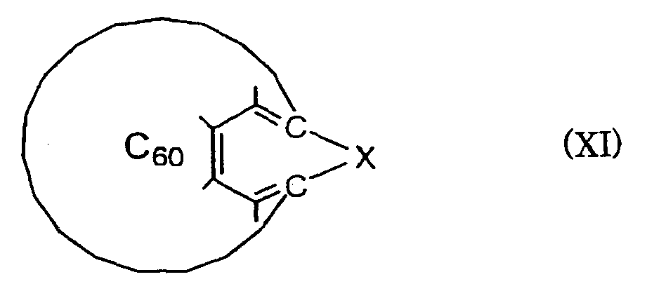
Claims (14)
- A process for producing a thin film by a vacuum deposition method using a water repellent solution, the water repellent solution being prepared by mixing (a) a water repellent having a perfluoroalkyl group, (b) a mixture of a silane coupling agent, a modified silicone oil introduced with an organic group into its side chain and/or both terminal ends, and a perfluoroether compound, and (c) at least one conductive substance selected from the group consisting of fullerenes, carbon nanotubes and graphite compounds.
- The process according to claim 1, wherein the perfluoroether compound is represented by the following formula VIII:
CnF2n+1OCnH2n+1 (VIII)
wherein n and n' are each independently an integer of 1 or more. - The process according to claim 1 or 2, wherein the silane coupling agent is presented by the following formula V:
R1 nSi(OR2)4-n (V)
wherein R1 is a monovalent hydrocarbon group having 1 to 20 carbon atoms which may have a functional group; R2 is an alkyl group having 1 to 8 carbon atoms, an aryl group having 6 to 10 carbon atoms, an aralkyl group having 7 to 10 carbon atoms or an acyl group having 2 to 10 carbon atoms; and n is 0, 1 or 2 with the proviso that a plurality of R1 groups may be the same or different and a plurality of R2O groups may be the same or different. - The process according to claim 3, wherein the silane coupling agent is an aminopropyltrialkoxysilane.
- The process according to claim 4, wherein the aminopropyltrialkoxysilane is aminopropyltrimethoxysilane or aminopropyltriethoxysilane.
- The process according to any one of claims 1 to 5, wherein the modified silicone oil is represented by the following formula VI:


- The process according to any one of claims 1 to 6, wherein the fullerene is at least one compound selected from the group consisting of compounds having a Cz spherical structure wherein z is an integer of from 40 to 120.
- The process according to claim 7, wherein the fullerene is at least one compound selected from the group consisting of compounds having a C60 and C72 spherical structure.
- The process according to any one of claims 1 to 8, wherein the carbon nanotube is at least one compound selected from the group consisting of a multi-walled carbon nanotube and a single-walled carbon nanotube.
- The process according to any one of claims 1 to 8, wherein the graphite compound is at least one compound selected from the group consisting of carbon graphite, fluorinated graphite and expanded graphite.
- The process according to any one of claims 1 to 10, wherein the fullerene, the carbon nanotube and the graphite compound respectively have a particle size of 80 µm or less.
- The process according to any one of claims 1 to 11, wherein the water repellent solution is impregnated into a sintered filter made of a porous material, and the thin film is formed by heating the sintered filter in vacuum.
- A process for producing an optical member, comprising:a step of forming a multilayer anti-reflection film on an optical substrate; anda step of forming a thin film on the multilayer anti-reflection film by a vacuum deposition of a water repellent solution which comprises (a) a water repellent having a perfluoroalkyl group, (b) a mixture of a silane coupling agent, a modified silicone oil introduced with an organic group into its side chain and/or both terminal ends, and a perfluoroether compound, and (c) at least one conductive substance selected from the group consisting of fullerenes, carbon nanotubes and graphite compounds.
- The process according to claim 13, wherein the optical member is a plastic lens.
Priority Applications (2)
| Application Number | Priority Date | Filing Date | Title |
|---|---|---|---|
| EP07010277A EP1995611B1 (en) | 2007-05-23 | 2007-05-23 | Processes for producing thin films and optical members |
| DE602007006640T DE602007006640D1 (en) | 2007-05-23 | 2007-05-23 | Process for the preparation of thin films and optical elements |
Applications Claiming Priority (1)
| Application Number | Priority Date | Filing Date | Title |
|---|---|---|---|
| EP07010277A EP1995611B1 (en) | 2007-05-23 | 2007-05-23 | Processes for producing thin films and optical members |
Publications (2)
| Publication Number | Publication Date |
|---|---|
| EP1995611A1 true EP1995611A1 (en) | 2008-11-26 |
| EP1995611B1 EP1995611B1 (en) | 2010-05-19 |
Family
ID=38623987
Family Applications (1)
| Application Number | Title | Priority Date | Filing Date |
|---|---|---|---|
| EP07010277A Not-in-force EP1995611B1 (en) | 2007-05-23 | 2007-05-23 | Processes for producing thin films and optical members |
Country Status (2)
| Country | Link |
|---|---|
| EP (1) | EP1995611B1 (en) |
| DE (1) | DE602007006640D1 (en) |
Cited By (3)
| Publication number | Priority date | Publication date | Assignee | Title |
|---|---|---|---|---|
| EP2434314A4 (en) * | 2009-05-20 | 2012-10-17 | Tokai Optical Co Ltd | Optical product and plastic lens for eyeglass |
| CN103146305A (en) * | 2011-11-30 | 2013-06-12 | 信越化学工业株式会社 | Fluorine-based surface treating agent for vapor deposition and article finished with the surface treating agent by vapor deposition |
| CN114622169A (en) * | 2022-04-27 | 2022-06-14 | 华天慧创科技(西安)有限公司 | Antifouling film coating device and antifouling film coating method |
Citations (4)
| Publication number | Priority date | Publication date | Assignee | Title |
|---|---|---|---|---|
| EP1074859A2 (en) * | 1999-08-04 | 2001-02-07 | Tomoegawa Paper Co. Ltd. | Anti-reflective material |
| US20030029357A1 (en) * | 2001-08-02 | 2003-02-13 | Shi-Sheng Wang | High contrast, moisture resistant antistatic/antireflective coating for CRT display screen |
| EP1300433A2 (en) * | 2001-10-05 | 2003-04-09 | Shin-Etsu Chemical Co., Ltd. | Perfluoropolyether-modified silane, surface treating agent, and antireflection filter |
| JP2007056314A (en) * | 2005-08-24 | 2007-03-08 | Hoya Corp | Method for producing thin film and optical member |
-
2007
- 2007-05-23 DE DE602007006640T patent/DE602007006640D1/en active Active
- 2007-05-23 EP EP07010277A patent/EP1995611B1/en not_active Not-in-force
Patent Citations (4)
| Publication number | Priority date | Publication date | Assignee | Title |
|---|---|---|---|---|
| EP1074859A2 (en) * | 1999-08-04 | 2001-02-07 | Tomoegawa Paper Co. Ltd. | Anti-reflective material |
| US20030029357A1 (en) * | 2001-08-02 | 2003-02-13 | Shi-Sheng Wang | High contrast, moisture resistant antistatic/antireflective coating for CRT display screen |
| EP1300433A2 (en) * | 2001-10-05 | 2003-04-09 | Shin-Etsu Chemical Co., Ltd. | Perfluoropolyether-modified silane, surface treating agent, and antireflection filter |
| JP2007056314A (en) * | 2005-08-24 | 2007-03-08 | Hoya Corp | Method for producing thin film and optical member |
Cited By (5)
| Publication number | Priority date | Publication date | Assignee | Title |
|---|---|---|---|---|
| EP2434314A4 (en) * | 2009-05-20 | 2012-10-17 | Tokai Optical Co Ltd | Optical product and plastic lens for eyeglass |
| EP3059617A1 (en) * | 2009-05-20 | 2016-08-24 | Tokai Optical Co., Ltd. | Optical product and spectacle plastic lens |
| CN103146305A (en) * | 2011-11-30 | 2013-06-12 | 信越化学工业株式会社 | Fluorine-based surface treating agent for vapor deposition and article finished with the surface treating agent by vapor deposition |
| CN103146305B (en) * | 2011-11-30 | 2017-03-01 | 信越化学工业株式会社 | Fluorine-based surface inorganic agent for vapour deposition and carry out modifying the product obtaining by vapour deposition using this surface conditioning agent |
| CN114622169A (en) * | 2022-04-27 | 2022-06-14 | 华天慧创科技(西安)有限公司 | Antifouling film coating device and antifouling film coating method |
Also Published As
| Publication number | Publication date |
|---|---|
| EP1995611B1 (en) | 2010-05-19 |
| DE602007006640D1 (en) | 2010-07-01 |
Similar Documents
| Publication | Publication Date | Title |
|---|---|---|
| US7981471B2 (en) | Processes for producing thin films and optical members | |
| JP6477815B2 (en) | Water-repellent substrate | |
| CN110537116B (en) | Anti-reflection member and method of manufacturing the same | |
| EP2078765B1 (en) | Vapor deposition material, process for producing optical member or plastic lens for spectacle with use thereof, and plastic lens for spectacle | |
| JPWO2008120505A1 (en) | Water repellent articles, architectural window glass and vehicle window glass | |
| CN111032337B (en) | Water-repellent member and method of manufacturing water-repellent member | |
| KR100543222B1 (en) | Optical member and process of producing the same | |
| EP3459980A1 (en) | Fluorine-containing copolymer | |
| WO2020100725A1 (en) | Fluorine-containing ether composition, coating liquid, and article and method for producing same | |
| EP1917547B1 (en) | Plastic lens and method of producing plastic lens | |
| EP1995611B1 (en) | Processes for producing thin films and optical members | |
| JP7480780B2 (en) | Transparent substrate with anti-fouling layer | |
| JP4759377B2 (en) | Method for manufacturing thin film and optical member | |
| US6939613B2 (en) | Optical member, process of producing optical member, and process of producing thin film | |
| EP2184378A1 (en) | Evaporation source, process for producing optical member, and optical member | |
| JP4695943B2 (en) | Method for manufacturing thin film and optical member | |
| JP2009251008A (en) | Optical product and method for producing the same | |
| CN100492056C (en) | Optical article and manufacturing method thereof | |
| JP4279074B2 (en) | Optical member | |
| JP4420476B2 (en) | Composition for surface modification film, surface modification film, filter for display device, display device and method for producing filter for display device | |
| JP2006039007A (en) | Anti-reflective member | |
| JP2008107836A (en) | Process for producing optical member and thin film | |
| JP5992185B2 (en) | Anti-reflective sheet | |
| JP2004226942A (en) | Optical member, method of manufacturing optical member, and method of manufacturing thin film | |
| JP2006276568A (en) | Optical member |
Legal Events
| Date | Code | Title | Description |
|---|---|---|---|
| PUAI | Public reference made under article 153(3) epc to a published international application that has entered the european phase |
Free format text: ORIGINAL CODE: 0009012 |
|
| AK | Designated contracting states |
Kind code of ref document: A1 Designated state(s): AT BE BG CH CY CZ DE DK EE ES FI FR GB GR HU IE IS IT LI LT LU LV MC MT NL PL PT RO SE SI SK TR |
|
| AX | Request for extension of the european patent |
Extension state: AL BA HR MK RS |
|
| 17P | Request for examination filed |
Effective date: 20090126 |
|
| 17Q | First examination report despatched |
Effective date: 20090227 |
|
| AKX | Designation fees paid |
Designated state(s): DE FR GB |
|
| GRAP | Despatch of communication of intention to grant a patent |
Free format text: ORIGINAL CODE: EPIDOSNIGR1 |
|
| GRAS | Grant fee paid |
Free format text: ORIGINAL CODE: EPIDOSNIGR3 |
|
| GRAA | (expected) grant |
Free format text: ORIGINAL CODE: 0009210 |
|
| AK | Designated contracting states |
Kind code of ref document: B1 Designated state(s): DE FR GB |
|
| REG | Reference to a national code |
Ref country code: GB Ref legal event code: FG4D |
|
| REF | Corresponds to: |
Ref document number: 602007006640 Country of ref document: DE Date of ref document: 20100701 Kind code of ref document: P |
|
| PLBE | No opposition filed within time limit |
Free format text: ORIGINAL CODE: 0009261 |
|
| STAA | Information on the status of an ep patent application or granted ep patent |
Free format text: STATUS: NO OPPOSITION FILED WITHIN TIME LIMIT |
|
| 26N | No opposition filed |
Effective date: 20110222 |
|
| REG | Reference to a national code |
Ref country code: DE Ref legal event code: R097 Ref document number: 602007006640 Country of ref document: DE Effective date: 20110221 |
|
| PGFP | Annual fee paid to national office [announced via postgrant information from national office to epo] |
Ref country code: GB Payment date: 20140521 Year of fee payment: 8 |
|
| PGFP | Annual fee paid to national office [announced via postgrant information from national office to epo] |
Ref country code: FR Payment date: 20140509 Year of fee payment: 8 Ref country code: DE Payment date: 20140521 Year of fee payment: 8 |
|
| REG | Reference to a national code |
Ref country code: DE Ref legal event code: R119 Ref document number: 602007006640 Country of ref document: DE |
|
| GBPC | Gb: european patent ceased through non-payment of renewal fee |
Effective date: 20150523 |
|
| REG | Reference to a national code |
Ref country code: FR Ref legal event code: ST Effective date: 20160129 |
|
| PG25 | Lapsed in a contracting state [announced via postgrant information from national office to epo] |
Ref country code: GB Free format text: LAPSE BECAUSE OF NON-PAYMENT OF DUE FEES Effective date: 20150523 Ref country code: DE Free format text: LAPSE BECAUSE OF NON-PAYMENT OF DUE FEES Effective date: 20151201 |
|
| PG25 | Lapsed in a contracting state [announced via postgrant information from national office to epo] |
Ref country code: FR Free format text: LAPSE BECAUSE OF NON-PAYMENT OF DUE FEES Effective date: 20150601 |