EP1990834A2 - Lokale Integration eines nichtlinearen Blechs in integrierten Schaltpaketen für ESD/EOS-Schutz - Google Patents
Lokale Integration eines nichtlinearen Blechs in integrierten Schaltpaketen für ESD/EOS-Schutz Download PDFInfo
- Publication number
- EP1990834A2 EP1990834A2 EP08100931A EP08100931A EP1990834A2 EP 1990834 A2 EP1990834 A2 EP 1990834A2 EP 08100931 A EP08100931 A EP 08100931A EP 08100931 A EP08100931 A EP 08100931A EP 1990834 A2 EP1990834 A2 EP 1990834A2
- Authority
- EP
- European Patent Office
- Prior art keywords
- metal
- terminals
- traces
- insulator
- metal layer
- Prior art date
- Legal status (The legal status is an assumption and is not a legal conclusion. Google has not performed a legal analysis and makes no representation as to the accuracy of the status listed.)
- Granted
Links
Images


Classifications
-
- H—ELECTRICITY
- H10—SEMICONDUCTOR DEVICES; ELECTRIC SOLID-STATE DEVICES NOT OTHERWISE PROVIDED FOR
- H10W—GENERIC PACKAGES, INTERCONNECTIONS, CONNECTORS OR OTHER CONSTRUCTIONAL DETAILS OF DEVICES COVERED BY CLASS H10
- H10W42/00—Arrangements for protection of devices
- H10W42/80—Arrangements for protection of devices protecting against overcurrent or overload, e.g. fuses or shunts
-
- H—ELECTRICITY
- H05—ELECTRIC TECHNIQUES NOT OTHERWISE PROVIDED FOR
- H05K—PRINTED CIRCUITS; CASINGS OR CONSTRUCTIONAL DETAILS OF ELECTRIC APPARATUS; MANUFACTURE OF ASSEMBLAGES OF ELECTRICAL COMPONENTS
- H05K1/00—Printed circuits
- H05K1/02—Details
- H05K1/0213—Electrical arrangements not otherwise provided for
- H05K1/0254—High voltage adaptations; Electrical insulation details; Overvoltage or electrostatic discharge protection ; Arrangements for regulating voltages or for using plural voltages
- H05K1/0257—Overvoltage protection
- H05K1/0259—Electrostatic discharge [ESD] protection
-
- H—ELECTRICITY
- H10—SEMICONDUCTOR DEVICES; ELECTRIC SOLID-STATE DEVICES NOT OTHERWISE PROVIDED FOR
- H10W—GENERIC PACKAGES, INTERCONNECTIONS, CONNECTORS OR OTHER CONSTRUCTIONAL DETAILS OF DEVICES COVERED BY CLASS H10
- H10W42/00—Arrangements for protection of devices
- H10W42/60—Arrangements for protection of devices protecting against electrostatic charges or discharges, e.g. Faraday shields
-
- H—ELECTRICITY
- H05—ELECTRIC TECHNIQUES NOT OTHERWISE PROVIDED FOR
- H05K—PRINTED CIRCUITS; CASINGS OR CONSTRUCTIONAL DETAILS OF ELECTRIC APPARATUS; MANUFACTURE OF ASSEMBLAGES OF ELECTRICAL COMPONENTS
- H05K2201/00—Indexing scheme relating to printed circuits covered by H05K1/00
- H05K2201/07—Electric details
- H05K2201/073—High voltage adaptations
- H05K2201/0738—Use of voltage responsive materials, e.g. voltage switchable dielectric or varistor materials
-
- H—ELECTRICITY
- H10—SEMICONDUCTOR DEVICES; ELECTRIC SOLID-STATE DEVICES NOT OTHERWISE PROVIDED FOR
- H10W—GENERIC PACKAGES, INTERCONNECTIONS, CONNECTORS OR OTHER CONSTRUCTIONAL DETAILS OF DEVICES COVERED BY CLASS H10
- H10W72/00—Interconnections or connectors in packages
- H10W72/90—Bond pads, in general
- H10W72/921—Structures or relative sizes of bond pads
- H10W72/923—Bond pads having multiple stacked layers
-
- H—ELECTRICITY
- H10—SEMICONDUCTOR DEVICES; ELECTRIC SOLID-STATE DEVICES NOT OTHERWISE PROVIDED FOR
- H10W—GENERIC PACKAGES, INTERCONNECTIONS, CONNECTORS OR OTHER CONSTRUCTIONAL DETAILS OF DEVICES COVERED BY CLASS H10
- H10W72/00—Interconnections or connectors in packages
- H10W72/90—Bond pads, in general
- H10W72/941—Dispositions of bond pads
- H10W72/9415—Dispositions of bond pads relative to the surface, e.g. recessed, protruding
-
- H—ELECTRICITY
- H10—SEMICONDUCTOR DEVICES; ELECTRIC SOLID-STATE DEVICES NOT OTHERWISE PROVIDED FOR
- H10W—GENERIC PACKAGES, INTERCONNECTIONS, CONNECTORS OR OTHER CONSTRUCTIONAL DETAILS OF DEVICES COVERED BY CLASS H10
- H10W72/00—Interconnections or connectors in packages
- H10W72/90—Bond pads, in general
- H10W72/941—Dispositions of bond pads
- H10W72/942—Dispositions of bond pads relative to underlying supporting features, e.g. bond pads, RDLs or vias
-
- H—ELECTRICITY
- H10—SEMICONDUCTOR DEVICES; ELECTRIC SOLID-STATE DEVICES NOT OTHERWISE PROVIDED FOR
- H10W—GENERIC PACKAGES, INTERCONNECTIONS, CONNECTORS OR OTHER CONSTRUCTIONAL DETAILS OF DEVICES COVERED BY CLASS H10
- H10W72/00—Interconnections or connectors in packages
- H10W72/90—Bond pads, in general
- H10W72/951—Materials of bond pads
- H10W72/952—Materials of bond pads comprising metals or metalloids, e.g. PbSn, Ag or Cu
-
- H—ELECTRICITY
- H10—SEMICONDUCTOR DEVICES; ELECTRIC SOLID-STATE DEVICES NOT OTHERWISE PROVIDED FOR
- H10W—GENERIC PACKAGES, INTERCONNECTIONS, CONNECTORS OR OTHER CONSTRUCTIONAL DETAILS OF DEVICES COVERED BY CLASS H10
- H10W90/00—Package configurations
- H10W90/701—Package configurations characterised by the relative positions of pads or connectors relative to package parts
- H10W90/721—Package configurations characterised by the relative positions of pads or connectors relative to package parts of bump connectors
- H10W90/724—Package configurations characterised by the relative positions of pads or connectors relative to package parts of bump connectors between a chip and a stacked insulating package substrate, interposer or RDL
-
- Y—GENERAL TAGGING OF NEW TECHNOLOGICAL DEVELOPMENTS; GENERAL TAGGING OF CROSS-SECTIONAL TECHNOLOGIES SPANNING OVER SEVERAL SECTIONS OF THE IPC; TECHNICAL SUBJECTS COVERED BY FORMER USPC CROSS-REFERENCE ART COLLECTIONS [XRACs] AND DIGESTS
- Y10—TECHNICAL SUBJECTS COVERED BY FORMER USPC
- Y10T—TECHNICAL SUBJECTS COVERED BY FORMER US CLASSIFICATION
- Y10T29/00—Metal working
- Y10T29/49—Method of mechanical manufacture
- Y10T29/49002—Electrical device making
- Y10T29/49105—Switch making
Definitions
- the present invention is related in general to the field of electronic systems and semiconductor devices and more specifically to structure and method of local electrostatic discharge protection built into the package of the devices using a non-linear film.
- ESD electrostatic discharge
- other destructive transient effects such as cable discharge events, transient latch-ups, and electrostatic overcharge (EOS)
- ESD electrostatic discharge
- EOS electrostatic overcharge
- Additional ESD challenges are presented by the requirements of high performance/high speed circuits for low leakage and low capacitance of the ESD protection structures; further by the integration, in the same chip, of 5 V USB (Universal Serial Bus) applications with 1.2 V operation (2 nm gate oxide technology); and by the customer demands for external interface IC protection to meet the component-level ESD protection simultaneously with the system-level ESD protection.
- 5 V USB Universal Serial Bus
- the system-level events (IEC, also called Human Metal Model) occur at 4 to 8 kV stress and are equivalent to tens of amps for 1 to 2 ⁇ s; integrated over time, their energy-under-the-pulse is thus many times more severe than the common Human Body Model (HBM).
- HBM Human Body Model
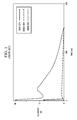
- FIG. 1 shows an IEC pulse at 8 kV; the initial spike looks like a Charged Device Model (CDM) event followed by an HBM-like wave at nearly 15 A, representing energy under the pulse much larger than the common component level ESD pulse like the HBM event at 1kV or 2 kV.
- CDM Charged Device Model
- system-level ESD which is important for device pins interfacing with the outside world, requires external protection devices that have to handle currents in the 30 A range for stress levels as high as 8 kV.
- Other ESD such as Cable Discharge Events (CDE) also introduce very high currents even at 1kV for longer time periods of 1 ps.
- CDE Cable Discharge Events
- U.S. Patents 6,981,319 and 7,218,492 , and U.S. Patent Application Publication 2007/0127175 describe devices and systems for electrostatic discharge suppression based on an electrostatic discharge reactance layer built from a polymer-based suppression material embedded with nanometer-size conducting particles. The material switches from insulating to conducting mode at the high voltages of an overcharge event.
- the device disclosed in the patents uses electrodes embedded in cavities on either side of the electrostatic discharge reactance layer; the electrodes have extensions, which overlap so that they determine the overall protective performance of the device.
- the structure of the embodiments however, has the disadvantages that it does not lend itself to the industry trend of miniaturization and to the market need for fine pitch. Further, the method of fabrication is cumbersome and thus expensive.
- the structure of the prior art has distinct disadvantages.
- the structural complexity, especially the cavities of the electrostatic discharge layer, does not lend itself to design fine-pitched device terminals; also, the overall protection thickness does not facilitate device miniaturization.
- the inherent resistance in the range of few hundred m ⁇ of the protection circuits makes the discharge of the high stress currents in the system-level ESD (IEC) events problematic.
- the fabrication method in prior art is cumbersome and thus expensive; it does not lend itself to mass production and low cost.
- Applicants' investigations identified a method to protect the multitude of electrodes of an integrated circuit chip against electrical overcharge by assembling the chip onto a substrate, which is structured so that it includes a multitude of local, built-in fine-pitch protection shortcuts to bypass electrical overcharge events directly to ground, before they reach the electrodes.
- the shortcuts to ground are fine-pitched and exhibit, as measurements have shown, only a few m ⁇ resistance. They are thus well suited to discharge even the high IEC stress currents found in system-level ESD.
- the very low resistance compares favorably to the few hundred m ⁇ resistance inherent in the structures of the existing technology quoted above.
- the method for fabricating the substrate with the protection bypasses is low cost.
- the method lends itself the batch processing and mass production.
- the substrate has, sandwiched in an insulator, a flat sheet-like sieve member made of a non-linear material that switches from insulator to conductor mode at a preset voltage.
- the member is perforated with through-holes, otherwise both surfaces of the sheet are free of indentations.
- Metal traces over one surface of the sieve member are positioned across a first set of the through-holes; each trace is connected to a terminal on the substrate top and, through the hole, to a terminal on the substrate bottom.
- Metal traces over the opposite member surface are positioned across a second set through-holes; each trace is connected to a terminal on the substrate bottom and, through the hole, to a terminal on the substrate top. The position of the latter traces overlaps with a portion of the first traces. These overlap areas are the locations for the conductivity switches.
- the invention employs a flat sheet of the non-linear material, which extends practically throughout the package and can thus protect even the fine-pitched signal and power pins.
- the solution enabled by the invention saves significant PCB area and is much less expensive than traditional stand-alone protection devices.
- the method of the invention is also less expensive than forming cavities in the non-linear material and embedding metal traces for overlaps in the cavities. Due to the minimized electrical paths, the structure of the invention can carry high discharge currents and offers much faster protection than the stacking of chips containing the ESD protections.
- Another embodiment of the invention is a method for fabricating a semiconductor device with locally integrated protections against transients.
- the method includes providing a long tape, with over its whole length and width a thin (about 3 ⁇ m) flat sheet of non-linear material sandwiched between two metal layers.
- the non-linear material switches from an insulator to a conductor at a preset voltage.
- the first metal layer is etched to create first traces over the non-linear sheet and gaps between the traces.
- the second metal layer is etched to create second traces over the non-linear sheet and gaps.
- the second traces partially overlap with portions of the first traces; the overlap areas are the locations for the conductivity switches.
- An insulator foil with a metal layer facing outward is laminated on each of the first and the second trace, filling the gaps between the traces. This creates a flat tape-like substrate for the sites of a plurality of repetitive devices.
- the through-holes need a set of through-holes in the sheet. Consequently, drilling perforates the sheet with through-holes and turns it into a flat sieve member. Metal (for example, copper) is then deposited to fill the through-holes and to thicken the metal layers.
- the thickened metal layers on the substrate top and bottom are etched to create terminals for the metal-filled through-holes.
- the terminals are distributed, for each device site, between usage for signal and power, and for ground.
- the selection of the signal and power terminals on the substrate bottom is performed so that the trace, to which each terminal is connected, overlaps with a trace on the opposite surface of the sheet, and that the opposite trace is connected to ground.
- an electrostatic overcharge that hits the signal/power terminal will readily initiate a local switching of the sheet material to conductor mode and thus bypass the overcharge to ground without giving the transient a chance to damage the corresponding signal/power terminal and the electronic component on the substrate top.
- This advantage provides protection against transients even for very fine pitch center-to-center of the terminals.
- FIG. 2 illustrates a schematic cross section of an embodiment of the invention, which is an electronic device generally designated 200 with protection against transients.
- Device 100 includes an electronic component 201 connected by solder bodies 210 to a substrate 220.
- Component 201 may be a semiconductor chip, or may be another device in need for protection against electrostatic discharge, system level transients, cable discharge events, transient latch-ups, or any other electrostatic overcharge events.
- chip 201 has metallic electrodes for external connections. According to their electrical function, the electrodes are grouped in sets: First electrodes 202 serve electrical signal and power, and second electrodes 203 serve electrical ground potential (or supply/ground; zero power being equivalent to ground).
- One of the first electrodes is schematically shown with its own protection device 204.
- FIG. 2 also shows a substrate 220, onto which the component 201 is assembled, and which has built-in local ESD protection shortcuts for the first electrodes 202.
- the shortcuts are integral with the substrate and are operable to bypass electrical overcharge events directly to ground.
- Substrate 220 includes insulator material 221 (such as epoxy glass, ABF, etc.) preferably in the thickness range from about 20 to 60 ⁇ m. For some devices it may be thinner or thicker, but driven by handheld and wireless product applications, the overall industry trend is towards thinner thicknesses.
- Substrate 220 has a top surface 220a and a bottom surface 220b. Both top and bottom surfaces have metallic terminals grouped in sets: Top surface 220a has first set terminals 231 and third set terminals 233; and bottom surface 220b has second set terminals 232 and fourth set terminals 234.
- Substrate 220 further includes a flat sheet-like sieve member 240 sandwiched in the insulator 221.
- Sieve member 240 extends throughout the length and width of the device.
- Sieve member 240 is made of a non-linear material, an insulating polymer compound embedded with nanometer-size conducting particles. The compound switches from insulator to conductor mode at a preset voltage, which is mainly determined by the member thickness.
- the member 240 is flat and sheet-like in the thickness range between about 3 and 10 ⁇ m.
- a substrate according to the method of this invention enables the thickness of the sheet to be reduced by about one order of magnitude and still provide adequate ESD protection to the electronic component.
- the non-linear material is commercially available in industry from, for example, Electronic Polymers, Inc., Round Rock, Texas, U.S.A.
- Sieve member 240 has a first surface 240a and a second surface 240b. Both surfaces are free of indentations such as cavities, grooves and trenches so the process of forming a substrate is much simplified comparing to known technology.
- sieve member 240 is perforated by through-holes, which are grouped in sets: first set through-holes are designated 241; second set through-holes are designated 242.
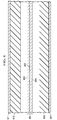
- the flat sheet-like sieve member 301 of an actual semiconductor device is depicted in top view in order to illustrate an example of the high number of through-holes 302, and the extension of the member over the entire length and width of the device.
- the actual size of the square-shaped sieve member in this example is 12 by 12 mm, and the diameter of the through-holes is about 80 ⁇ m. In other devices, the through-holes may have preferred diameters between about 80 to 150 ⁇ m.
- the number and distribution of the through-holes depends on the number and position of device terminals to be protected against ESD events.
- first metal traces 251 On the first surface 240a of sieve member 240 are first metal traces 251, preferably made of copper in the thickness range from about 10 to 25 ⁇ m. Each trace 251 is positioned across a first set through-hole 241 through sieve member 240. Further, each trace 251 has a conductive connection to a third set terminal 233 on the first substrate surface 220a, and, through the respective first set through-hole 241, a conductive connection to a second set terminal 232 on the second substrate surface 220b. In other words, both the connection to the third set terminal 233 and the connection to the second set terminal 232 terminate at trace 251.
- each trace 252 is positioned across a second set through-hole 242 through sieve member 240 so that trace 252 partially overlaps with a portion of at least one first trace 251.
- the overlap areas are the locations for the conductivity switches described above, which provide the local bypass to ground for transient events.
- each trace 252 has a conductive connection to a fourth set terminal 234 on the second substrate surface 220b, and, through the respective second set through-hole 242, a conductive connection to a first set terminal 231 on the first substrate surface 220a. Again, both the connection to the fourth set terminal 234 and the connection to the first set terminal 231 terminate at trace 252.
- FIG. 2 depicts a flip-chip attachment of a component 201 onto substrate 220.
- Solder bodies 210 connect first electrodes 202 and second electrodes 203 of component 201 with the first set terminals 231 and the third set terminals 233 of substrate 220. The connection is so that each first electrode 202 is protected by a low-resistance local bypass built into the substrate 220, which discharges any transient pulse to ground by switching the conductivity of the non-linear material between the overlapping traces.
- Solder bodies 260 may be used to connect the second set terminals 232 to external electrical signal and power, and to connect the fourth set terminals 234 to external electrical ground.
- solder bodies 210 or the solder bodies 260 wire bonding, pressure contacts, or other interconnection means may be used for achieve electrical connection.
- bonding wires it is preferred to also employ an encapsulation material such as a molding compound in order to protect the wires and the component.
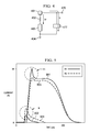
- FIG. 4 and FIG. 5 illustrate the impact of an ultra-low resistance of the local bypass to shortcut the impinging transient pulse to ground before it can endanger a component.
- a substrate terminal designated 401 is connected through path resistance 402 to the non-linear overcharge suppression material 403 and ground 404.
- I m peak current
- Terminal 401 is connected to component/chip electrode (I/O) 410.
- I/O component/chip electrode
- the I/O also has a conventional clamp 411, which is connected to ground 404.
- Clamp 411 has a resistance, which allows a current I c to flow to ground 404.
- FIG. 5 plots current in amperes (A) through both paths as a function of time in nanoseconds (ns) for two resistances.
- the ultra-low resistance of the local bypass puts the value of path resistance 402 in the range of few m ⁇ (R 1 about 2 to 20 m ⁇ .
- the current follows the high-energy curve 501 in FIG. 5 for the bypass, with I m around 30 A, and the low-energy curve 502 for the I/O clamp, with I c only about 4 A.
- the solution of the known technology puts the value of the path resistance 402 in the range over 100 m ⁇ (R 2 between about 0.1 and 2 ⁇ ).
- the current follows curve 503 for the connection to ground, with I m about 20 to 25 A, but the current 504 through the I/O clamp is considerably more stressful with I c about 10 A, which is more likely to damage the electronic component on the substrate.
- Another embodiment of the present invention is a method for fabricating a semiconductor device with protection against transient pulses.
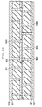
- the method starts with providing a flat tape 601 as depicted in FIG. 6 .
- the tape includes a sheet 602 of a non-linear material sandwiched between a first metal layer 603 and a second metal layer 604.
- the non-linear material is an insulating polymer compound embedded with nanometer-size conducting particles that allow the material to switch from insulator to conductor mode at a preset voltage.
- Sheet 602 is preferably between 3 and 10 ⁇ m thick.
- Metal layers 603 and 604 are preferably copper in the thickness range from about 25 to 100 ⁇ m. The sheet and the metal layers extend over the entire tape length and width.
- the first and second metal layers are patterned in a photolithographic process.
- the first metal 603 layer is etched to create first metal traces 703, which are separated by first gaps 713.
- the second metal layer 604 is etched to create second metal traces 704, separated by second gaps 714.
- the traces are so designed that the second traces 704 extend across the first gaps 713 and partially overlap with portions of the first traces 703. These overlap areas are designated 724 in FIG. 7 ; they are the locations for the conductivity switches of the non-linear sheet with the areas.
- a first insulator foil 610 is provided, which is plated with a third metal layer 611.
- the insulator material may be epoxy glass, ABF, or related compounds, and is preferably between about 20 and 60 ⁇ m thick.
- Metal layer 611 is preferably copper between about 25 and 100 ⁇ m thick.
- first foil 611 is shown just before being placed on the first traces 703, with the third metal layer 611 facing outwardly.
- a second insulator foil 620 is also provided, which is plated with a fourth metal layer 621.
- the insulator is preferably a material like epoxy glass or ABF and has a thickness in the range from about 25 to 100 ⁇ m.
- second foil 620 is shown just before being placed on the second traces 704, with the fourth metal layer 621 facing outwardly.
- the insulators 610 and 620 are laminated unto the metal traces 703 and 704, respectively.
- the gaps 713 between traces 703 and gaps 714 between traces 704 are filled with the insulating material.
- a substrate 801 is formed, which has a flat sheet 602 of non-linear material with partially overlapping metal traces 703 and 704 sandwiched between the insulator 610 and 620, wherein the non-linear material sheet extends throughout the length and width of the tape.
- the substrate offers, after completing the following process steps, a plurality of sites for the assembly of components into a series of repetitive devices.
- results of further process steps are depicted, in which through-holes in the substrate are opened to provide connections to the embedded metal traces.
- a preferred method of opening the through-holes is laser drilling; alternatively, plasma etching or any suitable drilling technique (such as mechanical) may be employed.
- the preferred diameter of the through-holes is between about 3 and 10 ⁇ m - the small size can provide a high density, fine-pitch center-to-center array of through-holes.
- the first set of through-holes is designated 901; they are aligned with the first gaps 713 (see also FIG. 7 ).
- Through-holes 901 extend through the metal layer 611, the insulator foil 610, the insulator-filled gaps 713, and the sheet 602 of non-linear material; terminate at the metal traces 704. Consequently, first through-holes 901 perforate sheet 602 with a first set of through-holes.
- the second set of through-holes are designated 902; the through-holes are aligned with the second gaps 714 (see also FIG. 7 ).
- Through-holes 902 extend through the metal layer 611, the insulator foil 620, the insulator-filled gaps 714, and the sheet 602 of non-linear material; and terminate at the metal traces 703. Consequently, second through-holes 902 perforate sheet 602 with a second set of through-holes.
- FIG. 3 depicts a functional sheet 602 with the combined first and second sets of through-holes.
- the third set of through-holes is designated 903. They extend through metal layer 611 and insulator foil 610, and terminate at the metal traces 703.
- the fourth set of through-holes is designated 904. They extend through metal layer 621 and insulator foil 620, and terminate at the metal traces 704.
- the through-holes are filled with metal, preferably copper.
- metal 1000 is deposited to fill the through-holes of the sets 901, 902, 903, and 904, and, in the same process, to add a continuous (fifth) metal layer 1011 on top of the (third) metal layer 611, and a continuous (sixth) metal layer 1021 on top of the (fourth) metal layer 621.
- the deposited metal (1011, 1021) has the same composition as the metal (611, 621) laminated on the insulator foils
- layer 611 together with layer 1011, and layer 621 together with layer 1021 become metal layers of uniform composition, as depicted in FIG. 2 .
- the metal layers maintain their individual characteristics, as the shading of FIG. 10 suggests.
- the preferred method of depositing metal is plating. Many embodiments add process steps after the deposition, which prepare the surface of metal 1011 to facilitate the later process of attaching solder bodies. For example, one may add thin layers of nickel or nickel and palladium on copper, or attach wire bonds. Further, it is convenient for many embodiments, to add process steps to prepare the surface of metal 1021 to facilitate the later process of attaching solder bodies.
- the metal layers 1011 and 611, and the layers 1021 and 621 are patterned to create terminals for the respective metal-filled through-holes.
- the terminals to be formed from layers 1011 and 611 are destined to be connected to the electrodes of that electrical component, which needs to be protected against overcharge events.
- the terminals to be formed from layers 1021 and 621 are destined to be connected to external signal, power, and ground; they are thus referred to as "external" terminals.
- Preferred patterning techniques include etching by plasma and by chemical processes.
- the patterned terminals are grouped in sets according to the sets, to which the respective metal-filled through-holes belong, which the terminals serve.
- the pattering of the terminals completes the fabrication of substrate 220.
- certain second traces 1252 and their respective fourth set terminals 1234 and first set terminals 1231 are selected for connection to electrical ground.
- the remaining second traces and the first traces, together with their respective terminals (of the fourth set 1234, second set 1232, first set 1231, and third set 1233) are selected for connection to electrical signal and power.
- any overcharge (symbolized by lightning signs 1270) hitting an external substrate terminal for signal/power switches the sheet of non-linear material locally from insulator to conductor mode (symbolized by lightning signs 1271) and is discharged to ground after traveling along a short and localized path of only few m ⁇ resistance.
- a component has electrodes 202 for electrical signal and power, and electrodes 203 for electrical ground (see FIG. 2 ).
- the component electrodes 202 are connected to the site terminals selected for signal and power using solder bodies 210 as shown in FIG. 2 ; or bonding wires 1280 as shown in FIG. 12 .
- the component electrodes 203 are connected to the respective site terminals selected for ground, again using solder bodies 210 as shown in FIG. 2 or bonding wires 1280 as shown in FIG. 12 .
- the connecting steps are repeated for each component, until the assembly of each component on a respective substrate site is completed.
- terminals 1232 and 1234 may be used as pressure contacts for connecting to external parts, since the terminals are flat and positioned in a plane.
- the tape with the assembled components is singulated into discrete devices.
- a preferred technique is sawing.
- the component may be a single semiconductor chip or a stack of chips; the component may belong to a particular product family, such as memory, or it may include a composite functionality.
- the insulator material of the substrate may be more or less flexible, even stiff.
- the pitch center-to-center of the metal-filled through-holes can be reduced so that the invention is effective for many semiconductor device technology nodes and is not restricted to a particular one. It is therefore intended that the appended claims encompass any such modifications or embodiments.
Landscapes
- Engineering & Computer Science (AREA)
- Microelectronics & Electronic Packaging (AREA)
- Semiconductor Integrated Circuits (AREA)
- Structure Of Printed Boards (AREA)
Priority Applications (2)
| Application Number | Priority Date | Filing Date | Title |
|---|---|---|---|
| US12/049,726 US7872841B2 (en) | 2007-05-10 | 2008-03-17 | In package ESD protections of IC using a thin film polymer |
| US12/963,704 US20110075306A1 (en) | 2007-05-10 | 2010-12-09 | Local integration of non-linear sheet i integrated circuit packages for esd/eos protection |
Applications Claiming Priority (1)
| Application Number | Priority Date | Filing Date | Title |
|---|---|---|---|
| US92860407P | 2007-05-10 | 2007-05-10 |
Publications (3)
| Publication Number | Publication Date |
|---|---|
| EP1990834A2 true EP1990834A2 (de) | 2008-11-12 |
| EP1990834A3 EP1990834A3 (de) | 2011-08-31 |
| EP1990834B1 EP1990834B1 (de) | 2012-08-15 |
Family
ID=39494631
Family Applications (1)
| Application Number | Title | Priority Date | Filing Date |
|---|---|---|---|
| EP08100931A Active EP1990834B1 (de) | 2007-05-10 | 2008-01-25 | Lokale Integration eines nichtlinearen Blechs in integrierten Schaltpaketen für ESD/EOS-Schutz |
Country Status (2)
| Country | Link |
|---|---|
| US (2) | US7872841B2 (de) |
| EP (1) | EP1990834B1 (de) |
Cited By (19)
| Publication number | Priority date | Publication date | Assignee | Title |
|---|---|---|---|---|
| US7793236B2 (en) | 2007-06-13 | 2010-09-07 | Shocking Technologies, Inc. | System and method for including protective voltage switchable dielectric material in the design or simulation of substrate devices |
| US7825491B2 (en) | 2005-11-22 | 2010-11-02 | Shocking Technologies, Inc. | Light-emitting device using voltage switchable dielectric material |
| EP2337070A1 (de) * | 2009-12-17 | 2011-06-22 | ABB Technology AG | Elektronische Vorrichtung mit nichtlinearer resistiver Feldabstufung und Verfahren zu ihrer Herstellung |
| US7968010B2 (en) | 2006-07-29 | 2011-06-28 | Shocking Technologies, Inc. | Method for electroplating a substrate |
| US8117743B2 (en) | 1999-08-27 | 2012-02-21 | Shocking Technologies, Inc. | Methods for fabricating current-carrying structures using voltage switchable dielectric materials |
| US8163595B2 (en) | 2006-09-24 | 2012-04-24 | Shocking Technologies, Inc. | Formulations for voltage switchable dielectric materials having a stepped voltage response and methods for making the same |
| US8203421B2 (en) | 2008-04-14 | 2012-06-19 | Shocking Technologies, Inc. | Substrate device or package using embedded layer of voltage switchable dielectric material in a vertical switching configuration |
| US8206614B2 (en) | 2008-01-18 | 2012-06-26 | Shocking Technologies, Inc. | Voltage switchable dielectric material having bonded particle constituents |
| US8272123B2 (en) | 2009-01-27 | 2012-09-25 | Shocking Technologies, Inc. | Substrates having voltage switchable dielectric materials |
| US8310064B2 (en) | 2005-11-22 | 2012-11-13 | Shocking Technologies, Inc. | Semiconductor devices including voltage switchable materials for over-voltage protection |
| US8362871B2 (en) | 2008-11-05 | 2013-01-29 | Shocking Technologies, Inc. | Geometric and electric field considerations for including transient protective material in substrate devices |
| US8399773B2 (en) | 2009-01-27 | 2013-03-19 | Shocking Technologies, Inc. | Substrates having voltage switchable dielectric materials |
| WO2013044096A2 (en) | 2011-09-21 | 2013-03-28 | Shocking Technologies, Inc. | Vertical switching formations for esd protection |
| US8968606B2 (en) | 2009-03-26 | 2015-03-03 | Littelfuse, Inc. | Components having voltage switchable dielectric materials |
| US9053844B2 (en) | 2009-09-09 | 2015-06-09 | Littelfuse, Inc. | Geometric configuration or alignment of protective material in a gap structure for electrical devices |
| US9208930B2 (en) | 2008-09-30 | 2015-12-08 | Littelfuse, Inc. | Voltage switchable dielectric material containing conductive core shelled particles |
| US9208931B2 (en) | 2008-09-30 | 2015-12-08 | Littelfuse, Inc. | Voltage switchable dielectric material containing conductor-on-conductor core shelled particles |
| US9224728B2 (en) | 2010-02-26 | 2015-12-29 | Littelfuse, Inc. | Embedded protection against spurious electrical events |
| US9320135B2 (en) | 2010-02-26 | 2016-04-19 | Littelfuse, Inc. | Electric discharge protection for surface mounted and embedded components |
Families Citing this family (18)
| Publication number | Priority date | Publication date | Assignee | Title |
|---|---|---|---|---|
| US20100038121A1 (en) * | 1999-08-27 | 2010-02-18 | Lex Kosowsky | Metal Deposition |
| US20100038119A1 (en) * | 1999-08-27 | 2010-02-18 | Lex Kosowsky | Metal Deposition |
| US20100040896A1 (en) * | 1999-08-27 | 2010-02-18 | Lex Kosowsky | Metal Deposition |
| EP1990834B1 (de) * | 2007-05-10 | 2012-08-15 | Texas Instruments France | Lokale Integration eines nichtlinearen Blechs in integrierten Schaltpaketen für ESD/EOS-Schutz |
| US8059380B2 (en) * | 2008-05-15 | 2011-11-15 | Freescale Semiconductor, Inc. | Package level ESD protection and method therefor |
| US9226391B2 (en) | 2009-01-27 | 2015-12-29 | Littelfuse, Inc. | Substrates having voltage switchable dielectric materials |
| DE102009015757A1 (de) * | 2009-04-01 | 2010-10-14 | Siemens Aktiengesellschaft | Druckunterstützung für eine elektronische Schaltung |
| US8410371B2 (en) * | 2009-09-08 | 2013-04-02 | Cree, Inc. | Electronic device submounts with thermally conductive vias and light emitting devices including the same |
| US20110075392A1 (en) | 2009-09-29 | 2011-03-31 | Astec International Limited | Assemblies and Methods for Directly Connecting Integrated Circuits to Electrically Conductive Sheets |
| JP2011082450A (ja) * | 2009-10-09 | 2011-04-21 | Elpida Memory Inc | 半導体装置及びこれを備える情報処理システム |
| US9082622B2 (en) | 2010-02-26 | 2015-07-14 | Littelfuse, Inc. | Circuit elements comprising ferroic materials |
| US8105875B1 (en) * | 2010-10-14 | 2012-01-31 | Taiwan Semiconductor Manufacturing Company, Ltd. | Approach for bonding dies onto interposers |
| TWI409938B (zh) | 2010-12-28 | 2013-09-21 | 財團法人工業技術研究院 | 靜電放電保護電路 |
| US9165891B2 (en) | 2010-12-28 | 2015-10-20 | Industrial Technology Research Institute | ESD protection circuit |
| US9301053B2 (en) | 2013-11-22 | 2016-03-29 | Nokia Corporation | Audio transducer with electrostatic discharge protection |
| US10448165B2 (en) | 2014-04-17 | 2019-10-15 | Nokia Technologies Oy | Audio transducer with electrostatic discharge protection |
| US11296040B2 (en) | 2019-12-19 | 2022-04-05 | Intel Corporation | Electrostatic discharge protection in integrated circuits |
| US11189580B2 (en) * | 2019-12-19 | 2021-11-30 | Intel Corporation | Electrostatic discharge protection in integrated circuits |
Citations (2)
| Publication number | Priority date | Publication date | Assignee | Title |
|---|---|---|---|---|
| US6981319B2 (en) | 2003-02-13 | 2006-01-03 | Shrier Karen P | Method of manufacturing devices to protect election components |
| US7218492B2 (en) | 2004-09-17 | 2007-05-15 | Electronic Polymers, Inc. | Devices and systems for electrostatic discharge suppression |
Family Cites Families (10)
| Publication number | Priority date | Publication date | Assignee | Title |
|---|---|---|---|---|
| US5384433A (en) * | 1991-10-29 | 1995-01-24 | Aptix Corporation | Printed circuit structure including power, decoupling and signal termination |
| US5177670A (en) * | 1991-02-08 | 1993-01-05 | Hitachi, Ltd. | Capacitor-carrying semiconductor module |
| US5444593A (en) * | 1993-09-30 | 1995-08-22 | Allina; Edward F. | Thick-film varistors for TVSS |
| US5869869A (en) * | 1996-01-31 | 1999-02-09 | Lsi Logic Corporation | Microelectronic device with thin film electrostatic discharge protection structure |
| TWI299559B (en) * | 2002-06-19 | 2008-08-01 | Inpaq Technology Co Ltd | Ic substrate with over voltage protection function and method for manufacturing the same |
| US7279724B2 (en) * | 2004-02-25 | 2007-10-09 | Philips Lumileds Lighting Company, Llc | Ceramic substrate for a light emitting diode where the substrate incorporates ESD protection |
| US20060152334A1 (en) * | 2005-01-10 | 2006-07-13 | Nathaniel Maercklein | Electrostatic discharge protection for embedded components |
| US7613671B2 (en) * | 2005-02-15 | 2009-11-03 | Fair Isaac Corporation | Approach for re-using business rules |
| US7567416B2 (en) * | 2005-07-21 | 2009-07-28 | Cooper Technologies Company | Transient voltage protection device, material, and manufacturing methods |
| EP1990834B1 (de) * | 2007-05-10 | 2012-08-15 | Texas Instruments France | Lokale Integration eines nichtlinearen Blechs in integrierten Schaltpaketen für ESD/EOS-Schutz |
-
2008
- 2008-01-25 EP EP08100931A patent/EP1990834B1/de active Active
- 2008-03-17 US US12/049,726 patent/US7872841B2/en active Active
-
2010
- 2010-12-09 US US12/963,704 patent/US20110075306A1/en not_active Abandoned
Patent Citations (3)
| Publication number | Priority date | Publication date | Assignee | Title |
|---|---|---|---|---|
| US6981319B2 (en) | 2003-02-13 | 2006-01-03 | Shrier Karen P | Method of manufacturing devices to protect election components |
| US7218492B2 (en) | 2004-09-17 | 2007-05-15 | Electronic Polymers, Inc. | Devices and systems for electrostatic discharge suppression |
| US20070127175A1 (en) | 2004-09-17 | 2007-06-07 | Electronic Polymers, Inc. | Devices and System for Electrostatic Discharge Suppression |
Cited By (24)
| Publication number | Priority date | Publication date | Assignee | Title |
|---|---|---|---|---|
| US8117743B2 (en) | 1999-08-27 | 2012-02-21 | Shocking Technologies, Inc. | Methods for fabricating current-carrying structures using voltage switchable dielectric materials |
| US7825491B2 (en) | 2005-11-22 | 2010-11-02 | Shocking Technologies, Inc. | Light-emitting device using voltage switchable dielectric material |
| US8310064B2 (en) | 2005-11-22 | 2012-11-13 | Shocking Technologies, Inc. | Semiconductor devices including voltage switchable materials for over-voltage protection |
| US7968015B2 (en) | 2006-07-29 | 2011-06-28 | Shocking Technologies, Inc. | Light-emitting diode device for voltage switchable dielectric material having high aspect ratio particles |
| US7968014B2 (en) | 2006-07-29 | 2011-06-28 | Shocking Technologies, Inc. | Device applications for voltage switchable dielectric material having high aspect ratio particles |
| US7981325B2 (en) | 2006-07-29 | 2011-07-19 | Shocking Technologies, Inc. | Electronic device for voltage switchable dielectric material having high aspect ratio particles |
| US7968010B2 (en) | 2006-07-29 | 2011-06-28 | Shocking Technologies, Inc. | Method for electroplating a substrate |
| US8163595B2 (en) | 2006-09-24 | 2012-04-24 | Shocking Technologies, Inc. | Formulations for voltage switchable dielectric materials having a stepped voltage response and methods for making the same |
| US7793236B2 (en) | 2007-06-13 | 2010-09-07 | Shocking Technologies, Inc. | System and method for including protective voltage switchable dielectric material in the design or simulation of substrate devices |
| US8206614B2 (en) | 2008-01-18 | 2012-06-26 | Shocking Technologies, Inc. | Voltage switchable dielectric material having bonded particle constituents |
| US8203421B2 (en) | 2008-04-14 | 2012-06-19 | Shocking Technologies, Inc. | Substrate device or package using embedded layer of voltage switchable dielectric material in a vertical switching configuration |
| US9208931B2 (en) | 2008-09-30 | 2015-12-08 | Littelfuse, Inc. | Voltage switchable dielectric material containing conductor-on-conductor core shelled particles |
| US9208930B2 (en) | 2008-09-30 | 2015-12-08 | Littelfuse, Inc. | Voltage switchable dielectric material containing conductive core shelled particles |
| US8362871B2 (en) | 2008-11-05 | 2013-01-29 | Shocking Technologies, Inc. | Geometric and electric field considerations for including transient protective material in substrate devices |
| US8272123B2 (en) | 2009-01-27 | 2012-09-25 | Shocking Technologies, Inc. | Substrates having voltage switchable dielectric materials |
| US8399773B2 (en) | 2009-01-27 | 2013-03-19 | Shocking Technologies, Inc. | Substrates having voltage switchable dielectric materials |
| US8968606B2 (en) | 2009-03-26 | 2015-03-03 | Littelfuse, Inc. | Components having voltage switchable dielectric materials |
| US9053844B2 (en) | 2009-09-09 | 2015-06-09 | Littelfuse, Inc. | Geometric configuration or alignment of protective material in a gap structure for electrical devices |
| WO2011080093A1 (en) * | 2009-12-17 | 2011-07-07 | Abb Technology Ag | Power electronic module with non-linear resistive field grading and method for its manufacturing |
| EP2337070A1 (de) * | 2009-12-17 | 2011-06-22 | ABB Technology AG | Elektronische Vorrichtung mit nichtlinearer resistiver Feldabstufung und Verfahren zu ihrer Herstellung |
| US9224728B2 (en) | 2010-02-26 | 2015-12-29 | Littelfuse, Inc. | Embedded protection against spurious electrical events |
| US9320135B2 (en) | 2010-02-26 | 2016-04-19 | Littelfuse, Inc. | Electric discharge protection for surface mounted and embedded components |
| WO2013044096A2 (en) | 2011-09-21 | 2013-03-28 | Shocking Technologies, Inc. | Vertical switching formations for esd protection |
| EP2758992A4 (de) * | 2011-09-21 | 2015-08-12 | Littelfuse Inc | Vertikale schaltformationen für esd-schutz |
Also Published As
| Publication number | Publication date |
|---|---|
| US7872841B2 (en) | 2011-01-18 |
| EP1990834B1 (de) | 2012-08-15 |
| EP1990834A3 (de) | 2011-08-31 |
| US20110075306A1 (en) | 2011-03-31 |
| US20080278873A1 (en) | 2008-11-13 |
Similar Documents
| Publication | Publication Date | Title |
|---|---|---|
| EP1990834B1 (de) | Lokale Integration eines nichtlinearen Blechs in integrierten Schaltpaketen für ESD/EOS-Schutz | |
| US8053898B2 (en) | Connection for off-chip electrostatic discharge protection | |
| US7205613B2 (en) | Insulating substrate for IC packages having integral ESD protection | |
| US6160695A (en) | Transient voltage protection device with ceramic substrate | |
| TWI374532B (en) | Semiconductor packages and method for fabricating semiconductor packages with discrete components | |
| US5796570A (en) | Electrostatic discharge protection package | |
| US8035224B2 (en) | Semiconductor device | |
| EP0981137A2 (de) | Schutz von elektrischen Bauteilen mittels spannungsempfindlicher Materialien | |
| US9633989B2 (en) | ESD protection device | |
| WO1998023018A1 (en) | A transient voltage protection device and method of making same | |
| CN1901185B (zh) | 瞬态电压保护设备、材料和制造方法 | |
| WO2013044096A2 (en) | Vertical switching formations for esd protection | |
| CN101496167A (zh) | 用于过电压保护的包括电压可变换材料的半导体器件 | |
| CN101226798A (zh) | 瞬态电压保护电路板及制造方法 | |
| WO2013070806A1 (en) | Voltage switchable dielectric material formations and supporting impedance elements for esd protection | |
| US7576414B2 (en) | Electrostatic discharge (ESD) protection structure | |
| US7285846B1 (en) | Integrated circuit package with ESD protection | |
| JP5521830B2 (ja) | Esd保護デバイス | |
| WO2012061838A1 (en) | System and method for protecting a computing device using vsd material, and method for designing same | |
| WO2008069190A1 (ja) | 静電気対策部品およびその製造方法 | |
| EP1494284A1 (de) | Überspannungsschutzeinrichtung | |
| US20250329670A1 (en) | Etched spark gap integrated in semiconductor packaging | |
| JP4688554B2 (ja) | 電子部品実装体の製造方法 | |
| KR100356928B1 (ko) | 정전기방전보호를갖는회로보드 | |
| CN121604860A (zh) | 一种高压tvs和二极管堆叠封装结构及封装工艺 |
Legal Events
| Date | Code | Title | Description |
|---|---|---|---|
| PUAI | Public reference made under article 153(3) epc to a published international application that has entered the european phase |
Free format text: ORIGINAL CODE: 0009012 |
|
| AK | Designated contracting states |
Kind code of ref document: A2 Designated state(s): AT BE BG CH CY CZ DE DK EE ES FI FR GB GR HR HU IE IS IT LI LT LU LV MC MT NL NO PL PT RO SE SI SK TR |
|
| AX | Request for extension of the european patent |
Extension state: AL BA MK RS |
|
| PUAL | Search report despatched |
Free format text: ORIGINAL CODE: 0009013 |
|
| AK | Designated contracting states |
Kind code of ref document: A3 Designated state(s): AT BE BG CH CY CZ DE DK EE ES FI FR GB GR HR HU IE IS IT LI LT LU LV MC MT NL NO PL PT RO SE SI SK TR |
|
| AX | Request for extension of the european patent |
Extension state: AL BA MK RS |
|
| RIC1 | Information provided on ipc code assigned before grant |
Ipc: H01L 23/62 20060101AFI20110726BHEP |
|
| 17P | Request for examination filed |
Effective date: 20120229 |
|
| GRAP | Despatch of communication of intention to grant a patent |
Free format text: ORIGINAL CODE: EPIDOSNIGR1 |
|
| AKX | Designation fees paid |
Designated state(s): DE FR GB |
|
| RIC1 | Information provided on ipc code assigned before grant |
Ipc: H01L 23/62 20060101AFI20120403BHEP Ipc: H01L 23/60 20060101ALI20120403BHEP |
|
| RTI1 | Title (correction) |
Free format text: LOCAL INTEGRATION OF NON-LINEAR SHEET IN INTEGRATED CIRCUIT PACKAGES FOR ESD/EOS PROTECTION |
|
| GRAS | Grant fee paid |
Free format text: ORIGINAL CODE: EPIDOSNIGR3 |
|
| GRAA | (expected) grant |
Free format text: ORIGINAL CODE: 0009210 |
|
| AK | Designated contracting states |
Kind code of ref document: B1 Designated state(s): DE FR GB |
|
| REG | Reference to a national code |
Ref country code: GB Ref legal event code: FG4D |
|
| REG | Reference to a national code |
Ref country code: DE Ref legal event code: R096 Ref document number: 602008017955 Country of ref document: DE Effective date: 20121018 |
|
| PLBE | No opposition filed within time limit |
Free format text: ORIGINAL CODE: 0009261 |
|
| STAA | Information on the status of an ep patent application or granted ep patent |
Free format text: STATUS: NO OPPOSITION FILED WITHIN TIME LIMIT |
|
| 26N | No opposition filed |
Effective date: 20130516 |
|
| REG | Reference to a national code |
Ref country code: DE Ref legal event code: R097 Ref document number: 602008017955 Country of ref document: DE Effective date: 20130516 |
|
| REG | Reference to a national code |
Ref country code: FR Ref legal event code: PLFP Year of fee payment: 9 |
|
| REG | Reference to a national code |
Ref country code: FR Ref legal event code: PLFP Year of fee payment: 10 |
|
| REG | Reference to a national code |
Ref country code: FR Ref legal event code: PLFP Year of fee payment: 11 |
|
| P01 | Opt-out of the competence of the unified patent court (upc) registered |
Effective date: 20230523 |
|
| PGFP | Annual fee paid to national office [announced via postgrant information from national office to epo] |
Ref country code: DE Payment date: 20241218 Year of fee payment: 18 |
|
| REG | Reference to a national code |
Ref country code: DE Ref legal event code: R079 Ref document number: 602008017955 Country of ref document: DE Free format text: PREVIOUS MAIN CLASS: H01L0023620000 Ipc: H10W0042800000 |
|
| PGFP | Annual fee paid to national office [announced via postgrant information from national office to epo] |
Ref country code: GB Payment date: 20251220 Year of fee payment: 19 |
|
| PGFP | Annual fee paid to national office [announced via postgrant information from national office to epo] |
Ref country code: FR Payment date: 20251217 Year of fee payment: 19 |