EP1986226A1 - Semiconductor device and method for manufacturing the same - Google Patents
Semiconductor device and method for manufacturing the same Download PDFInfo
- Publication number
- EP1986226A1 EP1986226A1 EP08005698A EP08005698A EP1986226A1 EP 1986226 A1 EP1986226 A1 EP 1986226A1 EP 08005698 A EP08005698 A EP 08005698A EP 08005698 A EP08005698 A EP 08005698A EP 1986226 A1 EP1986226 A1 EP 1986226A1
- Authority
- EP
- European Patent Office
- Prior art keywords
- semiconductor
- insulating film
- substrate
- semiconductor film
- film
- Prior art date
- Legal status (The legal status is an assumption and is not a legal conclusion. Google has not performed a legal analysis and makes no representation as to the accuracy of the status listed.)
- Withdrawn
Links
- 239000004065 semiconductor Substances 0.000 title claims abstract description 447
- 238000000034 method Methods 0.000 title claims abstract description 75
- 238000004519 manufacturing process Methods 0.000 title claims description 42
- 239000000758 substrate Substances 0.000 claims abstract description 350
- 230000015572 biosynthetic process Effects 0.000 claims abstract description 69
- 230000008569 process Effects 0.000 claims abstract description 17
- 239000012535 impurity Substances 0.000 claims description 92
- 238000000059 patterning Methods 0.000 claims description 15
- 239000002585 base Substances 0.000 description 112
- 238000005530 etching Methods 0.000 description 53
- 239000007789 gas Substances 0.000 description 50
- 239000010410 layer Substances 0.000 description 46
- XUIMIQQOPSSXEZ-UHFFFAOYSA-N Silicon Chemical compound [Si] XUIMIQQOPSSXEZ-UHFFFAOYSA-N 0.000 description 39
- 229910052710 silicon Inorganic materials 0.000 description 39
- 239000010703 silicon Substances 0.000 description 39
- 229910052581 Si3N4 Inorganic materials 0.000 description 35
- 238000010438 heat treatment Methods 0.000 description 35
- HQVNEWCFYHHQES-UHFFFAOYSA-N silicon nitride Chemical compound N12[Si]34N5[Si]62N3[Si]51N64 HQVNEWCFYHHQES-UHFFFAOYSA-N 0.000 description 35
- IJGRMHOSHXDMSA-UHFFFAOYSA-N Atomic nitrogen Chemical compound N#N IJGRMHOSHXDMSA-UHFFFAOYSA-N 0.000 description 30
- VYPSYNLAJGMNEJ-UHFFFAOYSA-N Silicium dioxide Chemical compound O=[Si]=O VYPSYNLAJGMNEJ-UHFFFAOYSA-N 0.000 description 30
- 229910052814 silicon oxide Inorganic materials 0.000 description 28
- 229910052760 oxygen Inorganic materials 0.000 description 25
- 239000001301 oxygen Substances 0.000 description 25
- QVGXLLKOCUKJST-UHFFFAOYSA-N atomic oxygen Chemical compound [O] QVGXLLKOCUKJST-UHFFFAOYSA-N 0.000 description 24
- 239000001257 hydrogen Substances 0.000 description 24
- 229910052739 hydrogen Inorganic materials 0.000 description 24
- 230000006870 function Effects 0.000 description 22
- 239000013078 crystal Substances 0.000 description 20
- 230000007547 defect Effects 0.000 description 17
- 229910052757 nitrogen Inorganic materials 0.000 description 15
- UFHFLCQGNIYNRP-UHFFFAOYSA-N Hydrogen Chemical compound [H][H] UFHFLCQGNIYNRP-UHFFFAOYSA-N 0.000 description 14
- BLRPTPMANUNPDV-UHFFFAOYSA-N Silane Chemical compound [SiH4] BLRPTPMANUNPDV-UHFFFAOYSA-N 0.000 description 14
- 229910000077 silane Inorganic materials 0.000 description 14
- 229910052782 aluminium Inorganic materials 0.000 description 13
- XAGFODPZIPBFFR-UHFFFAOYSA-N aluminium Chemical compound [Al] XAGFODPZIPBFFR-UHFFFAOYSA-N 0.000 description 13
- 229910052751 metal Inorganic materials 0.000 description 13
- 239000002184 metal Substances 0.000 description 13
- 239000010936 titanium Substances 0.000 description 13
- PXHVJJICTQNCMI-UHFFFAOYSA-N Nickel Chemical compound [Ni] PXHVJJICTQNCMI-UHFFFAOYSA-N 0.000 description 12
- 239000000463 material Substances 0.000 description 12
- ZAMOUSCENKQFHK-UHFFFAOYSA-N Chlorine atom Chemical compound [Cl] ZAMOUSCENKQFHK-UHFFFAOYSA-N 0.000 description 11
- 239000000460 chlorine Substances 0.000 description 11
- 229910052801 chlorine Inorganic materials 0.000 description 11
- BOTDANWDWHJENH-UHFFFAOYSA-N Tetraethyl orthosilicate Chemical compound CCO[Si](OCC)(OCC)OCC BOTDANWDWHJENH-UHFFFAOYSA-N 0.000 description 10
- RTAQQCXQSZGOHL-UHFFFAOYSA-N Titanium Chemical compound [Ti] RTAQQCXQSZGOHL-UHFFFAOYSA-N 0.000 description 10
- 238000010586 diagram Methods 0.000 description 10
- -1 hydrogen ions Chemical class 0.000 description 10
- 238000001020 plasma etching Methods 0.000 description 10
- 229910052719 titanium Inorganic materials 0.000 description 10
- MWUXSHHQAYIFBG-UHFFFAOYSA-N Nitric oxide Chemical compound O=[N] MWUXSHHQAYIFBG-UHFFFAOYSA-N 0.000 description 9
- CSDREXVUYHZDNP-UHFFFAOYSA-N alumanylidynesilicon Chemical compound [Al].[Si] CSDREXVUYHZDNP-UHFFFAOYSA-N 0.000 description 9
- 230000004888 barrier function Effects 0.000 description 9
- 230000006378 damage Effects 0.000 description 9
- 230000003071 parasitic effect Effects 0.000 description 9
- 238000005268 plasma chemical vapour deposition Methods 0.000 description 9
- 238000009832 plasma treatment Methods 0.000 description 9
- ZOKXTWBITQBERF-UHFFFAOYSA-N Molybdenum Chemical compound [Mo] ZOKXTWBITQBERF-UHFFFAOYSA-N 0.000 description 8
- 238000009616 inductively coupled plasma Methods 0.000 description 8
- 229910052750 molybdenum Inorganic materials 0.000 description 8
- 239000011733 molybdenum Substances 0.000 description 8
- 229910052756 noble gas Inorganic materials 0.000 description 8
- WGTYBPLFGIVFAS-UHFFFAOYSA-M tetramethylammonium hydroxide Chemical compound [OH-].C[N+](C)(C)C WGTYBPLFGIVFAS-UHFFFAOYSA-M 0.000 description 8
- 238000006243 chemical reaction Methods 0.000 description 7
- 239000011148 porous material Substances 0.000 description 7
- 229910052721 tungsten Inorganic materials 0.000 description 7
- 239000010937 tungsten Substances 0.000 description 7
- 238000005229 chemical vapour deposition Methods 0.000 description 6
- 229910052732 germanium Inorganic materials 0.000 description 6
- GNPVGFCGXDBREM-UHFFFAOYSA-N germanium atom Chemical compound [Ge] GNPVGFCGXDBREM-UHFFFAOYSA-N 0.000 description 6
- 230000003647 oxidation Effects 0.000 description 6
- 238000007254 oxidation reaction Methods 0.000 description 6
- BASFCYQUMIYNBI-UHFFFAOYSA-N platinum Chemical compound [Pt] BASFCYQUMIYNBI-UHFFFAOYSA-N 0.000 description 6
- 239000011347 resin Substances 0.000 description 6
- 229920005989 resin Polymers 0.000 description 6
- 229910021332 silicide Inorganic materials 0.000 description 6
- FVBUAEGBCNSCDD-UHFFFAOYSA-N silicide(4-) Chemical compound [Si-4] FVBUAEGBCNSCDD-UHFFFAOYSA-N 0.000 description 6
- 239000002356 single layer Substances 0.000 description 6
- VZGDMQKNWNREIO-UHFFFAOYSA-N tetrachloromethane Chemical compound ClC(Cl)(Cl)Cl VZGDMQKNWNREIO-UHFFFAOYSA-N 0.000 description 6
- CZDYPVPMEAXLPK-UHFFFAOYSA-N tetramethylsilane Chemical compound C[Si](C)(C)C CZDYPVPMEAXLPK-UHFFFAOYSA-N 0.000 description 6
- WFKWXMTUELFFGS-UHFFFAOYSA-N tungsten Chemical compound [W] WFKWXMTUELFFGS-UHFFFAOYSA-N 0.000 description 6
- 238000007740 vapor deposition Methods 0.000 description 6
- QGZKDVFQNNGYKY-UHFFFAOYSA-O Ammonium Chemical compound [NH4+] QGZKDVFQNNGYKY-UHFFFAOYSA-O 0.000 description 5
- ZOXJGFHDIHLPTG-UHFFFAOYSA-N Boron Chemical compound [B] ZOXJGFHDIHLPTG-UHFFFAOYSA-N 0.000 description 5
- 229910045601 alloy Inorganic materials 0.000 description 5
- 239000000956 alloy Substances 0.000 description 5
- 229910052796 boron Inorganic materials 0.000 description 5
- 229910052799 carbon Inorganic materials 0.000 description 5
- 239000010949 copper Substances 0.000 description 5
- PMHQVHHXPFUNSP-UHFFFAOYSA-M copper(1+);methylsulfanylmethane;bromide Chemical compound Br[Cu].CSC PMHQVHHXPFUNSP-UHFFFAOYSA-M 0.000 description 5
- KPUWHANPEXNPJT-UHFFFAOYSA-N disiloxane Chemical class [SiH3]O[SiH3] KPUWHANPEXNPJT-UHFFFAOYSA-N 0.000 description 5
- 150000002431 hydrogen Chemical class 0.000 description 5
- 238000005984 hydrogenation reaction Methods 0.000 description 5
- 229910052759 nickel Inorganic materials 0.000 description 5
- 150000004767 nitrides Chemical class 0.000 description 5
- 238000005498 polishing Methods 0.000 description 5
- 230000009467 reduction Effects 0.000 description 5
- 238000000926 separation method Methods 0.000 description 5
- 229910052715 tantalum Inorganic materials 0.000 description 5
- GUVRBAGPIYLISA-UHFFFAOYSA-N tantalum atom Chemical compound [Ta] GUVRBAGPIYLISA-UHFFFAOYSA-N 0.000 description 5
- WZJUBBHODHNQPW-UHFFFAOYSA-N 2,4,6,8-tetramethyl-1,3,5,7,2$l^{3},4$l^{3},6$l^{3},8$l^{3}-tetraoxatetrasilocane Chemical compound C[Si]1O[Si](C)O[Si](C)O[Si](C)O1 WZJUBBHODHNQPW-UHFFFAOYSA-N 0.000 description 4
- QGZKDVFQNNGYKY-UHFFFAOYSA-N Ammonia Chemical compound N QGZKDVFQNNGYKY-UHFFFAOYSA-N 0.000 description 4
- JBRZTFJDHDCESZ-UHFFFAOYSA-N AsGa Chemical compound [As]#[Ga] JBRZTFJDHDCESZ-UHFFFAOYSA-N 0.000 description 4
- KRHYYFGTRYWZRS-UHFFFAOYSA-N Fluorane Chemical compound F KRHYYFGTRYWZRS-UHFFFAOYSA-N 0.000 description 4
- 229910001218 Gallium arsenide Inorganic materials 0.000 description 4
- GPXJNWSHGFTCBW-UHFFFAOYSA-N Indium phosphide Chemical compound [In]#P GPXJNWSHGFTCBW-UHFFFAOYSA-N 0.000 description 4
- 229910000577 Silicon-germanium Inorganic materials 0.000 description 4
- LEVVHYCKPQWKOP-UHFFFAOYSA-N [Si].[Ge] Chemical compound [Si].[Ge] LEVVHYCKPQWKOP-UHFFFAOYSA-N 0.000 description 4
- 230000001133 acceleration Effects 0.000 description 4
- 239000011651 chromium Substances 0.000 description 4
- 150000001875 compounds Chemical class 0.000 description 4
- 238000009792 diffusion process Methods 0.000 description 4
- 238000001312 dry etching Methods 0.000 description 4
- 230000000694 effects Effects 0.000 description 4
- 239000011261 inert gas Substances 0.000 description 4
- 230000010354 integration Effects 0.000 description 4
- 150000002500 ions Chemical class 0.000 description 4
- HMMGMWAXVFQUOA-UHFFFAOYSA-N octamethylcyclotetrasiloxane Chemical compound C[Si]1(C)O[Si](C)(C)O[Si](C)(C)O[Si](C)(C)O1 HMMGMWAXVFQUOA-UHFFFAOYSA-N 0.000 description 4
- 239000000126 substance Substances 0.000 description 4
- XLYOFNOQVPJJNP-UHFFFAOYSA-N water Chemical compound O XLYOFNOQVPJJNP-UHFFFAOYSA-N 0.000 description 4
- OKTJSMMVPCPJKN-UHFFFAOYSA-N Carbon Chemical compound [C] OKTJSMMVPCPJKN-UHFFFAOYSA-N 0.000 description 3
- YCKRFDGAMUMZLT-UHFFFAOYSA-N Fluorine atom Chemical compound [F] YCKRFDGAMUMZLT-UHFFFAOYSA-N 0.000 description 3
- KDLHZDBZIXYQEI-UHFFFAOYSA-N Palladium Chemical compound [Pd] KDLHZDBZIXYQEI-UHFFFAOYSA-N 0.000 description 3
- NRTOMJZYCJJWKI-UHFFFAOYSA-N Titanium nitride Chemical compound [Ti]#N NRTOMJZYCJJWKI-UHFFFAOYSA-N 0.000 description 3
- 229910052783 alkali metal Inorganic materials 0.000 description 3
- 150000001340 alkali metals Chemical class 0.000 description 3
- 229910052784 alkaline earth metal Inorganic materials 0.000 description 3
- 150000001342 alkaline earth metals Chemical class 0.000 description 3
- 230000008859 change Effects 0.000 description 3
- 238000003486 chemical etching Methods 0.000 description 3
- 238000004891 communication Methods 0.000 description 3
- 230000003247 decreasing effect Effects 0.000 description 3
- 239000011737 fluorine Substances 0.000 description 3
- 229910052731 fluorine Inorganic materials 0.000 description 3
- 239000011521 glass Substances 0.000 description 3
- 239000007788 liquid Substances 0.000 description 3
- 239000000203 mixture Substances 0.000 description 3
- GVGCUCJTUSOZKP-UHFFFAOYSA-N nitrogen trifluoride Chemical compound FN(F)F GVGCUCJTUSOZKP-UHFFFAOYSA-N 0.000 description 3
- 239000011368 organic material Substances 0.000 description 3
- 230000001590 oxidative effect Effects 0.000 description 3
- FDNAPBUWERUEDA-UHFFFAOYSA-N silicon tetrachloride Chemical compound Cl[Si](Cl)(Cl)Cl FDNAPBUWERUEDA-UHFFFAOYSA-N 0.000 description 3
- 238000004544 sputter deposition Methods 0.000 description 3
- SFZCNBIFKDRMGX-UHFFFAOYSA-N sulfur hexafluoride Chemical compound FS(F)(F)(F)(F)F SFZCNBIFKDRMGX-UHFFFAOYSA-N 0.000 description 3
- TXEYQDLBPFQVAA-UHFFFAOYSA-N tetrafluoromethane Chemical compound FC(F)(F)F TXEYQDLBPFQVAA-UHFFFAOYSA-N 0.000 description 3
- FAQYAMRNWDIXMY-UHFFFAOYSA-N trichloroborane Chemical compound ClB(Cl)Cl FAQYAMRNWDIXMY-UHFFFAOYSA-N 0.000 description 3
- BSYNRYMUTXBXSQ-UHFFFAOYSA-N Aspirin Chemical compound CC(=O)OC1=CC=CC=C1C(O)=O BSYNRYMUTXBXSQ-UHFFFAOYSA-N 0.000 description 2
- VEXZGXHMUGYJMC-UHFFFAOYSA-M Chloride anion Chemical compound [Cl-] VEXZGXHMUGYJMC-UHFFFAOYSA-M 0.000 description 2
- VYZAMTAEIAYCRO-UHFFFAOYSA-N Chromium Chemical compound [Cr] VYZAMTAEIAYCRO-UHFFFAOYSA-N 0.000 description 2
- RYGMFSIKBFXOCR-UHFFFAOYSA-N Copper Chemical compound [Cu] RYGMFSIKBFXOCR-UHFFFAOYSA-N 0.000 description 2
- KRHYYFGTRYWZRS-UHFFFAOYSA-M Fluoride anion Chemical compound [F-] KRHYYFGTRYWZRS-UHFFFAOYSA-M 0.000 description 2
- XPDWGBQVDMORPB-UHFFFAOYSA-N Fluoroform Chemical compound FC(F)F XPDWGBQVDMORPB-UHFFFAOYSA-N 0.000 description 2
- DGAQECJNVWCQMB-PUAWFVPOSA-M Ilexoside XXIX Chemical compound C[C@@H]1CC[C@@]2(CC[C@@]3(C(=CC[C@H]4[C@]3(CC[C@@H]5[C@@]4(CC[C@@H](C5(C)C)OS(=O)(=O)[O-])C)C)[C@@H]2[C@]1(C)O)C)C(=O)O[C@H]6[C@@H]([C@H]([C@@H]([C@H](O6)CO)O)O)O.[Na+] DGAQECJNVWCQMB-PUAWFVPOSA-M 0.000 description 2
- 229910052779 Neodymium Inorganic materials 0.000 description 2
- OAICVXFJPJFONN-UHFFFAOYSA-N Phosphorus Chemical compound [P] OAICVXFJPJFONN-UHFFFAOYSA-N 0.000 description 2
- 229910007159 Si(CH3)4 Inorganic materials 0.000 description 2
- 238000005411 Van der Waals force Methods 0.000 description 2
- 230000002411 adverse Effects 0.000 description 2
- 125000000217 alkyl group Chemical group 0.000 description 2
- 239000005407 aluminoborosilicate glass Substances 0.000 description 2
- 239000005354 aluminosilicate glass Substances 0.000 description 2
- 229910021529 ammonia Inorganic materials 0.000 description 2
- 150000004945 aromatic hydrocarbons Chemical class 0.000 description 2
- 238000001505 atmospheric-pressure chemical vapour deposition Methods 0.000 description 2
- 229910052788 barium Inorganic materials 0.000 description 2
- DSAJWYNOEDNPEQ-UHFFFAOYSA-N barium atom Chemical compound [Ba] DSAJWYNOEDNPEQ-UHFFFAOYSA-N 0.000 description 2
- 239000005380 borophosphosilicate glass Substances 0.000 description 2
- 239000005388 borosilicate glass Substances 0.000 description 2
- 239000000969 carrier Substances 0.000 description 2
- 229910052804 chromium Inorganic materials 0.000 description 2
- 229910017052 cobalt Inorganic materials 0.000 description 2
- 239000010941 cobalt Substances 0.000 description 2
- GUTLYIVDDKVIGB-UHFFFAOYSA-N cobalt atom Chemical compound [Co] GUTLYIVDDKVIGB-UHFFFAOYSA-N 0.000 description 2
- 229910052802 copper Inorganic materials 0.000 description 2
- 230000005674 electromagnetic induction Effects 0.000 description 2
- 239000010931 gold Substances 0.000 description 2
- FFUAGWLWBBFQJT-UHFFFAOYSA-N hexamethyldisilazane Chemical compound C[Si](C)(C)N[Si](C)(C)C FFUAGWLWBBFQJT-UHFFFAOYSA-N 0.000 description 2
- 239000011810 insulating material Substances 0.000 description 2
- 238000002955 isolation Methods 0.000 description 2
- 230000007257 malfunction Effects 0.000 description 2
- 239000011572 manganese Substances 0.000 description 2
- 239000007769 metal material Substances 0.000 description 2
- QEFYFXOXNSNQGX-UHFFFAOYSA-N neodymium atom Chemical compound [Nd] QEFYFXOXNSNQGX-UHFFFAOYSA-N 0.000 description 2
- 229910021334 nickel silicide Inorganic materials 0.000 description 2
- RUFLMLWJRZAWLJ-UHFFFAOYSA-N nickel silicide Chemical compound [Ni]=[Si]=[Ni] RUFLMLWJRZAWLJ-UHFFFAOYSA-N 0.000 description 2
- 239000010955 niobium Substances 0.000 description 2
- TWNQGVIAIRXVLR-UHFFFAOYSA-N oxo(oxoalumanyloxy)alumane Chemical compound O=[Al]O[Al]=O TWNQGVIAIRXVLR-UHFFFAOYSA-N 0.000 description 2
- 229910052698 phosphorus Inorganic materials 0.000 description 2
- 239000011574 phosphorus Substances 0.000 description 2
- 239000005360 phosphosilicate glass Substances 0.000 description 2
- 238000002294 plasma sputter deposition Methods 0.000 description 2
- 229910052697 platinum Inorganic materials 0.000 description 2
- 229910021420 polycrystalline silicon Inorganic materials 0.000 description 2
- 239000010453 quartz Substances 0.000 description 2
- 150000003254 radicals Chemical class 0.000 description 2
- 229910052594 sapphire Inorganic materials 0.000 description 2
- 239000010980 sapphire Substances 0.000 description 2
- 230000008054 signal transmission Effects 0.000 description 2
- 239000002210 silicon-based material Substances 0.000 description 2
- 229910052708 sodium Inorganic materials 0.000 description 2
- 239000011734 sodium Substances 0.000 description 2
- 238000003746 solid phase reaction Methods 0.000 description 2
- 238000010671 solid-state reaction Methods 0.000 description 2
- 125000001424 substituent group Chemical group 0.000 description 2
- 229960000909 sulfur hexafluoride Drugs 0.000 description 2
- MZLGASXMSKOWSE-UHFFFAOYSA-N tantalum nitride Chemical compound [Ta]#N MZLGASXMSKOWSE-UHFFFAOYSA-N 0.000 description 2
- 229940073455 tetraethylammonium hydroxide Drugs 0.000 description 2
- LRGJRHZIDJQFCL-UHFFFAOYSA-M tetraethylazanium;hydroxide Chemical compound [OH-].CC[N+](CC)(CC)CC LRGJRHZIDJQFCL-UHFFFAOYSA-M 0.000 description 2
- 238000002230 thermal chemical vapour deposition Methods 0.000 description 2
- QQQSFSZALRVCSZ-UHFFFAOYSA-N triethoxysilane Chemical compound CCO[SiH](OCC)OCC QQQSFSZALRVCSZ-UHFFFAOYSA-N 0.000 description 2
- 229910001868 water Inorganic materials 0.000 description 2
- 238000001039 wet etching Methods 0.000 description 2
- 229910015844 BCl3 Inorganic materials 0.000 description 1
- KZBUYRJDOAKODT-UHFFFAOYSA-N Chlorine Chemical compound ClCl KZBUYRJDOAKODT-UHFFFAOYSA-N 0.000 description 1
- 239000004593 Epoxy Substances 0.000 description 1
- PWHULOQIROXLJO-UHFFFAOYSA-N Manganese Chemical compound [Mn] PWHULOQIROXLJO-UHFFFAOYSA-N 0.000 description 1
- 229910005883 NiSi Inorganic materials 0.000 description 1
- 239000004952 Polyamide Substances 0.000 description 1
- 239000004642 Polyimide Substances 0.000 description 1
- 229910003910 SiCl4 Inorganic materials 0.000 description 1
- BQCADISMDOOEFD-UHFFFAOYSA-N Silver Chemical compound [Ag] BQCADISMDOOEFD-UHFFFAOYSA-N 0.000 description 1
- 229910002808 Si–O–Si Inorganic materials 0.000 description 1
- NIXOWILDQLNWCW-UHFFFAOYSA-N acrylic acid group Chemical group C(C=C)(=O)O NIXOWILDQLNWCW-UHFFFAOYSA-N 0.000 description 1
- PNEYBMLMFCGWSK-UHFFFAOYSA-N aluminium oxide Inorganic materials [O-2].[O-2].[O-2].[Al+3].[Al+3] PNEYBMLMFCGWSK-UHFFFAOYSA-N 0.000 description 1
- 238000004458 analytical method Methods 0.000 description 1
- 229910052786 argon Inorganic materials 0.000 description 1
- 229910052785 arsenic Inorganic materials 0.000 description 1
- RQNWIZPPADIBDY-UHFFFAOYSA-N arsenic atom Chemical compound [As] RQNWIZPPADIBDY-UHFFFAOYSA-N 0.000 description 1
- GPBUGPUPKAGMDK-UHFFFAOYSA-N azanylidynemolybdenum Chemical compound [Mo]#N GPBUGPUPKAGMDK-UHFFFAOYSA-N 0.000 description 1
- UMIVXZPTRXBADB-UHFFFAOYSA-N benzocyclobutene Chemical compound C1=CC=C2CCC2=C1 UMIVXZPTRXBADB-UHFFFAOYSA-N 0.000 description 1
- 238000010168 coupling process Methods 0.000 description 1
- 238000003618 dip coating Methods 0.000 description 1
- PCHJSUWPFVWCPO-UHFFFAOYSA-N gold Chemical compound [Au] PCHJSUWPFVWCPO-UHFFFAOYSA-N 0.000 description 1
- 229910052737 gold Inorganic materials 0.000 description 1
- 229910052735 hafnium Inorganic materials 0.000 description 1
- VBJZVLUMGGDVMO-UHFFFAOYSA-N hafnium atom Chemical compound [Hf] VBJZVLUMGGDVMO-UHFFFAOYSA-N 0.000 description 1
- 229910000449 hafnium oxide Inorganic materials 0.000 description 1
- WIHZLLGSGQNAGK-UHFFFAOYSA-N hafnium(4+);oxygen(2-) Chemical compound [O-2].[O-2].[Hf+4] WIHZLLGSGQNAGK-UHFFFAOYSA-N 0.000 description 1
- 229910052734 helium Inorganic materials 0.000 description 1
- 239000012212 insulator Substances 0.000 description 1
- 229910052743 krypton Inorganic materials 0.000 description 1
- 239000004973 liquid crystal related substance Substances 0.000 description 1
- 229910052748 manganese Inorganic materials 0.000 description 1
- 229910052758 niobium Inorganic materials 0.000 description 1
- GUCVJGMIXFAOAE-UHFFFAOYSA-N niobium atom Chemical compound [Nb] GUCVJGMIXFAOAE-UHFFFAOYSA-N 0.000 description 1
- 150000002831 nitrogen free-radicals Chemical class 0.000 description 1
- 238000007645 offset printing Methods 0.000 description 1
- 230000010355 oscillation Effects 0.000 description 1
- BPUBBGLMJRNUCC-UHFFFAOYSA-N oxygen(2-);tantalum(5+) Chemical compound [O-2].[O-2].[O-2].[O-2].[O-2].[Ta+5].[Ta+5] BPUBBGLMJRNUCC-UHFFFAOYSA-N 0.000 description 1
- 229910052763 palladium Inorganic materials 0.000 description 1
- 230000002093 peripheral effect Effects 0.000 description 1
- 229920002647 polyamide Polymers 0.000 description 1
- 229920001721 polyimide Polymers 0.000 description 1
- 230000004044 response Effects 0.000 description 1
- 238000007650 screen-printing Methods 0.000 description 1
- VSZWPYCFIRKVQL-UHFFFAOYSA-N selanylidenegallium;selenium Chemical compound [Se].[Se]=[Ga].[Se]=[Ga] VSZWPYCFIRKVQL-UHFFFAOYSA-N 0.000 description 1
- 229910052709 silver Inorganic materials 0.000 description 1
- 239000004332 silver Substances 0.000 description 1
- 238000004528 spin coating Methods 0.000 description 1
- 238000005507 spraying Methods 0.000 description 1
- 230000000087 stabilizing effect Effects 0.000 description 1
- 239000007858 starting material Substances 0.000 description 1
- 229910001936 tantalum oxide Inorganic materials 0.000 description 1
- 238000007725 thermal activation Methods 0.000 description 1
- 238000007669 thermal treatment Methods 0.000 description 1
- LEONUFNNVUYDNQ-UHFFFAOYSA-N vanadium atom Chemical compound [V] LEONUFNNVUYDNQ-UHFFFAOYSA-N 0.000 description 1
Images


Classifications
-
- H—ELECTRICITY
- H01—ELECTRIC ELEMENTS
- H01L—SEMICONDUCTOR DEVICES NOT COVERED BY CLASS H10
- H01L21/00—Processes or apparatus adapted for the manufacture or treatment of semiconductor or solid state devices or of parts thereof
- H01L21/02—Manufacture or treatment of semiconductor devices or of parts thereof
- H01L21/04—Manufacture or treatment of semiconductor devices or of parts thereof the devices having potential barriers, e.g. a PN junction, depletion layer or carrier concentration layer
- H01L21/18—Manufacture or treatment of semiconductor devices or of parts thereof the devices having potential barriers, e.g. a PN junction, depletion layer or carrier concentration layer the devices having semiconductor bodies comprising elements of Group IV of the Periodic Table or AIIIBV compounds with or without impurities, e.g. doping materials
-
- H—ELECTRICITY
- H01—ELECTRIC ELEMENTS
- H01L—SEMICONDUCTOR DEVICES NOT COVERED BY CLASS H10
- H01L29/00—Semiconductor devices specially adapted for rectifying, amplifying, oscillating or switching and having potential barriers; Capacitors or resistors having potential barriers, e.g. a PN-junction depletion layer or carrier concentration layer; Details of semiconductor bodies or of electrodes thereof ; Multistep manufacturing processes therefor
- H01L29/66—Types of semiconductor device ; Multistep manufacturing processes therefor
- H01L29/68—Types of semiconductor device ; Multistep manufacturing processes therefor controllable by only the electric current supplied, or only the electric potential applied, to an electrode which does not carry the current to be rectified, amplified or switched
- H01L29/76—Unipolar devices, e.g. field effect transistors
- H01L29/772—Field effect transistors
- H01L29/78—Field effect transistors with field effect produced by an insulated gate
- H01L29/786—Thin film transistors, i.e. transistors with a channel being at least partly a thin film
- H01L29/78651—Silicon transistors
- H01L29/78654—Monocrystalline silicon transistors
-
- H—ELECTRICITY
- H01—ELECTRIC ELEMENTS
- H01L—SEMICONDUCTOR DEVICES NOT COVERED BY CLASS H10
- H01L21/00—Processes or apparatus adapted for the manufacture or treatment of semiconductor or solid state devices or of parts thereof
- H01L21/02—Manufacture or treatment of semiconductor devices or of parts thereof
- H01L21/04—Manufacture or treatment of semiconductor devices or of parts thereof the devices having potential barriers, e.g. a PN junction, depletion layer or carrier concentration layer
- H01L21/18—Manufacture or treatment of semiconductor devices or of parts thereof the devices having potential barriers, e.g. a PN junction, depletion layer or carrier concentration layer the devices having semiconductor bodies comprising elements of Group IV of the Periodic Table or AIIIBV compounds with or without impurities, e.g. doping materials
- H01L21/20—Deposition of semiconductor materials on a substrate, e.g. epitaxial growth solid phase epitaxy
- H01L21/2003—Deposition of semiconductor materials on a substrate, e.g. epitaxial growth solid phase epitaxy characterised by the substrate
- H01L21/2007—Bonding of semiconductor wafers to insulating substrates or to semiconducting substrates using an intermediate insulating layer
-
- H—ELECTRICITY
- H01—ELECTRIC ELEMENTS
- H01L—SEMICONDUCTOR DEVICES NOT COVERED BY CLASS H10
- H01L29/00—Semiconductor devices specially adapted for rectifying, amplifying, oscillating or switching and having potential barriers; Capacitors or resistors having potential barriers, e.g. a PN-junction depletion layer or carrier concentration layer; Details of semiconductor bodies or of electrodes thereof ; Multistep manufacturing processes therefor
- H01L29/02—Semiconductor bodies ; Multistep manufacturing processes therefor
- H01L29/06—Semiconductor bodies ; Multistep manufacturing processes therefor characterised by their shape; characterised by the shapes, relative sizes, or dispositions of the semiconductor regions ; characterised by the concentration or distribution of impurities within semiconductor regions
- H01L29/0603—Semiconductor bodies ; Multistep manufacturing processes therefor characterised by their shape; characterised by the shapes, relative sizes, or dispositions of the semiconductor regions ; characterised by the concentration or distribution of impurities within semiconductor regions characterised by particular constructional design considerations, e.g. for preventing surface leakage, for controlling electric field concentration or for internal isolations regions
- H01L29/0642—Isolation within the component, i.e. internal isolation
- H01L29/0649—Dielectric regions, e.g. SiO2 regions, air gaps
- H01L29/0653—Dielectric regions, e.g. SiO2 regions, air gaps adjoining the input or output region of a field-effect device, e.g. the source or drain region
-
- H—ELECTRICITY
- H01—ELECTRIC ELEMENTS
- H01L—SEMICONDUCTOR DEVICES NOT COVERED BY CLASS H10
- H01L29/00—Semiconductor devices specially adapted for rectifying, amplifying, oscillating or switching and having potential barriers; Capacitors or resistors having potential barriers, e.g. a PN-junction depletion layer or carrier concentration layer; Details of semiconductor bodies or of electrodes thereof ; Multistep manufacturing processes therefor
- H01L29/66—Types of semiconductor device ; Multistep manufacturing processes therefor
- H01L29/66007—Multistep manufacturing processes
- H01L29/66075—Multistep manufacturing processes of devices having semiconductor bodies comprising group 14 or group 13/15 materials
- H01L29/66227—Multistep manufacturing processes of devices having semiconductor bodies comprising group 14 or group 13/15 materials the devices being controllable only by the electric current supplied or the electric potential applied, to an electrode which does not carry the current to be rectified, amplified or switched, e.g. three-terminal devices
- H01L29/66409—Unipolar field-effect transistors
- H01L29/66477—Unipolar field-effect transistors with an insulated gate, i.e. MISFET
- H01L29/66742—Thin film unipolar transistors
- H01L29/66772—Monocristalline silicon transistors on insulating substrates, e.g. quartz substrates
-
- H—ELECTRICITY
- H01—ELECTRIC ELEMENTS
- H01L—SEMICONDUCTOR DEVICES NOT COVERED BY CLASS H10
- H01L21/00—Processes or apparatus adapted for the manufacture or treatment of semiconductor or solid state devices or of parts thereof
- H01L21/70—Manufacture or treatment of devices consisting of a plurality of solid state components formed in or on a common substrate or of parts thereof; Manufacture of integrated circuit devices or of parts thereof
- H01L21/71—Manufacture of specific parts of devices defined in group H01L21/70
- H01L21/76—Making of isolation regions between components
- H01L21/762—Dielectric regions, e.g. EPIC dielectric isolation, LOCOS; Trench refilling techniques, SOI technology, use of channel stoppers
- H01L21/7624—Dielectric regions, e.g. EPIC dielectric isolation, LOCOS; Trench refilling techniques, SOI technology, use of channel stoppers using semiconductor on insulator [SOI] technology
- H01L21/76251—Dielectric regions, e.g. EPIC dielectric isolation, LOCOS; Trench refilling techniques, SOI technology, use of channel stoppers using semiconductor on insulator [SOI] technology using bonding techniques
- H01L21/76254—Dielectric regions, e.g. EPIC dielectric isolation, LOCOS; Trench refilling techniques, SOI technology, use of channel stoppers using semiconductor on insulator [SOI] technology using bonding techniques with separation/delamination along an ion implanted layer, e.g. Smart-cut, Unibond
Definitions
- the present invention relates to a semiconductor device using an SOI (silicon on insulator) substrate and a manufacturing method of the semiconductor device.
- the present invention relates to a bonding SOI technique, a semiconductor device using an SOI substrate which is obtained in such a manner that a single crystal semiconductor film or a polycrystalline semiconductor film is bonded to a substrate with an insulating film interposed therebetween, and a manufacturing method of the semiconductor device.
- a transistor using an SOI substrate has attracted an attention as effective means that can take the place of a bulk transistor.
- Higher operation speed and lower power consumption can be expected more in the transistor using the SOI substrate than in the bulk transistor because an insulating film is formed over a semiconductor film in the transistor using the SOI substrate, and accordingly parasitic capacitance can be reduced and generation of leakage current flowing through the substrate can be suppressed.
- the semiconductor film used as an active layer can be thinned, a short channel effect can be suppressed; thus, an element can be miniaturized, and higher integration of a semiconductor integrated circuit can be realized accordingly.
- the transistor using the SOI substrate since the transistor using the SOI substrate is completely latch-up free, there is no possibility that the element is broken due to heat caused by latch-up. Furthermore, the transistor using the SOI substrate does not need element separation unlike the bulk transistor; thus, the transistor using the SOI substrate has advantages in that the distance between the elements can be shortened and higher integration can be realized.
- a semiconductor film is bonded to a substrate with an insulating film interposed therebetween, such as UNIBOND (registered trademark) typified by Smart Cut (registered trademark), ELTRAN (epitaxial layer transfer), a dielectric separation method, or a PACE (plasma assisted chemical etching) method.
- UNIBOND registered trademark
- ELTRAN epitaxial layer transfer
- dielectric separation method a dielectric separation method
- PACE plasma assisted chemical etching
- junction capacitance is formed between an impurity region of the semiconductor film and the substrate. Reduction in the junction capacitance is a very important object for realizing further reduction in power consumption of a semiconductor integrated circuit. It is desired that a material having low permittivity while keeping its insulating property be used for the insulating film interposed between the impurity region and the substrate.
- part of a bond substrate (semiconductor substrate) provided with a recess is transferred onto a base substrate (supporting substrate) and thereby a semiconductor film having a cavity between the semiconductor film and the base substrate is formed over the base substrate.
- a semiconductor device including a semiconductor element such as a transistor is manufactured using the semiconductor film.
- the transistor included in the semiconductor device of the present invention has the cavity between the base substrate and the semiconductor film used as an active layer.
- One cavity may be provided or a plurality of cavities may be provided.
- the cavity may be formed so as to overlap with a channel formation region of the semiconductor film, may be formed so as to overlap either one of a source or a drain, or may be formed so as to overlap with a source, a drain, and a channel formation region.
- a recess which is to be used as a cavity later is formed over a base substrate and then a bond substrate and the base substrate are bonded to each other so that the cavity faces the base substrate, and thereby the cavity is formed between the bond substrate and the base substrate.
- the bond substrate is split so that part of the bond substrate remains over the base substrate, and a semiconductor film having the cavity between the semiconductor film and the base substrate is formed over the base substrate.
- the semiconductor film is processed into a desired shape while the cavity is kept between the semiconductor film and the base substrate, whereby a semiconductor element such as a transistor is formed.
- a recess which is to be used as a cavity later and a projection which is to be used as a semiconductor element later are formed over a base substrate. Further, the height of the projection is larger than the depth of the recess, and the region where the recess is formed is included inside the projection. Then, a bond substrate and the base substrate are bonded to each other so that the recess and the projection face the base substrate, whereby the cavity is formed between the bond substrate and the base substrate. Then, the bond substrate is split so that part of the projection remains over the base substrate, and a semiconductor film is formed over the base substrate so that the cavity is included between the semiconductor film and the base substrate. Consequently, a semiconductor element such as a transistor is formed using the semiconductor film formed over the base substrate.
- a semiconductor film and a cavity are in contact with each other.
- parasitic capacitance or junction capacitance of the transistor can be reduced when the cavity is filled with air, nitrogen, an inert gas, or the like that has lower relative permittivity than an inorganic insulating film of silicon oxide or the like.
- reduction in power consumption of the semiconductor device can be realized.
- a cavity can be formed by a method which has already been established, such as etching, in a manufacturing method of the present invention, a cavity with a desired depth and a desired shape can be formed precisely by a safe and simple manufacturing method. Therefore, the cost of manufacture of a semiconductor device can be reduced and yield can be increased.
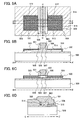
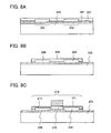
- FIGS. 1A to 1C are cross-sectional views illustrating structures of a transistor included in a semiconductor device of the present invention
- FIG. 2A is a top view illustrating a structure of a transistor included in a semiconductor device of the present invention and FIGS. 2B and 2C are cross-sectional views illustrating the same
- FIG. 3A is a top view illustrating a structure of a transistor included in a semiconductor device of the present invention and FIGS. 3B and 3C are cross-sectional views illustrating the same
- FIG. 4A is a top view illustrating a structure of a transistor included in a semiconductor device of the present invention and FIGS. 4B and 4C are cross-sectional views illustrating the same
- FIGS. 5A is a top view illustrating a structure of a transistor included in a semiconductor device of the present invention and FIGS. 5B and 5C are cross-sectional views illustrating the same;
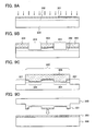
- FIGS. 6A to 6D are views illustrating a manufacturing method of a semiconductor device of the present invention;
- FIGS. 7A to 7D are views illustrating a manufacturing method of a semiconductor device of the present invention;
- FIGS. 8A to 8C are views illustrating a manufacturing method of a semiconductor device of the present invention;
- FIGS. 9A to 9D are views illustrating a manufacturing method of a semiconductor device of the present invention;
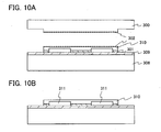
- FIGS. 10A and 10B are views illustrating a manufacturing method of a semiconductor device of the present invention;
- FIGS. 11A to 11D are views illustrating a manufacturing method of a semiconductor device of the present invention
- FIGS. 12A to 12C are views illustrating a manufacturing method of a semiconductor device of the present invention
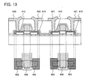
- FIG. 13 is a view illustrating a manufacturing method of a semiconductor device of the present invention
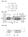
- FIGS. 14A to 14C are views illustrating a structure of an inverter included in a semiconductor device of the present invention
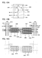
- FIGS. 15A to 15C are views illustrating a structure of a NAND included in a semiconductor device of the present invention
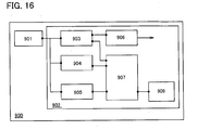
- FIG. 16 is a diagram showing a structure of an RF tag which is one of semiconductor devices of the present invention
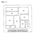
- FIG. 17 is a diagram showing a structure of a CPU which is one of semiconductor devices of the present invention
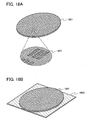
- FIGS. 18A and 18B are diagrams showing a manufacturing method of a semiconductor device of the present invention
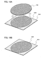
- FIGS. 19A and 19B are diagrams showing a manufacturing method of a semiconductor device of the present invention
- FIG. 20 is a diagram showing a manufacturing method of a semiconductor device of the present invention
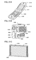
- FIGS. 21A to 21C are diagrams of electronic devices in each of which a semiconductor device of the present invention is used.
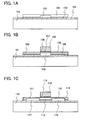
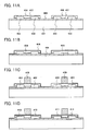
- FIG. 1A A structure of a semiconductor film included in a semiconductor element in a semiconductor device of the present invention will be described with reference to FIG. 1A .
- a semiconductor film 100 shown in FIG. 1A is formed over a flat base substrate 101.
- the semiconductor film 100 has a recess on the base substrate 101 side, and the recess forms a cavity 102 between the semiconductor film 100 and the base substrate 101.
- the position and the number of the cavity 102 is not limited to the structure shown in FIG. 1A .
- One cavity 102 or a plurality of cavities 102 may be provided between the semiconductor film 100 and the base substrate 101.
- an insulating film 103 is formed between the semiconductor film 100 and the base substrate 101 except the region where the cavity 102 is formed. Further, an insulating film 104 is also formed between the insulating film 103 and the base substrate 101. When the insulating film 103 is attached to the insulating film 104; thus, the semiconductor film 100 and the base substrate 101 can be bonded to each other.
- the insulating film 103 may be formed of one insulating film or may be formed such that a plurality of insulating films is stacked.
- the insulating film 104 may be formed of one insulating film or may be formed such that a plurality of insulating films is stacked.
- the insulating film 104 may be formed over the entire surface of the base substrate 101 or may be partially formed such that the insulating film 104 covers at least a region which overlaps with the insulating film 103.
- the semiconductor film 100 and the base substrate 101 are bonded to each other using the insulating film 103 and the insulating film 104; however, the present invention is not limited to the structure. It is not necessary to provide both the insulating film 103 and the insulating film 104, and either one of them may be provided instead.
- the insulating film 104 of the insulating film 103 and the insulating film 104 is formed, the insulating film 104 and the semiconductor film 100 can be attached and thereby the base substrate 101 and the semiconductor film 100 can be bonded to each other.
- the base substrate 101 and the semiconductor film 100 can be bonded by attaching the insulating film 103 and the base substrate 101 together.
- FIG. 1B shows an example of a cross-sectional view of the transistor formed using the semiconductor film 100.
- the transistor shown in FIG. 1B includes the semiconductor film 100 in which a pair of impurity regions 105 and 106, one of which functions as a source and the other as a drain, and a channel formation region 107 are included.
- the transistor shown in FIG. 1B includes an electrode 109 which functions as a gate so that the electrode 109 overlaps with the channel formation region 107 with a gate insulating film 108 interposed therebetween.
- a cavity 102 is provided at a position overlapping with the channel formation region 107 and an electrode 109.
- the position of the cavity is not limited to the structure shown in FIG. 1B .
- the cavity may be formed so as to overlap with one of the pair of impurity regions 105 and 106, or may be formed so as to overlap with the pair of impurity regions 105 and 106 and the channel formation region 107. Self-heating can be suppressed more in the case where the cavity is formed so as to overlap with at least the channel formation region 107 than in the case where the cavity is formed so as to overlap with only the impurity regions 105 and 106.
- FIG. 1C shows an example of a cross-sectional view of a transistor which is formed using the semiconductor film 110 which has two recesses.
- the transistor shown in FIG. 1C includes the semiconductor film 110 in which a pair of impurity regions 111 and 112, one of which functions as a source and the other as a drain, and a channel formation region 113 are included.
- the transistor shown in FIG. 1C includes an electrode 115 which functions as a gate so that the electrode 115 overlaps with the channel formation region 113 with a gate insulating film 114 interposed therebetween.
- the transistor shown in FIG. 1C includes cavities 117 and 118 which are formed with the recesses, between the semiconductor film 110 and a base substrate 116.
- the cavities 117 and 118 are formed at positions overlapping with the pair of impurity regions 111 and 112, respectively.
- Junction capacitance of the transistor can be reduced more in the case where the cavities 117 and 118 overlap with at least the impurity regions 111 and 112, respectively, than in the case where a cavity which overlaps with only the channel formation region 113 is formed.
- the cavity 102 is included between the semiconductor film 100 and the base substrate 101, and the semiconductor film 100 is in contact with the cavity 102.
- the cavities 117 and 118 are included between the semiconductor film 110 and the base substrate 116, and the semiconductor film 110 is in contact with the cavities 117 and 118.
- the cavities 102, 117, and 118 are filled with air, nitrogen, an inert gas, or the like that has lower relative permittivity than an inorganic insulating film of silicon oxide or the like, whereby parasitic capacitance or junction capacitance of the transistor can be reduced.
- a natural oxide film is formed, in some cases, in a portion of the semiconductor film 100, which is in contact with the cavity 102 and a portion of the semiconductor film 110, which is in contact with the cavities 117 and 118.
- an insulating film described in Patent Document 2 is supposed to have a thickness of several ⁇ m to several hundreds ⁇ m, and the natural oxide film is about several nm thick, which is remarkably thinner than the insulating film.
- parasitic capacitance or junction capacitance of the transistor can be reduced more in the present invention than in the case where the insulating film is formed to the above-described thickness in the portion of the semiconductor film 100, which is in contact with the cavity 102 and the portion of the semiconductor film 110, which is in contact with the cavities 117 and 118.
- the cavities 102, 117, and 118 are filled with gas is described in this embodiment mode, the present invention is not limited to this structure.
- the cavities 102, 117, and 118 may be filled with a material other than gas that has lower relative permittivity than an inorganic insulating film of silicon oxide or the like, for example, a porous insulating film (a porous material) including a large number of pores therein.
- the semiconductor display devices include the following in its category: liquid crystal display devices, light-emitting devices in which a light-emitting element typified by an organic light-emitting element (OLED) is provided for each pixel, DMDs (digital micromirror devices), PDPs (plasma display panels), FEDs (field emission displays), or other display devices in which a circuit element using a semiconductor film is included in a driver circuit.
- OLED organic light-emitting element
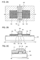
- FIG. 2A shows an example of a top view of a transistor included in a semiconductor device of the present invention and FIGS. 2B and 2C each show an example of a cross-sectional view thereof.
- FIG. 2A is a top view of the transistor
- FIG. 2B is a cross-sectional view taken along line A-A' in FIG. 2A
- FIG. 2C is a cross-sectional view taken along line B-B' in FIG. 2A .
- the transistor shown in FIGS. 2A to 2C includes a semiconductor film 120 functioning as an active layer, an electrode 121, a portion of which overlapping with the semiconductor film 120 functions as a gate, and a gate insulating film 122 provided between the semiconductor film 120 and the electrode 121.
- the semiconductor film 120 includes impurity regions 123 and 124, one of which functions as a source and the other as a drain, a channel formation region 125, and LDD (lightly doped drain) regions 126 and 127 provided respectively between the impurity region 123 and the channel formation region 125 and between the impurity region 124 and the channel formation region 125.
- a cavity 130 is provided between the semiconductor film 120 and the base substrate 129.
- the cavity 130 is provided inside a region which overlaps with the semiconductor film 120. Further, the cavity 130 overlaps with the channel formation region 125 in the semiconductor film 120. Self-heating can be suppressed more in the case where the cavity is formed so as to overlap with at least the channel formation region 125 than in the case where the cavity is formed so as to overlap with only the impurity regions 123 and 124.
- the semiconductor film 120 of the transistor shown in FIGS. 2A to 2C includes the LDD regions 126 and 127
- the present invention is not limited to this structure.
- the LDD regions 126 and 127 are not necessarily provided, or either one of the LDD region 126 or the LDD region 127 may be provided.
- the LDD regions 126 and 127 are provided in regions other than the region in the semiconductor film 120, which overlaps with the electrode 121
- the present invention is not limited to this structure.
- the LDD regions 126 and 127 may be provided in regions overlapping with the electrode 121.
- the LDD regions 126 and 127 may be provided so as to extend to the region overlapping with the electrode 121 and a region other than the aforementioned region.
- a sidewall 128 which is used as a mask when the LDD regions 126 and 127 are formed is provided on sides of the electrode 121 in the transistor shown in FIGS. 2A to 2C , the present invention is not limited to this structure.
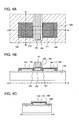
- FIG. 3A shows an example of a top view of a transistor included in a semiconductor device of the present invention and FIGS. 3B and 3C each show an example of a cross-sectional view thereof.
- FIG. 3A is a top view of the transistor
- FIG. 3B is a cross-sectional view taken along line A-A' in FIG. 3A
- FIG. 3C is a cross-sectional view taken along line B-B' in FIG. 3A .
- the transistor shown in FIGS. 3A to 3C includes a semiconductor film 140 functioning as an active layer, an electrode 141, a portion of which overlapping with the semiconductor film 140 functions as a gate, and a gate insulating film 142 provided between the semiconductor film 140 and the electrode 141.
- the semiconductor film 140 includes impurity regions 143 and 144, one of which functions as a source and the other as a drain, a channel formation region 145, and LDD (lightly doped drain) regions 146 and 147 provided respectively between the impurity region 143 and the channel formation region 145 and between the impurity region 144 and the channel formation region 145.
- a cavity 150 is provided between the semiconductor film 140 and a base substrate 149.
- the cavity 150 is not fit into a region which overlaps with the semiconductor film 140, but it extends to end portions of the semiconductor film 140. Therefore, unlike the transistor shown in FIGS. 2A and 2B , a recess extends to end portions of the semiconductor film 140; namely, the cavity 150 opens at end portions of the semiconductor film 140. Further, the cavity 150 overlaps with the channel formation region 145 in the semiconductor film 140. In the case where the cavity overlaps with at least the channel formation region 145, self-heating can be further suppressed in comparison with the case of forming the cavity so as to overlap with only the impurity regions 143 and 144. Further, since the cavity 150 opens at end portions of the semiconductor film 140, difference in air pressure between the inside and the outside of the cavity 150 can be reduced. Accordingly, even if the temperature rapidly changes in heat treatment, the semiconductor film 140 can be prevented from being deformed.
- the semiconductor film 140 of the transistor shown in FIGS. 3A to 3C includes the LDD regions 146 and 147
- the present invention is not limited to this structure.
- the LDD regions 146 and 147 are not necessarily provided, or either one of the LDD region 146 or the LDD region 147 may be provided.
- the LDD regions 146 and 147 are provided in regions other than the region in the semiconductor film 140, which overlaps with the electrode 141
- the present invention is not limited to this structure.
- the LDD regions 146 and 147 may be provided in regions overlapping with the electrode 141.
- the LDD regions 146 and 147 may be provided so as to extend to the region overlapping with the electrode 141 and a region other than the aforementioned region.
- a sidewall 148 which is used as a mask when the LDD regions 146 and 147 are formed is provided on sides of the electrode 141 in the transistor shown in FIGS. 3A and 3B , the present invention is not limited to this structure.
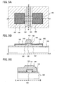
- FIG. 4A shows an example of a top view of a transistor included in a semiconductor device of the present invention and FIGS. 4B and 4C each show an example of a cross-sectional view thereof.
- FIG. 4A is a top view of the transistor
- FIG. 4B is a cross-sectional view taken along line A-A' in FIG. 4A
- FIG. 4C is a cross-sectional view taken along line B-B' in FIG. 4A .
- the transistor shown in FIGS. 4A to 4C includes a semiconductor film 160 functioning as an active layer, an electrode 161, a portion of which overlapping with the semiconductor film 160 functions as a gate, and a gate insulating film 162 provided between the semiconductor film 160 and the electrode 161.
- the semiconductor film 160 includes impurity regions 163 and 164, one of which functions as a source and the other as a drain, a channel formation region 165, and LDD (lightly doped drain) regions 166 and 167 provided respectively between the impurity region 163 and the channel formation region 165 and between the impurity region 164 and the channel formation region 165.
- Two cavities of a cavity 170 and a cavity 171 are provided between the semiconductor film 160 and the base substrate 169.
- the cavity 170 and the cavity 171 overlap with the impurity region 163 and the impurity region 164, respectively.
- the cavity 170 and the cavity 171 may be fit into a region which overlaps with the semiconductor film 160, or may be extended to end portions of the semiconductor film 160 without being fit thereinto, and thereby the recesses may be open at the end portions of the semiconductor film 160.
- junction capacitance of the transistor can be further reduced in comparison with the case of forming cavities which overlap with only the channel formation region 165.
- the cavities 170 and 171 extend to end portions of the semiconductor film 160, the cavities 170 and 171 open at end portions of the semiconductor film 160; therefore, difference in air pressure between the inside and the outside of the cavities 170 and 171 can be reduced. Accordingly, even if the temperature rapidly changes in heat treatment, the semiconductor film 160 can be prevented from being deformed.
- the semiconductor film 160 of the transistor shown in FIGS. 4A to 4C includes the LDD regions 166 and the LDD region 167
- the present invention is not limited to this structure.
- the LDD regions 166 and the LDD region 167 are not necessarily provided, or either one of the LDD region 166 or the LDD region 167 may be provided.
- the LDD regions 166 and 167 are provided in regions other than the region overlapping with the electrode 161 in the semiconductor film 160
- the present invention is not limited to this structure.
- the LDD regions 166 and 167 may be provided in regions overlapping with the electrode 161.
- the LDD regions 166 and 167 may be provided so as to extend to the region overlapping with the electrode 161 and a region other than the aforementioned region.
- a sidewall 168 which is used as a mask when the LDD regions 166 and 167 are formed is provided on sides of the electrode 161 in the transistor shown in FIGS. 4A and 4B , the present invention is not limited to this structure.
- FIG. 5A shows an example of a top view of a transistor included in a semiconductor device of the present invention
- FIGS. 5B and 5C each show an example of a cross-sectional view thereof.
- FIG. 5A is a top view of the transistor
- FIG. 5B is a cross-sectional view taken along line A-A' in FIG. 5A
- FIG. 5C is a cross-sectional view taken along line B-B' in FIG. 5A .
- the transistor shown in FIGS. 5A to 5C includes a semiconductor film 180 functioning as an active layer, an electrode 181, a portion of which overlapping with the semiconductor film 180 functions as a gate, and a gate insulating film 182 provided between the semiconductor film 180 and the electrode 181.
- the semiconductor film 180 includes impurity regions 183 and 184, one of which functions as a source and the other as a drain, a channel formation region 185, and LDD (lightly doped drain) regions 186 and 187 provided respectively between the impurity region 183 and the channel formation region 185 and between the impurity region 184 and the channel formation region 185.
- a cavity 190 is provided between the semiconductor film 180 and a base substrate 189.
- the cavity 190 overlap with the impurity regions 183 and 184 and the channel formation region 185.
- the cavity 190 may be fit into a region which overlaps with the semiconductor film 180, or may be extended to end portions of the semiconductor film 180 without being fixed thereinto, and thereby the recesses may be open at the end portions of the semiconductor film 180.
- the cavity 190 overlaps with the impurity regions 183 and 184 and the channel formation region 185, not only can self-heating be suppressed but also junction capacitance of the transistor can be further reduced.
- the cavity 190 when the cavity 190 extends to end portions of the semiconductor film 180, the cavity 190 opens at end portions of the semiconductor film 180; therefore, difference in air pressure between the inside and the outside of the cavity 190 can be reduced. Accordingly, even if the temperature rapidly changes in heat treatment, the semiconductor film 180 can be prevented from being deformed.
- the semiconductor film 180 of the transistor shown in FIGS. 5A to 5C includes the LDD regions 186 and 187
- the present invention is not limited to this structure.
- the LDD regions 186 and 187 are not necessarily provided, or either one of the LDD region 186 or the LDD region 187 may be provided.
- the LDD regions 186 and 187 are provided in regions other than the region overlapping with the electrode 181 in the semiconductor film 180
- the present invention is not limited to this structure.
- the LDD regions 186 and 187 may be provided in regions overlapping with the electrode 181.
- the LDD regions 186 and 187 may be provided so as to extend to the region overlapping with the electrode 181 and a region other than the aforementioned region.
- a sidewall 188 which is used as a mask when the LDD regions 186 and 187 are formed is provided on sides of the electrode 181 in the transistor shown in FIGS. 5A and 5B , the present invention is not limited to this structure.
- FIG. 6A shows an example of a top view of a transistor included in a semiconductor device of the present invention and FIGS. 6B and 6C each show an example of a cross-sectional view thereof.
- FIG. 6A is a top view of the transistor
- FIG. 6B is a cross-sectional view taken along line A-A' in FIG. 6A
- FIG. 6C is a cross-sectional view taken along line B-B' in FIG. 6A
- FIG. 6D is a cross-sectional view taken along line C-C' in FIG. 6A .
- the transistor shown in FIGS. 6A to 6C includes a semiconductor film 500 functioning as an active layer, an electrode 501, a portion of which overlapping with the semiconductor film 500 functions as a gate, and a gate insulating film 502 provided between the semiconductor film 500 and the electrode 501.
- the semiconductor film 500 includes impurity regions 503 and 504, one of which functions as a source and the other as a drain, a channel formation region 505, and LDD (lightly doped drain) regions 506 and 507 provided respectively between the impurity region 503 and the channel formation region 505 and between the impurity region 504 and the channel formation region 505.
- a plurality of cavities 510 to 515 are provided between the semiconductor film 500 and a base substrate 509.
- the cavities 510 and 511 overlap with the impurity region 503 and the cavities 512 and 513 overlap with the impurity region 504.
- the cavities 514 and 515 overlap with the impurity regions 503 and 504 and the channel formation region 505. Since the cavities 510 to 513 overlap with the impurity regions 503 and 504, self-heating can be reduced. Further, the cavities 514 and 515 overlap with the impurity region 503 and 504 and the channel formation region 505; thus, not only can self-heating be suppressed but also junction capacitance of the transistor can be further reduced.
- the cavities 510 to 515 may be fit into a region which overlaps with the semiconductor film 500, or may be extended to end portions of the semiconductor film 500 without being fit thereinto, and thereby the recesses may be open at the end portions of the semiconductor film 500.
- the cavities 510 to 515 extend to end portions of the semiconductor film 500, the cavities 510 to 515 open at end portions of the semiconductor film 500; therefore, difference in air pressure between the inside and the outside of the cavities 510 to 515 can be reduced. Accordingly, even if the temperature rapidly changes in heat treatment, the semiconductor film 500 can be prevented from being deformed.
- the semiconductor film 500 of the transistor shown in FIGS. 6A to 6D includes the LDD regions 506 and the LDD region 507
- the present invention is not limited to this structure.
- the LDD regions 506 and the LDD region 507 are not necessarily provided, or either one of the LDD region 506 or the LDD region 507 may be provided.
- the LDD regions 506 and 507 are provided in regions other than the region overlapping with the electrode 501 in the semiconductor film 500, the present invention is not limited to this structure.
- the LDD regions 506 and 507 may be provided in regions overlapping with the electrode 501.
- the LDD regions 506 and 507 may be provided so as to extend to the region overlapping with the electrode 501 and a region other than the aforementioned region.
- a sidewall 508 which is used as a mask when the LDD regions 506 and 507 are formed is provided on sides of the electrode 501 in the transistor shown in FIGS. 6A to 6B , the present invention is not limited to this structure.
- the cavity can be formed so as to have a larger area under the semiconductor film, and thus junction capacitance and parasitic capacitance can be reduced more and self-heating can be suppressed more in the case where a plurality of cavities is provided.
- a transistor with higher physical strength than a transistor in the case where one cavity is provided can be formed.
- a plurality of cavities may be provided so as to overlap with the channel formation region.
- the cavity can be formed so as to have a larger area under the channel formation region, and thus self-heating can be suppressed more than in the case where a plurality of cavities is provided under the channel formation region.
- a transistor with higher physical strength than a transistor in the case where one cavity is provided can be formed.
- the present invention is not limited to this structure.
- a plurality of cavities which overlap with one impurity region may be provided.
- the cavity can be formed so as to have a larger area under the impurity region, and thus self-heating can be suppressed more than in the case where a plurality of cavities is provided.
- a transistor with higher physical strength than a transistor in the case where one cavity is provided can be formed.
- This embodiment can be implemented in combination with any of the embodiment modes as appropriate.
- a manufatcuring method of a semiconductor device of the present invention in which a semiconductor film is transferred from a semiconductor substrate (a bond substrate) to a supporting substrate (a base substrate) having been processed tinto a desired shape is formed will be described.
- a bond substrate 200 on which an insulating film 201 is formed is prepared.
- the insulating film 201 is formed using an insulating material such as silicon oxide, silicon nitride oxide, or silicon nitride. Since the thickness of the insulating film 201 influences the depth of a defect layer 202 which is to be formed later, the thickness of the insulating film 201 is desirably uniform.
- the insulating film 201 is desirably formed by thermal oxidation of the bond substrate 200.
- the insulating film 201 is preferably formed by heat treatment at 900 °C to 1100 °C in a water vapor atmosphere.
- the insulating film 201 may be formed by oxidation of the bond substrate 200 with oxygen plasma treatment.
- the insulating film 201 can be formed using a mixed gas of silane and oxygen, a mixed gas of TEOS (tetraethoxysilane) and oxygen, or the like by a vapor deposition method such as thermal CVD, plasma CVD, atmospheric pressure CVD, or bias ECRCVD.
- a surface of the insulating film 201 may be densified with oxygen plasma treatment.
- the insulating film 201 may be formed using silicon oxide which is formed with the use of an organic silane gas by a chemical vapor deposition method.
- silane gas the following may be used: a silicon-containing compound such as ethyl silicate (TEOS: Si(OC 2 H 5 ) 4 ), tetramethylsilane (TMS: Si(CH 3 ) 4 ), tetramethylcyclotetrasiloxane (TMCTS), octamethylcyclotetrasiloxane (OMCTS), hexamethyldisilazane (HMDS), triethoxysilane (SiH(OC 2 H 5 ) 3 ), or trisdimethyaminosilane (SiH(N(CH 3 ) 2 ) 3 ).
- TEOS ethyl silicate
- TMS tetramethylsilane
- TCS tetramethylcyclotetrasiloxane
- OCTS octamethylcycl
- the insulating film 201 may be a single-layer insulating film or a layer in which a plurality of insulating films is stacked.
- the insulating film 201 is used in which, from the bond substrate 200 side, silicon oxynitride in which the amount of oxygen is higher than that of nitrogen, silicon nitride oxide in which the amount of nitrogen is higher than that of oxygen, and silicon oxide formed using an organic silane gas by a chemical vapor deposition method are stacked.
- the insulating film 201 can be formed using a mixed gas of silane and ammonium by a vapor deposition method such as plasma CVD.
- a vapor deposition method such as plasma CVD.
- the insulating film 201 can be formed using a mixed gas of silane and ammonium or a mixed gas of silane and nitrogen oxide by a vapor deposition method such as plasma CVD.
- a step of removing the semiconductor film from the bond substrate 200 hydrogen or a noble gas, or hydrogen ions or noble gas ions is introduced into the bond substrate 200 at high concentration, and accordingly a surface of the bond substrate 200 becomes rough and sufficient bond strength for attachment with the base substrate cannot be obtained.
- the insulating film 201 is provided, whereby the surface of the bond substrate 200 is protected at the time of the introduction of hydrogen or a noble gas, or hydrogen ions or noble gas ions, and the base substrate and the bond substrate 200 can be firmly attached to each other.
- the defect layer 202 having very small voids is formed in a region at a certain depth from a surface of the bond substrate 200.
- the position where the defect layer 202 is formed is determined depending on acceleration voltage at the time of the above-described introduction.
- the thickness of a semiconductor film 207 which is transferred from the bond substrate 200 to the base substrate is determined by the position of the defect layer 202; therefore, acceleration of the voltage at the time of the introduction is performed in consideration of the thickness of the semiconductor film.
- the semiconductor film 207 is formed to a thickness of 10 nm to 200 nm, preferably 10 nm to 50 nm.
- the dose is desirably 1 ⁇ 10 16 /cm 2 to 1 ⁇ 10 17 /cm 2 .
- an insulating film 201 formed over the bond substrate 200 is processed (patterned) into a desired shape, and thereby the insulating film 201 is partially removed to form recesses 204.
- the recesses 204 are formed in the region in bond substrate 200, where the insulating film 201 is partially removed. Specifically, patterning can be performed in such a manner that the bond substrate 200 and the insulating film 201 are etched using a mask 203 formed of resist.
- the recesses 204 correspond to cavities which are to be formed between a semiconductor film of a transistor and a base substrate. Therefore, the recesses 204 are formed in consideration of the shape of the semiconductor film of the transistor.
- the recesses 204 are formed to have a depth such that the recesses are above the position where the defect layer 202 is formed.
- the bond substrate 200 may be processed (patterned) into a desired shape using an inorganic insulating film as a hard mask instead of using a resist.
- the etching may be performed using a dry etching method, for example, reactive ion etching (RIE), ICP (Inductively Coupled Plasma) etching, ECR (Electron Cyclotron Resonance) etching, parallel plate (Capacitive Coupled Plasma) etching, magnetron plasma etching, dual-frequency plasma etching, helicon wave plasma etching, or the like.
- RIE reactive ion etching
- ICP Inductively Coupled Plasma
- ECR Electrode
- Parallel plate Capacitive Coupled Plasma
- magnetron plasma etching dual-frequency plasma etching
- helicon wave plasma etching or the like.
- etching may be performed under the following conditions: the flow rate of chlorine, which is an etching gas: 40 sccm to 100 sccm; power applied to a coil electrode: 100 W to 200 W; the temperature of a lower electrode (on the bias side): 40 W to 100 W; and the reaction pressure: 0.5 Pa to 1.0 Pa.
- the flow rate of chlorine which is an etching gas: 40 sccm to 100 sccm
- power applied to a coil electrode 100 W to 200 W
- the temperature of a lower electrode (on the bias side) 40 W to 100 W
- the reaction pressure 0.5 Pa to 1.0 Pa.
- etching is performed under the following conditions: the flow rate of chlorine, which is an etching gas: 100 sccm, the reaction pressure: 1.0 Pa, the temperature of the lower electrode: 70 °C, RF (13.56 MHz) power applied to the coil electrode: 150 W, power applied to the lower electrode (on the bias side): 40 W, and thereby recesses 204 are formed to have a depth of approximately 5 nm to 190 nm, preferably 20 nm to 150 nm in the bond substrate 200.
- a chloride gas such as chlorine, boron chloride, silicon chloride or carbon tetrachloride
- a fluoride gas such as carbon tetrafluoride, sulfur fluoride, or nitrogen fluoride
- oxygen is used as appropriate.
- etching may be performed in addition to the above etching under conditions such that damage on the bond substrate 200 can be reduced.
- the etching is performed by approximately several nm under the conditions: the flow rate of chlorine, which is an etching gas 100 sccm, reaction pressure 0.67 Pa, the temperature of a lower electrode: 0 °C; RF (13.56 MHz) power applied to a coiled electrode: 2000 W; power applied to the lower electrode (on the bias side): 0 W; and etching time: 30 seconds.
- the etching gas used for the etching is not limited to chlorine, and for example, water, hydrogen, ammonia, or the like may be used.
- Plasma damage inflicted on the recesses 204 which are formed in the bond substrate 200 can be repaired by the etching. Repairing of the plasma damage makes it possible to reduce decrease in the lifetime of carriers, and to reduce leakage current of the transistor in an off-state, namely, to improve off properties. Further, the threshold voltage of the transistor can be prevented from being deviated due to plasma.
- wet etching can be used to form the recesses 204.
- the insulating film 201 is formed of silicon oxide, silicon oxynitride, or silicon nitride oxide
- etching is performed partially using aqueous hydrofluoric acid.
- the recesses 204 may be formed by partially etching the bond substrate 200 using a tetraethylammonium hydroxide (tetramethylammonium hydroxide, abbreviated to TMAH) solution.
- TMAH tetraethylammonium hydroxide
- the bond substrate 200 may be hydrogenated.
- the hydrogenation is performed for example, at 350 °C in a hydrogen atmosphere for approximately two hours.
- the bond substrate 200 provided with the recesses 204 is bonded to the base substrate 205.
- the bond substrate 200 and the base substrate 205 are bonded so that the recesses 204 open toward the bond substrate 200.
- An insulating film 206 is formed on the surface of the base substrate 205 in order to improve the bond strength between the bond substrate 200 and the base substrate 205.
- the insulating film 206 so that the insulating film 201 formed on the bond substrate 200 and the insulating film 206 are attached to one another, and thereby the bond substrate 200 and the base substrate 205 are bonded to each other.
- the bond substrate 200 and the base substrate 205 are bonded to each other by van der Waals forces, so that they are firmly attached to each other at room temperature.
- various substrates can be used for the base substrate 205.
- a substrate such as a quartz substrate or a sapphire substrate can be used as well as a glass substrate made of aluminosilicate glass, barium borosilicate glass, aluminoborosilicate glass, or the like.
- a semiconductor substrate formed of silicon, gallium arsenide, indium phosphide, or the like can be used.
- a single crystal semiconductor substrate of silicon, germanium, or the like or a polycrystalline semiconductor substrate of silicon, germanium, or the like can be used.
- a single crystal semiconductor substrate or a polycrystalline semiconductor substrate formed of a compound semiconductor such as gallium arsenide or indium phosphide can be used as the bond substrate 200.
- a semiconductor substrate formed of silicon having lattice distortion, silicon germanium in which germanium is added to silicon, or the like may also be used. Silicon having lattice distortion can be formed by formation of silicon on silicon germanium or silicon nitride which has larger lattice constant than silicon.
- heat treatment or pressure treatment may be performed after the base substrate 205 and the bond substrate 200 are bonded to each other.
- the bond strength can be increased with heat treatment or pressure treatment.
- the insulating film 206 can be formed using silicon oxide or silicon nitride oxide.
- silicon nitride oxide desirably contains more carbon than oxygen, specifically, it desirably contains oxygen at 55 atomic% to 65 atomic%, nitrogen at 1 atomic% to 20 atomic%, silicon at 25 atomic% to 35 atomic%, and hydrogen at 0.1 atomic% to 10 atomic%.
- the insulating film 206 can be formed by thermally oxidizing the base substrate 205.
- a silicon nitride film may be provided between the insulating film 206 and the base substrate 205.
- an alkali metal such as sodium or an alkaline earth metal is diffused into the bond substrate 200, thereby precluding adverse effects on characteristics of semiconductor elements such as a transistor, which are to be formed later.
- a silicon nitride oxide film containing nitrogen than oxygen which has composition containing oxygen at 15 atomic% to 30 atomic%, nitrogen at 20 atomic% to 35 atomic%, silicon at 25 atomic% to 35 atomic%, and hydrogen at 15 atomic% to 25 atomic%.
- aluminum nitride, aluminum nitride oxide or the like may be used to prevent diffusion of impurities.
- Heat treatment is performed after the bond substrate 200 and the base substrate 205 are attached to each other, and thereby the adjacent microvoids in the defect layer 202 are coupled, and the volume of the microvoid is increased. As a result, as shown in FIG. 7D , the bond substrate 200 is split along the defect layer 202; thus, the insulating film 201 and the semiconductor film 207 which has been part of the bond substrate 200 are separated from the bond substrate 200.
- the heat treatment is preferably performed at a temperature that is equal to or lower than the allowable temperature limit of the bond substrate 200. For example, heat treatment may be performed at a temperature ranging from 400 °C to 600 °C. After the separation, the semiconductor film 207 and the insulating film 201 are transferred to the base substrate 205. After that, heat treatment at a temperature ranging from 400 °C to 600 °C is preferably performed in order to make stronger the attachment between the insulating film 201 and the insulating film 206.
- Crystal plane orientation of the semiconductor film 207 can be controlled with the plane orientation of the bond substrate 200.
- the bond substrate 200 having crystal plane orientation which is suitable for a semiconductor element which is to be formed may be selected as appropriate.
- the mobility of the transistor depends on the crystal plane orientation of the semiconductor film 207. In order to obtain a transistor with higher mobility, the direction of bonding the bond substrate 200 is set in consideration of the direction of a channel and the crystal plane orientation.
- a surface of the transferred semiconductor film 207 is planarized.
- the planarization is not necessarily essential, the planarization makes it possible to improve characteristics of the interface between the semiconductor film 207 and a gate insulating film in the transistor which is to be formed later.
- the planarization can be performed by chemical mechanical polishing (CMP), liquid jet polishing, or the like.
- CMP chemical mechanical polishing
- the thickness of the semiconductor film 207 is reduced by the above-described planarization.
- the semiconductor film 207 may be bonded to the base substrate 205 by another bonding method such as ELTRAN (epitaxial layer transfer), a dielectric isolation method, or a PACE (plasma assisted chemical etching) method.
- ELTRAN epitaxial layer transfer
- dielectric isolation method dielectric isolation method
- PACE plasma assisted chemical etching
- the semiconductor film 207 is patterned, whereby an island-shaped semiconductor film 208 is formed.
- the patterning of the insulating film 201 may be performed using the mask used for patterning the semiconductor film 207.
- a pair of cavities 209 formed by the recesses 204 is provided between the island-shaped semiconductor film 208 and the base substrate 205.
- the present invention makes it possible to form various semiconductor elements such as transistors with the use of the semiconductor film 208 which is formed through the above-described steps.
- a transistor 210 formed using the semiconductor film 208 is shown in FIG. 8C as an example.
- the recesses 204 are formed by etching; thus, the cavities 209 with a desired depth and a desired shape can be formed precisely through a simple procedure.
- the cavities 209 are included between the semiconductor film 208 and the base substrate 205, and the cavities 209 are in contact with the semiconductor film 208.
- the cavities 209 are filled with air, nitrogen, an inert gas, or the like that has lower relative permittivity than an inorganic insulating film of silicon oxide or the like, parasitic capacitance or junction capacitance of the transistor 210 can be reduced. It is desirable that the percentage of moisture contained in the above-described gas be decreased in order to suppress volume expansion with temperature change. Note that, in fact, a natural oxide film is formed, in some cases, in a portion of the semiconductor film 208, which is in contact with the cavities 209.
- the insulating film described in Patent Document 2 is supposed to have a thickness of several ⁇ m to several hundreds ⁇ m, and the natural oxide film is about several nm thick, which is remarkably thinner than the insulating film.
- parasitic capacitance or junction capacitance of the transistor 210 can be reduced more in the present invention than in the case where the insulating film is formed to the above-described thickness in the portion of the semiconductor film 208, which is in contact with the cavities.
- the cavities 209 are filled with gas such as air
- gas such as air
- the present invention is not limited to this structure.
- the cavities 209 may be filled with a material other than gas that has lower relative permittivity than an inorganic insulating film of silicon oxide or the like, for example, a porous insulating film (a porous material) including a large number of pores therein.
- the present invention is not limited to this structure.
- One cavity 209 may be provided, or three or more cavities 209 may be provided.
- the cavities 209 are formed so as to overlap with impurity regions 211, one of which functions as a source and the other as a drain, the present invention is not limited to this structure.
- the cavity 209 may be formed so as to overlap with a channel formation region 212 in the semiconductor film 208, or the cavity 209 may be formed so as to overlap with a pair of the impurity regions 211 and the channel formation region 212.
- junction capacitance can be reduced more in the case of forming the cavity 209 overlaps with at least the impurity regions 211 than in the case of forming the cavity 209 which overlaps with only the channel formation region 212.
- self-heating can be suppressed more in the case where the cavity 209 which overlaps with at least the channel formation region 212 is formed than in the case where the cavity 209 which overlaps with only the impurity regions 211 is formed.
- This embodiment can be implemented in combination with any of the embodiment modes as appropriate.
- a manufacturing method of a semiconductor device of the present invention in which a semiconductor film in which a region to be an island-shaped semiconductor film later is formed in advance in a semiconductor substrate (a bond substrate) is transferred from the semiconductor substrate (a bond substrate) to a supporting substrate (a base substrate).
- a bond substrate 300 on which an insulating film 301 is formed is prepared.
- the insulating film 301 is formed using an insulating material such as silicon oxide, silicon nitride oxide, or silicon nitride. Since the thickness of the insulating film 301 influences the depth of a defect layer 302 which is to be formed later, the thickness of the insulating film 301 is desirably uniform.
- the insulating film 301 is desirably formed by thermal oxidation of the bond substrate 300.
- the insulating film 301 is preferably formed by heat treatment at 900 °C to 1100 °C in a water vapor atmosphere.
- the insulating film 301 may be formed by oxidizing the bond substrate 300 with oxygen plasma treatment.
- the insulating film 301 can be formed using a mixed gas of silane and oxygen, a mixed gas of TEOS (tetraethoxysilane) and oxygen, or the like by a vapor deposition method such as thermal CVD, plasma CVD, atmospheric pressure CVD, or bias ECRCVD.
- a surface of the insulating film 301 may be densified with oxygen plasma treatment.
- the insulating film 301 may be formed using silicon oxide which is formed with the use of an organic silane gas by a chemical vapor deposition method.
- silane gas the following may be used: a silicon-containing compound such as ethyl silicate (TEOS: Si(OC 2 H 5 ) 4 ), tetramethylsilane (TMS: Si(CH 3 ) 4 ), tetramethylcyclotetrasiloxane (TMCTS), octamethylcyclotetrasiloxane (OMCTS), hexamethyldisilazane (HMDS), triethoxysilane (SiH(OC 2 H 5 ) 3 ), or trisdimethyaminosilane (SiH(N(CH 3 ) 2 ) 3 ).
- TEOS ethyl silicate
- TMS tetramethylsilane
- TCS tetramethylcyclotetrasiloxane
- OCTS octamethylcycl
- the insulating film 301 may be a single-layer insulating film or a layer in which a plurality of insulating films is stacked.
- the insulating film 301 is used in which, from the bond substrate 300 side, silicon oxynitride in which the amount of oxygen is higher than that of nitrogen, silicon nitride oxide in which the amount of nitrogen is higher than that of oxygen, and silicon oxide formed using an organic silane gas by a chemical vapor deposition method are stacked.
- the insulating film 301 can be formed using a mixed gas of silane and ammonium by a vapor deposition method such as plasma CVD.
- the insulating film 301 can be formed using a mixed gas of silane and ammonium or a mixed gas of silane and nitrogen oxide by a vapor deposition method such as plasma CVD.
- a step of removing a semiconductor film from the bond substrate 300 hydrogen ions are introduced into the bond substrate 300 at high dose, and accordingly a surface of the bond substrate 300 becomes rough and sufficient bond strength for attachment with the base substrate would not be obtained.
- the insulating film 301 is provided, so that the surface of the bond substrate 300 is protected at the time of introducing hydrogen ions, and the base substrate and the bond substrate 300 can be firmly attached to each other.
- the defect layer 302 having very small voids is formed in a region at a certain depth from a surface of the bond substrate 300.
- the position where the defect layer 302 is formed is determined depending on acceleration voltage at the time of the above-described introduction.
- the thickness of a semiconductor film 310 which is transferred from the bond substrate 300 to the base substrate is determined by the position of the defect layer 302; therefore, acceleration of the voltage at the time of the introduction is performed in consideration of the thickness of the semiconductor film.
- the semiconductor film 310 is formed to a thickness of 10 nm to 200 nm, preferably 10 nm to 50 nm.
- the dose is desirably 1 ⁇ 10 16 /cm 2 to 1 ⁇ 10 17 /cm 2 .
- an insulating film 301 formed over the bond substrate 300 is processed (patterned) into a desired shape, and thereby the insulating film 301 is partially removed to form recesses 304.
- the recesses 304 are formed in the region in bond substrate 300, where the insulating film 301 is partially removed. Specifically, patterning can be performed in such a manner that the bond substrate 300 and the insulating film 301 are etched using a mask 303 formed of resist.
- the recesses 304 correspond to cavities which are to be formed between a semiconductor film of a transistor and a base substrate. Therefore, the recesses 304 are formed in consideration of the shape of the semiconductor film of the transistor.
- the recesses 304 are formed to have a depth such that the recesses are above the position where the defect layer 302.
- the bond substrate 300 may be processed (patterned) into a desired shape using an inorganic insulating film as a hard mask instead of using a resist.
- the etching may be performed using a dry etching method, for example, reactive ion etching (RIE), ICP (Inductively Coupled Plasma) etching, ECR (Electron Cyclotron Resonance) etching, parallel plate (Capacitive Coupled Plasma) etching, magnetron plasma etching, dual-frequency plasma etching, helicon wave plasma etching, or the like.
- RIE reactive ion etching
- ICP Inductively Coupled Plasma
- ECR Electrode
- Parallel plate Capacitive Coupled Plasma
- magnetron plasma etching dual-frequency plasma etching
- helicon wave plasma etching or the like.
- etching may be performed under the following conditions: the flow rate of chlorine, which is an etching gas: 40 sccm to 100 sccm; power applied to a coil electrode: 100 W to 200 W; the temperature of a lower electrode (on the bias side): 40 W to 100 W; and the reaction pressure: 0.5 Pa to 1.0 Pa.
- the flow rate of chlorine which is an etching gas: 40 sccm to 100 sccm
- power applied to a coil electrode 100 W to 200 W
- the temperature of a lower electrode (on the bias side) 40 W to 100 W
- the reaction pressure 0.5 Pa to 1.0 Pa.
- etching is performed under the following conditions: the flow rate of chlorine, which is an etching gas: 100 sccm, the reaction pressure: 1.0 Pa, the temperature of the lower electrode: 70 °C, RF (13.56 MHz) power applied to the coil electrode: 150 W, power applied to the lower electrode (on the bias side): 40 W, and thereby recesses 304 are formed to have a depth of approximately 5 nm to 190 nm, preferably 20 nm to 150 nm in the bond substrate 300.
- a chloride gas such as chlorine, boron chloride, silicon chloride or carbon tetrachloride
- a fluoride gas such as carbon tetrafluoride, sulfur fluoride, or nitrogen fluoride
- oxygen is used as appropriate.
- etching may be performed in addition to the above etching under conditions such that damage on the bond substrate 300 can be reduced.
- the etching is performed by approximately several nm under the conditions: the flow rate of chlorine, which is an etching gas 100 sccm, reaction pressure 0.67 Pa, the temperature of a lower electrode: 0 °C; RF (13.56 MHz) power applied to a coiled electrode: 2000 W; power applied to the lower electrode (on the bias side): 0 W; and etching time: 30 seconds.
- the etching gas used for the etching is not limited to chlorine, and for example, water, hydrogen, ammonia, or the like may be used.
- Plasma damage inflicted on the recesses 304 which are formed in the bond substrate 300 can be repaired by the etching. Repairing of the plasma damage makes it possible to reduce decrease in the lifetime of carriers, and to reduce leakage current of the transistor in an off-state, namely, to improve off properties. Further, the threshold voltage of the transistor can be prevented from being deviated due to plasma.
- the recesses 304 can be formed by partially etching the bond substrate 300 using a tetraethylammonium hydroxide (tetramethylammonium hydroxide, abbreviated to TMAH) solution.
- TMAH tetraethylammonium hydroxide
- the bond substrate 300 and the insulating film 301 are patterned again, and thereby the insulating film 301 is partially removed and a projection 305 is formed in a region where the insulating film 301 partially remains, over the bond substrate 300.
- patterning can be performed in such a manner that the bond substrate 300 and the insulating film 301 are etched using a mask 306 formed of resist.
- the projection 305 corresponds to a region later to be an island-shaped semiconductor film. Accordingly, the projection 305 is formed in consideration of the shape of the semiconductor film of the transistor. Further, the region in which the projection 305 is formed includes regions where the recesses 304 are formed.
- the recesses 307 other than the projection 305 are formed to have a depth such that the recesses are above the position where the defect layer 302.
- the bond substrate 300 may be processed (patterned) into a desired shape using an inorganic insulating film as a hard mask instead of using a resist.
- the projection 305 is formed after forming the recess 304; however, the recesses 304 may be formed after forming the projection 305.
- the bond substrate 300 may be hydrogenated.
- the hydrogenation is performed for example, at 350 °C in a hydrogen atmosphere for approximately two hours.
- the bond substrate 300 provided with the recesses 304 is bonded to the base substrate 308.
- the bond substrate 300 and the base substrate 308 are bonded so that the recesses 304 and the projection 305 open toward the base substrate 308.
- An insulating film 309 is formed on the surface of the base substrate 308 in order to improve the bond strength between the bond substrate 300 and the base substrate 308.
- the insulating film 309 so that the insulating film 301 formed on the bond substrate 300 and the insulating film 309 bonded, and thereby the bond substrate 300 and the base substrate 308 are attached to each other.
- the bond substrate 300 and the base substrate 308 are attached to each other by van der Waals forces, so that they are firmly attached to each other at room temperature.
- various substrates can be used for the base substrate 308.
- a substrate such as a quartz substrate or a sapphire substrate can be used as well as a glass substrate made of aluminosilicate glass, barium borosilicate glass, aluminoborosilicate glass, or the like.
- a semiconductor substrate formed of silicon, gallium arsenide, indium phosphide, or the like can be used.
- a single crystal semiconductor substrate of silicon, germanium, or the like or a polycrystalline semiconductor substrate of silicon, germanium, or the like can be used.
- a single crystal semiconductor substrate or a polycrystalline semiconductor substrate formed of a compound semiconductor such as gallium arsenide or indium phosphide can be used as the bond substrate 300.
- a semiconductor substrate formed of silicon having lattice distortion, silicon germanium in which germanium is added to silicon, or the like may also be used. Silicon having lattice distortion can be formed by formation of silicon on silicon germanium or silicon nitride which has larger lattice constant than silicon.
- heat treatment or pressure treatment may be performed after the base substrate 308 and the bond substrate 300 are bonded to each other.
- the bond strength can be increased with heat treatment or pressure treatment.
- the insulating film 309 can be formed using silicon oxide or silicon nitride oxide.
- the silicon nitride oxide desirably contains more carbon than oxygen, specifically, it desirably contains oxygen at 55 atomic% to 65 atomic%, nitrogen at 1 atomic% to 20 atomic%, silicon at 25 atomic% to 35 atomic%, and hydrogen at 0.1 atomic% to 10 atomic%.
- the insulating film 309 can be formed by thermally oxidizing the base substrate 308.
- a silicon nitride film may be provided between the insulating film 309 and the base substrate 308.
- an alkali metal such as sodium or an alkaline earth metal is diffused into the bond substrate 300, thereby precluding adverse effects on characteristics of semiconductor elements such as a transistor, which are to be formed later.
- a silicon nitride oxide film containing nitrogen than oxygen which has composition containing oxygen at 15 atomic% to 30 atomic%, nitrogen at 20 atomic% to 35 atomic%, silicon at 25 atomic% to 35 atomic%, and hydrogen at 15 atomic% to 25 atomic%.
- aluminum nitride, aluminum nitride oxide or the like may be used to prevent diffusion of impurities.
- Heat treatment is performed after the bond substrate 300 and the base substrate 308 are attached to each other, and thereby the adjacent microvoids in the defect layer 302 are coupled, and thus the volume of the microvoid is increased.
- the bond substrate 300 is split along the defect layer 302; thus, the semiconductor film 310 and the insulating film 301 which have been part of the bond substrate 300 are separated from the bond substrate 300.
- the heat treatment is preferably performed at a temperature that is equal to or lower than the allowable temperature limit of the bond substrate 300.
- heat treatment may be performed at a temperature ranging from 400 °C to 600 °C.
- the semiconductor film 310 having an island shape and the insulating film 301 are transferred to the base substrate 308.
- heat treatment at a temperature ranging from 400 °C to 600 °C is preferably performed in order to make stronger the attachment between the insulating film 301 and the insulating film 309.
- Crystal plane orientation of the semiconductor film 310 can be controlled with the plane orientation of the bond substrate 300.
- the bond substrate 300 having crystal plane orientation which is suitable for a semiconductor element which is to be formed may be selected as appropriate.
- the mobility of the transistor depends on the crystal plane orientation of the semiconductor film 310. In order to obtain a transistor with higher mobility, the direction of bonding the bond substrate 300 is set in consideration of the direction of a channel and the crystal plane orientation.
- a surface of the transferred semiconductor film 310 is planarized.
- the planarization is not necessarily essential, the planarization makes it possible to improve characteristics of the interface between the semiconductor film 310 and a gate insulating film in the transistor which is to be formed later.
- the planarization can be performed by chemical mechanical polishing (CMP), liquid jet polishing, or the like.
- CMP chemical mechanical polishing
- the thickness of the semiconductor film 310 is reduced by the above-described planarization.
- the semiconductor film 310 may be bonded to the base substrate 308 by another bonding method such as ELTRAN (epitaxial layer transfer), a dielectric isolation method, or a PACE (plasma assisted chemical etching) method.
- ELTRAN epitaxial layer transfer
- dielectric isolation method dielectric isolation method
- PACE plasma assisted chemical etching
- a pair of cavities 311 formed from the recesses 304 is provided between the semiconductor film 310 having an island shape and the base substrate 308.
- the present invention makes it possible to form various semiconductor elements such as transistors with the use of the semiconductor film 310 having an island shape, which is formed through the above-described steps.
- the recesses 304 are formed by etching; thus, the cavities 311 with a desired depth and a desired shape can be formed precisely through a simple procedure.
- the transistor formed using the semiconductor film 310 shown in FIG. 10B has the cavities 311 between the semiconductor film 310 and the base substrate 308, and the cavities 311 are in contact with the semiconductor film 310.
- the cavities 311 are filled with air, nitrogen, an inert gas, or the like that has lower relative permittivity than an inorganic insulating film of silicon oxide or the like, parasitic capacitance or junction capacitance of the transistor can be reduced. It is desirable that the percentage of moisture contained in the above-described gas be decreased in order to suppress volume expansion with temperature change.
- a natural oxide film is formed, in some cases, in a portion of the semiconductor film 310, which is in contact with the cavities 311.
- the insulating film described in Patent Document 2 is supposed to have a thickness of several ⁇ m to several hundreds ⁇ m, and the natural oxide film is about several nm thick, which is remarkably thinner than the insulating film.
- parasitic capacitance or junction capacitance of the transistor can be reduced more in the present invention than in the case where the insulating film is formed to the above-described thickness in the portion of the semiconductor film 310, which is in contact with the cavities.
- the cavities 311 are filled with gas such as air
- gas such as air
- the present invention is not limited to this structure.
- the cavities 311 may be filled with a material other than gas that has lower relative permittivity than an inorganic insulating film of silicon oxide or the like, for example, a porous insulating film (a porous material) including a large number of pores therein.
- the present invention is not limited to this structure.
- One cavity 311 may be provided, or three or more cavities 311 may be provided.
- This embodiment can be implemented in combination with any of the embodiment modes as appropriate.
- an island-shaped semiconductor film 404 and an island-shaped semiconductor film 405 are formed over a base substrate 401 with a pair of cavities 402 and a pair of cavities 403 therebetween, respectively.
- An insulating film 406 formed over the base substrate 401 and an insulating film 407 formed so as to be in contact with the island-shaped semiconductor film 404 and the island-shaped semiconductor film 405 are attached together; thus, the island-shaped semiconductor film 404 and the island-shaped semiconductor film 405 are bonded to the base substrate 401.
- An impurity may be added to the island-shaped semiconductor films 404 and 405 in order to control the threshold voltage.
- boron is preferably added at a concentration of greater than or equal to 5 ⁇ 10 17 cm -3 and less than or equal to 1 ⁇ 10 18 cm -3 .
- the addition of the impurity may be performed before the semiconductor film is transferred to the base substrate 401 or after the transfer.
- Hydrogenation treatment may be performed after the island-shaped semiconductor films 404 and 405 are formed and before a gate insulating film 408 is formed.
- the hydrogenation treatment is performed at 350 °C for about two hours in a hydrogen atmosphere.
- the gate insulating film 408 is formed so as to cover the island-shaped semiconductor films 404 and 405.
- the gate insulating film 408 is formed from a film having a single layer or a layered structure which contain silicon oxide, silicon oxynitride, silicon nitride, hafnium oxide, aluminum oxide, and/or tantalum oxide by plasma CVD, sputtering, or the like.
- the gate insulating film 408 may be formed by oxidation or nitridation of surfaces of the island-shaped semiconductor films 404 and 405.
- High-density plasma treatment is performed using, for example, a mixed gas of a rare gas such as He, Ar, Kr, or Xe and oxygen, nitrogen oxide, ammonium, nitrogen, hydrogen, or the like. In this case, when plasma is excited by introduction of microwaves, plasma with a low electron temperature and high density can be generated.
- the surfaces of the semiconductor films are oxidized or nitrided by oxygen radicals (OH radicals may be included) or nitrogen radicals (NH radicals may be included) which are generated by such high-density plasma, whereby insulating films are formed to a thickness of 1 nm to 20 nm, desirably 5 nm to 10 nm so as to be in contact with the semiconductor films.
- the insulating films with a thickness of 5 nm to 10 nm are used as the gate insulating film 408.
- the semiconductor films are directly oxidized or nitrided by the high-density plasma treatment, whereby variation in the thickness of the insulating film which is to be formed can be suppressed.
- the surfaces of the semiconductor films are oxidized by solid state reaction using the high-density plasma treatment, whereby rapid oxidation only in crystal grain boundaries can be prevented and the gate insulating film with good uniformity and low interface state density can be formed.
- a transistor including the insulating film formed by the high-density plasma treatment in part of the gate insulating film or as the whole gate insulating film of the transistor can have little variation in the characteristics.
- conductive films are formed over the gate insulating film 408, and then the conductive films are processed (patterned) into predetermined shapes, whereby electrodes 409 are formed over the island-shaped semiconductor films 404 and 405.
- a CVD method, a sputtering method, or the like can be used for forming the conductive films. Tantalum (Ta), tungsten (W), titanium (Ti), molybdenum (Mo), aluminum (Al), copper (Cu), chromium (Cr), niobium (Nb), or the like can be used for forming the conductive films.
- an alloy containing the above-described metal as its main component or a compound containing as the above-described metal may be used.
- the conductive films may be formed using a semiconductor such as polycrystalline silicon which is formed by addition of an impurity element imparting a conductivity type, such as phosphorus, to a semiconductor film.
- tantalum nitride or tantalum can be used for a first layer, and tungsten (W) can be used for a second layer.
- tungsten nitride and tungsten tungsten
- molybdenum nitride and molybdenum aluminum and tantalum; aluminum and titanium; and the like can be given. Since tungsten and tantalum nitride have high thermal resistance, thermal treatment for thermal activation can be performed after the first conductive film and the second conductive film are formed.
- silicon doped with an impurity imparting n-type conductivity and NiSi (nickel silicide); silicon doped with an impurity imparting n-type conductivity and WSi x ; or the like can be used.
- each of the electrodes 409 is formed of a single-layer conductive film in this embodiment, this embodiment mode is not limited to this structure.
- Each of the electrodes 409 may be formed of a plurality of conductive films which is stacked. In the case of a three-layer structure in which three or more conductive films are stacked, a stacked structure including a molybdenum film, an aluminum film, and a molybdenum film may be used.
- the electrodes 409 instead of resist, silicon oxide, silicon oxynitride, or the like may be used.
- a step of forming the mask made of silicon oxide or silicon nitride by patterning is added, since the reduction in film thickness and width of the mask at the time of etching is less than that in the case of using a resist mask, the electrodes 409 with desired widths can be formed.
- the electrodes 409 may be formed selectively by a droplet discharge method without using the mask.
- a droplet discharge method refers to a method in which droplets containing a predetermined composition are discharged from a pore to form a predetermined pattern, and an ink-jet method or the like is included in the category.
- the electrodes 409 can be etched into desired tapered shapes by ICP (inductively coupled plasma) etching and appropriate control of the etching conditions (e.g., the amount of electric power applied to a coiled electrode layer, the amount of electric power applied to an electrode layer on the substrate side, and the electrode temperature on the substrate side).
- the angle of the tapered shape depends on the shape of the mask.
- a chlorine-based gas such as Cl 2 , BCl 3 , SiCl 4 , or CCl 4
- a fluorine-based gas such as CF 4 , SF 6 , or NF 3 , or oxygen can be used as appropriate.
- the electrode 409 is formed of polycrystalline silicon, silicide, a metal, or metal nitride. In particular, it is most desirable that the electrode 409 be formed of a metal or metal nitride in the case of using a high dielectric constant substance.
- the conductive film which is in contact with the gate insulating film 408 is formed of a metal nitride material and the conductive film thereover is formed of a metal material. This combination makes it possible to prevent a depletion layer from being extended in the electrode 409 even when the gate insulating film 408 is thinned and to prevent drive capability of a transistor from being deteriorated even when the transistor is miniaturized.
- an impurity element imparting one conductivity type is added to the semiconductor films 404 and 405 with the use of the electrodes 409 as masks.
- an impurity element imparting p-type conductivity e.g., boron
- an impurity element imparting n-type conductivity e.g., phosphorus or arsenic
- the semiconductor film 404 to which the n-type impurity is added is covered with a mask or the like so that the addition of the impurity element imparting p-type conductivity can be performed selectively.
- the semiconductor film 405 to which the p-type impurity is added is covered with a mask or the like so that the addition of the impurity element imparting n-type conductivity can be performed selectively.
- either one of the impurity element imparting p-type conductivity or the impurity element imparting n-type conductivity may be selectively added to only one of the semiconductor film 404 or the semiconductor film 405 at higher concentration.
- impurity regions 410 and 411 are formed in the semiconductor films 404 and 405, respectively.
- a sidewall 412 is formed on side surfaces of each of the electrode 409.
- the sidewall 412 can be formed in such a manner that another insulating film is formed so as to cover the gate insulating film 408 and the electrode 409, and the insulating film is partially etched by anisotropic etching in which etching is performed mainly in a perpendicular direction.
- the newly-formed insulating film is partially etched by the above-described anisotropic etching, whereby the sidewall 412 is formed on the side surfaces of each of the electrodes 409.
- the insulating film for forming the sidewall 412 may be formed of a single layer such as a silicon film, a silicon oxide film, a silicon oxynitride film, or a silicon nitride oxide film, or a film containing an organic material such as an organic resin which are formed by plasma CVD, sputtering, or the like, or a laminate thereof.
- a silicon oxide film is formed to a thickness of 100 nm by plasma CVD.
- a mixed gas of CHF 3 and He can be used as an etching gas. Note that the steps of forming the sidewall 412 are not limited to these steps.
- an impurity element imparting one conductivity type is added to the semiconductor films 404 and 405 with the use of the sidewalls 412 as masks.
- the impurity elements imparting the same conductivity type as the impurity elements which have been added to the semiconductor films 404 and 405 in the previous step are added to the semiconductor films 404 and 405 at higher concentration than in the previous step.
- the impurity element imparting p-type conductivity is added to the semiconductor film 405
- the semiconductor film 404 to which the n-type impurity is added is covered with a mask or the like so that the addition of the impurity element imparting p-type conductivity can be performed selectively.
- the semiconductor film 405 to which the p-type impurity element is added is covered with a mask or the like so that the addition of the impurity element imparting n-type conductivity can be performed selectively.
- a pair of high concentration impurity regions 413 and a pair of low concentration impurity regions 414 are formed in the semiconductor film 404.
- One of the high concentration impurity regions 413 functions as a source and the other functions as a drain, and the low concentration impurity regions 414 function as LDD (lightly doped drain) regions.
- a pair of high concentration impurity regions 415 and a pair of low concentration impurity regions 422 are formed in the semiconductor film 405.
- the sidewall 412 formed over the semiconductor film 405 and the sidewall 412 formed over the semiconductor film 404 may be formed so as to have the same width in the channel flow direction, or may be formed so as to have different widths. It is preferable that the width of the sidewall 412 over the semiconductor film 405 which constitutes a part of a p-type transistor be larger than the width of the sidewall 412 over the semiconductor film 404 which constitutes a part of an n-type transistor. This is because boron which is added for forming a source and a drain in the p-type transistor is easily diffused and a short channel effect is easily induced.
- the width of the sidewall 412 in the p-type transistor is made larger than that of the sidewall 412 in the n-channel transistor, boron can be added to the source and the drain at high concentration, and thus the resistance of the source and the drain can be reduced.
- a silicide layer may be formed by silicification of the semiconductor films 404 and 405 in order to further reduce the resistance of the source and the drain.
- the silicification is performed in such a manner that the a metal is brought into contact with the semiconductor film, and silicon in the semiconductor film is made to react with the metal by heat treatment, a GRTA method, an LRTA method, or the like.
- Cobalt silicide or nickel silicide may be used for the silicide layer.
- silicide reaction may be proceeded to bottoms of the semiconductor films 404 and 405 in this region so that the semiconductor films 404 and 405 are fully silicified.
- silicide may be formed by laser irradiation or light irradiation using a lamp or the like.
- an n-channel transistor 416 and a p-channel transistor 417 are manufactured.
- an insulating film 418 is formed in order to protect the transistors 416 and 417.
- the insulating film 418 is not necessarily provided, the provision of the insulating film 418 makes it possible to prevent impurities such as an alkali metal or an alkaline earth metal from entering the transistors 416 and 417.
- impurities such as an alkali metal or an alkaline earth metal from entering the transistors 416 and 417.
- a silicon oxynitride film formed to a thickness of about 600 nm is used as the insulating film 418.
- the above-described hydrogenation step may be performed after the formation of the silicon oxynitride film.
- an insulating film 419 is formed over the insulating film 418 so as to cover the transistors 416 and 417.
- An organic material having heat resistance such as polyimide, acrylic, polyimideamide, benzocyclobutene, polyamide, or epoxy can be used for the insulating film 419.
- the following can be used: a low dielectric constant material (a low-k material), a siloxane-based resin, silicon oxide, silicon nitride, silicon oxynitride, silicon nitride oxide, PSG (phosphosilicate glass), BPSG (borophosphosilicate glass), alumina, or the like.
- the siloxane-based resin may include, besides hydrogen, at least one of fluorine, an alkyl group, or aromatic hydrocarbon as a substituent.
- the insulating film 419 may be formed of a layer in which a plurality of insulating films each formed of the above-described material is stacked. A surface of the insulating film 419 may be planarized by a CMP method, liquid jet polishing, or the like.
- the siloxane-based resin corresponds to a resin including a Si-O-Si bond formed using a siloxane-based material as a starting material.
- the siloxane-based resin may include, besides hydrogen, at least one of fluorine, an alkyl group, or aromatic hydrocarbon as a substituent.
- the following method can be used depending on the material of the insulating film 419: a CVD method, a sputtering method, an SOG method, a spin coating method, a dip coating method, a spray coating method, a droplet discharge method (e.g., an inkjet method, screen printing, or an offset printing), a doctor knife, a roll coater, a curtain coater, a knife coater, or the like.
- a CVD method e.g., a sputtering method, an SOG method, a spin coating method, a dip coating method, a spray coating method, a droplet discharge method (e.g., an inkjet method, screen printing, or an offset printing), a doctor knife, a roll coater, a curtain coater, a knife coater, or the like.
- contact holes are formed in the insulating films 418 and 419 so that the island-shaped semiconductor films 404 and 405 are partially exposed. Then, conductive films 420 and 421 are formed to be in contact with the island-shaped semiconductor films 404 and 405, respectively through the contact holes.
- a mixed gas of CHF 3 and He is used as a gas used at the time of forming the contact holes, the gas is not limited to the mixed gas.
- the conductive films 420 and 421 can be formed by CVD, sputtering, or the like. Specifically, the following can be used for the conductive films 420 and 421: aluminum (Al), tungsten (W), titanium (Ti), tantalum (Ta), molybdenum (Mo), nickel (Ni), platinum (Pt), copper (Cu), gold (Au), silver (Ag), manganese (Mn), neodymium (Nd), carbon (C), silicon (Si), or the like. Alternatively, an alloy containing the above-described metal as its main component or a compound containing the above-described metal may be used.
- the conductive films 420 and 421 can be formed of a single layer of a film formed using the above-described metal or a layer in which a plurality of films each formed using the above-described metal is stacked.
- an alloy containing aluminum as its main component an alloy containing aluminum as its main component and also containing nickel is given.
- an alloy containing aluminum as its main component and also containing nickel and one or both of nickel and silicon can also be given as the example thereof. Since aluminum and aluminum silicon have low resistance values and are inexpensive, aluminum and aluminum silicon are suitable for a material for forming the conductive films 420 and 421. In particular, generation of hillocks in resist baking can be prevented more in the case where an aluminum silicon (Al-Si) film is used for forming the conductive films 420 and 421 by patterning than in the case where an aluminum film is used.
- Cu instead of silicon (Si), may be mixed into the aluminum film at about 0.5 wt%.
- a stacked structure including a barrier film, an aluminum silicon film, and a barrier film or a stacked structure including a barrier film, an aluminum silicon film, a titanium nitride film, and a barrier film may be used for the conductive films 420 and 421.
- the barrier film refers to a film formed using titanium, a nitride of titanium, molybdenum, or a nitride of molybdenum.
- the barrier film is formed using titanium that is a highly-reducible element, even if a thin oxide film is formed over the island-shaped semiconductor films 404 and 405, the natural oxide film is reduced by the titanium contained in the barrier film, whereby preferable contact between the conductive films 420 and 421 and the island-shaped semiconductor films 404 and 405 can be obtained.
- a layer in which a plurality of barrier films is stacked may be used. In that case, for example, a five-layer structure in which titanium, titanium nitride, aluminum silicon, titanium, and titanium nitride are stacked from the lowest layer can be used for the conductive films 420 and 421.
- the conductive film 420 is connected to the high concentration impurity region 413 of the n-channel transistor 416.
- the conductive film 421 is connected to the high concentration impurity region 415 of the p-channel transistor 417.
- FIG. 13 is a top view of the n-channel transistor 416 and the p-channel transistor 417.
- electrodes 409 are provided so as to overlap with the pair of cavities 402 and the pair of cavities 403; however, the present invention is not limited this structure.
- the number of cavities 402 and 403, the layout of the cavities 402 and 403, and the positional relationship between the cavities 402, the cavities 403, and the electrodes 409 are not limited to the structure described in this embodiment mode.
- each of the n-channel transistor 416 and the p-channel transistor 417 includes one gate electrode functioning as the gate is shown as an example in this embodiment mode, the present invention is not limited to this structure.
- the transistor included in the semiconductor device of the present invention may include a plurality of electrodes functioning as gates, and also may have a multi-gate structure in which the plurality of electrodes are electrically connected to one another.
- the transistor included in the semiconductor device of the present invention may have a gate planar structure.
- the cavities 402 and 403 are formed by etching; thus, the cavities 402 and 403 with desired depths and shapes can be formed precisely through a simple procedure.
- This embodiment can be implemented in combination with any of the embodiment modes as appropriate.
- FIG. 14A A circuit diagram of the inverter is shown in FIG. 14A
- FIG. 14B a top view of the inverter shown in FIG. 14A is shown in FIG. 14B , as an example.
- the inverter shown in FIG. 14A has p-channel transistors 2001 and n-channel transistors 2002.
- the transistors 2001 and the transistors 2002 are connected in series. Specifically, drains of the transistors 2001 and drains of the transistors 2002 are connected. The electric potential of the drains of the transistors 2001 and the drains of the transistors 2002 is applied to an output terminal OUT.
- gates of the transistors 2001 and gates of the transistors 2002 are connected.
- the potential of a signal inputted to an input terminal IN is applied to the gates of the transistors 2001 and the gates of the transistors 2002.
- a high level voltage VDD is applied to sources of the transistors 2001 while a low level voltage VSS is applied to sources of the transistors 2002.
- the drains of the transistors 2001 and the drains of the transistors 2002 are electrically connected through a wiring 2003.
- the wiring 2003 is connected to a wiring 2004. Therefore, the potential of the drains of the transistors 2001 and the drains of the transistors 2002 is applied as the potential of the output terminal OUT to a circuit in the next stage through the wiring 2003 and the wiring 2004.
- parts of a wiring 2005 function as the gates of the transistors 2001 and the gates of the transistors 2002.
- the potential applied to the wiring 2005 is applied to the gates of the transistors 2001 and the gates of the transistors 2002 as the potential of the input terminal IN.
- the high level voltage VDD is applied to the sources of the transistors 2001 through a wiring 2006
- the high level voltage VSS is applied to the sources of the transistors 2002 through a wiring 2007.
- a semiconductor film 2008 included in the transistors 2001 has cavities 2009 between the semiconductor film 2008 and a substrate.
- a semiconductor film 2010 included in the transistors 2002 has cavities 2011 between the semiconductor film 2010 and the substrate.
- FIG. 14C For the purpose of defining the positional relationships between the semiconductor film 2008 and the cavities 2009 and between the semiconductor film 2010 and the cavities 2011, only the semiconductor film 2008, the cavities 2009, the semiconductor film 2010, and the cavities 2011 in the inverter shown in FIG. 14B are shown in FIG. 14C .
- a plurality of the cavities 2009 is formed between the semiconductor film 2008 and the substrate.
- the plurality of the cavities 2009 is formed in regions which overlap with the sources, channel formation regions, and the drains of the transistors 2001.
- a plurality of the cavities 2011 is formed between the semiconductor film 2010 and the substrate.
- the plurality of the cavities 2011 is formed in regions which overlap with the sources, channel formation regions, and the drains of the transistors 2002.
- the plurality of cavities 2009 and the plurality of the cavities 2011 are provided in the semiconductor film 2008 and the semiconductor film 2010, respectively in FIG. 14B and FIG. 14C ; however, the present invention is not limited to this structure.
- a single cavity space may be formed under the semiconductor film. If the area where a single cavity space is formed is the same as the area where a plurality of cavities is formed, transistors having higher physical strength can be formed in the case of forming the plurality of cavities than in the case of forming the plurality of cavities. Meanwhile, in the case of forming a single cavity space, since a cavity space can be formed so as to have a larger area under the semiconductor film, junction capacitance can be reduced more than in the case of forming a plurality of cavities.
- the cavities 2009 and the cavities 2011 are formed in the regions which overlap with the sources, the channel formation regions, the drains of the transistors 2001 and the transistors 2002, respectively in FIG. 14B and FIG. 14C ; however, the present invention is not limited to this structure.
- the cavities may be formed so as to overlap with either the sources or the drains.
- the cavities may overlap with the channel formation regions, which is optional.
- junction capacitance can be reduced more than the case of forming cavities which overlap with only the channel formation regions.
- self-heating can be reduced more than the case of forming cavities which overlap with only the sources or drains.
- This embodiment can be implemented in combination with any of the above embodiment modes as appropriate.
- FIG. 15A A circuit diagram of the NAND is shown in FIG. 15A
- FIG. 15B a top view of the NAND shown in FIG. 15A is shown in FIG. 15B , as an example.
- the NAND shown in FIG. 15A has p-channel transistors 3001, p-channel transistors 3002, n-channel transistors 3003, and n-channel transistors 3004.
- the transistors 3001, the transistors 3003, and the transistors 3004 are connected in series in that order. Meanwhile, the transistors 3001 and the transistors 3002 are connected in parallel.
- a high level voltage VDD is applied to either of sources or drains of the transistors 3001 and the others are connected to an output terminal OUT.
- a high level voltage VDD is applied to either of sources or drains of the transistors 3002 and the others are connected to the output terminal OUT.
- a low level voltage VSS is applied to either of sources or drains of the transistors 3004.
- Either of sources or drains of the transistors 3003 are connected to the output terminal OUT.
- the others of the sources and drains of the transistors 3003 are connected to the others of the sources and drains of the transistors 3004.
- the potential of an input terminal IN1 is applied to gates of the transistors 3001 and gates of the transistors 3003.
- the potential of an input terminal IN2 is applied to gates of the transistors 3002 and gates of the transistors 3004.
- the transistors 3001 and the transistors 3002 which are connected in series share a semiconductor film 3005.
- the transistors 3003 and the transistors 3004 which are connected in series share a semiconductor film 3006.
- parts of a wiring 3007 function as the gates of the transistors 3001 and the gates of the transistors 3003.
- the potential applied to the wiring 3007 is applied to the gates of the transistors 3001 and the gates of the transistors 3003 as the potential of the input terminal IN1.
- Parts of a wiring 3008 function as the gates of the transistors 3002 and the gates of the transistors 3004.
- the potential applied to the wiring 3008 is applied to the gates of the transistors 3002 and the gates of the transistors 3004 as the potential of the input terminal IN2.
- the high level voltage VDD is applied to either the sources or the drains of the transistors 3001 and either the sources or the drains of the transistors 3002 through a wiring 3009. Further, the low level voltage VSS is applied to either the sources or the drains of the transistors 3004 through a wiring 3010.
- the potential of the others of the sources and the drains of the transistors 3001, the others of the sources and the drains of the transistors 3002, and either the sources or the drains of the transistors 3003 is applied as the potential of the output terminal OUT to a circuit in the next stage through a wiring 3011 and a wiring 3012.
- a semiconductor film 3005 has cavities 3013 between the semiconductor film 3005 and a substrate. Further, a semiconductor film 3006 has cavities 3014 between the semiconductor film 3006 and the substrate. For the purpose of defining the positional relationships between the semiconductor film 3005 and the cavities 3013 and between the semiconductor film 3006 and the cavities 3014, only the semiconductor film 3005, the cavities 3013, the semiconductor film 3006, and the cavities 3014 in the NAND shown in FIG. 15B are shown in FIG. 15C .
- a plurality of the cavities 3013 is formed between the semiconductor film 3005 and the substrate.
- the plurality of the cavities 3013 is formed in regions which overlap with the sources, channel formation regions, and the drains of the transistors 3001 and the sources, channel formation regions, and the drains of the transistors 3002.
- a plurality of the cavities 3014 is formed between the semiconductor film 3006 and the substrate.
- the plurality of the cavities 3014 is formed in regions which overlap with the sources, channel formation regions, and the drains of the transistors 3003 and the sources, channel formation regions, and the drains of the transistors 3004.
- the plurality of cavities 3013 and the plurality of the cavities 3014 are provided in the semiconductor film 3005 and the semiconductor film 3006, respectively in FIG. 15B and FIG. 15C ; however, the present invention is not limited to this structure.
- a single cavity space may be formed under the semiconductor film. If the area where a single cavity space is formed is the same as the area where a plurality of cavities is formed, transistors having higher physical strength can be formed in the case of forming the plurality of cavities than the case of forming the plurality of cavities. Meanwhile, in the case of forming a single cavity space, since a cavity space can be formed so as to have a larger area under the semiconductor film, junction capacitance can be reduced more than the case of forming a plurality of cavities.
- the cavities may be formed so as to overlap with either the sources or the drains. In this case, the cavities may overlap with the channel formation regions, which is optional.
- junction capacitance can be reduced more than the case of forming cavities which overlap with only the channel formation regions.
- self-heating can be reduced more than the case of forming cavities which overlap with only the sources or drains.
- the transistors 3001 and the transistors 3002 share the semiconductor film 3005 and the cavities 3013; however, the present invention is not limited to the structure.
- a plurality of transistors share a semiconductor film and cavities, while the area on the substrate, which is occupied by the plurality of transistors can be kept small, a transistor having lower junction capacitance can be formed.
- This embodiment can be implemented in combination with any of the above embodiment modes and embodiment as appropriate.
- FIG. 16 is a block diagram illustrating one mode of an RF tag of the present invention.
- an RF tag 900 has an antenna 901 and an integrated circuit 902.
- the integrated circuit 902 has a power supply circuit 903, a demodulation circuit 904, a modulation circuit 905, a regulator 906, a control circuit 907, and a memory 909.
- the rectifier circuit of the present invention can be used in the power supply circuit 903 and the demodulation circuit 904.
- the radio waves When radio waves are transmitted from an interrogator, the radio waves are converted into an AC voltage in the antenna 901.
- the AC voltage from the antenna 901 is rectified to generate a voltage for a power supply.
- the voltage for a power supply which is generated in the power supply circuit 903, is fed to the control circuit 907 and the regulator 906.
- the regulator 906 After stabilizing the voltage for a power supply from the power supply circuit 903 or after adjusting the level thereof, the regulator 906 supplies the voltage to circuits such as the demodulation circuit 904, the modulation circuit 905, the control circuit 907, or the memory 909 in the integrated circuit 902.
- the demodulation circuit 904 demodulates the AC signal received by the antenna 901 to output the signal to the control circuit 907 of a next stage.
- the control circuit 907 performs arithmetic processing in accordance with the signal inputted from the demodulation circuit 904 and generates a new signal.
- the memory 909 can be used as a primary cache memory or a secondary cache memory.
- the control circuit 907 analyses the signal inputted from the demodulation circuit 904, and data in the memory 909 is outputted or the content of an instruction in the memory 909 is stored in accordance with the content of an instruction transmitted from the interrogator.
- the signal outputted from the control circuit 907 is encoded and transmitted to the modulation circuit 905.
- the modulation circuit 905 modulates the radio waves received by the antenna 901 in accordance with the signal.
- the radio waves modulated in the antenna 901 is received by the interrogator.
- data outputted from the RF tag 900 can be obtained.
- communication between the RF tag 900 and the interrogator can be performed by modulating a radio waves used as a carrier (carrier wave).
- a carrier there are radio waves with frequencies of 125 kHz, 13.56 MHz, 950 MHz, and the like, which vary depending on the standard.
- a modulation method includes various methods such as amplitude modulation, frequency modulation, and phase modulation, depending on the standard; however, any modulation method may be employed as long as it is based on the standard.
- a signal transmission method can be categorized into a variety of methods such as an electromagnetic coupling method, an electromagnetic induction method, a microwave method, and the like depending on the wavelength of a carrier.
- the memory 909 may be either a nonvolatile memory or a volatile memory.
- As the memory 909 for example, an SRAM, a DRAM, a flash memory, an EEPROM, an FeRAM, or the like can be used.
- a structure of the RF tag 900 having the antenna 901 is described; however, the RF tag of the present invention does not necessarily include an antenna.
- the RF tag illustrated in FIG. 16 may be provided with an oscillation circuit or a secondary battery.
- the RF tag may have two antennas, that is, an antenna for receiving power and an antenna for receiving a signal. If the RF tag has one antenna, in the case where both supply of power and transmission of a signal are performed with radio waves of 950 MHz for example, a large amount of power might be transmitted to a distance to impede reception of other wireless devices. Therefore, it is desirable that power be supplied over a short distance using radio waves with reduced frequency; however, a communication distance is inevitably short in this case. On the other hand, if the RF tag includes two antennas, frequency of radio waves for supplying power and frequency of radio waves for transmitting a signal can be separately used.
- electromagnetic induction using radio waves at a frequency of 13.56 MHz can be used
- a radio frequency method using radio waves at a frequency of 950 MHz can be used.
- the integrated circuit 902 is formed using a substrate having an insulating surface or insulating substrate or a single-crystal semiconductor layer (SOI layer) which is attached onto an insulating substrate; therefore, not only faster processing speed but also lower power consumption can be achieved. Further, using a transistor in which junction capacitance is suppressed, the RF tag can be driven at high speed. Furthermore, since the RF tag has cavities which are in contact with a semiconductor film, heat generated in driving the transistor can be released efficiently. Thus, malfunction, destruction of an element, or the like due to self-heating can be prevented.
- SOI layer single-crystal semiconductor layer
- This embodiment can be implemented in combination with any of the above embodiment modes and embodiments as appropriate.
- FIG. 17 is a block diagram illustrating a structure of the CPU of this embodiment.
- a CPU shown in FIG. 17 mainly includes an arithmetic logic unit (ALU) 801, an ALU controller 802, an instruction decoder 803, an interrupt controller 804, a timing controller 805, a register 806, a register controller 807, a bus interface (Bus I/F) 808, a memory 809 and a memory interface 820, over a substrate 800.
- the memory 809 and the memory interface 820 may be provided over another chip.
- the CPU shown in FIG. 17 is only an example in which the configuration is simplified, and an actual CPU may have various configurations depending on the uses.
- An instruction inputted to the CPU through the bus interface 808 is decoded in the instruction decoder 803, and then inputted to the ALU controller 802, the interrupt controller 804, the register controller 807 and the timing controller 805.
- the ALU controller 802, the interrupt controller 804, the register controller 807 and the timing controller 805 conduct various controls based on the decoded instruction.
- the ALU controller 802 generates signals for controlling the operation of the ALU 801.
- the interrupt controller 804 judges an interrupt request from an external input/output device or a peripheral circuit based on its priority or a mask state, and processes the request.
- the register controller 807 generates an address of the register 806, and reads/writes data from/to the register 806 in accordance with the state of the CPU.
- the timing controller 805 generates signals for controlling timing of operation of the ALU 801, the ALU controller 802, the instruction decoder 803, the interrupt controller 804, and the register controller 807.
- the timing controller 805 is provided with an internal clock generator for generating an internal clock signal based on a reference clock signal, and supplies an internal clock signal to the above-mentioned circuits.
- an integrated circuit is formed using a substrate having an insulating surface or a single-crystal semiconductor layer (SOI layer) which is attached onto an insulating substrate; therefore, not only faster processing speed but also lower power consumption can be achieved. Further, using a transistor in which junction capacitance is suppressed, the CPU can be driven at high speed. Furthermore, since the CPU has cavities which are in contact with a semiconductor film, heat generated in driving the transistor can be released efficiently. Thus, malfunction, destruction of an element, or the like due to self-heating can be prevented.
- SOI layer single-crystal semiconductor layer
- a semiconductor substrate is less prone to shrinking due to heat treatment and a semiconductor substrate has a less undulated surface, than a glass substrate. Accordingly, when a semiconductor substrate is used as a base substrate, alignment accuracy and elaboration of a mask can be increased; thus, an ultrafine pattern of 100 nm or less can be formed. Thus, high performance, low power consumption, and high integration can be realized, which makes it possible to manufacture large-scale integrated circuits (LSI) including a CPU.
- LSI large-scale integrated circuits
- This embodiment can be implemented in combination with any of the above embodiment modes and the embodiments as appropriate.
- FIG. 18A illustrates an external appearance of a bond substrate 1801 processed into a desired shape.
- FIG. 18A also shows a view in which a surface of the bond substrate 1801 is partially enlarged. Recesses 1802 later to be cavities are formed on a surface of the bond substrate 1801.
- FIG. 18A illustrates a case where a semiconductor device is manufactured in accordance with the manufacturing method described in Embodiment Mode 3. Accordingly, only the recesses 1802 are formed on the surface of the bond substrate 1801, and there is no projection formed thereon. However, not only the recesses but also a projection may be provided on the surface in accordance with the manufacturing method described in Embodiment Mode 4.
- a bond substrate 1801 is bonded to the base substrate 1803 by attachment.
- the bond substrate 1801 is bonded to the base substrate 1803 so that the surface of the bond substrate, which has the recesses 1802 faces the base substrate 1803.
- the bond substrate 1801 is split as shown in FIG. 19A , whereby a semiconductor film 1804 which is part of the bond substrate 1801 is transferred to the base substrate 1803 as shown in FIG. 19B . Cavities formed with the recesses 1802 are provided between the semiconductor film 1804 and the base substrate 1803.
- a plurality of semiconductor devices 1805 is formed using the semiconductor film 1804 formed over the base substrate 1803, and the semiconductor devices 1805 with the base substrate 1803 are separated by dicing or the like.
- the above-described structure makes it possible to manufacture the plurality of semiconductor devices 1805.
- a pair of the base substrate 1803 and the bond substrate 1801 is bonded to each other is described in this embodiment, the present invention is not limited to this structure.
- a plurality of bond substrates 1801 may be bonded to one base substrate 1803. Note that, in this case, plane orientations of the bond substrates 1801 are aligned, and thereby crystal plane orientations of a plurality of semiconductor films formed over the base substrate 1803 can be aligned; thus, characteristics of the semiconductor devices 1805 can be uniform.
- This embodiment can be implemented in combination with any of the embodiment modes and the embodiments as appropriate.
- FIG. 21A to FIG. 21C show specific examples of these electronic devices.
- FIG. 21A shows a mobile phone, which includes a main body 2101, a display portion 2102, an audio input portion 2103, an audio output portion 2104, and operation keys 2105.
- FIG. 21B shows a video camera, which includes a main body 2601, a display portion 2602, a housing 2603, an external connection port 2604, a remote control receiving portion 2605, an image receiving portion 2606, a battery 2607, an audio input portion 2608, operation keys 2609, an eyepiece portion 2610, and the like.
- FIG. 21C shows an image display device, which includes a housing 2401, a display portion 2402, a speaker portion 2403, and the like.
- a highly reliable, high performance image display device in which power consumption can be suppressed can be obtained.
- the image display device corresponds to all image display devices for displaying images, such as those for personal computers, television broadcast reception, and advertisement display.
- the application range of the present invention is extremely wide and the present invention can be applied to electronic devices in all fields.
Landscapes
- Engineering & Computer Science (AREA)
- Microelectronics & Electronic Packaging (AREA)
- Power Engineering (AREA)
- Condensed Matter Physics & Semiconductors (AREA)
- General Physics & Mathematics (AREA)
- Physics & Mathematics (AREA)
- Computer Hardware Design (AREA)
- Ceramic Engineering (AREA)
- Manufacturing & Machinery (AREA)
- Chemical & Material Sciences (AREA)
- Crystallography & Structural Chemistry (AREA)
- Thin Film Transistor (AREA)
- Metal-Oxide And Bipolar Metal-Oxide Semiconductor Integrated Circuits (AREA)
- Element Separation (AREA)
- Insulated Gate Type Field-Effect Transistor (AREA)
Abstract
Description
- The present invention relates to a semiconductor device using an SOI (silicon on insulator) substrate and a manufacturing method of the semiconductor device. In particular, the present invention relates to a bonding SOI technique, a semiconductor device using an SOI substrate which is obtained in such a manner that a single crystal semiconductor film or a polycrystalline semiconductor film is bonded to a substrate with an insulating film interposed therebetween, and a manufacturing method of the semiconductor device.
- Demands for higher integration, higher operation speed, higher performance, and lower power consumption have been more stringent, and in response to the above-described demands, a transistor using an SOI substrate has attracted an attention as effective means that can take the place of a bulk transistor. Higher operation speed and lower power consumption can be expected more in the transistor using the SOI substrate than in the bulk transistor because an insulating film is formed over a semiconductor film in the transistor using the SOI substrate, and accordingly parasitic capacitance can be reduced and generation of leakage current flowing through the substrate can be suppressed. In addition, since the semiconductor film used as an active layer can be thinned, a short channel effect can be suppressed; thus, an element can be miniaturized, and higher integration of a semiconductor integrated circuit can be realized accordingly. Moreover, since the transistor using the SOI substrate is completely latch-up free, there is no possibility that the element is broken due to heat caused by latch-up. Furthermore, the transistor using the SOI substrate does not need element separation unlike the bulk transistor; thus, the transistor using the SOI substrate has advantages in that the distance between the elements can be shortened and higher integration can be realized.
- As one of manufacturing methods of an SOI substrate, there is a method in which a semiconductor film is bonded to a substrate with an insulating film interposed therebetween, such as UNIBOND (registered trademark) typified by Smart Cut (registered trademark), ELTRAN (epitaxial layer transfer), a dielectric separation method, or a PACE (plasma assisted chemical etching) method. The above-described bonding methods make it possible to form a high-performance integrated circuit, in which a single crystal semiconductor film is used, over all kinds of substrates.
- However, in the transistor using the SOI substrate, junction capacitance is formed between an impurity region of the semiconductor film and the substrate. Reduction in the junction capacitance is a very important object for realizing further reduction in power consumption of a semiconductor integrated circuit. It is desired that a material having low permittivity while keeping its insulating property be used for the insulating film interposed between the impurity region and the substrate.
- In Reference 1 (Japanese Published Patent Application No.
2001-144276 2004-146461 - However, as for the transistor having the SON structure described in
Patent Document 1, a great amount of hydrogen gas, which requires careful handling in a manufacturing process, is used, and furthermore the transistor is needed to be formed through a complicated process due to difficulty in control of the thickness of the semiconductor film and the position of a cavity. Moreover, there is a problem in that characteristics of elements vary because the crystallinity of a region in the semiconductor film where crystal growth progresses and crystals meet each other is inferior to the crystallinity of the other region, and high yield is difficult to be obtained. On the other hand, there is room, on the SOI substrate described inPatent Document 1, for reduction in the junction capacitance of a transistor having an SON structure, which is to be formed. - In view of the foregoing problems, it is an object of the present invention to propose a semiconductor device in which, through a simpler process, junction capacitance and power consumption can be reduced more than conventional, and a manufacturing method of the semiconductor device.
- In the present invention, part of a bond substrate (semiconductor substrate) provided with a recess is transferred onto a base substrate (supporting substrate) and thereby a semiconductor film having a cavity between the semiconductor film and the base substrate is formed over the base substrate. Then, a semiconductor device including a semiconductor element such as a transistor is manufactured using the semiconductor film. Specifically, the transistor included in the semiconductor device of the present invention has the cavity between the base substrate and the semiconductor film used as an active layer. One cavity may be provided or a plurality of cavities may be provided. In addition, the cavity may be formed so as to overlap with a channel formation region of the semiconductor film, may be formed so as to overlap either one of a source or a drain, or may be formed so as to overlap with a source, a drain, and a channel formation region.
- In a manufacturing method of a semiconductor device of the present invention, a recess which is to be used as a cavity later is formed over a base substrate and then a bond substrate and the base substrate are bonded to each other so that the cavity faces the base substrate, and thereby the cavity is formed between the bond substrate and the base substrate. Then, the bond substrate is split so that part of the bond substrate remains over the base substrate, and a semiconductor film having the cavity between the semiconductor film and the base substrate is formed over the base substrate. After that, the semiconductor film is processed into a desired shape while the cavity is kept between the semiconductor film and the base substrate, whereby a semiconductor element such as a transistor is formed.
- In another manufacturing method of a semiconductor device of the present invention, a recess which is to be used as a cavity later and a projection which is to be used as a semiconductor element later are formed over a base substrate. Further, the height of the projection is larger than the depth of the recess, and the region where the recess is formed is included inside the projection. Then, a bond substrate and the base substrate are bonded to each other so that the recess and the projection face the base substrate, whereby the cavity is formed between the bond substrate and the base substrate. Then, the bond substrate is split so that part of the projection remains over the base substrate, and a semiconductor film is formed over the base substrate so that the cavity is included between the semiconductor film and the base substrate. Consequently, a semiconductor element such as a transistor is formed using the semiconductor film formed over the base substrate.
- In a transistor included in a semiconductor device of the present invention, a semiconductor film and a cavity are in contact with each other. Thus, parasitic capacitance or junction capacitance of the transistor can be reduced when the cavity is filled with air, nitrogen, an inert gas, or the like that has lower relative permittivity than an inorganic insulating film of silicon oxide or the like. Thus, reduction in power consumption of the semiconductor device can be realized.
- Since a cavity can be formed by a method which has already been established, such as etching, in a manufacturing method of the present invention, a cavity with a desired depth and a desired shape can be formed precisely by a safe and simple manufacturing method. Therefore, the cost of manufacture of a semiconductor device can be reduced and yield can be increased.
-
FIGS. 1A to 1C are cross-sectional views illustrating structures of a transistor included in a semiconductor device of the present invention;
FIG. 2A is a top view illustrating a structure of a transistor included in a semiconductor device of the present invention andFIGS. 2B and 2C are cross-sectional views illustrating the same;
FIG. 3A is a top view illustrating a structure of a transistor included in a semiconductor device of the present invention andFIGS. 3B and 3C are cross-sectional views illustrating the same;
FIG. 4A is a top view illustrating a structure of a transistor included in a semiconductor device of the present invention andFIGS. 4B and 4C are cross-sectional views illustrating the same;
FIG. 5A is a top view illustrating a structure of a transistor included in a semiconductor device of the present invention andFIGS. 5B and 5C are cross-sectional views illustrating the same;
FIGS. 6A to 6D are views illustrating a manufacturing method of a semiconductor device of the present invention;
FIGS. 7A to 7D are views illustrating a manufacturing method of a semiconductor device of the present invention;
FIGS. 8A to 8C are views illustrating a manufacturing method of a semiconductor device of the present invention;
FIGS. 9A to 9D are views illustrating a manufacturing method of a semiconductor device of the present invention;
FIGS. 10A and 10B are views illustrating a manufacturing method of a semiconductor device of the present invention;
FIGS. 11A to 11D are views illustrating a manufacturing method of a semiconductor device of the present invention;
FIGS. 12A to 12C are views illustrating a manufacturing method of a semiconductor device of the present invention;
FIG. 13 is a view illustrating a manufacturing method of a semiconductor device of the present invention;
FIGS. 14A to 14C are views illustrating a structure of an inverter included in a semiconductor device of the present invention;
FIGS. 15A to 15C are views illustrating a structure of a NAND included in a semiconductor device of the present invention;
FIG. 16 is a diagram showing a structure of an RF tag which is one of semiconductor devices of the present invention;
FIG. 17 is a diagram showing a structure of a CPU which is one of semiconductor devices of the present invention;
FIGS. 18A and 18B are diagrams showing a manufacturing method of a semiconductor device of the present invention;
FIGS. 19A and 19B are diagrams showing a manufacturing method of a semiconductor device of the present invention;
FIG. 20 is a diagram showing a manufacturing method of a semiconductor device of the present invention; and
FIGS. 21A to 21C are diagrams of electronic devices in each of which a semiconductor device of the present invention is used. - Embodiment Modes of the present invention will be hereinafter described with reference to the accompanying drawings. However, the present invention can be carried out in many different modes and it will be readily appreciated those skilled in the art that modes and details of the present invention can be modified in various ways without departing from the purpose and scope of the present invention. Therefore, the present invention should not be interpreted as being limited to the following description of Embodiment Modes.
- A structure of a semiconductor film included in a semiconductor element in a semiconductor device of the present invention will be described with reference to
FIG. 1A . - A
semiconductor film 100 shown inFIG. 1A is formed over aflat base substrate 101. Thesemiconductor film 100 has a recess on thebase substrate 101 side, and the recess forms acavity 102 between thesemiconductor film 100 and thebase substrate 101. The position and the number of thecavity 102 is not limited to the structure shown inFIG. 1A . Onecavity 102 or a plurality ofcavities 102 may be provided between thesemiconductor film 100 and thebase substrate 101. - Note that an insulating
film 103 is formed between thesemiconductor film 100 and thebase substrate 101 except the region where thecavity 102 is formed. Further, an insulatingfilm 104 is also formed between the insulatingfilm 103 and thebase substrate 101. When the insulatingfilm 103 is attached to the insulatingfilm 104; thus, thesemiconductor film 100 and thebase substrate 101 can be bonded to each other. - The insulating
film 103 may be formed of one insulating film or may be formed such that a plurality of insulating films is stacked. Similarly, the insulatingfilm 104 may be formed of one insulating film or may be formed such that a plurality of insulating films is stacked. - The insulating
film 104 may be formed over the entire surface of thebase substrate 101 or may be partially formed such that the insulatingfilm 104 covers at least a region which overlaps with the insulatingfilm 103. - In
FIG. 1A , thesemiconductor film 100 and thebase substrate 101 are bonded to each other using the insulatingfilm 103 and the insulatingfilm 104; however, the present invention is not limited to the structure. It is not necessary to provide both the insulatingfilm 103 and the insulatingfilm 104, and either one of them may be provided instead. For example, when only the insulatingfilm 104 of the insulatingfilm 103 and the insulatingfilm 104 is formed, the insulatingfilm 104 and thesemiconductor film 100 can be attached and thereby thebase substrate 101 and thesemiconductor film 100 can be bonded to each other. Conversely, when only the insulatingfilm 103 of the insulatingfilm 103 and the insulatingfilm 104 is used, thebase substrate 101 and thesemiconductor film 100 can be bonded by attaching the insulatingfilm 103 and thebase substrate 101 together. - Next, a structure of a transistor, which is one of semiconductor elements using the
semiconductor film 100 shown inFIG. 1A is described.FIG. 1B shows an example of a cross-sectional view of the transistor formed using thesemiconductor film 100. The transistor shown inFIG. 1B includes thesemiconductor film 100 in which a pair ofimpurity regions channel formation region 107 are included. In addition, the transistor shown inFIG. 1B includes anelectrode 109 which functions as a gate so that theelectrode 109 overlaps with thechannel formation region 107 with agate insulating film 108 interposed therebetween. - In a transistor shown in
FIG. 1B , acavity 102 is provided at a position overlapping with thechannel formation region 107 and anelectrode 109. Note that, in the present invention, the position of the cavity is not limited to the structure shown inFIG. 1B . The cavity may be formed so as to overlap with one of the pair ofimpurity regions impurity regions channel formation region 107. Self-heating can be suppressed more in the case where the cavity is formed so as to overlap with at least thechannel formation region 107 than in the case where the cavity is formed so as to overlap with only theimpurity regions - Next, a structure of a transistor using a
semiconductor film 110 having two recesses is described.FIG. 1C shows an example of a cross-sectional view of a transistor which is formed using thesemiconductor film 110 which has two recesses. The transistor shown inFIG. 1C includes thesemiconductor film 110 in which a pair ofimpurity regions channel formation region 113 are included. The transistor shown inFIG. 1C includes anelectrode 115 which functions as a gate so that theelectrode 115 overlaps with thechannel formation region 113 with agate insulating film 114 interposed therebetween. - The transistor shown in
FIG. 1C includescavities semiconductor film 110 and abase substrate 116. Thecavities impurity regions cavities impurity regions channel formation region 113 is formed. - In the transistor included in the semiconductor device of the present invention, the
cavity 102 is included between thesemiconductor film 100 and thebase substrate 101, and thesemiconductor film 100 is in contact with thecavity 102. In addition, in the transistor included in the semiconductor device of the present invention, thecavities semiconductor film 110 and thebase substrate 116, and thesemiconductor film 110 is in contact with thecavities cavities semiconductor film 100, which is in contact with thecavity 102 and a portion of thesemiconductor film 110, which is in contact with thecavities semiconductor film 100, which is in contact with thecavity 102 and the portion of thesemiconductor film 110, which is in contact with thecavities - Note that, although the case where the
cavities cavities - Note that as the semiconductor device included in the category of the present invention, there are all kinds of semiconductor devices such as microprocessors, integrated circuits such as image processing circuits, and semiconductor display devices. The semiconductor display devices include the following in its category: liquid crystal display devices, light-emitting devices in which a light-emitting element typified by an organic light-emitting element (OLED) is provided for each pixel, DMDs (digital micromirror devices), PDPs (plasma display panels), FEDs (field emission displays), or other display devices in which a circuit element using a semiconductor film is included in a driver circuit.
- In this embodiment mode, a structure of a transistor included in a semiconductor device of the present invention will be described more specifically.
-
FIG. 2A shows an example of a top view of a transistor included in a semiconductor device of the present invention andFIGS. 2B and 2C each show an example of a cross-sectional view thereof.FIG. 2A is a top view of the transistor,FIG. 2B is a cross-sectional view taken along line A-A' inFIG. 2A, and FIG. 2C is a cross-sectional view taken along line B-B' inFIG. 2A . - The transistor shown in
FIGS. 2A to 2C includes asemiconductor film 120 functioning as an active layer, anelectrode 121, a portion of which overlapping with thesemiconductor film 120 functions as a gate, and agate insulating film 122 provided between thesemiconductor film 120 and theelectrode 121. Thesemiconductor film 120 includesimpurity regions channel formation region 125, and LDD (lightly doped drain)regions impurity region 123 and thechannel formation region 125 and between theimpurity region 124 and thechannel formation region 125. - A
cavity 130 is provided between thesemiconductor film 120 and thebase substrate 129. Thecavity 130 is provided inside a region which overlaps with thesemiconductor film 120. Further, thecavity 130 overlaps with thechannel formation region 125 in thesemiconductor film 120. Self-heating can be suppressed more in the case where the cavity is formed so as to overlap with at least thechannel formation region 125 than in the case where the cavity is formed so as to overlap with only theimpurity regions - Note that, although the
semiconductor film 120 of the transistor shown inFIGS. 2A to 2C includes theLDD regions LDD regions LDD region 126 or theLDD region 127 may be provided. In addition, although in the transistor shown inFIGS. 2A to 2C , theLDD regions semiconductor film 120, which overlaps with theelectrode 121, the present invention is not limited to this structure. TheLDD regions electrode 121. Alternatively, theLDD regions electrode 121 and a region other than the aforementioned region. - Further, although a
sidewall 128 which is used as a mask when theLDD regions electrode 121 in the transistor shown inFIGS. 2A to 2C , the present invention is not limited to this structure. -
FIG. 3A shows an example of a top view of a transistor included in a semiconductor device of the present invention andFIGS. 3B and 3C each show an example of a cross-sectional view thereof.FIG. 3A is a top view of the transistor,FIG. 3B is a cross-sectional view taken along line A-A' inFIG. 3A, and FIG. 3C is a cross-sectional view taken along line B-B' inFIG. 3A . - The transistor shown in
FIGS. 3A to 3C includes asemiconductor film 140 functioning as an active layer, anelectrode 141, a portion of which overlapping with thesemiconductor film 140 functions as a gate, and agate insulating film 142 provided between thesemiconductor film 140 and theelectrode 141. Thesemiconductor film 140 includesimpurity regions channel formation region 145, and LDD (lightly doped drain)regions impurity region 143 and thechannel formation region 145 and between theimpurity region 144 and thechannel formation region 145. - A
cavity 150 is provided between thesemiconductor film 140 and abase substrate 149. Thecavity 150 is not fit into a region which overlaps with thesemiconductor film 140, but it extends to end portions of thesemiconductor film 140. Therefore, unlike the transistor shown inFIGS. 2A and 2B , a recess extends to end portions of thesemiconductor film 140; namely, thecavity 150 opens at end portions of thesemiconductor film 140. Further, thecavity 150 overlaps with thechannel formation region 145 in thesemiconductor film 140. In the case where the cavity overlaps with at least thechannel formation region 145, self-heating can be further suppressed in comparison with the case of forming the cavity so as to overlap with only theimpurity regions cavity 150 opens at end portions of thesemiconductor film 140, difference in air pressure between the inside and the outside of thecavity 150 can be reduced. Accordingly, even if the temperature rapidly changes in heat treatment, thesemiconductor film 140 can be prevented from being deformed. - Note that, although the
semiconductor film 140 of the transistor shown inFIGS. 3A to 3C includes theLDD regions LDD regions LDD region 146 or theLDD region 147 may be provided. In addition, although in the transistor shown inFIGS. 3A to 3C , theLDD regions semiconductor film 140, which overlaps with theelectrode 141, the present invention is not limited to this structure. TheLDD regions electrode 141. Alternatively, theLDD regions electrode 141 and a region other than the aforementioned region. - In addition, although a
sidewall 148 which is used as a mask when theLDD regions electrode 141 in the transistor shown inFIGS. 3A and 3B , the present invention is not limited to this structure. -
FIG. 4A shows an example of a top view of a transistor included in a semiconductor device of the present invention andFIGS. 4B and 4C each show an example of a cross-sectional view thereof.FIG. 4A is a top view of the transistor,FIG. 4B is a cross-sectional view taken along line A-A' inFIG. 4A, and FIG. 4C is a cross-sectional view taken along line B-B' inFIG. 4A . - The transistor shown in
FIGS. 4A to 4C includes asemiconductor film 160 functioning as an active layer, anelectrode 161, a portion of which overlapping with thesemiconductor film 160 functions as a gate, and a gate insulating film 162 provided between thesemiconductor film 160 and theelectrode 161. Thesemiconductor film 160 includesimpurity regions channel formation region 165, and LDD (lightly doped drain)regions impurity region 163 and thechannel formation region 165 and between theimpurity region 164 and thechannel formation region 165. - Two cavities of a
cavity 170 and acavity 171 are provided between thesemiconductor film 160 and thebase substrate 169. Thecavity 170 and thecavity 171 overlap with theimpurity region 163 and theimpurity region 164, respectively. Note that thecavity 170 and thecavity 171 may be fit into a region which overlaps with thesemiconductor film 160, or may be extended to end portions of thesemiconductor film 160 without being fit thereinto, and thereby the recesses may be open at the end portions of thesemiconductor film 160. In the case where thecavities impurity regions channel formation region 165. Further, when thecavities semiconductor film 160, thecavities semiconductor film 160; therefore, difference in air pressure between the inside and the outside of thecavities semiconductor film 160 can be prevented from being deformed. - Note that, although the
semiconductor film 160 of the transistor shown inFIGS. 4A to 4C includes theLDD regions 166 and theLDD region 167, the present invention is not limited to this structure. TheLDD regions 166 and theLDD region 167 are not necessarily provided, or either one of theLDD region 166 or theLDD region 167 may be provided. In addition, although in the transistor shown inFIGS. 4A to 4C , theLDD regions electrode 161 in thesemiconductor film 160, the present invention is not limited to this structure. TheLDD regions electrode 161. Alternatively, theLDD regions electrode 161 and a region other than the aforementioned region. - In addition, although a
sidewall 168 which is used as a mask when theLDD regions electrode 161 in the transistor shown inFIGS. 4A and 4B , the present invention is not limited to this structure. -
FIG. 5A shows an example of a top view of a transistor included in a semiconductor device of the present invention, andFIGS. 5B and 5C each show an example of a cross-sectional view thereof.FIG. 5A is a top view of the transistor,FIG. 5B is a cross-sectional view taken along line A-A' inFIG. 5A, and FIG. 5C is a cross-sectional view taken along line B-B' inFIG. 5A . - The transistor shown in
FIGS. 5A to 5C includes asemiconductor film 180 functioning as an active layer, anelectrode 181, a portion of which overlapping with thesemiconductor film 180 functions as a gate, and agate insulating film 182 provided between thesemiconductor film 180 and theelectrode 181. Thesemiconductor film 180 includesimpurity regions channel formation region 185, and LDD (lightly doped drain)regions impurity region 183 and thechannel formation region 185 and between theimpurity region 184 and thechannel formation region 185. - A
cavity 190 is provided between thesemiconductor film 180 and abase substrate 189. Thecavity 190 overlap with theimpurity regions channel formation region 185. Note that thecavity 190 may be fit into a region which overlaps with thesemiconductor film 180, or may be extended to end portions of thesemiconductor film 180 without being fixed thereinto, and thereby the recesses may be open at the end portions of thesemiconductor film 180. In the case where thecavity 190 overlaps with theimpurity regions channel formation region 185, not only can self-heating be suppressed but also junction capacitance of the transistor can be further reduced. Further, when thecavity 190 extends to end portions of thesemiconductor film 180, thecavity 190 opens at end portions of thesemiconductor film 180; therefore, difference in air pressure between the inside and the outside of thecavity 190 can be reduced. Accordingly, even if the temperature rapidly changes in heat treatment, thesemiconductor film 180 can be prevented from being deformed. - Note that, although the
semiconductor film 180 of the transistor shown inFIGS. 5A to 5C includes theLDD regions LDD regions LDD region 186 or theLDD region 187 may be provided. In addition, although in the transistor shown inFIGS. 5A to 5C , theLDD regions electrode 181 in thesemiconductor film 180, the present invention is not limited to this structure. TheLDD regions electrode 181. Alternatively, theLDD regions electrode 181 and a region other than the aforementioned region. - In addition, although a
sidewall 188 which is used as a mask when theLDD regions electrode 181 in the transistor shown inFIGS. 5A and 5B , the present invention is not limited to this structure. -
FIG. 6A shows an example of a top view of a transistor included in a semiconductor device of the present invention andFIGS. 6B and 6C each show an example of a cross-sectional view thereof.FIG. 6A is a top view of the transistor,FIG. 6B is a cross-sectional view taken along line A-A' inFIG. 6A, FIG. 6C is a cross-sectional view taken along line B-B' inFIG. 6A, and FIG. 6D is a cross-sectional view taken along line C-C' inFIG. 6A . - The transistor shown in
FIGS. 6A to 6C includes asemiconductor film 500 functioning as an active layer, anelectrode 501, a portion of which overlapping with thesemiconductor film 500 functions as a gate, and agate insulating film 502 provided between thesemiconductor film 500 and theelectrode 501. Thesemiconductor film 500 includesimpurity regions channel formation region 505, and LDD (lightly doped drain)regions impurity region 503 and thechannel formation region 505 and between theimpurity region 504 and thechannel formation region 505. - A plurality of
cavities 510 to 515 are provided between thesemiconductor film 500 and abase substrate 509. Thecavities impurity region 503 and thecavities impurity region 504. Further, thecavities impurity regions channel formation region 505. Since thecavities 510 to 513 overlap with theimpurity regions cavities impurity region channel formation region 505; thus, not only can self-heating be suppressed but also junction capacitance of the transistor can be further reduced. - Note that the
cavities 510 to 515 may be fit into a region which overlaps with thesemiconductor film 500, or may be extended to end portions of thesemiconductor film 500 without being fit thereinto, and thereby the recesses may be open at the end portions of thesemiconductor film 500. When thecavities 510 to 515 extend to end portions of thesemiconductor film 500, thecavities 510 to 515 open at end portions of thesemiconductor film 500; therefore, difference in air pressure between the inside and the outside of thecavities 510 to 515 can be reduced. Accordingly, even if the temperature rapidly changes in heat treatment, thesemiconductor film 500 can be prevented from being deformed. - Note that, although the
semiconductor film 500 of the transistor shown inFIGS. 6A to 6D includes theLDD regions 506 and theLDD region 507, the present invention is not limited to this structure. TheLDD regions 506 and theLDD region 507 are not necessarily provided, or either one of theLDD region 506 or theLDD region 507 may be provided. In addition, although in the transistor shown inFIGS. 6A to 6D , theLDD regions electrode 501 in thesemiconductor film 500, the present invention is not limited to this structure. TheLDD regions electrode 501. Alternatively, theLDD regions electrode 501 and a region other than the aforementioned region. - Although a
sidewall 508 which is used as a mask when theLDD regions electrode 501 in the transistor shown inFIGS. 6A to 6B , the present invention is not limited to this structure. - Note that in the case where one cavity is provided under the semiconductor film as shown in
FIGS. 5A to 5C , the cavity can be formed so as to have a larger area under the semiconductor film, and thus junction capacitance and parasitic capacitance can be reduced more and self-heating can be suppressed more in the case where a plurality of cavities is provided. On the other hand, in the case where a plurality of cavities is provided under the semiconductor film as shown inFIGS. 6A to 6D , a transistor with higher physical strength than a transistor in the case where one cavity is provided can be formed. - In addition, although only one cavity is provided so as to overlap with the channel formation region in the case of the transistor shown in
FIGS. 2A to 2C andFIGS. 3A to 3C , the present invention is not limited to this structure. A plurality of cavities may be provided so as to overlap with the channel formation region. In the case where one cavity is provided, the cavity can be formed so as to have a larger area under the channel formation region, and thus self-heating can be suppressed more than in the case where a plurality of cavities is provided under the channel formation region. On the other hand, in the case where a plurality of cavities is provided under the channel formation region, a transistor with higher physical strength than a transistor in the case where one cavity is provided can be formed. - In addition, although two cavities which overlap with respective impurity regions are provided in the case of the transistor shown in
FIGS. 4A to 4C , the present invention is not limited to this structure. A plurality of cavities which overlap with one impurity region may be provided. In the case where one cavity which overlaps with one impurity region is provided, the cavity can be formed so as to have a larger area under the impurity region, and thus self-heating can be suppressed more than in the case where a plurality of cavities is provided. On the other hand, in the case where a plurality of cavities is provided under one impurity region, a transistor with higher physical strength than a transistor in the case where one cavity is provided can be formed. - This embodiment can be implemented in combination with any of the embodiment modes as appropriate.
- In this embodiment mode, a manufatcuring method of a semiconductor device of the present invention, in which a semiconductor film is transferred from a semiconductor substrate (a bond substrate) to a supporting substrate (a base substrate) having been processed tinto a desired shape is formed will be described.
- First, as shown in
FIG. 7A , abond substrate 200 on which an insulatingfilm 201 is formed is prepared. The insulatingfilm 201 is formed using an insulating material such as silicon oxide, silicon nitride oxide, or silicon nitride. Since the thickness of the insulatingfilm 201 influences the depth of adefect layer 202 which is to be formed later, the thickness of the insulatingfilm 201 is desirably uniform. For example, in the case of using silicon oxide for the insulatingfilm 201, the insulatingfilm 201 is desirably formed by thermal oxidation of thebond substrate 200. For example, the insulatingfilm 201 is preferably formed by heat treatment at 900 °C to 1100 °C in a water vapor atmosphere. Alternatively, the insulatingfilm 201 may be formed by oxidation of thebond substrate 200 with oxygen plasma treatment. In addition, in the case of using silicon oxide for the insulatingfilm 201, the insulatingfilm 201 can be formed using a mixed gas of silane and oxygen, a mixed gas of TEOS (tetraethoxysilane) and oxygen, or the like by a vapor deposition method such as thermal CVD, plasma CVD, atmospheric pressure CVD, or bias ECRCVD. In this case, a surface of the insulatingfilm 201 may be densified with oxygen plasma treatment. - Alternatively, the insulating
film 201 may be formed using silicon oxide which is formed with the use of an organic silane gas by a chemical vapor deposition method. As the silane gas, the following may be used: a silicon-containing compound such as ethyl silicate (TEOS: Si(OC2H5)4), tetramethylsilane (TMS: Si(CH3)4), tetramethylcyclotetrasiloxane (TMCTS), octamethylcyclotetrasiloxane (OMCTS), hexamethyldisilazane (HMDS), triethoxysilane (SiH(OC2H5)3), or trisdimethyaminosilane (SiH(N(CH3)2)3). - The insulating
film 201 may be a single-layer insulating film or a layer in which a plurality of insulating films is stacked. For example, in this embodiment mode, the insulatingfilm 201 is used in which, from thebond substrate 200 side, silicon oxynitride in which the amount of oxygen is higher than that of nitrogen, silicon nitride oxide in which the amount of nitrogen is higher than that of oxygen, and silicon oxide formed using an organic silane gas by a chemical vapor deposition method are stacked. - In the case of using silicon nitride for the insulating
film 201, the insulatingfilm 201 can be formed using a mixed gas of silane and ammonium by a vapor deposition method such as plasma CVD. In addition, in the case of using silicon nitride oxide for the insulatingfilm 201, the insulatingfilm 201 can be formed using a mixed gas of silane and ammonium or a mixed gas of silane and nitrogen oxide by a vapor deposition method such as plasma CVD. - Note that, in some cases, in a step of removing the semiconductor film from the
bond substrate 200, hydrogen or a noble gas, or hydrogen ions or noble gas ions is introduced into thebond substrate 200 at high concentration, and accordingly a surface of thebond substrate 200 becomes rough and sufficient bond strength for attachment with the base substrate cannot be obtained. The insulatingfilm 201 is provided, whereby the surface of thebond substrate 200 is protected at the time of the introduction of hydrogen or a noble gas, or hydrogen ions or noble gas ions, and the base substrate and thebond substrate 200 can be firmly attached to each other. - Next, hydrogen or a noble gas, or hydrogen ions or noble gas ions is introduced into the
bond substrate 200 as indicated by arrows, whereby thedefect layer 202 having very small voids is formed in a region at a certain depth from a surface of thebond substrate 200. The position where thedefect layer 202 is formed is determined depending on acceleration voltage at the time of the above-described introduction. The thickness of asemiconductor film 207 which is transferred from thebond substrate 200 to the base substrate is determined by the position of thedefect layer 202; therefore, acceleration of the voltage at the time of the introduction is performed in consideration of the thickness of the semiconductor film. Thesemiconductor film 207 is formed to a thickness of 10 nm to 200 nm, preferably 10 nm to 50 nm. For example, in the case where hydrogen is introduced into thebond substrate 200, the dose is desirably 1 × 10¹⁶ /cm2 to 1 × 10¹⁷ /cm2. - Next, as shown in
FIG. 7B , an insulatingfilm 201 formed over thebond substrate 200 is processed (patterned) into a desired shape, and thereby the insulatingfilm 201 is partially removed to form recesses 204. In addition, therecesses 204 are formed in the region inbond substrate 200, where the insulatingfilm 201 is partially removed. Specifically, patterning can be performed in such a manner that thebond substrate 200 and the insulatingfilm 201 are etched using amask 203 formed of resist. Therecesses 204 correspond to cavities which are to be formed between a semiconductor film of a transistor and a base substrate. Therefore, therecesses 204 are formed in consideration of the shape of the semiconductor film of the transistor. Therecesses 204 are formed to have a depth such that the recesses are above the position where thedefect layer 202 is formed. Note that thebond substrate 200 may be processed (patterned) into a desired shape using an inorganic insulating film as a hard mask instead of using a resist. - The etching may be performed using a dry etching method, for example, reactive ion etching (RIE), ICP (Inductively Coupled Plasma) etching, ECR (Electron Cyclotron Resonance) etching, parallel plate (Capacitive Coupled Plasma) etching, magnetron plasma etching, dual-frequency plasma etching, helicon wave plasma etching, or the like.
- For example, when ICP etching is used, etching may be performed under the following conditions: the flow rate of chlorine, which is an etching gas: 40 sccm to 100 sccm; power applied to a coil electrode: 100 W to 200 W; the temperature of a lower electrode (on the bias side): 40 W to 100 W; and the reaction pressure: 0.5 Pa to 1.0 Pa. In this embodiment mode, etching is performed under the following conditions: the flow rate of chlorine, which is an etching gas: 100 sccm, the reaction pressure: 1.0 Pa, the temperature of the lower electrode: 70 °C, RF (13.56 MHz) power applied to the coil electrode: 150 W, power applied to the lower electrode (on the bias side): 40 W, and thereby recesses 204 are formed to have a depth of approximately 5 nm to 190 nm, preferably 20 nm to 150 nm in the
bond substrate 200. For the etching gas, a chloride gas such as chlorine, boron chloride, silicon chloride or carbon tetrachloride; a fluoride gas such as carbon tetrafluoride, sulfur fluoride, or nitrogen fluoride; or oxygen is used as appropriate. - Note that etching may be performed in addition to the above etching under conditions such that damage on the
bond substrate 200 can be reduced. For example, the etching is performed by approximately several nm under the conditions: the flow rate of chlorine, which is anetching gas 100 sccm, reaction pressure 0.67 Pa, the temperature of a lower electrode: 0 °C; RF (13.56 MHz) power applied to a coiled electrode: 2000 W; power applied to the lower electrode (on the bias side): 0 W; and etching time: 30 seconds. Note that the etching gas used for the etching is not limited to chlorine, and for example, water, hydrogen, ammonia, or the like may be used. Plasma damage inflicted on therecesses 204 which are formed in thebond substrate 200 can be repaired by the etching. Repairing of the plasma damage makes it possible to reduce decrease in the lifetime of carriers, and to reduce leakage current of the transistor in an off-state, namely, to improve off properties. Further, the threshold voltage of the transistor can be prevented from being deviated due to plasma. - Further, instead of dry etching, wet etching can be used to form the
recesses 204. For example, in the case where the insulatingfilm 201 is formed of silicon oxide, silicon oxynitride, or silicon nitride oxide, etching is performed partially using aqueous hydrofluoric acid. Next, therecesses 204 may be formed by partially etching thebond substrate 200 using a tetraethylammonium hydroxide (tetramethylammonium hydroxide, abbreviated to TMAH) solution. - Note that after forming the
recesses 204, before bonding thebond substrate 200 and thebase substrate 205, thebond substrate 200 may be hydrogenated. The hydrogenation is performed for example, at 350 °C in a hydrogen atmosphere for approximately two hours. - After removing the
mask 203, as shown inFIG. 7C , thebond substrate 200 provided with therecesses 204 is bonded to thebase substrate 205. Thebond substrate 200 and thebase substrate 205 are bonded so that therecesses 204 open toward thebond substrate 200. An insulatingfilm 206 is formed on the surface of thebase substrate 205 in order to improve the bond strength between thebond substrate 200 and thebase substrate 205. The insulatingfilm 206, so that the insulatingfilm 201 formed on thebond substrate 200 and the insulatingfilm 206 are attached to one another, and thereby thebond substrate 200 and thebase substrate 205 are bonded to each other. - The
bond substrate 200 and thebase substrate 205 are bonded to each other by van der Waals forces, so that they are firmly attached to each other at room temperature. Note that since the above-described attachment can be performed at a low temperature, various substrates can be used for thebase substrate 205. As thebase substrate 205, for example, a substrate such as a quartz substrate or a sapphire substrate can be used as well as a glass substrate made of aluminosilicate glass, barium borosilicate glass, aluminoborosilicate glass, or the like. Furthermore, as thebase substrate 205, a semiconductor substrate formed of silicon, gallium arsenide, indium phosphide, or the like can be used. - As the
bond substrate 200, a single crystal semiconductor substrate of silicon, germanium, or the like or a polycrystalline semiconductor substrate of silicon, germanium, or the like can be used. In addition, a single crystal semiconductor substrate or a polycrystalline semiconductor substrate formed of a compound semiconductor such as gallium arsenide or indium phosphide can be used as thebond substrate 200. In addition, as thebond substrate 200, a semiconductor substrate formed of silicon having lattice distortion, silicon germanium in which germanium is added to silicon, or the like may also be used. Silicon having lattice distortion can be formed by formation of silicon on silicon germanium or silicon nitride which has larger lattice constant than silicon. - Note that heat treatment or pressure treatment may be performed after the
base substrate 205 and thebond substrate 200 are bonded to each other. The bond strength can be increased with heat treatment or pressure treatment. - The insulating
film 206 can be formed using silicon oxide or silicon nitride oxide. In the case where silicon nitride oxide is used for the insulatingfilm 206, the silicon nitride oxide desirably contains more carbon than oxygen, specifically, it desirably contains oxygen at 55 atomic% to 65 atomic%, nitrogen at 1 atomic% to 20 atomic%, silicon at 25 atomic% to 35 atomic%, and hydrogen at 0.1 atomic% to 10 atomic%. Note that in the case where a semiconductor substrate is used as thebase substrate 205, the insulatingfilm 206 can be formed by thermally oxidizing thebase substrate 205. - Note that a silicon nitride film may be provided between the insulating
film 206 and thebase substrate 205. When the silicon nitride film is provided between the insulatingfilm 206 and thebase substrate 205, an alkali metal such as sodium or an alkaline earth metal is diffused into thebond substrate 200, thereby precluding adverse effects on characteristics of semiconductor elements such as a transistor, which are to be formed later. Further, in order to prevent diffusion of impurities, instead of the silicon nitride film, a silicon nitride oxide film containing nitrogen than oxygen, which has composition containing oxygen at 15 atomic% to 30 atomic%, nitrogen at 20 atomic% to 35 atomic%, silicon at 25 atomic% to 35 atomic%, and hydrogen at 15 atomic% to 25 atomic%. Alternatively, aluminum nitride, aluminum nitride oxide or the like may be used to prevent diffusion of impurities. - Heat treatment is performed after the
bond substrate 200 and thebase substrate 205 are attached to each other, and thereby the adjacent microvoids in thedefect layer 202 are coupled, and the volume of the microvoid is increased. As a result, as shown inFIG. 7D , thebond substrate 200 is split along thedefect layer 202; thus, the insulatingfilm 201 and thesemiconductor film 207 which has been part of thebond substrate 200 are separated from thebond substrate 200. The heat treatment is preferably performed at a temperature that is equal to or lower than the allowable temperature limit of thebond substrate 200. For example, heat treatment may be performed at a temperature ranging from 400 °C to 600 °C. After the separation, thesemiconductor film 207 and the insulatingfilm 201 are transferred to thebase substrate 205. After that, heat treatment at a temperature ranging from 400 °C to 600 °C is preferably performed in order to make stronger the attachment between the insulatingfilm 201 and the insulatingfilm 206. - Crystal plane orientation of the
semiconductor film 207 can be controlled with the plane orientation of thebond substrate 200. Thebond substrate 200 having crystal plane orientation which is suitable for a semiconductor element which is to be formed may be selected as appropriate. The mobility of the transistor depends on the crystal plane orientation of thesemiconductor film 207. In order to obtain a transistor with higher mobility, the direction of bonding thebond substrate 200 is set in consideration of the direction of a channel and the crystal plane orientation. - Next, as shown in
FIG. 8A , a surface of the transferredsemiconductor film 207 is planarized. Although the planarization is not necessarily essential, the planarization makes it possible to improve characteristics of the interface between thesemiconductor film 207 and a gate insulating film in the transistor which is to be formed later. Specifically, the planarization can be performed by chemical mechanical polishing (CMP), liquid jet polishing, or the like. The thickness of thesemiconductor film 207 is reduced by the above-described planarization. - Note that, although the case where a Smart Cut (registered trademark) method is used in which the
semiconductor film 207 is separated from thebond substrate 200 using thedefect layer 202 is used is described in this embodiment mode, thesemiconductor film 207 may be bonded to thebase substrate 205 by another bonding method such as ELTRAN (epitaxial layer transfer), a dielectric isolation method, or a PACE (plasma assisted chemical etching) method. - Next, as shown in
FIG. 8B , thesemiconductor film 207 is patterned, whereby an island-shapedsemiconductor film 208 is formed. The patterning of the insulatingfilm 201 may be performed using the mask used for patterning thesemiconductor film 207. A pair ofcavities 209 formed by therecesses 204 is provided between the island-shapedsemiconductor film 208 and thebase substrate 205. - The present invention makes it possible to form various semiconductor elements such as transistors with the use of the
semiconductor film 208 which is formed through the above-described steps. Atransistor 210 formed using thesemiconductor film 208 is shown inFIG. 8C as an example. - In the manufacturing method of the present invention, the
recesses 204 are formed by etching; thus, thecavities 209 with a desired depth and a desired shape can be formed precisely through a simple procedure. - In addition, in the manufactured
transistor 210, thecavities 209 are included between thesemiconductor film 208 and thebase substrate 205, and thecavities 209 are in contact with thesemiconductor film 208. Thus, when thecavities 209 are filled with air, nitrogen, an inert gas, or the like that has lower relative permittivity than an inorganic insulating film of silicon oxide or the like, parasitic capacitance or junction capacitance of thetransistor 210 can be reduced. It is desirable that the percentage of moisture contained in the above-described gas be decreased in order to suppress volume expansion with temperature change. Note that, in fact, a natural oxide film is formed, in some cases, in a portion of thesemiconductor film 208, which is in contact with thecavities 209. However, the insulating film described in Patent Document 2 is supposed to have a thickness of several µm to several hundreds µm, and the natural oxide film is about several nm thick, which is remarkably thinner than the insulating film. Thus, it can be said that parasitic capacitance or junction capacitance of thetransistor 210 can be reduced more in the present invention than in the case where the insulating film is formed to the above-described thickness in the portion of thesemiconductor film 208, which is in contact with the cavities. - Note that, although the case where the
cavities 209 are filled with gas such as air is described in this embodiment mode, the present invention is not limited to this structure. For example, thecavities 209 may be filled with a material other than gas that has lower relative permittivity than an inorganic insulating film of silicon oxide or the like, for example, a porous insulating film (a porous material) including a large number of pores therein. - In addition, although the structure in which two
cavities 209 are provided between the island-shapedsemiconductor film 208 and thebase substrate 205 is described in this embodiment, the present invention is not limited to this structure. Onecavity 209 may be provided, or three ormore cavities 209 may be provided. Moreover, although in this embodiment mode, thecavities 209 are formed so as to overlap withimpurity regions 211, one of which functions as a source and the other as a drain, the present invention is not limited to this structure. Thecavity 209 may be formed so as to overlap with achannel formation region 212 in thesemiconductor film 208, or thecavity 209 may be formed so as to overlap with a pair of theimpurity regions 211 and thechannel formation region 212. - Note that, junction capacitance can be reduced more in the case of forming the
cavity 209 overlaps with at least theimpurity regions 211 than in the case of forming thecavity 209 which overlaps with only thechannel formation region 212. On the other hand, self-heating can be suppressed more in the case where thecavity 209 which overlaps with at least thechannel formation region 212 is formed than in the case where thecavity 209 which overlaps with only theimpurity regions 211 is formed. - This embodiment can be implemented in combination with any of the embodiment modes as appropriate.
- In this embodiment mode, a manufacturing method of a semiconductor device of the present invention will be described, in which a semiconductor film in which a region to be an island-shaped semiconductor film later is formed in advance in a semiconductor substrate (a bond substrate) is transferred from the semiconductor substrate (a bond substrate) to a supporting substrate (a base substrate).
- First, as shown in
FIG. 9A , abond substrate 300 on which an insulatingfilm 301 is formed is prepared. The insulatingfilm 301 is formed using an insulating material such as silicon oxide, silicon nitride oxide, or silicon nitride. Since the thickness of the insulatingfilm 301 influences the depth of adefect layer 302 which is to be formed later, the thickness of the insulatingfilm 301 is desirably uniform. For example, in the case of using silicon oxide for the insulatingfilm 301, the insulatingfilm 301 is desirably formed by thermal oxidation of thebond substrate 300. For example, the insulatingfilm 301 is preferably formed by heat treatment at 900 °C to 1100 °C in a water vapor atmosphere. Alternatively, the insulatingfilm 301 may be formed by oxidizing thebond substrate 300 with oxygen plasma treatment. In addition, in the case of using silicon oxide for the insulatingfilm 301, the insulatingfilm 301 can be formed using a mixed gas of silane and oxygen, a mixed gas of TEOS (tetraethoxysilane) and oxygen, or the like by a vapor deposition method such as thermal CVD, plasma CVD, atmospheric pressure CVD, or bias ECRCVD. In this case, a surface of the insulatingfilm 301 may be densified with oxygen plasma treatment. - Alternatively, the insulating
film 301 may be formed using silicon oxide which is formed with the use of an organic silane gas by a chemical vapor deposition method. As the silane gas, the following may be used: a silicon-containing compound such as ethyl silicate (TEOS: Si(OC2H5)4), tetramethylsilane (TMS: Si(CH3)4), tetramethylcyclotetrasiloxane (TMCTS), octamethylcyclotetrasiloxane (OMCTS), hexamethyldisilazane (HMDS), triethoxysilane (SiH(OC2H5)3), or trisdimethyaminosilane (SiH(N(CH3)2)3). - The insulating
film 301 may be a single-layer insulating film or a layer in which a plurality of insulating films is stacked. For example, in this embodiment mode, the insulatingfilm 301 is used in which, from thebond substrate 300 side, silicon oxynitride in which the amount of oxygen is higher than that of nitrogen, silicon nitride oxide in which the amount of nitrogen is higher than that of oxygen, and silicon oxide formed using an organic silane gas by a chemical vapor deposition method are stacked. - In the case of using silicon nitride for the insulating
film 301, the insulatingfilm 301 can be formed using a mixed gas of silane and ammonium by a vapor deposition method such as plasma CVD. In addition, in the case of using silicon nitride oxide for the insulatingfilm 301, the insulatingfilm 301 can be formed using a mixed gas of silane and ammonium or a mixed gas of silane and nitrogen oxide by a vapor deposition method such as plasma CVD. - Note that, in some cases, in a step of removing a semiconductor film from the
bond substrate 300, hydrogen ions are introduced into thebond substrate 300 at high dose, and accordingly a surface of thebond substrate 300 becomes rough and sufficient bond strength for attachment with the base substrate would not be obtained. The insulatingfilm 301 is provided, so that the surface of thebond substrate 300 is protected at the time of introducing hydrogen ions, and the base substrate and thebond substrate 300 can be firmly attached to each other. - Next, hydrogen or a noble gas, or hydrogen ions or noble gas ions is introduced into the
bond substrate 300 as indicated by the arrows, whereby thedefect layer 302 having very small voids is formed in a region at a certain depth from a surface of thebond substrate 300. The position where thedefect layer 302 is formed is determined depending on acceleration voltage at the time of the above-described introduction. The thickness of asemiconductor film 310 which is transferred from thebond substrate 300 to the base substrate is determined by the position of thedefect layer 302; therefore, acceleration of the voltage at the time of the introduction is performed in consideration of the thickness of the semiconductor film. Thesemiconductor film 310 is formed to a thickness of 10 nm to 200 nm, preferably 10 nm to 50 nm. For example, in the case where hydrogen is introduced into thebond substrate 300, the dose is desirably 1 × 10¹⁶ /cm2 to 1 × 10¹⁷ /cm2. - Next, as shown in
FIG. 9B , an insulatingfilm 301 formed over thebond substrate 300 is processed (patterned) into a desired shape, and thereby the insulatingfilm 301 is partially removed to form recesses 304. In addition, therecesses 304 are formed in the region inbond substrate 300, where the insulatingfilm 301 is partially removed. Specifically, patterning can be performed in such a manner that thebond substrate 300 and the insulatingfilm 301 are etched using amask 303 formed of resist. Therecesses 304 correspond to cavities which are to be formed between a semiconductor film of a transistor and a base substrate. Therefore, therecesses 304 are formed in consideration of the shape of the semiconductor film of the transistor. Therecesses 304 are formed to have a depth such that the recesses are above the position where thedefect layer 302. Note that thebond substrate 300 may be processed (patterned) into a desired shape using an inorganic insulating film as a hard mask instead of using a resist. - The etching may be performed using a dry etching method, for example, reactive ion etching (RIE), ICP (Inductively Coupled Plasma) etching, ECR (Electron Cyclotron Resonance) etching, parallel plate (Capacitive Coupled Plasma) etching, magnetron plasma etching, dual-frequency plasma etching, helicon wave plasma etching, or the like.
- For example, when ICP etching used, etching may be performed under the following conditions: the flow rate of chlorine, which is an etching gas: 40 sccm to 100 sccm; power applied to a coil electrode: 100 W to 200 W; the temperature of a lower electrode (on the bias side): 40 W to 100 W; and the reaction pressure: 0.5 Pa to 1.0 Pa. In this embodiment mode, etching is performed under the following conditions: the flow rate of chlorine, which is an etching gas: 100 sccm, the reaction pressure: 1.0 Pa, the temperature of the lower electrode: 70 °C, RF (13.56 MHz) power applied to the coil electrode: 150 W, power applied to the lower electrode (on the bias side): 40 W, and thereby recesses 304 are formed to have a depth of approximately 5 nm to 190 nm, preferably 20 nm to 150 nm in the
bond substrate 300. For the etching gas, a chloride gas such as chlorine, boron chloride, silicon chloride or carbon tetrachloride; a fluoride gas such as carbon tetrafluoride, sulfur fluoride, or nitrogen fluoride; or oxygen is used as appropriate. - Note that etching may be performed in addition to the above etching under conditions such that damage on the
bond substrate 300 can be reduced. For example, the etching is performed by approximately several nm under the conditions: the flow rate of chlorine, which is anetching gas 100 sccm, reaction pressure 0.67 Pa, the temperature of a lower electrode: 0 °C; RF (13.56 MHz) power applied to a coiled electrode: 2000 W; power applied to the lower electrode (on the bias side): 0 W; and etching time: 30 seconds. Note that the etching gas used for the etching is not limited to chlorine, and for example, water, hydrogen, ammonia, or the like may be used. Plasma damage inflicted on therecesses 304 which are formed in thebond substrate 300 can be repaired by the etching. Repairing of the plasma damage makes it possible to reduce decrease in the lifetime of carriers, and to reduce leakage current of the transistor in an off-state, namely, to improve off properties. Further, the threshold voltage of the transistor can be prevented from being deviated due to plasma. - Further, instead of dry etching, wet etching can be used to form the
recesses 304. For example, in the case where the insulatingfilm 301 is formed of silicon oxide, silicon oxynitride, or silicon nitride oxide, etching is performed partially using aqueous hydrofluoric acid. Next, therecesses 304 may be formed by partially etching thebond substrate 300 using a tetraethylammonium hydroxide (tetramethylammonium hydroxide, abbreviated to TMAH) solution. - After the
mask 303 is removed, as shown inFIG. 9C , thebond substrate 300 and the insulatingfilm 301 are patterned again, and thereby the insulatingfilm 301 is partially removed and aprojection 305 is formed in a region where the insulatingfilm 301 partially remains, over thebond substrate 300. Specifically, patterning can be performed in such a manner that thebond substrate 300 and the insulatingfilm 301 are etched using amask 306 formed of resist. Theprojection 305 corresponds to a region later to be an island-shaped semiconductor film. Accordingly, theprojection 305 is formed in consideration of the shape of the semiconductor film of the transistor. Further, the region in which theprojection 305 is formed includes regions where therecesses 304 are formed. Therecesses 307 other than theprojection 305 are formed to have a depth such that the recesses are above the position where thedefect layer 302. Note that thebond substrate 300 may be processed (patterned) into a desired shape using an inorganic insulating film as a hard mask instead of using a resist. - Note that in this embodiment mode, the
projection 305 is formed after forming therecess 304; however, therecesses 304 may be formed after forming theprojection 305. - Note that after forming the
recesses 304 and theprojection 305, before bonding thebond substrate 300 and thebase substrate 308, thebond substrate 300 may be hydrogenated. The hydrogenation is performed for example, at 350 °C in a hydrogen atmosphere for approximately two hours. - Next, after removing the
mask 306, as shown inFIG. 9D , thebond substrate 300 provided with therecesses 304 is bonded to thebase substrate 308. Thebond substrate 300 and thebase substrate 308 are bonded so that therecesses 304 and theprojection 305 open toward thebase substrate 308. An insulatingfilm 309 is formed on the surface of thebase substrate 308 in order to improve the bond strength between thebond substrate 300 and thebase substrate 308. The insulatingfilm 309, so that the insulatingfilm 301 formed on thebond substrate 300 and the insulatingfilm 309 bonded, and thereby thebond substrate 300 and thebase substrate 308 are attached to each other. - The
bond substrate 300 and thebase substrate 308 are attached to each other by van der Waals forces, so that they are firmly attached to each other at room temperature. Note that since the above-described attachment can be performed at a low temperature, various substrates can be used for thebase substrate 308. As thebase substrate 308, for example, a substrate such as a quartz substrate or a sapphire substrate can be used as well as a glass substrate made of aluminosilicate glass, barium borosilicate glass, aluminoborosilicate glass, or the like. Furthermore, as thebase substrate 308, a semiconductor substrate formed of silicon, gallium arsenide, indium phosphide, or the like can be used. - As the
bond substrate 300, a single crystal semiconductor substrate of silicon, germanium, or the like or a polycrystalline semiconductor substrate of silicon, germanium, or the like can be used. In addition, a single crystal semiconductor substrate or a polycrystalline semiconductor substrate formed of a compound semiconductor such as gallium arsenide or indium phosphide can be used as thebond substrate 300. In addition, as thebond substrate 300, a semiconductor substrate formed of silicon having lattice distortion, silicon germanium in which germanium is added to silicon, or the like may also be used. Silicon having lattice distortion can be formed by formation of silicon on silicon germanium or silicon nitride which has larger lattice constant than silicon. - Note that heat treatment or pressure treatment may be performed after the
base substrate 308 and thebond substrate 300 are bonded to each other. The bond strength can be increased with heat treatment or pressure treatment. - The insulating
film 309 can be formed using silicon oxide or silicon nitride oxide. In the case where silicon nitride oxide is used for the insulatingfilm 309, the silicon nitride oxide desirably contains more carbon than oxygen, specifically, it desirably contains oxygen at 55 atomic% to 65 atomic%, nitrogen at 1 atomic% to 20 atomic%, silicon at 25 atomic% to 35 atomic%, and hydrogen at 0.1 atomic% to 10 atomic%. Note that in the case where a semiconductor substrate is used as thebase substrate 308, the insulatingfilm 309 can be formed by thermally oxidizing thebase substrate 308. - Note that a silicon nitride film may be provided between the insulating
film 309 and thebase substrate 308. When the silicon nitride film is provided between the insulatingfilm 309 and thebase substrate 308, an alkali metal such as sodium or an alkaline earth metal is diffused into thebond substrate 300, thereby precluding adverse effects on characteristics of semiconductor elements such as a transistor, which are to be formed later. Further, in order to prevent diffusion of impurities, instead of the silicon nitride film, a silicon nitride oxide film containing nitrogen than oxygen, which has composition containing oxygen at 15 atomic% to 30 atomic%, nitrogen at 20 atomic% to 35 atomic%, silicon at 25 atomic% to 35 atomic%, and hydrogen at 15 atomic% to 25 atomic%. Alternatively, aluminum nitride, aluminum nitride oxide or the like may be used to prevent diffusion of impurities. - Heat treatment is performed after the
bond substrate 300 and thebase substrate 308 are attached to each other, and thereby the adjacent microvoids in thedefect layer 302 are coupled, and thus the volume of the microvoid is increased. As a result, as shown inFIG. 10A , thebond substrate 300 is split along thedefect layer 302; thus, thesemiconductor film 310 and the insulatingfilm 301 which have been part of thebond substrate 300 are separated from thebond substrate 300. The heat treatment is preferably performed at a temperature that is equal to or lower than the allowable temperature limit of thebond substrate 300. For example, heat treatment may be performed at a temperature ranging from 400 °C to 600 °C. After the separation, thesemiconductor film 310 having an island shape and the insulatingfilm 301 are transferred to thebase substrate 308. After that, heat treatment at a temperature ranging from 400 °C to 600 °C is preferably performed in order to make stronger the attachment between the insulatingfilm 301 and the insulatingfilm 309. - Crystal plane orientation of the
semiconductor film 310 can be controlled with the plane orientation of thebond substrate 300. Thebond substrate 300 having crystal plane orientation which is suitable for a semiconductor element which is to be formed may be selected as appropriate. The mobility of the transistor depends on the crystal plane orientation of thesemiconductor film 310. In order to obtain a transistor with higher mobility, the direction of bonding thebond substrate 300 is set in consideration of the direction of a channel and the crystal plane orientation. - Next, as shown in
FIG. 10B , a surface of the transferredsemiconductor film 310 is planarized. Although the planarization is not necessarily essential, the planarization makes it possible to improve characteristics of the interface between thesemiconductor film 310 and a gate insulating film in the transistor which is to be formed later. Specifically, the planarization can be performed by chemical mechanical polishing (CMP), liquid jet polishing, or the like. The thickness of thesemiconductor film 310 is reduced by the above-described planarization. - Note that, although the case where a Smart Cut (registered trademark) method is used in which the
semiconductor film 310 is separated from thebond substrate 300 using the defect layer is used is described in this embodiment mode, thesemiconductor film 310 may be bonded to thebase substrate 308 by another bonding method such as ELTRAN (epitaxial layer transfer), a dielectric isolation method, or a PACE (plasma assisted chemical etching) method. - A pair of
cavities 311 formed from therecesses 304 is provided between thesemiconductor film 310 having an island shape and thebase substrate 308. - The present invention makes it possible to form various semiconductor elements such as transistors with the use of the
semiconductor film 310 having an island shape, which is formed through the above-described steps. - In the manufacturing method of the present invention, the
recesses 304 are formed by etching; thus, thecavities 311 with a desired depth and a desired shape can be formed precisely through a simple procedure. - Further, as in this embodiment mode, in the case of using a manufacturing method in which only the
semiconductor film 310 having an island shape is separated from thebond substrate 300 and transferred to thebase substrate 308, it is not necessary to pattern the semiconductor film which has been transferred onto thebase substrate 308. Accordingly, heating due to a processing treatment of thebase substrate 308 after the transfer and etching damage can be reduced. - Note that, the transistor formed using the
semiconductor film 310 shown inFIG. 10B has thecavities 311 between thesemiconductor film 310 and thebase substrate 308, and thecavities 311 are in contact with thesemiconductor film 310. Thus, when thecavities 311 are filled with air, nitrogen, an inert gas, or the like that has lower relative permittivity than an inorganic insulating film of silicon oxide or the like, parasitic capacitance or junction capacitance of the transistor can be reduced. It is desirable that the percentage of moisture contained in the above-described gas be decreased in order to suppress volume expansion with temperature change. Note that, in fact, a natural oxide film is formed, in some cases, in a portion of thesemiconductor film 310, which is in contact with thecavities 311. However, the insulating film described in Patent Document 2 is supposed to have a thickness of several µm to several hundreds µm, and the natural oxide film is about several nm thick, which is remarkably thinner than the insulating film. Thus, it can be said that parasitic capacitance or junction capacitance of the transistor can be reduced more in the present invention than in the case where the insulating film is formed to the above-described thickness in the portion of thesemiconductor film 310, which is in contact with the cavities. - Note that, although the case where the
cavities 311 are filled with gas such as air is described in this embodiment mode, the present invention is not limited to this structure. For example, thecavities 311 may be filled with a material other than gas that has lower relative permittivity than an inorganic insulating film of silicon oxide or the like, for example, a porous insulating film (a porous material) including a large number of pores therein. - In addition, although the structure in which two
cavities 311 are provided between thesemiconductor film 310 having an island shape and thebase substrate 308 is described in this embodiment, the present invention is not limited to this structure. Onecavity 311 may be provided, or three ormore cavities 311 may be provided. - This embodiment can be implemented in combination with any of the embodiment modes as appropriate.
- In this embodiment mode, an example of a specific manufacturing method of a transistor in which semiconductor film formed in Embodiment Mode 3 or Embodiment Mode 4.
- First as shown in
FIG. 11A , an island-shapedsemiconductor film 404 and an island-shapedsemiconductor film 405 are formed over abase substrate 401 with a pair ofcavities 402 and a pair ofcavities 403 therebetween, respectively. An insulatingfilm 406 formed over thebase substrate 401 and an insulatingfilm 407 formed so as to be in contact with the island-shapedsemiconductor film 404 and the island-shapedsemiconductor film 405 are attached together; thus, the island-shapedsemiconductor film 404 and the island-shapedsemiconductor film 405 are bonded to thebase substrate 401. - An impurity may be added to the island-shaped
semiconductor films base substrate 401 or after the transfer. - Hydrogenation treatment may be performed after the island-shaped
semiconductor films gate insulating film 408 is formed. For example, the hydrogenation treatment is performed at 350 °C for about two hours in a hydrogen atmosphere. - Next, as shown in
FIG. 11B , thegate insulating film 408 is formed so as to cover the island-shapedsemiconductor films gate insulating film 408 is formed from a film having a single layer or a layered structure which contain silicon oxide, silicon oxynitride, silicon nitride, hafnium oxide, aluminum oxide, and/or tantalum oxide by plasma CVD, sputtering, or the like. - The
gate insulating film 408 may be formed by oxidation or nitridation of surfaces of the island-shapedsemiconductor films gate insulating film 408. - Since the oxidation or nitridation of the semiconductor film by the above-described high-density plasma treatment progresses under a solid state reaction, interface state density between the gate insulating film and the island-shaped semiconductor films can be extremely low. In addition, the semiconductor films are directly oxidized or nitrided by the high-density plasma treatment, whereby variation in the thickness of the insulating film which is to be formed can be suppressed. Moreover, in the case where the semiconductor films have crystallinity, the surfaces of the semiconductor films are oxidized by solid state reaction using the high-density plasma treatment, whereby rapid oxidation only in crystal grain boundaries can be prevented and the gate insulating film with good uniformity and low interface state density can be formed. A transistor including the insulating film formed by the high-density plasma treatment in part of the gate insulating film or as the whole gate insulating film of the transistor can have little variation in the characteristics.
- Next, as shown in
FIG. 11C , conductive films are formed over thegate insulating film 408, and then the conductive films are processed (patterned) into predetermined shapes, wherebyelectrodes 409 are formed over the island-shapedsemiconductor films - As a combination of two conductive films, tantalum nitride or tantalum (Ta) can be used for a first layer, and tungsten (W) can be used for a second layer. Besides the above-described example, tungsten nitride and tungsten; molybdenum nitride and molybdenum; aluminum and tantalum; aluminum and titanium; and the like can be given. Since tungsten and tantalum nitride have high thermal resistance, thermal treatment for thermal activation can be performed after the first conductive film and the second conductive film are formed. As a combination of the second conductive film, for example, silicon doped with an impurity imparting n-type conductivity and NiSi (nickel silicide); silicon doped with an impurity imparting n-type conductivity and WSi x ; or the like can be used.
- In addition, although each of the
electrodes 409 is formed of a single-layer conductive film in this embodiment, this embodiment mode is not limited to this structure. Each of theelectrodes 409 may be formed of a plurality of conductive films which is stacked. In the case of a three-layer structure in which three or more conductive films are stacked, a stacked structure including a molybdenum film, an aluminum film, and a molybdenum film may be used. - As masks used when the
electrodes 409 are formed, instead of resist, silicon oxide, silicon oxynitride, or the like may be used. Although, in this case, a step of forming the mask made of silicon oxide or silicon nitride by patterning is added, since the reduction in film thickness and width of the mask at the time of etching is less than that in the case of using a resist mask, theelectrodes 409 with desired widths can be formed. Alternatively, theelectrodes 409 may be formed selectively by a droplet discharge method without using the mask. - Note that a droplet discharge method refers to a method in which droplets containing a predetermined composition are discharged from a pore to form a predetermined pattern, and an ink-jet method or the like is included in the category.
- The
electrodes 409 can be etched into desired tapered shapes by ICP (inductively coupled plasma) etching and appropriate control of the etching conditions (e.g., the amount of electric power applied to a coiled electrode layer, the amount of electric power applied to an electrode layer on the substrate side, and the electrode temperature on the substrate side). The angle of the tapered shape depends on the shape of the mask. Note that as an etching gas, a chlorine-based gas such as Cl2, BCl3, SiCl4, or CCl4, a fluorine-based gas such as CF4, SF6, or NF3, or oxygen can be used as appropriate. - In the case of using a high dielectric constant substance (a high-k material) for the
gate insulating film 408, theelectrode 409 is formed of polycrystalline silicon, silicide, a metal, or metal nitride. In particular, it is most desirable that theelectrode 409 be formed of a metal or metal nitride in the case of using a high dielectric constant substance. For example, the conductive film which is in contact with thegate insulating film 408 is formed of a metal nitride material and the conductive film thereover is formed of a metal material. This combination makes it possible to prevent a depletion layer from being extended in theelectrode 409 even when thegate insulating film 408 is thinned and to prevent drive capability of a transistor from being deteriorated even when the transistor is miniaturized. - Next, as shown in
FIG. 11D , an impurity element imparting one conductivity type is added to thesemiconductor films electrodes 409 as masks. In this embodiment mode, an impurity element imparting p-type conductivity (e.g., boron) is added to thesemiconductor film 405, and an impurity element imparting n-type conductivity (e.g., phosphorus or arsenic) is added to thesemiconductor film 404. Note that when the impurity element imparting p-type conductivity is added to thesemiconductor film 405, thesemiconductor film 404 to which the n-type impurity is added is covered with a mask or the like so that the addition of the impurity element imparting p-type conductivity can be performed selectively. On the other hand, when the impurity element imparting n-type conductivity is added to thesemiconductor film 404, thesemiconductor film 405 to which the p-type impurity is added is covered with a mask or the like so that the addition of the impurity element imparting n-type conductivity can be performed selectively. Alternatively, after the impurity element imparting p-type or n-type conductivity is added to thesemiconductor film 404 and thesemiconductor film 405, either one of the impurity element imparting p-type conductivity or the impurity element imparting n-type conductivity may be selectively added to only one of thesemiconductor film 404 or thesemiconductor film 405 at higher concentration. By the above-described addition of the impurity,impurity regions semiconductor films - Next, as shown in
FIG. 12A , asidewall 412 is formed on side surfaces of each of theelectrode 409. For example, thesidewall 412 can be formed in such a manner that another insulating film is formed so as to cover thegate insulating film 408 and theelectrode 409, and the insulating film is partially etched by anisotropic etching in which etching is performed mainly in a perpendicular direction. The newly-formed insulating film is partially etched by the above-described anisotropic etching, whereby thesidewall 412 is formed on the side surfaces of each of theelectrodes 409. The insulating film for forming thesidewall 412 may be formed of a single layer such as a silicon film, a silicon oxide film, a silicon oxynitride film, or a silicon nitride oxide film, or a film containing an organic material such as an organic resin which are formed by plasma CVD, sputtering, or the like, or a laminate thereof. In this embodiment mode, a silicon oxide film is formed to a thickness of 100 nm by plasma CVD. In addition, as an etching gas, a mixed gas of CHF3 and He can be used. Note that the steps of forming thesidewall 412 are not limited to these steps. - Next, as shown in
FIG. 12B , an impurity element imparting one conductivity type is added to thesemiconductor films sidewalls 412 as masks. Note that the impurity elements imparting the same conductivity type as the impurity elements which have been added to thesemiconductor films semiconductor films semiconductor film 405, thesemiconductor film 404 to which the n-type impurity is added is covered with a mask or the like so that the addition of the impurity element imparting p-type conductivity can be performed selectively. On the other hand, when the impurity element imparting n-type conductivity is added to thesemiconductor film 404, thesemiconductor film 405 to which the p-type impurity element is added is covered with a mask or the like so that the addition of the impurity element imparting n-type conductivity can be performed selectively. - By the above-descried addition of the impurity element, a pair of high
concentration impurity regions 413 and a pair of lowconcentration impurity regions 414 are formed in thesemiconductor film 404. One of the highconcentration impurity regions 413 functions as a source and the other functions as a drain, and the lowconcentration impurity regions 414 function as LDD (lightly doped drain) regions. In addition, by the above-described addition of the impurity element, a pair of highconcentration impurity regions 415 and a pair of lowconcentration impurity regions 422 are formed in thesemiconductor film 405. - Note that the
sidewall 412 formed over thesemiconductor film 405 and thesidewall 412 formed over thesemiconductor film 404 may be formed so as to have the same width in the channel flow direction, or may be formed so as to have different widths. It is preferable that the width of thesidewall 412 over thesemiconductor film 405 which constitutes a part of a p-type transistor be larger than the width of thesidewall 412 over thesemiconductor film 404 which constitutes a part of an n-type transistor. This is because boron which is added for forming a source and a drain in the p-type transistor is easily diffused and a short channel effect is easily induced. When the width of thesidewall 412 in the p-type transistor is made larger than that of thesidewall 412 in the n-channel transistor, boron can be added to the source and the drain at high concentration, and thus the resistance of the source and the drain can be reduced. - Next, a silicide layer may be formed by silicification of the
semiconductor films semiconductor films semiconductor films semiconductor films - Through the above-described series of steps, an n-
channel transistor 416 and a p-channel transistor 417 are manufactured. - Next, as shown in
FIG. 12C , an insulatingfilm 418 is formed in order to protect thetransistors film 418 is not necessarily provided, the provision of the insulatingfilm 418 makes it possible to prevent impurities such as an alkali metal or an alkaline earth metal from entering thetransistors film 418. In this embodiment mode, a silicon oxynitride film formed to a thickness of about 600 nm is used as the insulatingfilm 418. In this case, the above-described hydrogenation step may be performed after the formation of the silicon oxynitride film. - Next, an insulating
film 419 is formed over the insulatingfilm 418 so as to cover thetransistors film 419. Besides the above-described organic material, the following can be used: a low dielectric constant material (a low-k material), a siloxane-based resin, silicon oxide, silicon nitride, silicon oxynitride, silicon nitride oxide, PSG (phosphosilicate glass), BPSG (borophosphosilicate glass), alumina, or the like. The siloxane-based resin may include, besides hydrogen, at least one of fluorine, an alkyl group, or aromatic hydrocarbon as a substituent. Note that the insulatingfilm 419 may be formed of a layer in which a plurality of insulating films each formed of the above-described material is stacked. A surface of the insulatingfilm 419 may be planarized by a CMP method, liquid jet polishing, or the like. - Note that the siloxane-based resin corresponds to a resin including a Si-O-Si bond formed using a siloxane-based material as a starting material. The siloxane-based resin may include, besides hydrogen, at least one of fluorine, an alkyl group, or aromatic hydrocarbon as a substituent.
- For the formation of the insulating
film 419, the following method can be used depending on the material of the insulating film 419: a CVD method, a sputtering method, an SOG method, a spin coating method, a dip coating method, a spray coating method, a droplet discharge method (e.g., an inkjet method, screen printing, or an offset printing), a doctor knife, a roll coater, a curtain coater, a knife coater, or the like. - Next, as shown in
FIG. 13 , contact holes are formed in the insulatingfilms semiconductor films conductive films semiconductor films - The
conductive films conductive films 420 and 421: aluminum (Al), tungsten (W), titanium (Ti), tantalum (Ta), molybdenum (Mo), nickel (Ni), platinum (Pt), copper (Cu), gold (Au), silver (Ag), manganese (Mn), neodymium (Nd), carbon (C), silicon (Si), or the like. Alternatively, an alloy containing the above-described metal as its main component or a compound containing the above-described metal may be used. Theconductive films - As an example of an alloy containing aluminum as its main component, an alloy containing aluminum as its main component and also containing nickel is given. In addition, an alloy containing aluminum as its main component and also containing nickel and one or both of nickel and silicon can also be given as the example thereof. Since aluminum and aluminum silicon have low resistance values and are inexpensive, aluminum and aluminum silicon are suitable for a material for forming the
conductive films conductive films - For example, a stacked structure including a barrier film, an aluminum silicon film, and a barrier film or a stacked structure including a barrier film, an aluminum silicon film, a titanium nitride film, and a barrier film may be used for the
conductive films semiconductor films conductive films semiconductor films conductive films - Note that the
conductive film 420 is connected to the highconcentration impurity region 413 of the n-channel transistor 416. Theconductive film 421 is connected to the highconcentration impurity region 415 of the p-channel transistor 417. -
FIG. 13 is a top view of the n-channel transistor 416 and the p-channel transistor 417. In this embodiment mode,electrodes 409 are provided so as to overlap with the pair ofcavities 402 and the pair ofcavities 403; however, the present invention is not limited this structure. The number ofcavities cavities cavities 402, thecavities 403, and theelectrodes 409 are not limited to the structure described in this embodiment mode. - In addition, although the case where each of the n-
channel transistor 416 and the p-channel transistor 417 includes one gate electrode functioning as the gate is shown as an example in this embodiment mode, the present invention is not limited to this structure. The transistor included in the semiconductor device of the present invention may include a plurality of electrodes functioning as gates, and also may have a multi-gate structure in which the plurality of electrodes are electrically connected to one another. - Moreover, the transistor included in the semiconductor device of the present invention may have a gate planar structure.
- Since the island-shaped semiconductor film is formed over the base substrate in the semiconductor device using the manufacturing method of the present invention, element separation is not needed; thus, the process can be simplified. In addition, in the manufacturing method of the present invention, the
cavities cavities - This embodiment can be implemented in combination with any of the embodiment modes as appropriate.
- In this embodiment, the configuration of circuits each using a transistor having an SON structure of the present invention will be described in detail by taking an inverter as an example. A circuit diagram of the inverter is shown in
FIG. 14A , and a top view of the inverter shown inFIG. 14A is shown inFIG. 14B , as an example. - The inverter shown in
FIG. 14A has p-channel transistors 2001 and n-channel transistors 2002. Thetransistors 2001 and thetransistors 2002 are connected in series. Specifically, drains of thetransistors 2001 and drains of thetransistors 2002 are connected. The electric potential of the drains of thetransistors 2001 and the drains of thetransistors 2002 is applied to an output terminal OUT. - Further, gates of the
transistors 2001 and gates of thetransistors 2002 are connected. The potential of a signal inputted to an input terminal IN is applied to the gates of thetransistors 2001 and the gates of thetransistors 2002. A high level voltage VDD is applied to sources of thetransistors 2001 while a low level voltage VSS is applied to sources of thetransistors 2002. - In the inverter shown in
FIG. 14B , the drains of thetransistors 2001 and the drains of thetransistors 2002 are electrically connected through awiring 2003. Thewiring 2003 is connected to awiring 2004. Therefore, the potential of the drains of thetransistors 2001 and the drains of thetransistors 2002 is applied as the potential of the output terminal OUT to a circuit in the next stage through thewiring 2003 and thewiring 2004. - Further, in the inverter shown in
FIG. 14B , parts of awiring 2005 function as the gates of thetransistors 2001 and the gates of thetransistors 2002. The potential applied to thewiring 2005 is applied to the gates of thetransistors 2001 and the gates of thetransistors 2002 as the potential of the input terminal IN. The high level voltage VDD is applied to the sources of thetransistors 2001 through awiring 2006, and the high level voltage VSS is applied to the sources of thetransistors 2002 through awiring 2007. - A
semiconductor film 2008 included in thetransistors 2001 hascavities 2009 between thesemiconductor film 2008 and a substrate. Further, asemiconductor film 2010 included in thetransistors 2002 hascavities 2011 between thesemiconductor film 2010 and the substrate. For the purpose of defining the positional relationships between thesemiconductor film 2008 and thecavities 2009 and between thesemiconductor film 2010 and thecavities 2011, only thesemiconductor film 2008, thecavities 2009, thesemiconductor film 2010, and thecavities 2011 in the inverter shown inFIG. 14B are shown inFIG. 14C . - As shown in
FIG. 14C , a plurality of thecavities 2009 is formed between thesemiconductor film 2008 and the substrate. The plurality of thecavities 2009 is formed in regions which overlap with the sources, channel formation regions, and the drains of thetransistors 2001. Similarly, a plurality of thecavities 2011 is formed between thesemiconductor film 2010 and the substrate. The plurality of thecavities 2011 is formed in regions which overlap with the sources, channel formation regions, and the drains of thetransistors 2002. - Note that the plurality of
cavities 2009 and the plurality of thecavities 2011 are provided in thesemiconductor film 2008 and thesemiconductor film 2010, respectively inFIG. 14B and FIG. 14C ; however, the present invention is not limited to this structure. Alternatively, a single cavity space may be formed under the semiconductor film. If the area where a single cavity space is formed is the same as the area where a plurality of cavities is formed, transistors having higher physical strength can be formed in the case of forming the plurality of cavities than in the case of forming the plurality of cavities. Meanwhile, in the case of forming a single cavity space, since a cavity space can be formed so as to have a larger area under the semiconductor film, junction capacitance can be reduced more than in the case of forming a plurality of cavities. - Further, the
cavities 2009 and thecavities 2011 are formed in the regions which overlap with the sources, the channel formation regions, the drains of thetransistors 2001 and thetransistors 2002, respectively inFIG. 14B and FIG. 14C ; however, the present invention is not limited to this structure. Alternatively, the cavities may be formed so as to overlap with either the sources or the drains. In this case, the cavities may overlap with the channel formation regions, which is optional. When the cavities overlap with at least the sources or drains, junction capacitance can be reduced more than the case of forming cavities which overlap with only the channel formation regions. In contrast, when the cavities which overlap with at least the channel formation regions are formed, self-heating can be reduced more than the case of forming cavities which overlap with only the sources or drains. - This embodiment can be implemented in combination with any of the above embodiment modes as appropriate.
- In this embodiment, the configuration of circuits each using a transistor having an SON structure of the present invention will be described in detail by taking a NAND as an example. A circuit diagram of the NAND is shown in
FIG. 15A , and a top view of the NAND shown inFIG. 15A is shown inFIG. 15B , as an example. - The NAND shown in
FIG. 15A has p-channel transistors 3001, p-channel transistors 3002, n-channel transistors 3003, and n-channel transistors 3004. Thetransistors 3001, thetransistors 3003, and thetransistors 3004 are connected in series in that order. Meanwhile, thetransistors 3001 and thetransistors 3002 are connected in parallel. - Specifically, a high level voltage VDD is applied to either of sources or drains of the
transistors 3001 and the others are connected to an output terminal OUT. A high level voltage VDD is applied to either of sources or drains of thetransistors 3002 and the others are connected to the output terminal OUT. A low level voltage VSS is applied to either of sources or drains of thetransistors 3004. Either of sources or drains of thetransistors 3003 are connected to the output terminal OUT. Further, the others of the sources and drains of thetransistors 3003 are connected to the others of the sources and drains of thetransistors 3004. The potential of an input terminal IN1 is applied to gates of thetransistors 3001 and gates of thetransistors 3003. Further, the potential of an input terminal IN2 is applied to gates of thetransistors 3002 and gates of thetransistors 3004. - In the NAND shown in
FIG. 15B , thetransistors 3001 and thetransistors 3002 which are connected in series share asemiconductor film 3005. Meanwhile, thetransistors 3003 and thetransistors 3004 which are connected in series share asemiconductor film 3006. Further, parts of awiring 3007 function as the gates of thetransistors 3001 and the gates of thetransistors 3003. The potential applied to thewiring 3007 is applied to the gates of thetransistors 3001 and the gates of thetransistors 3003 as the potential of the input terminal IN1. Parts of awiring 3008 function as the gates of thetransistors 3002 and the gates of thetransistors 3004. The potential applied to thewiring 3008 is applied to the gates of thetransistors 3002 and the gates of thetransistors 3004 as the potential of the input terminal IN2. - The high level voltage VDD is applied to either the sources or the drains of the
transistors 3001 and either the sources or the drains of thetransistors 3002 through awiring 3009. Further, the low level voltage VSS is applied to either the sources or the drains of thetransistors 3004 through awiring 3010. The potential of the others of the sources and the drains of thetransistors 3001, the others of the sources and the drains of thetransistors 3002, and either the sources or the drains of thetransistors 3003 is applied as the potential of the output terminal OUT to a circuit in the next stage through awiring 3011 and awiring 3012. - A
semiconductor film 3005 hascavities 3013 between thesemiconductor film 3005 and a substrate. Further, asemiconductor film 3006 hascavities 3014 between thesemiconductor film 3006 and the substrate. For the purpose of defining the positional relationships between thesemiconductor film 3005 and thecavities 3013 and between thesemiconductor film 3006 and thecavities 3014, only thesemiconductor film 3005, thecavities 3013, thesemiconductor film 3006, and thecavities 3014 in the NAND shown inFIG. 15B are shown inFIG. 15C . - As shown in
FIG. 15C , a plurality of thecavities 3013 is formed between thesemiconductor film 3005 and the substrate. The plurality of thecavities 3013 is formed in regions which overlap with the sources, channel formation regions, and the drains of thetransistors 3001 and the sources, channel formation regions, and the drains of thetransistors 3002. Similarly, a plurality of thecavities 3014 is formed between thesemiconductor film 3006 and the substrate. The plurality of thecavities 3014 is formed in regions which overlap with the sources, channel formation regions, and the drains of thetransistors 3003 and the sources, channel formation regions, and the drains of thetransistors 3004. - Note that the plurality of
cavities 3013 and the plurality of thecavities 3014 are provided in thesemiconductor film 3005 and thesemiconductor film 3006, respectively inFIG. 15B and FIG. 15C ; however, the present invention is not limited to this structure. Alternatively, a single cavity space may be formed under the semiconductor film. If the area where a single cavity space is formed is the same as the area where a plurality of cavities is formed, transistors having higher physical strength can be formed in the case of forming the plurality of cavities than the case of forming the plurality of cavities. Meanwhile, in the case of forming a single cavity space, since a cavity space can be formed so as to have a larger area under the semiconductor film, junction capacitance can be reduced more than the case of forming a plurality of cavities. - Further, the
cavities 3013 and are formed in the regions which overlap with the sources, the channel formation regions, and the drains of each of thetransistors 3001 thetransistors 3002, while thecavities 3014 are formed in the regions which overlap with the sources, the channel formation regions, and the drains of each of thetransistors 3003, and thetransistors 3004 inFIG. 15B and FIG. 15C ; however, the present invention is not limited to this structure. Alternatively, the cavities may be formed so as to overlap with either the sources or the drains. In this case, the cavities may overlap with the channel formation regions, which is optional. When the cavities overlap with at least the sources or drains, junction capacitance can be reduced more than the case of forming cavities which overlap with only the channel formation regions. Conversely, when the cavities which overlap with at least the channel formation regions are formed, self-heating can be reduced more than the case of forming cavities which overlap with only the sources or drains. - In
FIG. 15B and FIG. 15C , thetransistors 3001 and thetransistors 3002 share thesemiconductor film 3005 and thecavities 3013; however, the present invention is not limited to the structure. When a plurality of transistors share a semiconductor film and cavities, while the area on the substrate, which is occupied by the plurality of transistors can be kept small, a transistor having lower junction capacitance can be formed. - This embodiment can be implemented in combination with any of the above embodiment modes and embodiment as appropriate.
- In this embodiment, a structure of an RF tag which is one of semiconductor devices of the present invention will be described with reference to
FIG. 16. FIG. 16 is a block diagram illustrating one mode of an RF tag of the present invention. InFIG. 16 , anRF tag 900 has anantenna 901 and anintegrated circuit 902. Theintegrated circuit 902 has apower supply circuit 903, ademodulation circuit 904, amodulation circuit 905, aregulator 906, acontrol circuit 907, and amemory 909. The rectifier circuit of the present invention can be used in thepower supply circuit 903 and thedemodulation circuit 904. - When radio waves are transmitted from an interrogator, the radio waves are converted into an AC voltage in the
antenna 901. In thepower supply circuit 903, the AC voltage from theantenna 901 is rectified to generate a voltage for a power supply. The voltage for a power supply, which is generated in thepower supply circuit 903, is fed to thecontrol circuit 907 and theregulator 906. After stabilizing the voltage for a power supply from thepower supply circuit 903 or after adjusting the level thereof, theregulator 906 supplies the voltage to circuits such as thedemodulation circuit 904, themodulation circuit 905, thecontrol circuit 907, or thememory 909 in theintegrated circuit 902. - The
demodulation circuit 904 demodulates the AC signal received by theantenna 901 to output the signal to thecontrol circuit 907 of a next stage. Thecontrol circuit 907 performs arithmetic processing in accordance with the signal inputted from thedemodulation circuit 904 and generates a new signal. When the arithmetic processing is performed, thememory 909 can be used as a primary cache memory or a secondary cache memory. Further, thecontrol circuit 907 analyses the signal inputted from thedemodulation circuit 904, and data in thememory 909 is outputted or the content of an instruction in thememory 909 is stored in accordance with the content of an instruction transmitted from the interrogator. The signal outputted from thecontrol circuit 907 is encoded and transmitted to themodulation circuit 905. Themodulation circuit 905 modulates the radio waves received by theantenna 901 in accordance with the signal. The radio waves modulated in theantenna 901 is received by the interrogator. Then, data outputted from theRF tag 900 can be obtained. - Thus, communication between the
RF tag 900 and the interrogator can be performed by modulating a radio waves used as a carrier (carrier wave). As the carrier, there are radio waves with frequencies of 125 kHz, 13.56 MHz, 950 MHz, and the like, which vary depending on the standard. A modulation method includes various methods such as amplitude modulation, frequency modulation, and phase modulation, depending on the standard; however, any modulation method may be employed as long as it is based on the standard. - A signal transmission method can be categorized into a variety of methods such as an electromagnetic coupling method, an electromagnetic induction method, a microwave method, and the like depending on the wavelength of a carrier.
- The
memory 909 may be either a nonvolatile memory or a volatile memory. As thememory 909, for example, an SRAM, a DRAM, a flash memory, an EEPROM, an FeRAM, or the like can be used. - In this embodiment, a structure of the
RF tag 900 having theantenna 901 is described; however, the RF tag of the present invention does not necessarily include an antenna. In addition, the RF tag illustrated inFIG. 16 may be provided with an oscillation circuit or a secondary battery. - In
FIG 16 , a structure of the RF tag including only one antenna is described; however, the present invention is not limited to this structure. The RF tag may have two antennas, that is, an antenna for receiving power and an antenna for receiving a signal. If the RF tag has one antenna, in the case where both supply of power and transmission of a signal are performed with radio waves of 950 MHz for example, a large amount of power might be transmitted to a distance to impede reception of other wireless devices. Therefore, it is desirable that power be supplied over a short distance using radio waves with reduced frequency; however, a communication distance is inevitably short in this case. On the other hand, if the RF tag includes two antennas, frequency of radio waves for supplying power and frequency of radio waves for transmitting a signal can be separately used. For example, in the case of transmitting power, electromagnetic induction using radio waves at a frequency of 13.56 MHz can be used, and in the case of transmitting a signal, a radio frequency method using radio waves at a frequency of 950 MHz can be used. By thus separately using antennas depending on functions, power can be supplied for communication only over a short distance and a signal can be transmitted even over a long distance. - In the RF tag which is one of semiconductor devices of the present invention, the
integrated circuit 902 is formed using a substrate having an insulating surface or insulating substrate or a single-crystal semiconductor layer (SOI layer) which is attached onto an insulating substrate; therefore, not only faster processing speed but also lower power consumption can be achieved. Further, using a transistor in which junction capacitance is suppressed, the RF tag can be driven at high speed. Furthermore, since the RF tag has cavities which are in contact with a semiconductor film, heat generated in driving the transistor can be released efficiently. Thus, malfunction, destruction of an element, or the like due to self-heating can be prevented. - This embodiment can be implemented in combination with any of the above embodiment modes and embodiments as appropriate.
- In this embodiment, a structure of a CPU (central processing unit) which is one of semiconductor devices of the present invention will be described.
-
FIG. 17 is a block diagram illustrating a structure of the CPU of this embodiment. A CPU shown inFIG. 17 mainly includes an arithmetic logic unit (ALU) 801, anALU controller 802, aninstruction decoder 803, an interruptcontroller 804, atiming controller 805, aregister 806, aregister controller 807, a bus interface (Bus I/F) 808, amemory 809 and amemory interface 820, over a substrate 800. Thememory 809 and thememory interface 820 may be provided over another chip. Naturally, the CPU shown inFIG. 17 is only an example in which the configuration is simplified, and an actual CPU may have various configurations depending on the uses. - An instruction inputted to the CPU through the
bus interface 808 is decoded in theinstruction decoder 803, and then inputted to theALU controller 802, the interruptcontroller 804, theregister controller 807 and thetiming controller 805. TheALU controller 802, the interruptcontroller 804, theregister controller 807 and thetiming controller 805 conduct various controls based on the decoded instruction. Specifically, theALU controller 802 generates signals for controlling the operation of theALU 801. While the CPU is executing a program, the interruptcontroller 804 judges an interrupt request from an external input/output device or a peripheral circuit based on its priority or a mask state, and processes the request. Theregister controller 807 generates an address of theregister 806, and reads/writes data from/to theregister 806 in accordance with the state of the CPU. - The
timing controller 805 generates signals for controlling timing of operation of theALU 801, theALU controller 802, theinstruction decoder 803, the interruptcontroller 804, and theregister controller 807. For example, thetiming controller 805 is provided with an internal clock generator for generating an internal clock signal based on a reference clock signal, and supplies an internal clock signal to the above-mentioned circuits. - In the CPU which is one of semiconductor devices of the present invention, an integrated circuit is formed using a substrate having an insulating surface or a single-crystal semiconductor layer (SOI layer) which is attached onto an insulating substrate; therefore, not only faster processing speed but also lower power consumption can be achieved. Further, using a transistor in which junction capacitance is suppressed, the CPU can be driven at high speed. Furthermore, since the CPU has cavities which are in contact with a semiconductor film, heat generated in driving the transistor can be released efficiently. Thus, malfunction, destruction of an element, or the like due to self-heating can be prevented.
- Further, since a semiconductor substrate is less prone to shrinking due to heat treatment and a semiconductor substrate has a less undulated surface, than a glass substrate. Accordingly, when a semiconductor substrate is used as a base substrate, alignment accuracy and elaboration of a mask can be increased; thus, an ultrafine pattern of 100 nm or less can be formed. Thus, high performance, low power consumption, and high integration can be realized, which makes it possible to manufacture large-scale integrated circuits (LSI) including a CPU.
- This embodiment can be implemented in combination with any of the above embodiment modes and the embodiments as appropriate.
- In this embodiment, a procedure in the case of forming a plurality of semiconductor devices with the use of one base substrate will be described.
-
FIG. 18A illustrates an external appearance of abond substrate 1801 processed into a desired shape.FIG. 18A also shows a view in which a surface of thebond substrate 1801 is partially enlarged.Recesses 1802 later to be cavities are formed on a surface of thebond substrate 1801. Note thatFIG. 18A illustrates a case where a semiconductor device is manufactured in accordance with the manufacturing method described in Embodiment Mode 3. Accordingly, only therecesses 1802 are formed on the surface of thebond substrate 1801, and there is no projection formed thereon. However, not only the recesses but also a projection may be provided on the surface in accordance with the manufacturing method described in Embodiment Mode 4. - Next, as shown in
FIG. 18B , abond substrate 1801 is bonded to thebase substrate 1803 by attachment. Thebond substrate 1801 is bonded to thebase substrate 1803 so that the surface of the bond substrate, which has therecesses 1802 faces thebase substrate 1803. - Then, the
bond substrate 1801 is split as shown inFIG. 19A , whereby asemiconductor film 1804 which is part of thebond substrate 1801 is transferred to thebase substrate 1803 as shown inFIG. 19B . Cavities formed with therecesses 1802 are provided between thesemiconductor film 1804 and thebase substrate 1803. - Then, as shown in
FIG. 20 , a plurality ofsemiconductor devices 1805 is formed using thesemiconductor film 1804 formed over thebase substrate 1803, and thesemiconductor devices 1805 with thebase substrate 1803 are separated by dicing or the like. The above-described structure makes it possible to manufacture the plurality ofsemiconductor devices 1805. - Note that, although the case where a pair of the
base substrate 1803 and thebond substrate 1801 is bonded to each other is described in this embodiment, the present invention is not limited to this structure. A plurality ofbond substrates 1801 may be bonded to onebase substrate 1803. Note that, in this case, plane orientations of thebond substrates 1801 are aligned, and thereby crystal plane orientations of a plurality of semiconductor films formed over thebase substrate 1803 can be aligned; thus, characteristics of thesemiconductor devices 1805 can be uniform. - This embodiment can be implemented in combination with any of the embodiment modes and the embodiments as appropriate.
- As an electronic device which can use the semiconductor device of the present invention, a mobile phone, a portable game machine, an electronic book, a camera such as a video camera or a digital still camera, a goggle display (a head mounted display), a navigation system, an audio reproducing device (e.g., a car audio component or an audio component set), a laptop computer, an image reproducing device provided with a recording medium (typically, a device for reproducing a recording medium such as a digital versatile disc (DVD) and having a display for displaying the reproduced image), and the like can be given.
FIG. 21A to FIG. 21C show specific examples of these electronic devices. -
FIG. 21A shows a mobile phone, which includes amain body 2101, adisplay portion 2102, anaudio input portion 2103, anaudio output portion 2104, andoperation keys 2105. By using the display device of the present invention for thedisplay portion 2102, a highly reliable, high performance mobile phone in which power consumption can be suppressed can be obtained. -
FIG. 21B shows a video camera, which includes amain body 2601, adisplay portion 2602, ahousing 2603, anexternal connection port 2604, a remotecontrol receiving portion 2605, animage receiving portion 2606, abattery 2607, anaudio input portion 2608,operation keys 2609, aneyepiece portion 2610, and the like. By using the display device of the present invention for thedisplay portion 2602, a highly reliable, high performance video camera in which power consumption can be suppressed can be obtained. -
FIG. 21C shows an image display device, which includes ahousing 2401, adisplay portion 2402, aspeaker portion 2403, and the like. By using the display device of the present invention for thedisplay portion 2402, a highly reliable, high performance image display device in which power consumption can be suppressed can be obtained. Note that the image display device corresponds to all image display devices for displaying images, such as those for personal computers, television broadcast reception, and advertisement display. - As described above, the application range of the present invention is extremely wide and the present invention can be applied to electronic devices in all fields.
- This embodiment can be implemented in combination with any of the embodiment modes and the embodiments as appropriate.
This application is based on Japanese Patent Application serial no.2007-114922
Claims (21)
- A semiconductor device comprising:a base substrate; anda semiconductor film formed over the base substrate, the semiconductor film including a recess,wherein a cavity is formed between the recess and the base substrate.
- The semiconductor device according to claim 1, wherein an insulating film is formed between the base substrate and the semiconductor film.
- The semiconductor device according to claim 2, wherein the insulating film is in contact with the base substrate.
- The semiconductor device according to claim 2, wherein the insulating film includes an opening, and the opening is overlapped with the recess.
- A semiconductor device comprising:a base substrate;a semiconductor film formed over the base substrate, the semiconductor film including a recess;a gate insulating film formed over the semiconductor film; andan electrode formed over the gate insulating film,wherein the semiconductor film has a channel formation region overlapping with the electrode with the gate insulating film interposed therebetween,
a cavity is formed between the recess and the base substrate, and
the channel formation region overlaps with the cavity. - The semiconductor device according to claim 5, wherein the semiconductor film includes a plurality of the cavities and a plurality of the recesses.
- The semiconductor device according to claim 5, wherein an insulating film is formed between the base substrate and the semiconductor film.
- A semiconductor device comprising:a base substrate;a semiconductor film formed over the base substrate, the semiconductor film including a first recess and a second recess;a gate insulating film formed over the semiconductor film; andan electrode formed over the gate insulating film,wherein the semiconductor film has a channel formation region overlapping with the electrode with the gate insulating film interposed therebetween, and a pair of impurity regions with the channel formation region interposed therebetween,
a first cavity is formed between the first recess and the base substrate,
a second cavity is formed between the second recess and the base substrate,
one of the pair of impurity regions overlaps with the first cavity, and
the other of the pair of impurity regions overlaps with the second cavity. - The semiconductor device according to claim 8,
wherein the semiconductor film includes a plurality of the first recesses and a plurality of the second recesses, and
the semiconductor device includes a plurality of the first cavities and a plurality of the second cavities. - The semiconductor device according to claim 8,
wherein the semiconductor film includes a third recess,
a third cavity is formed between the third recess and the base substrate, and
the channel formation region overlaps with the third cavity. - The semiconductor device according to claim 10,
wherein the semiconductor film includes a plurality of the third recesses, and
the semiconductor device includes a plurality of the third cavities. - The semiconductor device according to claim 8,
wherein an insulating film is formed between the base substrate and the semiconductor film. - A method for manufacturing a semiconductor device, comprising the steps of:forming an insulating film over a semiconductor substrate;performing a first process for patterning the insulating film and the semiconductor substrate to form a recess on the semiconductor substrate;attaching a surface of the semiconductor substrate, which is provided with the recess is formed to a base substrate with the insulating film interposed therebetween; andsplitting the semiconductor substrate parallel to the surface of the semiconductor substrate.
- The method for manufacturing a semiconductor device according to claim 13, wherein after splitting the semiconductor substrate, further comprising a step of a second process for patterning the semiconductor substrate.
- The method for manufacturing a semiconductor device according to claim 13, wherein after the first process and before attaching a surface of the semiconductor substrate, further comprising a step of a second process for patterning the semiconductor substrate.
- A method for manufacturing a semiconductor device, comprising the steps of:performing a first process for forming a recess on a semiconductor substrate;attaching a surface of the semiconductor substrate, which is provided with the recess is formed to a base substrate on which an insulating film is formed, with the insulating film interposed therebetween; andsplitting the semiconductor substrate parallel to the surface of the semiconductor substrate.
- The method for manufacturing a semiconductor device according to claim 16, wherein after splitting the semiconductor substrate, further comprising a step of a second process for patterning the semiconductor substrate.
- The method for manufacturing a semiconductor device according to claim 16, wherein after the first process and before attaching a surface of the semiconductor substrate, further comprising a step of a second process for patterning the semiconductor substrate.
- A method for manufacturing a semiconductor device, comprising the steps of:forming a first insulating film over a semiconductor substrate;performing a first process for patterning the first insulating film and the semiconductor substrate to form a recess on the semiconductor substrate;attaching a side of the semiconductor substrate on which the recess is formed to a base substrate on which a second insulating film is formed, with the first insulating film and the second insulating film interposed therebetween; andsplitting the semiconductor substrate parallel to the surface of the semiconductor substrate.
- The method for manufacturing a semiconductor device according to claim 19, wherein after splitting the semiconductor substrate, further comprising a step of a second process for patterning the semiconductor substrate.
- The method for manufacturing a semiconductor device according to claim 19, wherein after the first process and before attaching a side of the semiconductor substrate, further comprising a step of a second process for patterning the semiconductor substrate.
Priority Applications (1)
| Application Number | Priority Date | Filing Date | Title |
|---|---|---|---|
| EP12151269A EP2444998A2 (en) | 2007-04-25 | 2008-03-26 | Method for manufacturing semiconductor device |
Applications Claiming Priority (1)
| Application Number | Priority Date | Filing Date | Title |
|---|---|---|---|
| JP2007114922 | 2007-04-25 |
Publications (1)
| Publication Number | Publication Date |
|---|---|
| EP1986226A1 true EP1986226A1 (en) | 2008-10-29 |
Family
ID=39591468
Family Applications (2)
| Application Number | Title | Priority Date | Filing Date |
|---|---|---|---|
| EP08005698A Withdrawn EP1986226A1 (en) | 2007-04-25 | 2008-03-26 | Semiconductor device and method for manufacturing the same |
| EP12151269A Withdrawn EP2444998A2 (en) | 2007-04-25 | 2008-03-26 | Method for manufacturing semiconductor device |
Family Applications After (1)
| Application Number | Title | Priority Date | Filing Date |
|---|---|---|---|
| EP12151269A Withdrawn EP2444998A2 (en) | 2007-04-25 | 2008-03-26 | Method for manufacturing semiconductor device |
Country Status (6)
| Country | Link |
|---|---|
| US (1) | US8212319B2 (en) |
| EP (2) | EP1986226A1 (en) |
| JP (1) | JP5348916B2 (en) |
| KR (1) | KR101447936B1 (en) |
| CN (1) | CN101295734B (en) |
| TW (1) | TWI442565B (en) |
Cited By (2)
| Publication number | Priority date | Publication date | Assignee | Title |
|---|---|---|---|---|
| US8741785B2 (en) | 2011-10-27 | 2014-06-03 | Applied Materials, Inc. | Remote plasma radical treatment of silicon oxide |
| EP3178112A4 (en) * | 2014-08-06 | 2018-05-16 | QUALCOMM Incorporated | Semiconductor device with self-aligned back side features |
Families Citing this family (20)
| Publication number | Priority date | Publication date | Assignee | Title |
|---|---|---|---|---|
| JP5350655B2 (en) * | 2007-04-27 | 2013-11-27 | 株式会社半導体エネルギー研究所 | Semiconductor device |
| JP5503876B2 (en) * | 2008-01-24 | 2014-05-28 | 株式会社半導体エネルギー研究所 | Manufacturing method of semiconductor substrate |
| US20110084356A1 (en) * | 2008-06-02 | 2011-04-14 | Nxp B.V. | Local buried layer forming method and semiconductor device having such a layer |
| JP5700621B2 (en) * | 2009-04-24 | 2015-04-15 | 株式会社半導体エネルギー研究所 | Method for manufacturing semiconductor device |
| US8519387B2 (en) * | 2010-07-26 | 2013-08-27 | Semiconductor Energy Laboratory Co., Ltd. | Semiconductor device and method for manufacturing |
| JP5722571B2 (en) * | 2010-08-10 | 2015-05-20 | 猛英 白土 | Semiconductor device and manufacturing method thereof |
| JP5650576B2 (en) * | 2011-03-31 | 2015-01-07 | 猛英 白土 | Semiconductor device and manufacturing method thereof |
| JP5666961B2 (en) * | 2011-03-31 | 2015-02-12 | 猛英 白土 | Semiconductor memory device |
| WO2013005380A1 (en) * | 2011-07-01 | 2013-01-10 | Semiconductor Energy Laboratory Co., Ltd. | Semiconductor device and manufacturing method thereof |
| US20130050166A1 (en) * | 2011-08-24 | 2013-02-28 | Qualcomm Mems Technologies, Inc. | Silicide gap thin film transistor |
| US9184094B1 (en) * | 2012-01-26 | 2015-11-10 | Skorpios Technologies, Inc. | Method and system for forming a membrane over a cavity |
| CN104240633B (en) * | 2013-06-07 | 2018-01-09 | 上海和辉光电有限公司 | Thin film transistor (TFT) and active matrix organic light-emitting diode component and its manufacture method |
| CN104681555B (en) * | 2013-11-28 | 2017-11-10 | 中芯国际集成电路制造(上海)有限公司 | A kind of integrated circuit and its manufacture method and electronic installation |
| CN105226004A (en) * | 2015-10-19 | 2016-01-06 | 上海华力微电子有限公司 | There is the manufacture method of the SOI wafer of stress concentrating structure |
| CN105428358A (en) * | 2015-12-29 | 2016-03-23 | 中国科学院上海微系统与信息技术研究所 | CMOS device structure based on patterned silicon on insulator substrate and manufacturing method thereof |
| CN105633001A (en) * | 2015-12-29 | 2016-06-01 | 中国科学院上海微系统与信息技术研究所 | Silicon-on-insulator substrate material and preparation method thereof |
| CN108682649B (en) * | 2018-04-17 | 2021-02-05 | 中芯集成电路(宁波)有限公司 | SOI substrate, semiconductor device and forming method thereof |
| CN111435637A (en) * | 2019-01-11 | 2020-07-21 | 中国科学院上海微系统与信息技术研究所 | Preparation method of SOI substrate with graphical structure |
| JP7274935B2 (en) * | 2019-05-24 | 2023-05-17 | 株式会社ジャパンディスプレイ | Display device |
| CN111952185B (en) * | 2020-08-21 | 2024-03-29 | 中国科学院上海微系统与信息技术研究所 | SOI device capable of reducing alignment difficulty and preparation method thereof |
Citations (13)
| Publication number | Priority date | Publication date | Assignee | Title |
|---|---|---|---|---|
| US4701826A (en) * | 1986-10-30 | 1987-10-20 | Ford Motor Company | High temperature pressure sensor with low parasitic capacitance |
| JPH08236788A (en) * | 1995-02-28 | 1996-09-13 | Nippon Motorola Ltd | Manufacture of semiconductor sensor |
| US5621239A (en) * | 1990-11-05 | 1997-04-15 | Fujitsu Limited | SOI device having a buried layer of reduced resistivity |
| US5965918A (en) * | 1998-03-19 | 1999-10-12 | Kabushiki Kaisha Toshiba | Semiconductor device including field effect transistor |
| JP2001144276A (en) | 1999-08-31 | 2001-05-25 | Toshiba Corp | Semiconductor substrate and method of production |
| EP1213748A2 (en) * | 2000-11-28 | 2002-06-12 | Sharp Kabushiki Kaisha | Semiconductor substrate and method for fabricating the same |
| US20020090766A1 (en) * | 1998-09-28 | 2002-07-11 | Dae-Gyu Moon | Method for crystallizing silicon film and thin film transistor and fabricating method using the same |
| US20020132448A1 (en) * | 2001-03-14 | 2002-09-19 | Chartered Semiconductor Manufacturing Ltd. | Method for fabricating SOI devices with option of incorporating air-gap feature for better insulation and performance |
| JP2004146461A (en) | 2002-10-22 | 2004-05-20 | Sumitomo Mitsubishi Silicon Corp | Laminated soi substrate, its manufacturing method, and semiconductor device |
| US20040113228A1 (en) * | 2002-09-04 | 2004-06-17 | Takashi Yamada | Semiconductor device comprising plurality of semiconductor areas having the same top surface and different film thicknesses and manufacturing method for the same |
| US20040124439A1 (en) * | 2002-09-04 | 2004-07-01 | Yoshihiro Minami | Semiconductor device having a hollow region and method of manufacturing the same |
| WO2006103066A1 (en) * | 2005-03-30 | 2006-10-05 | Paul Scherrer Institut | A semiconductor device featuring an arched structure strained semiconductor layer |
| JP2007114922A (en) | 2005-10-19 | 2007-05-10 | Oki Electric Ind Co Ltd | Extension board |
Family Cites Families (18)
| Publication number | Priority date | Publication date | Assignee | Title |
|---|---|---|---|---|
| FR2681472B1 (en) | 1991-09-18 | 1993-10-29 | Commissariat Energie Atomique | PROCESS FOR PRODUCING THIN FILMS OF SEMICONDUCTOR MATERIAL. |
| FR2715502B1 (en) | 1994-01-26 | 1996-04-05 | Commissariat Energie Atomique | Structure having cavities and method for producing such a structure. |
| US5895766A (en) | 1995-09-20 | 1999-04-20 | Micron Technology, Inc. | Method of forming a field effect transistor |
| KR100232886B1 (en) | 1996-11-23 | 1999-12-01 | 김영환 | Soi wafer fabricating method |
| US6191007B1 (en) | 1997-04-28 | 2001-02-20 | Denso Corporation | Method for manufacturing a semiconductor substrate |
| JP2003518742A (en) * | 1999-12-21 | 2003-06-10 | コーニンクレッカ フィリップス エレクトロニクス エヌ ヴィ | Non-volatile memory cells and peripherals |
| US6784506B2 (en) * | 2001-08-28 | 2004-08-31 | Advanced Micro Devices, Inc. | Silicide process using high K-dielectrics |
| JP2002343977A (en) * | 2002-03-26 | 2002-11-29 | Nec Corp | Field effect transistor |
| US6787387B2 (en) | 2002-06-24 | 2004-09-07 | Matsushita Electric Industrial Co., Ltd. | Electronic device and method for fabricating the electronic device |
| US6958255B2 (en) | 2002-08-08 | 2005-10-25 | The Board Of Trustees Of The Leland Stanford Junior University | Micromachined ultrasonic transducers and method of fabrication |
| JP3790238B2 (en) * | 2002-12-27 | 2006-06-28 | 株式会社東芝 | Semiconductor device |
| KR100553683B1 (en) * | 2003-05-02 | 2006-02-24 | 삼성전자주식회사 | Semiconductor device and method for fabricating the same |
| JP4004448B2 (en) * | 2003-09-24 | 2007-11-07 | 富士通株式会社 | Semiconductor device and manufacturing method thereof |
| DE102004054564B4 (en) | 2004-11-11 | 2008-11-27 | Siltronic Ag | Semiconductor substrate and method for its production |
| JP2007027232A (en) * | 2005-07-13 | 2007-02-01 | Seiko Epson Corp | Semiconductor device and manufacturing method thereof |
| JP5017926B2 (en) * | 2005-09-28 | 2012-09-05 | 株式会社デンソー | Semiconductor device and manufacturing method thereof |
| US7674667B2 (en) * | 2006-11-21 | 2010-03-09 | International Business Machines Corporation | CMOS structure including topographic active region |
| JP5350655B2 (en) | 2007-04-27 | 2013-11-27 | 株式会社半導体エネルギー研究所 | Semiconductor device |
-
2008
- 2008-03-21 JP JP2008073074A patent/JP5348916B2/en not_active Expired - Fee Related
- 2008-03-25 US US12/054,540 patent/US8212319B2/en not_active Expired - Fee Related
- 2008-03-26 EP EP08005698A patent/EP1986226A1/en not_active Withdrawn
- 2008-03-26 EP EP12151269A patent/EP2444998A2/en not_active Withdrawn
- 2008-03-27 KR KR1020080028209A patent/KR101447936B1/en active IP Right Grant
- 2008-03-28 TW TW097111438A patent/TWI442565B/en not_active IP Right Cessation
- 2008-03-31 CN CN2008100907206A patent/CN101295734B/en not_active Expired - Fee Related
Patent Citations (14)
| Publication number | Priority date | Publication date | Assignee | Title |
|---|---|---|---|---|
| US4701826A (en) * | 1986-10-30 | 1987-10-20 | Ford Motor Company | High temperature pressure sensor with low parasitic capacitance |
| US5621239A (en) * | 1990-11-05 | 1997-04-15 | Fujitsu Limited | SOI device having a buried layer of reduced resistivity |
| JPH08236788A (en) * | 1995-02-28 | 1996-09-13 | Nippon Motorola Ltd | Manufacture of semiconductor sensor |
| US5965918A (en) * | 1998-03-19 | 1999-10-12 | Kabushiki Kaisha Toshiba | Semiconductor device including field effect transistor |
| US20020090766A1 (en) * | 1998-09-28 | 2002-07-11 | Dae-Gyu Moon | Method for crystallizing silicon film and thin film transistor and fabricating method using the same |
| JP2001144276A (en) | 1999-08-31 | 2001-05-25 | Toshiba Corp | Semiconductor substrate and method of production |
| EP1213748A2 (en) * | 2000-11-28 | 2002-06-12 | Sharp Kabushiki Kaisha | Semiconductor substrate and method for fabricating the same |
| US20020132448A1 (en) * | 2001-03-14 | 2002-09-19 | Chartered Semiconductor Manufacturing Ltd. | Method for fabricating SOI devices with option of incorporating air-gap feature for better insulation and performance |
| US20040113228A1 (en) * | 2002-09-04 | 2004-06-17 | Takashi Yamada | Semiconductor device comprising plurality of semiconductor areas having the same top surface and different film thicknesses and manufacturing method for the same |
| US20040124439A1 (en) * | 2002-09-04 | 2004-07-01 | Yoshihiro Minami | Semiconductor device having a hollow region and method of manufacturing the same |
| JP2004146461A (en) | 2002-10-22 | 2004-05-20 | Sumitomo Mitsubishi Silicon Corp | Laminated soi substrate, its manufacturing method, and semiconductor device |
| US20050081958A1 (en) * | 2002-10-22 | 2005-04-21 | Sumitomo Mitsubishi Silicon Corporation | Pasted soi substrate, process for producing the same and semiconductor device |
| WO2006103066A1 (en) * | 2005-03-30 | 2006-10-05 | Paul Scherrer Institut | A semiconductor device featuring an arched structure strained semiconductor layer |
| JP2007114922A (en) | 2005-10-19 | 2007-05-10 | Oki Electric Ind Co Ltd | Extension board |
Cited By (3)
| Publication number | Priority date | Publication date | Assignee | Title |
|---|---|---|---|---|
| US8741785B2 (en) | 2011-10-27 | 2014-06-03 | Applied Materials, Inc. | Remote plasma radical treatment of silicon oxide |
| US8916484B2 (en) | 2011-10-27 | 2014-12-23 | Applied Materials, Inc. | Remote plasma radical treatment of silicon oxide |
| EP3178112A4 (en) * | 2014-08-06 | 2018-05-16 | QUALCOMM Incorporated | Semiconductor device with self-aligned back side features |
Also Published As
| Publication number | Publication date |
|---|---|
| US20080308866A1 (en) | 2008-12-18 |
| TWI442565B (en) | 2014-06-21 |
| CN101295734A (en) | 2008-10-29 |
| US8212319B2 (en) | 2012-07-03 |
| CN101295734B (en) | 2012-08-01 |
| EP2444998A2 (en) | 2012-04-25 |
| KR20080095751A (en) | 2008-10-29 |
| JP5348916B2 (en) | 2013-11-20 |
| TW200903808A (en) | 2009-01-16 |
| JP2008294407A (en) | 2008-12-04 |
| KR101447936B1 (en) | 2014-10-07 |
Similar Documents
| Publication | Publication Date | Title |
|---|---|---|
| US8212319B2 (en) | Semiconductor device comprising semiconductor film with recess | |
| US8664078B2 (en) | Manufacturing method of semiconductor device on cavities | |
| JP5275608B2 (en) | Method for manufacturing semiconductor substrate | |
| US8101501B2 (en) | Method of manufacturing semiconductor device | |
| JP5250228B2 (en) | Method for manufacturing semiconductor device | |
| US8110479B2 (en) | Manufacturing method of SOI substrate provided with barrier layer | |
| US8247307B2 (en) | Manufacturing method of substrate provided with semiconductor films | |
| US7851332B2 (en) | Semiconductor device and method for manufacturing the same | |
| US8432021B2 (en) | Manufacturing method of SOI substrate | |
| JP2008311636A (en) | Manufacturing method of semiconductor device, manufacturing method of display device, semiconductor device, display device, and electronic apparatus | |
| US7816234B2 (en) | Method for manufacturing semiconductor device | |
| US20080283837A1 (en) | Semiconductor device | |
| JP5190225B2 (en) | Semiconductor device and manufacturing method thereof | |
| JP5255801B2 (en) | Method for manufacturing semiconductor device | |
| US8324084B2 (en) | Manufacturing method of semiconductor substrate and manufacturing method of semiconductor device | |
| JP2008300709A (en) | Semiconductor device, and manufacturing method thereof |
Legal Events
| Date | Code | Title | Description |
|---|---|---|---|
| PUAI | Public reference made under article 153(3) epc to a published international application that has entered the european phase |
Free format text: ORIGINAL CODE: 0009012 |
|
| AK | Designated contracting states |
Kind code of ref document: A1 Designated state(s): AT BE BG CH CY CZ DE DK EE ES FI FR GB GR HR HU IE IS IT LI LT LU LV MC MT NL NO PL PT RO SE SI SK TR |
|
| AX | Request for extension of the european patent |
Extension state: AL BA MK RS |
|
| 17P | Request for examination filed |
Effective date: 20090428 |
|
| AKX | Designation fees paid |
Designated state(s): DE FI FR GB NL |
|
| 17Q | First examination report despatched |
Effective date: 20100111 |
|
| STAA | Information on the status of an ep patent application or granted ep patent |
Free format text: STATUS: THE APPLICATION IS DEEMED TO BE WITHDRAWN |
|
| 18D | Application deemed to be withdrawn |
Effective date: 20170815 |