EP1981072A1 - Single wafer etching method - Google Patents
Single wafer etching method Download PDFInfo
- Publication number
- EP1981072A1 EP1981072A1 EP07707285A EP07707285A EP1981072A1 EP 1981072 A1 EP1981072 A1 EP 1981072A1 EP 07707285 A EP07707285 A EP 07707285A EP 07707285 A EP07707285 A EP 07707285A EP 1981072 A1 EP1981072 A1 EP 1981072A1
- Authority
- EP
- European Patent Office
- Prior art keywords
- wafer
- etching
- etching solution
- front surface
- supply nozzle
- Prior art date
- Legal status (The legal status is an assumption and is not a legal conclusion. Google has not performed a legal analysis and makes no representation as to the accuracy of the status listed.)
- Ceased
Links
Images



Classifications
-
- H—ELECTRICITY
- H10—SEMICONDUCTOR DEVICES; ELECTRIC SOLID-STATE DEVICES NOT OTHERWISE PROVIDED FOR
- H10P—GENERIC PROCESSES OR APPARATUS FOR THE MANUFACTURE OR TREATMENT OF DEVICES COVERED BY CLASS H10
- H10P50/00—Etching of wafers, substrates or parts of devices
- H10P50/60—Wet etching
- H10P50/61—Electrolytic etching
- H10P50/613—Electrolytic etching of Group IV materials
-
- H—ELECTRICITY
- H10—SEMICONDUCTOR DEVICES; ELECTRIC SOLID-STATE DEVICES NOT OTHERWISE PROVIDED FOR
- H10P—GENERIC PROCESSES OR APPARATUS FOR THE MANUFACTURE OR TREATMENT OF DEVICES COVERED BY CLASS H10
- H10P50/00—Etching of wafers, substrates or parts of devices
- H10P50/60—Wet etching
- H10P50/64—Wet etching of semiconductor materials
- H10P50/642—Chemical etching
-
- H—ELECTRICITY
- H10—SEMICONDUCTOR DEVICES; ELECTRIC SOLID-STATE DEVICES NOT OTHERWISE PROVIDED FOR
- H10P—GENERIC PROCESSES OR APPARATUS FOR THE MANUFACTURE OR TREATMENT OF DEVICES COVERED BY CLASS H10
- H10P72/00—Handling or holding of wafers, substrates or devices during manufacture or treatment thereof
- H10P72/04—Apparatus for manufacture or treatment
- H10P72/0402—Apparatus for fluid treatment
- H10P72/0418—Apparatus for fluid treatment for etching
- H10P72/0422—Apparatus for fluid treatment for etching for wet etching
- H10P72/0424—Apparatus for fluid treatment for etching for wet etching using mainly spraying means, e.g. nozzles
-
- H—ELECTRICITY
- H10—SEMICONDUCTOR DEVICES; ELECTRIC SOLID-STATE DEVICES NOT OTHERWISE PROVIDED FOR
- H10P—GENERIC PROCESSES OR APPARATUS FOR THE MANUFACTURE OR TREATMENT OF DEVICES COVERED BY CLASS H10
- H10P90/00—Preparation of wafers not covered by a single main group of this subclass, e.g. wafer reinforcement
- H10P90/12—Preparing bulk and homogeneous wafers
- H10P90/126—Preparing bulk and homogeneous wafers by chemical etching
Definitions
- the present invention relates to a method for etching the front surface of a wafer one by one, where the wafer is rotated while an etching solution is supplied onto the front surface of the wafer.
- the process for manufacturing a semiconductor wafer comprises the steps of obtaining wafers by cutting and slicing out of a single crystal ingot, and chamfering the respective wafers, mechanical grinding (lapping), etching, mirror-polishing, and cleaning, thereby producing a wafer with highly precise flatness.
- the wafer which has been subjected to the steps for mechanical processing, such as block-cutting, rounding, slicing, and lapping, has a damaged layer (i.e., a processing-strained layer) on the surface thereof.
- a processing-strained layer causes crystal defects, such as slip dislocation, and the mechanical strength of the wafer is then decreased.
- it has adverse effects on electric characteristics. Therefore, the processing-strained layer should be completely removed.
- an etching process is carried out. There are two types of etching: dip-etching and single wafer etching.
- the single wafer etching has been regarded as the most suitable etching process, which enables the control of the texture-size and surface roughness of a large-sized wafer.
- the single wafer etching is a process comprising dropping an etching solution onto the front surface of a flattened single wafer and horizontally rotating (spinning) the wafer to spread out the dripped etching solution over the front surface of the wafer.
- the etching solution supplied on the wafer is spread out over the surface of the wafer from a supplied point by centrifugal force caused by horizontally spinning the wafer, and finally reaches the edge of the wafer, so that the edge of the wafer as well as the front surface thereof can be also etched at the same time.
- most of the etching solution supplied is blown off from the edge thereof by centrifugal force and then collected into a cup or the like arranged on an etching device.
- a process for manufacturing a semiconductor wafer that can effectively remove a processing-strained layer caused by mechanical grinding and retain the flatness of the wafer
- one including the following steps; slicing a silicon single crystal ingot; chamfering the end face of the sliced wafer; flattening at least the front surface thereof obtained by slicing the semiconductor ingot by means of surface grinding or lapping; spin-etching the flattened front surface of the wafer; and polishing the etched front surface of the wafer into a mirror surface (e.g., see Patent Document 1).
- Patent Document 1 Japanese Unexamined Patent Application Publication No. 11-135464 (Claim 1, FIG. 1 )
- the etching solution is quantitatively dripped through a single supply nozzle, so that etching amount may vary.
- the front and back surfaces of a silicon wafer, subjected to the etching process have deficiencies that the flatness of the wafer cannot be maintained after the flattening process including lapping and grinding.
- the desired surface roughness of the wafer cannot be obtained. Therefore, for improving the flatness and surface roughness thereof, a large amount of grinding margin is required in the mirror polishing process, so that the subsequent steps in mirror polishing will bear a heavy burden.
- the object of the present invention is to provide a method for etching a single wafer, which can effectively attain high flatness and improve the productivity thereof.
- the invention of claim 1 is an improvement of a method for etching a single wafer, wherein a single thin disk-like silicon wafer 11 sliced from a silicon single crystal ingot is spun to etch a front surface of the wafer 11 with etching solutions 21, 22 supplied thereto.
- the characteristic feature thereof lies in that a plurality of etching solution supply nozzles 31, 32 are disposed above and opposite to the front surface of the wafer 11 at different portions in the radial direction of the wafer, respectively and one or more conditions selected from the group consisting of temperatures, kinds, and supply flow rates of etching solutions 21, 22 from the plurality of supply nozzles 31, 32 are then changed.
- plural etching solution supply nozzles 31, 32 are disposed above and opposite to the front surface of the wafer 11 at different portions in the radial direction of the wafer, respectively. From these etching solution supply nozzles 31, 32, optimum etching solutions 21, 22, where the temperature, kind, and supply flow rate are adjusted depending on the surface shape of the wafer 11, are supplied to the respective portions described above. Therefore, the degree of freedom to control the distribution of etching amount on the surface of the wafer 11 in the wafer surface can be increased and the wafer 11 can be thus effectively provided with high flatness.
- the invention of claim 2 is related to the invention of claim 1, as further shown in Fig. 1 , wherein the plurality of etching solution supply nozzles 31, 32 include a first supply nozzle 31 that supplies a first etching solution 21 to the center of the front surface of the wafer 11 and a second supply nozzle 32 that supplies a second etching solution 22 to the periphery of the front surface of the wafer 11, wherein the temperature of the first etching solution 21 supplied from the first supply nozzle 31 to the center of the front surface of the wafer 11 is higher than the temperature of the second etching solution 22 supplied from the second supply nozzle 32 to the periphery of the front surface of the wafer 11.
- the temperature of the first etching solution supplied on the center of the front surface of the wafer is higher than the temperature of the second etching solution supplied to the periphery of the front surface of the wafer, so that the rate of etching the wafer with the first etching solution can be higher than the rate of etching the wafer with the second solution.
- the rate of etching the wafer with the first etching solution can be higher than the rate of etching the wafer with the second solution.
- the temperature of the first etching solution 21 supplied from the first supply nozzle 31 to the center of the front surface of the wafer 11 is higher than the temperature of the second etching solution 22 supplied from the second supply nozzle 32 to the periphery of the front surface of the wafer 11, so that the periphery of the wafer 11 can be prevented from excessive etching. Therefore, the wafer 11 can be effectively provided with high flatness.
- the invention of claim 3 is related to the invention of claim 1, as shown in FIG. 1 , wherein the plurality of etching solution supply nozzles 31, 32 include a first supply nozzle 31 that supplies a first etching solution 21 to the center of the front surface of the wafer 11 and a second supply nozzle 32 that supplies a second etching solution 22 to the periphery of the front surface of the wafer 11, where the first etching solution 21 supplied from the first supply nozzle 31 to the center of the front surface of the wafer 11 is an etching solution having a higher etching rate than that of the second etching solution 22 supplied from the second supply nozzle 32 to the periphery of the front surface of the wafer 11.
- the first etching solution 21 supplied from the first supply nozzle 31 to the center of the front surface of the wafer 11 is an etching solution having a higher etching rate than that of the second etching solution 22 supplied from the second supply nozzle 32 to the periphery of the front surface of the wafer 11, so that the etching rate of the wafer with the first etching solution can be higher than the etching rate of the wafer with second etching solution.
- the method for etching a single wafer due to both the generation of heat by reaction and the transfer of a liquid in the peripheral direction of the wafer by centrifugal force, excessive etching may tend to occur in the periphery.
- the first etching solution 21 supplied from the first supply nozzle 31 to the center of the front surface of the wafer 11 uses the kind of an etching solution having an etching rate higher than that of the second etching solution 22 supplied from the second supply nozzle 32 to the periphery of the front surface of the wafer 11, so that the periphery of the wafer 11 can be prevented from excessive etching. Therefore, the wafer 11 can be effectively provided with high flatness.
- the invention of claim 4 is related to the invention of claim 1, as further shown in FIG. 1 , wherein the plurality of etching solution supply nozzles 31, 32 include a first supply nozzle 31 that supplies a first etching solution 21 to the center of the front surface of the wafer 11 and a second supply nozzle 32 that supplies a second etching solution 22 to the periphery of the front surface of the wafer 11, where the supply flow rate of the first etching solution 21 supplied from the first supply nozzle 31 to the center of the front surface of the wafer 11 is higher than the supply flow rate of the second etching solution 22 supplied from the second supply nozzle 32 to the periphery of the front surface of the wafer 11.
- the supply flow rate of the first etching solution 21 supplied from the first supply nozzle 31 to the center of the front surface of the wafer 11 is higher than the supply flow rate of the second etching solution 22 supplied from the second supply nozzle 32 to the periphery of the front surface of the wafer 11, so that the etching rate of the wafer with the first etching solution can be higher than the etching rate of the wafer with the second etching solution.
- the method for etching a single wafer due to both the generation of heat by reaction and the transfer of a liquid in the peripheral direction of the wafer by centrifugal force, excessive etching may tend to occur in the periphery.
- the supply flow rate of the first etching solution 21 supplied from the first supply nozzle 31 to the center of the front surface of the wafer 11 is higher than the supply flow rate of the second etching solution 22 supplied from the second supply nozzle 32 to the periphery of the front surface of the wafer 11, so that the periphery of the wafer 11 can be prevented from excessive etching. Therefore, the wafer 11 can be effectively provided with high flatness.
- a plurality of etching solution supply nozzles are disposed above and opposite to the front surface of the wafer at different portions in the radial direction of the wafer, respectively and one or more conditions selected from the group consisting of temperatures, kinds, and supply flow rates of etching solutions from the plurality of etching solution supply nozzles are then changed. Therefore, an optimum etching solution, where the temperature, kind, or supply flow rate thereof are adjusted, is supplied to each part of the wafer from the plurality of etching solution supply nozzles. As a result, the degree of freedom to control the distribution of etching amount on the surface of the wafer can be increased and the wafer can be effectively provided with high flatness, thereby allowing the wafer to be easily subjected to the subsequent step of grinding.
- the temperature of the first etching solution supplied from the first supply nozzle to the center of the front surface of the wafer is higher than the temperature of the second etching solution supplied from the second supply nozzle to the periphery of the front surface of the wafer, so that the etching rate of the wafer with the first etching solution can be higher than the etching rate of the wafer with the second etching solution.
- the excessive etching of the periphery of the wafer can be repaired, thereby efficiently providing the wafer with high flatness.
- an etching solution used as the first etching solution supplied from the first supply nozzle to the center of the front surface of the wafer has a higher etching rate than that of the second etching solution supplied from the second supply nozzle to the periphery of the front surface of the wafer, so that the etching rate of the wafer with the first etching solution can be higher than the etching rate of the wafer with the second etching solution.
- the excessive etching of the periphery of the wafer can be repaired, thereby efficiently providing the wafer with high flatness.
- the supply flow rate of the first etching solution supplied from the first supply nozzle to the center of the front surface of the wafer is higher than that of the second etching solution supplied from the second supply nozzle to the periphery of the front surface of the wafer, so that the etching rate of the wafer with the first etching solution can be higher than the etching rate of the wafer with the second etching solution.
- the excessive etching of the periphery of the wafer can be repaired, thereby efficiently providing the wafer with high flatness.
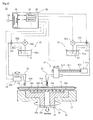
- a silicon single wafer etching apparatus 10 comprises a wafer chuck 12 housed in a chamber, on which a thin disk-like silicon wafer 11 is mounted and retained horizontally.
- the wafer chuck 12 comprises a disk-like base member 13 having a diameter larger than that of the wafer 11 and a holding axis 16 in which an axial part 16a is inserted through a through hole 13a formed in the center of the base member 13 and extended in the vertical direction.
- the holding axis 16 comprises the axial part 16a; a wafer-receiving part 16b having a large diameter, which is integrally formed with the axial part 16a and arranged on the front surface of the axial part 16a; a through hole 16c, which is formed in the center of the holding axis 16 and extends from the bottom face to the top of the holding axis 16 in the vertical direction; a plurality of communicating holes 16d each having an end communicating with the upper end of the through hole 16c and an opposite closed end, where the communicating holes 16d radiate outward around the through hole 16c in the radial direction of the wafer-receiving part 16b; a plurality of ring grooves 16e concentrically formed in the front surface of the wafer-receiving part 16b; and a plurality of small pores 16f allowing the communicating holes 16d and the ring grooves 16e to communicate with each other.
- a vacuum pump (not shown) is connected and communicated with the bottom end of the through hole 16c.
- the front surface of the wafer-receiving part 16b is configured to mount the wafer 11 concentrically with the wafer-receiving part 16b. Then, when the vacuum pump is driven to make the inner pressure of the through hole 16c negative, the negative pressure in the through hole 16c allows the rear surface of the wafer 11 to be adsorbed onto the wafer-receiving part 16b to retain the wafer 11 horizontally.
- the silicon single wafer etching apparatus 10 comprises a spinning device 17 for spinning the wafer 11 around the vertical axis thereof in a horizontal plane.
- the spinning device 17 comprises the holding axis 16, a driving motor (not shown) for rotating the holding axis 16. It is configured that the driving motor rotates the holding axis 16 to allow the wafer 11 retained on the holding axis 16 to be spun with the holding axis 16. Alternatively, it may be configured that when the driving motor rotates the holding axis, the wafer is spun with the holding axis while the base member is being fixed without spinning.
- a plurality of supply nozzles 31, 32 are disposed above and opposite to the front surface of the wafer 11 at different positions in the radial direction of the wafer 11, respectively.
- the plurality of the supply nozzles 31, 32 include a first supply nozzle 31 that supplies a first etching solution 21 to the center of the front surface of the wafer 11 and a second supply nozzle 32 that supplies a second etching solution 22 to the periphery of the front surface of the wafer 11.
- These supply nozzles 31, 32 can be independently moved, respectively by nozzle-moving devices 41, 42 disposed separately.
- the first nozzle-moving device 41 for moving the first supply nozzle 31 comprises: a rotary motor 41a that directly moves the first supply nozzle 31 in the axial direction; a ball screw 41c coaxially connected to a rotary axis 41b of the rotary motor 41a; and a female screw member 41d for holding the first supply nozzle 31 in which a female screw that can be screwed by the ball screw 41c is formed.
- a rotary motor 41a that directly moves the first supply nozzle 31 in the axial direction
- a ball screw 41c coaxially connected to a rotary axis 41b of the rotary motor 41a
- a female screw member 41d for holding the first supply nozzle 31 in which a female screw that can be screwed by the ball screw 41c is formed.
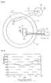
- the first supply nozzle is configured that it can oscillate between a first evacuation position (i.e., a position represented by a two-dot chain line in FIG. 2 ) where a fist discharge opening 31a does not face to the front surface of the wafer 11 and a first liquid supplying position (i.e., a position represented by a solid line) where the first discharge opening 31a faces to the center of the front surface of the wafer 11, due to the first nozzle-moving device 41.
- the second nozzle-moving device 42 that moves the second supply nozzle 32 is mounted on the base end of the second supply nozzle 32 and is provided with a stepping motor 42a that allows the tip of the second supply nozzle 32 to oscillate around the base end.
- the second supply nozzle 32 is configured that it can oscillate between a second evacuation position (i.e., a position represented by a two-dot chain line in FIG. 2 ) where the second discharge opening 32a does not face to the front surface of the wafer 11 and a second liquid supplying position (i.e., a position represented by a solid line) where the second discharge opening 32a faces to the periphery of the front surface of the wafer 11, due to the second nozzle-moving device 42.
- a second evacuation position i.e., a position represented by a two-dot chain line in FIG. 2
- a second liquid supplying position i.e., a position represented by a solid line
- the periphery of the front surface of the wafer 11, where the second discharge opening 32a is positioned on the second liquid supplying position is a given distance within the range of (0.8 to 1.0)D/2 from the center of the wafer 11 to the edge thereof, when the outer diameter of the wafer 11 is D.
- the first supply nozzle 31 is connected to an etching solution supplying device 51 that discharges the first etching solution 21 from the first discharge opening 31a to the center of the front surface of the wafer 11.
- the second supply nozzle 32 is connected to a second etching solution supplying device 52 that discharges the second etching solution 22 from the second discharge opening 32a to the center of the front surface of the wafer 11.
- the first etching solution supplying device 51 comprises a first tank 51a for reserving the first etching solution 21, a first conduit line 51b that allows the first tank 51a to connect to and communicate with the base end of the first supply nozzle 31, a first pump 51c for supplying the first etching solution 21 from the first tank 51a mounted on the first conduit line 51b to the first supply nozzle 31, and a first flow control valve 51d for adjusting the supply flow rate of the first etching solution 21 to the first supply nozzle 31 mounted on the first conduit line 51b.
- the first tank 51a is provided with a first temperature controller (not shown) that is capable of controlling the temperature of the first etching solution 21 in the tank 51a.
- the second etching solution supplying device 52 comprises a second tank 52a for reserving the second etching solution 22, a second conduit line 52b for allowing the second tank 52a to connect to and communicate with the base end of the second supply nozzle 32, a second pump 52c for supplying the second etching solution 22 from the second tank 52a mounted on the second conduit line 52b to the second supply nozzle, and a second flow control valve 52d for adjusting the supply flow rate of the second etching solution 22 to the second supply nozzle 32 mounted on the second conduit line 52b.
- the reference numeral 52e in FIG. 1 is a second return tube for returning a surplus amount of the second etching solution 22 supplied by the second pump 52a to the first tank 51a.
- One or more selected from the groups consisting of temperature, kind, and supply flow rate of each of the first and second etching solutions 21, 22 can be changed.
- the first etching solution 21 is adjusted to a predetermined temperature of preferably in the range of 15 to 40°C, more preferably in the range of 15 to 30°C by the first temperature controller and the second etching solution 22 is adjusted to a predetermined temperature lower than that of the first etching solution 21, preferably in the range of 0 to 30°C, more preferably in the range of 5 to 20°C.
- the reason of why the temperature of the first etching solution 21 is limited in the range of 15 to 40°C is that less than 15°C leads to a decrease in productivity as the etching rate of a main part of the wafer surface lowers and more than 40°C leads to difficulty in maintenance of the degree of wafer flatness as the viscosity of the etching solution decreases.
- the reason of why the temperature of the etching solution 22 is limited in the range of 0 to 30°C is that less than 0°C leads to coagulation of the etching solution and more than 30 °C leads to insufficient effects because of a decrease in difference of the etching rates with the first etching solution.
- the first etching solution 21 used is one preferably having an etching rate of 0.2 to 3 ⁇ m/sec, more preferably 0.3 to 1 ⁇ m/sec at 30°C and the second etching solution 22 used is one having an etching rate smaller than the first etching solution, preferably 0.01 to 1 ⁇ m/sec, more preferably 0.01 to 0.3 ⁇ m/sec.
- the reason of why the etching rate of the first etching solution 21 is limited in the range of 0.2 to 3 ⁇ m /sec is that less than 0.2 ⁇ m/sec leads to a reduction in productivity and more than 3 ⁇ m leads to a difficulty in control of the shape of wafer because of being obstructive to the progress of etching as a matter of practice.
- the reason of why the etching rate of the second etching solution 22 is limited in the range of 0.01 to 1 ⁇ m/sec is that less than 0.01 ⁇ m/sec leads to being virtually incapable of processing etching and controlling wafer forming and more than 1 ⁇ m/sec leads to insufficient effects because of a decrease in difference of the etching rates with the first etching solution.
- the supply flow rate of the first etching solution 21 is adjusted to preferably 1 to 10 l/min, more preferably 2 to 5 l/min.
- the supply flow rate of the second etching solution 22 is adjusted to one smaller than the supply flow rate, and preferably 0.1 to 5 l/min, more preferably 0.5 to 3 l/min.
- the reason of why the supply flow rate of the first etching solution 21 is limited within the range of 1 to 10 l/min is that less than 1 l/min leads to being obstructive to the progress of etching and more than 10 l/min leads to a decrease in effect to plant costs because of enlargement of facilities.
- the reason of why the supply flow rate of the second etching solution 22 is limited within the range of 0.1 to 5 l/min is that less than 0.1 l/min leads to offset of the effects of the second etching solution 22 and more than 5 l/m leads to unstable liquid conditions because of an increase in liquid interference.
- the single wafer etching apparatus 10 has a detecting device 39 for detecting irregularities of the surface of the wafer 11, by a laser reflection scheme utilizing laser reflection at the surface of the wafer 11.
- the detecting device 39 has a detection output connected to a control input of the control device 35, and the control device 35 has a control output connected to the driving motor (not shown) of the spinning device 17, to the first pump 51c and first flow control valve 51d of the etching solution supplying device 51, to the second pump 52c and second flow control valve 52d of the second etching solution supplying device 52, to the rotary motor 41a of the first nozzle-moving device 41, and to the stepping motor 42a of the second nozzle-moving device 42.
- the control device 35 is configured, based on the detection output of the detecting device 39, to control the rotational speed of the driving motor of the spinning device 17, thereby setting the rotational speed of the wafer 11; to control the first pump 51c and first flow control valve 51d of the etching solution supplying device 51 and the second pump 52c and second flow control valve 52d of the second etching solution supplying device 52, thereby determining supplying states of etching solutions from the first and second supply nozzles 31, 32; and to control the rotary motor 41a of the first nozzle-moving device 41 and the stepping motor 42a of the second nozzle-moving device 42, thereby setting the states and positions of the first and second supply nozzles 31, 32, respectively.
- the control device 35 has a calculation device 36 such as a CPU, and a plurality of memories 37, 38, The plurality of memories 37, 38, ... store therein, at least, the surface shape of the wafer 11 before processing, the positions of the first and second supply nozzles 31, 32, the amounts of the etching solutions discharged from the first and second supply nozzles 31, 32, the etched state of the surface of the wafer 11 during the processing, a reference shape of the wafer 11 after the processing, respectively.
- the calculation device 36 is configured to conduct calculations based on the wafer surface shape, nozzle positions, and the like stored in the memories 37, 38, ⁇ , thereby obtaining movements of the nozzles 31, 32 and the discharging states of the etching solutions.
- the memories 37, 38, ⁇ store therein data of the surface shape of the wafer 11 before processing detected by the detecting device 39.
- the memories 37, 38, ⁇ it is possible for the memories 37, 38, ⁇ : to store data of a surface shape of each wafer 11 to be processed, which data is detected by the detecting device 39; to store data of a surface shape of one wafer 11 every predetermined number of wafers 11, which data is representatively detected by the detecting device 39; or to store data of a surface shape of a predetermined wafer 11 every ingot, which data is representatively detected by the detecting device 39; or, it is possible to use a predetermined data for each type of wafer 11.
- the detecting device 39 may be configured as an independent device for measuring a surface shape of a wafer, without placing the detecting device in the single wafer etching apparatus 10.
- a vacuum pump which is connected to and communicated with the bottom end of the through hole 16c of a holding assembly 16 is actuated to make the pressures of the through hole 16c, communicating hole 16d, small hole 16f, and ring groove 16e negative, and the negative pressures then keep the wafer 11 in a horizontal position.
- the driving motor of the spinning device is actuated to allow the wafer 11 to spin in horizontal plane together with the holding assembly 16 and the base member 13.
- only the holding axis 21 may spin, while the base member 19 is not allowed to spin and fixed.
- the rotary motor 41a of the first nozzle-moving device 41 and the stepping motor 42a of the second nozzle-moving device 42 are respectively driven so as to move the first supply nozzle 31 to a position that allows the discharge opening 31a to face to the center of the front surface of the wafer and so as to turn the second supply nozzle 32 to a position that allows the discharge opening 32a to face to the periphery of the front surface of the wafer, and then the first and second pumps 51c, 52c are driven and the first and second flow control valves 51d, 52d are opened so as to supply the first and second etching solutions 21, 22 from the first and second discharge openings 31a, 32a of the first and second supply nozzles 31, 32 to the center of the front surface and the periphery of the front surface of the wafer 11, respectively.
- the first etching solution 21 supplied on the center of the front surface of the wafer 11 gradually moves toward the edge portion of the wafer 11 from the periphery of the front surface of the wafer 11 while etching a processing-strained layer on the front surface of the wafer.
- the centrifugal force with the spinning movement of the wafer 11 makes most of the first and second etching solutions 21, 22 on the wafer 11 into droplets and scatters these droplets outside of the wafer 11, followed by discharging them outside of the chamber.
- the etching rate of the wafer with the first etching solution increases higher than the etching rate of the second etching solution.
- the excessive etching of the periphery of the wafer 11 can be compensated and the wafer 11 can be effectively provided with high flatness.
- the etching rate of the wafer with the first etching solution is higher than the etching rate of the wafer with the second etching solution.
- the etching rate of the wafer with the first etching solution increases higher than the etching rate of the wafer with the second etching solution.
- the excessive etching of the periphery of the wafer 11 is compensated and the wafer can be effectively provided with high flatness.
- the present invention is not limited thereto. Since a surface shape of a wafer after slicing or of a wafer subjected to a mechanical flattening process including lapping after slicing, is not uniform in a radial direction of the wafer and has a thickness variation, undulations, and the like caused thereon, it is enough to conduct etching so as to repair them.
- a wafer obtained by slicing a silicon single crystal ingot was subjected to chamfering and mechanical grinding (lapping), so that there was also prepared a silicon wafer 11 of 300 mm in diameter of which front and back surfaces were flattened.
- a first etching solution 21 was prepared by mixing an aqueous hydrofluoric acid solution at a weight concentration of 50%, an aqueous nitric acid solution at a weight concentration of 70%, and an aqueous phosphoric acid solution at a weight concentration of 85% in a volume ratio of 4 : 7.4 : 6 and then reserved in a first tank 51a heated at 30°C.
- a second etching solution 22 was prepared by mixing 50% by weight concentration of an aqueous fluorine acid solution, 70% by weight concentration of an aqueous nitric acid solution, and 80% by weight concentration of an aqueous phosphoric acid solution in a volume ratio of 4 : 7.4 : 6 and then reserved in a second tank 52a heated at 20°C. Under such conditions, a wafer 11 was mounted on a chuck 12 such that the front surface of the wafer 11 was faced upwardly. Subsequently, the wafer 11 was horizontally rotated.
- the first discharge opening 31a of a first supply nozzle 31 was then reciprocated between - 50 mm to + 50 mm from a basic point (0 mm), which was the center of the front surface of the wafer 11, or the center of the wafer 11, at a velocity of 40 mm/sec, while the second discharge opening 32a of a second supply nozzle 32 was then reciprocated between 30 mm to 0 mm from a basic point (0 mm), which was the periphery of the front surface of the wafer 11, or the periphery of the wafer 11, at a velocity of 40 mm/sec.
- the first etching solution 21 was supplied from the first supply nozzle 31 onto the center of the front surface of the wafer 11 at a flow rate of 4 l/min, while the second etching solution 22 was supplied from the second supply nozzle 32 onto the periphery of the front surface of the wafer 11.
- the first etching solution 21 was spread out from the center of the front surface of the wafer 11 to the edge thereof, while the second etching solution 22 was spread out from the periphery of the front surface of the wafer 11 to the side end thereof, thereby etching a processing-strained layer caused by the planarization processing of the wafer 11. Therefore, the etched wafer was provided for Example 1.
- Etching of wafer was carried out by the same way as that of Example 1, except that a second etching solution used was an etching solution prepared by mixing an aqueous hydrofluoric acid solution at a weight concentration of 50%, an aqueous nitric acid solution at a weight concentration of 70%, and an aqueous phosphoric acid solution at a weight concentration of 85% at a volume ratio of 3 : 8: 6 and then kept at a temperature of 30°C. Therefore, the etched wafer was provided for Example 2.
- a second etching solution used was an etching solution prepared by mixing an aqueous hydrofluoric acid solution at a weight concentration of 50%, an aqueous nitric acid solution at a weight concentration of 70%, and an aqueous phosphoric acid solution at a weight concentration of 85% at a volume ratio of 3 : 8: 6 and then kept at a temperature of 30°C. Therefore, the etched wafer was provided for Example 2.
- Etching of wafer was carried out by the same way as that of Example 1, except that the second etching solution was supplied from the second supply nozzle onto the periphery of the front surface of the wafer at a flow rate of 3 1/min. Therefore, the etched wafer was provided for Example 3.
- Etching of wafer was carried out by the same way as that of Example 1, except that a second etching solution used was an etching solution prepared by mixing an aqueous hydrofluoric acid solution at a weight concentration of 50%, an aqueous nitric acid solution at a weight concentration of 70%, and an aqueous phosphoric acid solution at a weight concentration of 85% at a volume ratio of 3 : 8: 6. Therefore, the etched wafer was provided for Example 4.
- Etching of wafer was carried out by the same way as that of Example 1, except that a second etching solution used was an etching solution prepared by mixing an aqueous hydrofluoric acid solution at a weight concentration of 50%, an aqueous nitric acid solution at a weight concentration of 70%, and an aqueous phosphoric acid solution at a weight concentration of 85% at a volume ratio of 3 : 8: 6 and then kept at a temperature of 30°C. Subsequently, the second etching solution was supplied from the second supply nozzle onto the periphery of the front surface of the wafer at a flow rate of 3 1/min. Therefore, the etched wafer was provided for Example 5.
- a second etching solution used was an etching solution prepared by mixing an aqueous hydrofluoric acid solution at a weight concentration of 50%, an aqueous nitric acid solution at a weight concentration of 70%, and an aqueous phosphoric acid solution at a weight concentration of 85% at a volume
- Etching of wafer was carried out by the same way as that of Example 1, except that the temperature of the second etching solution was kept at 30°C and the second etching solution was supplied from the second supply nozzle to the periphery of the front surface of the wafer at a flow rate of 3 l/min. Therefore, the etched wafer was provided for Example 6.
- Etching of wafer was carried out by the same way as that of Example 1, except that a second etching solution used was an etching solution prepared by mixing an aqueous hydrofluoric acid solution at a weight concentration of 50%, an aqueous nitric acid solution at a weight concentration of 70%, and an aqueous phosphoric acid solution at a weight concentration of 85% at a volume ratio of 3 : 8: 6. Subsequently, the second etching solution was supplied from the second supply nozzle onto the periphery of the front surface of the wafer at a flow rate of 3 1/min. Therefore, the resulting wafer was provided for Example 7.
- a second etching solution used was an etching solution prepared by mixing an aqueous hydrofluoric acid solution at a weight concentration of 50%, an aqueous nitric acid solution at a weight concentration of 70%, and an aqueous phosphoric acid solution at a weight concentration of 85% at a volume ratio of 3 : 8: 6.
- Etching of wafer was carried out by the same way as that of Example 1, except that the second etching solution was kept at a temperature of 30°C.
- the resulting wafer was provided for Comparative Example 1.
- the temperatures (°C) of the first and second solutions, kinds (the percentages of the aqueous fluorinated acid (HF) solution in the mixtures) (% by weight), and flow rates (1/m) of the first and second etching solutions of Examples 1 to 7 and Comparative Example 1 as described above are listed in Table 1 with the differences between the first and second etching solutions.
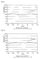
- the measuring results in Example 1 to 7 are shown in FIGS. 3 to 9 and the measuring results in Comparative Example 1 are shown in FIG. 10 .
- Examples 1 to 7 ( FIGS. 3 to 9 ) which represent the surfaces of the respective wafers 11 etched by supplying the first and second etching solutions from the respective first and second supply nozzles, were found to be flat, compared with Comparative Example 1 ( FIG. 10 ) which represents the surface of the wafer etched by supplying the etching solution form the single supply nozzle.
- the present invention can be applied on a method for etching a single wafer such that the front surface of each of wafers is etched one by one while being horizontally retained and rotated.
Landscapes
- Weting (AREA)
Abstract
Description
- The present invention relates to a method for etching the front surface of a wafer one by one, where the wafer is rotated while an etching solution is supplied onto the front surface of the wafer.
- In general, the process for manufacturing a semiconductor wafer comprises the steps of obtaining wafers by cutting and slicing out of a single crystal ingot, and chamfering the respective wafers, mechanical grinding (lapping), etching, mirror-polishing, and cleaning, thereby producing a wafer with highly precise flatness. The wafer, which has been subjected to the steps for mechanical processing, such as block-cutting, rounding, slicing, and lapping, has a damaged layer (i.e., a processing-strained layer) on the surface thereof. In the process for device production, such a processing-strained layer causes crystal defects, such as slip dislocation, and the mechanical strength of the wafer is then decreased. In addition, it has adverse effects on electric characteristics. Therefore, the processing-strained layer should be completely removed. For removing such a processing-strained layer, an etching process is carried out. There are two types of etching: dip-etching and single wafer etching.
- Among the etching processes, the single wafer etching has been regarded as the most suitable etching process, which enables the control of the texture-size and surface roughness of a large-sized wafer. The single wafer etching is a process comprising dropping an etching solution onto the front surface of a flattened single wafer and horizontally rotating (spinning) the wafer to spread out the dripped etching solution over the front surface of the wafer. The etching solution supplied on the wafer is spread out over the surface of the wafer from a supplied point by centrifugal force caused by horizontally spinning the wafer, and finally reaches the edge of the wafer, so that the edge of the wafer as well as the front surface thereof can be also etched at the same time. Furthermore, most of the etching solution supplied is blown off from the edge thereof by centrifugal force and then collected into a cup or the like arranged on an etching device.
- For example, as a process for manufacturing a semiconductor wafer that can effectively remove a processing-strained layer caused by mechanical grinding and retain the flatness of the wafer, there is disclosed one including the following steps; slicing a silicon single crystal ingot; chamfering the end face of the sliced wafer; flattening at least the front surface thereof obtained by slicing the semiconductor ingot by means of surface grinding or lapping; spin-etching the flattened front surface of the wafer; and polishing the etched front surface of the wafer into a mirror surface (e.g., see Patent Document 1).
-
Patent Document 1Japanese Unexamined Patent Application Publication No. 11-135464 Claim 1,FIG. 1 ) - However, in the single wafer etching shown in the
Patent Document 1, the etching solution is quantitatively dripped through a single supply nozzle, so that etching amount may vary. As a result, the front and back surfaces of a silicon wafer, subjected to the etching process, have deficiencies that the flatness of the wafer cannot be maintained after the flattening process including lapping and grinding. In addition, the desired surface roughness of the wafer cannot be obtained. Therefore, for improving the flatness and surface roughness thereof, a large amount of grinding margin is required in the mirror polishing process, so that the subsequent steps in mirror polishing will bear a heavy burden. - Accordingly, the object of the present invention is to provide a method for etching a single wafer, which can effectively attain high flatness and improve the productivity thereof.
- As shown in
FIG. 1 , the invention ofclaim 1 is an improvement of a method for etching a single wafer, wherein a single thin disk-like silicon wafer 11 sliced from a silicon single crystal ingot is spun to etch a front surface of thewafer 11 withetching solutions - The characteristic feature thereof lies in that a plurality of etching
solution supply nozzles wafer 11 at different portions in the radial direction of the wafer, respectively and one or more conditions selected from the group consisting of temperatures, kinds, and supply flow rates ofetching solutions supply nozzles - In the single wafer etching apparatus as described in
claim 1, plural etchingsolution supply nozzles wafer 11 at different portions in the radial direction of the wafer, respectively. From these etchingsolution supply nozzles optimum etching solutions wafer 11, are supplied to the respective portions described above. Therefore, the degree of freedom to control the distribution of etching amount on the surface of thewafer 11 in the wafer surface can be increased and thewafer 11 can be thus effectively provided with high flatness. - The invention of
claim 2 is related to the invention ofclaim 1, as further shown inFig. 1 , wherein the plurality of etchingsolution supply nozzles first supply nozzle 31 that supplies afirst etching solution 21 to the center of the front surface of thewafer 11 and asecond supply nozzle 32 that supplies asecond etching solution 22 to the periphery of the front surface of thewafer 11, wherein the temperature of thefirst etching solution 21 supplied from thefirst supply nozzle 31 to the center of the front surface of thewafer 11 is higher than the temperature of thesecond etching solution 22 supplied from thesecond supply nozzle 32 to the periphery of the front surface of thewafer 11. - In the method for etching a single wafer as described in
claim 2, the temperature of the first etching solution supplied on the center of the front surface of the wafer is higher than the temperature of the second etching solution supplied to the periphery of the front surface of the wafer, so that the rate of etching the wafer with the first etching solution can be higher than the rate of etching the wafer with the second solution. Typically, in the method for etching a single wafer, due to both the generation of heat by reaction and the transfer of a liquid in the peripheral direction of the wafer by centrifugal force, excessive etching may tend to occur in the periphery. However, in the method for etching a single wafer of the present invention, the temperature of thefirst etching solution 21 supplied from thefirst supply nozzle 31 to the center of the front surface of thewafer 11 is higher than the temperature of thesecond etching solution 22 supplied from thesecond supply nozzle 32 to the periphery of the front surface of thewafer 11, so that the periphery of thewafer 11 can be prevented from excessive etching. Therefore, thewafer 11 can be effectively provided with high flatness. - The invention of
claim 3 is related to the invention ofclaim 1, as shown inFIG. 1 , wherein the plurality of etchingsolution supply nozzles first supply nozzle 31 that supplies afirst etching solution 21 to the center of the front surface of thewafer 11 and asecond supply nozzle 32 that supplies asecond etching solution 22 to the periphery of the front surface of thewafer 11, where thefirst etching solution 21 supplied from thefirst supply nozzle 31 to the center of the front surface of thewafer 11 is an etching solution having a higher etching rate than that of thesecond etching solution 22 supplied from thesecond supply nozzle 32 to the periphery of the front surface of thewafer 11. - In the method for etching a single wafer as described in
claim 3, thefirst etching solution 21 supplied from thefirst supply nozzle 31 to the center of the front surface of thewafer 11 is an etching solution having a higher etching rate than that of thesecond etching solution 22 supplied from thesecond supply nozzle 32 to the periphery of the front surface of thewafer 11, so that the etching rate of the wafer with the first etching solution can be higher than the etching rate of the wafer with second etching solution. Typically, in the method for etching a single wafer, due to both the generation of heat by reaction and the transfer of a liquid in the peripheral direction of the wafer by centrifugal force, excessive etching may tend to occur in the periphery. However, in the method for etching a single wafer of the present invention, thefirst etching solution 21 supplied from thefirst supply nozzle 31 to the center of the front surface of thewafer 11 uses the kind of an etching solution having an etching rate higher than that of thesecond etching solution 22 supplied from thesecond supply nozzle 32 to the periphery of the front surface of thewafer 11, so that the periphery of thewafer 11 can be prevented from excessive etching. Therefore, thewafer 11 can be effectively provided with high flatness. - The invention of
claim 4 is related to the invention ofclaim 1, as further shown inFIG. 1 , wherein the plurality of etchingsolution supply nozzles first supply nozzle 31 that supplies afirst etching solution 21 to the center of the front surface of thewafer 11 and asecond supply nozzle 32 that supplies asecond etching solution 22 to the periphery of the front surface of thewafer 11, where the supply flow rate of thefirst etching solution 21 supplied from thefirst supply nozzle 31 to the center of the front surface of thewafer 11 is higher than the supply flow rate of thesecond etching solution 22 supplied from thesecond supply nozzle 32 to the periphery of the front surface of thewafer 11. - In the method for etching a single wafer as described in
claim 4, the supply flow rate of thefirst etching solution 21 supplied from thefirst supply nozzle 31 to the center of the front surface of thewafer 11 is higher than the supply flow rate of thesecond etching solution 22 supplied from thesecond supply nozzle 32 to the periphery of the front surface of thewafer 11, so that the etching rate of the wafer with the first etching solution can be higher than the etching rate of the wafer with the second etching solution. Typically, in the method for etching a single wafer, due to both the generation of heat by reaction and the transfer of a liquid in the peripheral direction of the wafer by centrifugal force, excessive etching may tend to occur in the periphery. However, in the method for etching a single wafer of the present invention, the supply flow rate of thefirst etching solution 21 supplied from thefirst supply nozzle 31 to the center of the front surface of thewafer 11 is higher than the supply flow rate of thesecond etching solution 22 supplied from thesecond supply nozzle 32 to the periphery of the front surface of thewafer 11, so that the periphery of thewafer 11 can be prevented from excessive etching. Therefore, thewafer 11 can be effectively provided with high flatness. - As described above, according to the present invention, a plurality of etching solution supply nozzles are disposed above and opposite to the front surface of the wafer at different portions in the radial direction of the wafer, respectively and one or more conditions selected from the group consisting of temperatures, kinds, and supply flow rates of etching solutions from the plurality of etching solution supply nozzles are then changed. Therefore, an optimum etching solution, where the temperature, kind, or supply flow rate thereof are adjusted, is supplied to each part of the wafer from the plurality of etching solution supply nozzles. As a result, the degree of freedom to control the distribution of etching amount on the surface of the wafer can be increased and the wafer can be effectively provided with high flatness, thereby allowing the wafer to be easily subjected to the subsequent step of grinding.
- In addition, the temperature of the first etching solution supplied from the first supply nozzle to the center of the front surface of the wafer is higher than the temperature of the second etching solution supplied from the second supply nozzle to the periphery of the front surface of the wafer, so that the etching rate of the wafer with the first etching solution can be higher than the etching rate of the wafer with the second etching solution. As a result, the excessive etching of the periphery of the wafer can be repaired, thereby efficiently providing the wafer with high flatness.
- In addition, an etching solution used as the first etching solution supplied from the first supply nozzle to the center of the front surface of the wafer has a higher etching rate than that of the second etching solution supplied from the second supply nozzle to the periphery of the front surface of the wafer, so that the etching rate of the wafer with the first etching solution can be higher than the etching rate of the wafer with the second etching solution. As a result, the excessive etching of the periphery of the wafer can be repaired, thereby efficiently providing the wafer with high flatness.
- Furthermore, the supply flow rate of the first etching solution supplied from the first supply nozzle to the center of the front surface of the wafer is higher than that of the second etching solution supplied from the second supply nozzle to the periphery of the front surface of the wafer, so that the etching rate of the wafer with the first etching solution can be higher than the etching rate of the wafer with the second etching solution. As a result, the excessive etching of the periphery of the wafer can be repaired, thereby efficiently providing the wafer with high flatness.
-
-
FIG. 1 is a vertical cross-sectional view of the substantial part of a method for etching a single wafer according to an embodiment of the present invention; -
FIG. 2 is a plane view showing the relationship between first and second supply nozzles and the wafer; -
FIG. 3 is a graph showing variation in the wafer thickness in Example 1; -
FIG. 4 is a graph showing variation in the wafer thickness in Example 2; -
FIG. 5 is a graph showing variation in the wafer thickness in Example 3; -
FIG. 6 is a graph showing variation in the wafer thickness in Example 4; -
FIG. 7 is a graph showing variation in the wafer thickness in Example 5; -
FIG. 8 is a graph showing variation in the wafer thickness in Example 6; -
FIG. 9 is a graph showing variation in the wafer thickness in Example 7; and -
FIG. 10 is a graph showing variation in the wafer thickness in Comparative Example 1. - Hereinafter, preferred embodiments for carrying out the present invention will be described in more details with reference to the attached drawings.
- As shown in
FIG. 1 , a silicon singlewafer etching apparatus 10 comprises awafer chuck 12 housed in a chamber, on which a thin disk-like silicon wafer 11 is mounted and retained horizontally. Thewafer chuck 12 comprises a disk-like base member 13 having a diameter larger than that of thewafer 11 and a holdingaxis 16 in which anaxial part 16a is inserted through a through hole 13a formed in the center of thebase member 13 and extended in the vertical direction. The holdingaxis 16 comprises theaxial part 16a; a wafer-receivingpart 16b having a large diameter, which is integrally formed with theaxial part 16a and arranged on the front surface of theaxial part 16a; a throughhole 16c, which is formed in the center of the holdingaxis 16 and extends from the bottom face to the top of the holdingaxis 16 in the vertical direction; a plurality of communicatingholes 16d each having an end communicating with the upper end of the throughhole 16c and an opposite closed end, where the communicatingholes 16d radiate outward around the throughhole 16c in the radial direction of the wafer-receivingpart 16b; a plurality ofring grooves 16e concentrically formed in the front surface of the wafer-receivingpart 16b; and a plurality ofsmall pores 16f allowing the communicatingholes 16d and thering grooves 16e to communicate with each other. A vacuum pump (not shown) is connected and communicated with the bottom end of the throughhole 16c. The front surface of the wafer-receivingpart 16b is configured to mount thewafer 11 concentrically with the wafer-receivingpart 16b. Then, when the vacuum pump is driven to make the inner pressure of the throughhole 16c negative, the negative pressure in the throughhole 16c allows the rear surface of thewafer 11 to be adsorbed onto the wafer-receivingpart 16b to retain thewafer 11 horizontally. In addition, the silicon singlewafer etching apparatus 10 comprises aspinning device 17 for spinning thewafer 11 around the vertical axis thereof in a horizontal plane. Thespinning device 17 comprises the holdingaxis 16, a driving motor (not shown) for rotating the holdingaxis 16. It is configured that the driving motor rotates the holdingaxis 16 to allow thewafer 11 retained on the holdingaxis 16 to be spun with the holdingaxis 16. Alternatively, it may be configured that when the driving motor rotates the holding axis, the wafer is spun with the holding axis while the base member is being fixed without spinning. - In addition, as shown in
FIG. 1 andFIG. 2 , a plurality ofsupply nozzles wafer 11 at different positions in the radial direction of thewafer 11, respectively. In this embodiment, the plurality of thesupply nozzles first supply nozzle 31 that supplies afirst etching solution 21 to the center of the front surface of thewafer 11 and asecond supply nozzle 32 that supplies asecond etching solution 22 to the periphery of the front surface of thewafer 11. Thesesupply nozzles devices device 41 for moving thefirst supply nozzle 31 comprises: arotary motor 41a that directly moves thefirst supply nozzle 31 in the axial direction; aball screw 41c coaxially connected to arotary axis 41b of therotary motor 41a; and afemale screw member 41d for holding thefirst supply nozzle 31 in which a female screw that can be screwed by theball screw 41c is formed. By allowing theball screw 41c to rotate by rotating therotational axis 41b of therotary motor 41a, thefirst supply nozzle 31 can be directly moved in the axial direction thereof together with thefemale screw member 41d. In addition, as illustrated inFIG. 2 in detail, the first supply nozzle is configured that it can oscillate between a first evacuation position (i.e., a position represented by a two-dot chain line inFIG. 2 ) where afist discharge opening 31a does not face to the front surface of thewafer 11 and a first liquid supplying position (i.e., a position represented by a solid line) where the first discharge opening 31a faces to the center of the front surface of thewafer 11, due to the first nozzle-movingdevice 41. On the other hand, the second nozzle-movingdevice 42 that moves thesecond supply nozzle 32 is mounted on the base end of thesecond supply nozzle 32 and is provided with a steppingmotor 42a that allows the tip of thesecond supply nozzle 32 to oscillate around the base end. Furthermore, thesecond supply nozzle 32 is configured that it can oscillate between a second evacuation position (i.e., a position represented by a two-dot chain line inFIG. 2 ) where the second discharge opening 32a does not face to the front surface of thewafer 11 and a second liquid supplying position (i.e., a position represented by a solid line) where the second discharge opening 32a faces to the periphery of the front surface of thewafer 11, due to the second nozzle-movingdevice 42. Here, the periphery of the front surface of thewafer 11, where the second discharge opening 32a is positioned on the second liquid supplying position, is a given distance within the range of (0.8 to 1.0)D/2 from the center of thewafer 11 to the edge thereof, when the outer diameter of thewafer 11 is D. - Referring again to
FIG. 1 , thefirst supply nozzle 31 is connected to an etchingsolution supplying device 51 that discharges thefirst etching solution 21 from the first discharge opening 31a to the center of the front surface of thewafer 11. In contrast, thesecond supply nozzle 32 is connected to a second etchingsolution supplying device 52 that discharges thesecond etching solution 22 from the second discharge opening 32a to the center of the front surface of thewafer 11. The first etchingsolution supplying device 51 comprises afirst tank 51a for reserving thefirst etching solution 21, afirst conduit line 51b that allows thefirst tank 51a to connect to and communicate with the base end of thefirst supply nozzle 31, afirst pump 51c for supplying thefirst etching solution 21 from thefirst tank 51a mounted on thefirst conduit line 51b to thefirst supply nozzle 31, and a firstflow control valve 51d for adjusting the supply flow rate of thefirst etching solution 21 to thefirst supply nozzle 31 mounted on thefirst conduit line 51b. Thefirst tank 51a is provided with a first temperature controller (not shown) that is capable of controlling the temperature of thefirst etching solution 21 in thetank 51a. Here, thereference numeral 51e inFIG. 1 is a first return tube for returning a surplus amount of thefirst etching solution 21 supplied by thefirst pump 51a to thefirst tank 51a. In contrast, the second etchingsolution supplying device 52 comprises asecond tank 52a for reserving thesecond etching solution 22, asecond conduit line 52b for allowing thesecond tank 52a to connect to and communicate with the base end of thesecond supply nozzle 32, asecond pump 52c for supplying thesecond etching solution 22 from thesecond tank 52a mounted on thesecond conduit line 52b to the second supply nozzle, and a secondflow control valve 52d for adjusting the supply flow rate of thesecond etching solution 22 to thesecond supply nozzle 32 mounted on thesecond conduit line 52b. Here, thereference numeral 52e inFIG. 1 is a second return tube for returning a surplus amount of thesecond etching solution 22 supplied by thesecond pump 52a to thefirst tank 51a. - One or more selected from the groups consisting of temperature, kind, and supply flow rate of each of the first and
second etching solutions second etching solution first etching solution 21 is adjusted to a predetermined temperature of preferably in the range of 15 to 40°C, more preferably in the range of 15 to 30°C by the first temperature controller and thesecond etching solution 22 is adjusted to a predetermined temperature lower than that of thefirst etching solution 21, preferably in the range of 0 to 30°C, more preferably in the range of 5 to 20°C. Here, the reason of why the temperature of thefirst etching solution 21 is limited in the range of 15 to 40°C is that less than 15°C leads to a decrease in productivity as the etching rate of a main part of the wafer surface lowers and more than 40°C leads to difficulty in maintenance of the degree of wafer flatness as the viscosity of the etching solution decreases. The reason of why the temperature of theetching solution 22 is limited in the range of 0 to 30°C is that less than 0°C leads to coagulation of the etching solution and more than 30 °C leads to insufficient effects because of a decrease in difference of the etching rates with the first etching solution. - Furthermore, when each of the kinds of the first and
second etching solution first etching solution 21 used is one preferably having an etching rate of 0.2 to 3 µm/sec, more preferably 0.3 to 1 µm/sec at 30°C and thesecond etching solution 22 used is one having an etching rate smaller than the first etching solution, preferably 0.01 to 1 µm/sec, more preferably 0.01 to 0.3 µm/sec. Here, the reason of why the etching rate of thefirst etching solution 21 is limited in the range of 0.2 to 3 µm /sec is that less than 0.2 µm/sec leads to a reduction in productivity and more than 3 µm leads to a difficulty in control of the shape of wafer because of being obstructive to the progress of etching as a matter of practice. The reason of why the etching rate of thesecond etching solution 22 is limited in the range of 0.01 to 1 µm/sec is that less than 0.01 µm/sec leads to being virtually incapable of processing etching and controlling wafer forming and more than 1 µm/sec leads to insufficient effects because of a decrease in difference of the etching rates with the first etching solution. The abovefirst etching solution 21 may be one having a weight ratio (% by weight) of fluorinated acid (HF) : nitric acid (HNO3) : phosphate (H3PO4) : water (H2O) = (5 to 20) : (5 to 40) : (30 to 40) : remainder (rest) after mixing with an aqueous acid solution. Thesecond etching solution 22 may be one having a weight ratio (% by weight) of fluorinated acid (HF) : nitric acid (HNO3) : phosphate (H3PO4) : water (H2O) = (0.5 to 10) : (20 to 50) : (30 to 40) : remainder (rest). - Furthermore, when the supply flow rate of each of the first and
second etching solutions first etching solution 21 is adjusted to preferably 1 to 10 l/min, more preferably 2 to 5 l/min. The supply flow rate of thesecond etching solution 22 is adjusted to one smaller than the supply flow rate, and preferably 0.1 to 5 l/min, more preferably 0.5 to 3 l/min. Here, the reason of why the supply flow rate of thefirst etching solution 21 is limited within the range of 1 to 10 l/min is that less than 1 l/min leads to being obstructive to the progress of etching and more than 10 l/min leads to a decrease in effect to plant costs because of enlargement of facilities. The reason of why the supply flow rate of thesecond etching solution 22 is limited within the range of 0.1 to 5 l/min is that less than 0.1 l/min leads to offset of the effects of thesecond etching solution 22 and more than 5 l/m leads to unstable liquid conditions because of an increase in liquid interference. - Further, the single
wafer etching apparatus 10 has a detectingdevice 39 for detecting irregularities of the surface of thewafer 11, by a laser reflection scheme utilizing laser reflection at the surface of thewafer 11. The detectingdevice 39 has a detection output connected to a control input of thecontrol device 35, and thecontrol device 35 has a control output connected to the driving motor (not shown) of thespinning device 17, to thefirst pump 51c and firstflow control valve 51d of the etchingsolution supplying device 51, to thesecond pump 52c and secondflow control valve 52d of the second etchingsolution supplying device 52, to therotary motor 41a of the first nozzle-movingdevice 41, and to the steppingmotor 42a of the second nozzle-movingdevice 42. Thecontrol device 35 is configured, based on the detection output of the detectingdevice 39, to control the rotational speed of the driving motor of thespinning device 17, thereby setting the rotational speed of thewafer 11; to control thefirst pump 51c and firstflow control valve 51d of the etchingsolution supplying device 51 and thesecond pump 52c and secondflow control valve 52d of the second etchingsolution supplying device 52, thereby determining supplying states of etching solutions from the first andsecond supply nozzles rotary motor 41a of the first nozzle-movingdevice 41 and the steppingmotor 42a of the second nozzle-movingdevice 42, thereby setting the states and positions of the first andsecond supply nozzles control device 35 has acalculation device 36 such as a CPU, and a plurality ofmemories memories wafer 11 before processing, the positions of the first andsecond supply nozzles second supply nozzles wafer 11 during the processing, a reference shape of thewafer 11 after the processing, respectively. Thecalculation device 36 is configured to conduct calculations based on the wafer surface shape, nozzle positions, and the like stored in thememories nozzles memories wafer 11 before processing detected by the detectingdevice 39. Note that it is possible for thememories wafer 11 to be processed, which data is detected by the detectingdevice 39; to store data of a surface shape of onewafer 11 every predetermined number ofwafers 11, which data is representatively detected by the detectingdevice 39; or to store data of a surface shape of apredetermined wafer 11 every ingot, which data is representatively detected by the detectingdevice 39; or, it is possible to use a predetermined data for each type ofwafer 11. Moreover, the detectingdevice 39 may be configured as an independent device for measuring a surface shape of a wafer, without placing the detecting device in the singlewafer etching apparatus 10. - The method for etching the
wafer 11 using the singlewafer etching apparatus 10 as constructed above will be described. - At first, in the state that the
wafer 11 is mounted on thechuck 12, a vacuum pump, which is connected to and communicated with the bottom end of the throughhole 16c of a holdingassembly 16, is actuated to make the pressures of the throughhole 16c, communicatinghole 16d,small hole 16f, andring groove 16e negative, and the negative pressures then keep thewafer 11 in a horizontal position. In this state, the driving motor of the spinning device is actuated to allow thewafer 11 to spin in horizontal plane together with the holdingassembly 16 and thebase member 13. Alternatively, only the holdingaxis 21 may spin, while the base member 19 is not allowed to spin and fixed. Subsequently, therotary motor 41a of the first nozzle-movingdevice 41 and the steppingmotor 42a of the second nozzle-movingdevice 42 are respectively driven so as to move thefirst supply nozzle 31 to a position that allows thedischarge opening 31a to face to the center of the front surface of the wafer and so as to turn thesecond supply nozzle 32 to a position that allows thedischarge opening 32a to face to the periphery of the front surface of the wafer, and then the first andsecond pumps flow control valves second etching solutions second discharge openings second supply nozzles wafer 11, respectively. Thefirst etching solution 21 supplied on the center of the front surface of thewafer 11 gradually moves toward the edge portion of thewafer 11 from the periphery of the front surface of thewafer 11 while etching a processing-strained layer on the front surface of the wafer. The centrifugal force with the spinning movement of thewafer 11 makes most of the first andsecond etching solutions wafer 11 into droplets and scatters these droplets outside of thewafer 11, followed by discharging them outside of the chamber. - Here, when the first etching solution supplied from the first supply nozzle to the center of the front surface of the wafer is set to a temperature higher than the temperature of the second etching solution supplied from the second supply nozzle to the periphery of the front surface of the wafer, the etching rate of the wafer with the first etching solution increases higher than the etching rate of the second etching solution. As a result, the excessive etching of the periphery of the
wafer 11 can be compensated and thewafer 11 can be effectively provided with high flatness. In addition, when the first etching solution supplied from the first supply nozzle to the center of the front surface of the wafer is an etching solution having a higher etching rate than that of the second etching solution supplied from the second supply nozzle to the periphery of the front surface of the wafer, the etching rate of the wafer with the first etching solution is higher than the etching rate of the wafer with the second etching solution. As a result, the excessive etching of the periphery of thewafer 11 can be compensated and the wafer can be effectively provided with high flatness. Furthermore, when the supply flow rate of the first etching solution supplied from the first supply nozzle to the center of the front surface of the wafer is higher than the supply flow rate of the second etching solution supplied from the second supply nozzle to the periphery of the front surface of the wafer, the etching rate of the wafer with the first etching solution increases higher than the etching rate of the wafer with the second etching solution. As a result, the excessive etching of the periphery of thewafer 11 is compensated and the wafer can be effectively provided with high flatness. - Note that although the embodiment has been explained for a situation for repairing an excessive etching of a periphery of a
wafer 11 which becomes problematic upon etching by a single supply nozzle, the present invention is not limited thereto. Since a surface shape of a wafer after slicing or of a wafer subjected to a mechanical flattening process including lapping after slicing, is not uniform in a radial direction of the wafer and has a thickness variation, undulations, and the like caused thereon, it is enough to conduct etching so as to repair them. Namely, it is possible to effectively attain high flatness of awafer 11, by previously measuring a surface shape of thewafer 11 before etching, and by adjusting one or more conditions selected from the group consisting of temperatures, kinds, and supply flow rates of etching solutions to be supplied from the etching solution supply nozzles, depending on the surface shape of the wafer, so as to compensate for a difference between the measured surface shape and an intended surface shape of thewafer 11 after etching. Furthermore, although the above embodiment has been described for a situation where the number of supply nozzles is two, the supply nozzles may be three, four, or more, in number. - Next, Examples of the present invention will be described in more detail with reference to Comparative Example.
- As shown in
FIGS. 1 and2 , a wafer obtained by slicing a silicon single crystal ingot was subjected to chamfering and mechanical grinding (lapping), so that there was also prepared asilicon wafer 11 of 300 mm in diameter of which front and back surfaces were flattened. In addition, afirst etching solution 21 was prepared by mixing an aqueous hydrofluoric acid solution at a weight concentration of 50%, an aqueous nitric acid solution at a weight concentration of 70%, and an aqueous phosphoric acid solution at a weight concentration of 85% in a volume ratio of 4 : 7.4 : 6 and then reserved in afirst tank 51a heated at 30°C. On the other hand, asecond etching solution 22 was prepared by mixing 50% by weight concentration of an aqueous fluorine acid solution, 70% by weight concentration of an aqueous nitric acid solution, and 80% by weight concentration of an aqueous phosphoric acid solution in a volume ratio of 4 : 7.4 : 6 and then reserved in asecond tank 52a heated at 20°C. Under such conditions, awafer 11 was mounted on achuck 12 such that the front surface of thewafer 11 was faced upwardly. Subsequently, thewafer 11 was horizontally rotated. After that, the first discharge opening 31a of afirst supply nozzle 31 was then reciprocated between - 50 mm to + 50 mm from a basic point (0 mm), which was the center of the front surface of thewafer 11, or the center of thewafer 11, at a velocity of 40 mm/sec, while the second discharge opening 32a of asecond supply nozzle 32 was then reciprocated between 30 mm to 0 mm from a basic point (0 mm), which was the periphery of the front surface of thewafer 11, or the periphery of thewafer 11, at a velocity of 40 mm/sec. Under such conditions, thefirst etching solution 21 was supplied from thefirst supply nozzle 31 onto the center of the front surface of thewafer 11 at a flow rate of 4 l/min, while thesecond etching solution 22 was supplied from thesecond supply nozzle 32 onto the periphery of the front surface of thewafer 11. By centrifugal force generated by the horizontal spinning of thewafer 11, thefirst etching solution 21 was spread out from the center of the front surface of thewafer 11 to the edge thereof, while thesecond etching solution 22 was spread out from the periphery of the front surface of thewafer 11 to the side end thereof, thereby etching a processing-strained layer caused by the planarization processing of thewafer 11. Therefore, the etched wafer was provided for Example 1. - Etching of wafer was carried out by the same way as that of Example 1, except that a second etching solution used was an etching solution prepared by mixing an aqueous hydrofluoric acid solution at a weight concentration of 50%, an aqueous nitric acid solution at a weight concentration of 70%, and an aqueous phosphoric acid solution at a weight concentration of 85% at a volume ratio of 3 : 8: 6 and then kept at a temperature of 30°C. Therefore, the etched wafer was provided for Example 2.
- Etching of wafer was carried out by the same way as that of Example 1, except that the second etching solution was supplied from the second supply nozzle onto the periphery of the front surface of the wafer at a flow rate of 3 1/min. Therefore, the etched wafer was provided for Example 3.
- Etching of wafer was carried out by the same way as that of Example 1, except that a second etching solution used was an etching solution prepared by mixing an aqueous hydrofluoric acid solution at a weight concentration of 50%, an aqueous nitric acid solution at a weight concentration of 70%, and an aqueous phosphoric acid solution at a weight concentration of 85% at a volume ratio of 3 : 8: 6. Therefore, the etched wafer was provided for Example 4.
- Etching of wafer was carried out by the same way as that of Example 1, except that a second etching solution used was an etching solution prepared by mixing an aqueous hydrofluoric acid solution at a weight concentration of 50%, an aqueous nitric acid solution at a weight concentration of 70%, and an aqueous phosphoric acid solution at a weight concentration of 85% at a volume ratio of 3 : 8: 6 and then kept at a temperature of 30°C. Subsequently, the second etching solution was supplied from the second supply nozzle onto the periphery of the front surface of the wafer at a flow rate of 3 1/min. Therefore, the etched wafer was provided for Example 5.
- Etching of wafer was carried out by the same way as that of Example 1, except that the temperature of the second etching solution was kept at 30°C and the second etching solution was supplied from the second supply nozzle to the periphery of the front surface of the wafer at a flow rate of 3 l/min. Therefore, the etched wafer was provided for Example 6.
- Etching of wafer was carried out by the same way as that of Example 1, except that a second etching solution used was an etching solution prepared by mixing an aqueous hydrofluoric acid solution at a weight concentration of 50%, an aqueous nitric acid solution at a weight concentration of 70%, and an aqueous phosphoric acid solution at a weight concentration of 85% at a volume ratio of 3 : 8: 6. Subsequently, the second etching solution was supplied from the second supply nozzle onto the periphery of the front surface of the wafer at a flow rate of 3 1/min. Therefore, the resulting wafer was provided for Example 7.
- Etching of wafer was carried out by the same way as that of Example 1, except that the second etching solution was kept at a temperature of 30°C. The resulting wafer was provided for Comparative Example 1.
- The temperatures (°C) of the first and second solutions, kinds (the percentages of the aqueous fluorinated acid (HF) solution in the mixtures) (% by weight), and flow rates (1/m) of the first and second etching solutions of Examples 1 to 7 and Comparative Example 1 as described above are listed in Table 1 with the differences between the first and second etching solutions.
-
[Table 1] 1st Etching Solution 2nd Etching Solution Differences between 1st and 2nd Etching solution Temp. (°C) HF conc. (wt%) Supply flow rate (l/min) Temp. (°C) HF conc. (wt%) Supply flow rate (l/min) Example 1 30 9 4 20 9 4 Temperatures Example 2 30 9 4 30 7 4 Concentrations Example 3 30 9 4 30 9 3 Flow rates Example 4 30 9 4 20 7 4 Temperatures, Concentrations Example 5 30 9 4 30 7 3 Concentrations, Flow rates Example 6 30 9 4 20 9 3 Temperatures, Flow rates Example 7 30 9 4 20 7 3 Temperatures, Concentrations, Flow rates Comparat ive Example 1 30 9 4 30 9 4 Nothing - Thicknesses of the respective silicon wafers, on which the single wafer etching procedures were performed according to Examples 1 to 7 and Comparative Example 1, were measured using a flatness-measuring equipment (Wafercom, manufactured by Doi Precision Lapping Co., Ltd.), respectively. The measuring results in Example 1 to 7 are shown in
FIGS. 3 to 9 and the measuring results in Comparative Example 1 are shown inFIG. 10 . As is evident fromFIGS. 3 to 10 , Examples 1 to 7 (FIGS. 3 to 9 ), which represent the surfaces of therespective wafers 11 etched by supplying the first and second etching solutions from the respective first and second supply nozzles, were found to be flat, compared with Comparative Example 1 (FIG. 10 ) which represents the surface of the wafer etched by supplying the etching solution form the single supply nozzle. - Therefore, the present invention can be applied on a method for etching a single wafer such that the front surface of each of wafers is etched one by one while being horizontally retained and rotated.
Claims (4)
- A method for etching a single wafer, wherein a single thin disk-like silicon wafer sliced from a silicon single crystal ingot is spun to etch a front surface of the wafer with etching solutions supplied thereto, comprising the steps of:disposing a plurality of etching solution supply nozzles above and opposite to the front surface of the wafer at different portions in the radial direction of the wafer; andchanging one or more conditions selected from the group consisting of temperatures, kinds, and supply flow rates of etching solutions from the plurality of etching solution supply nozzles.
- The method for etching a single wafer according to claim 1, wherein
the plurality of etching solution supply nozzles include a first supply nozzle that supplies a first etching solution to the center of the front surface of the wafer and a second supply nozzle that supplies a second etching solution to the periphery of the front surface of the wafer, where
the temperature of the first etching solution supplied from the first supply nozzle to the center of the front surface of the wafer is higher than the temperature of the second etching solution supplied from the second supply nozzle to the periphery of the front surface of the wafer. - The method for etching a single wafer according to claim 1, wherein
the plurality of etching solution supply nozzles include a first supply nozzle that supplies a first etching solution to the center of the front surface of the wafer and a second supply nozzle that supplies a second etching solution to the periphery of the front surface of the wafer, where
the first etching solution supplied from the first supply nozzle to the center of the front surface of the wafer is an etching solution having a higher etching rate than that of the second etching solution supplied from the second supply nozzle to the periphery of the front surface of the wafer. - The method for etching a single wafer according to claim 1, wherein
the plurality of etching solution supply nozzles include a first supply nozzle that supplies a first etching solution to the center of the front surface of the wafer and a second supply nozzle that supplies a second etching solution to the periphery of the front surface of the wafer, where
the supply flow rate of the first etching solution supplied from the first supply nozzle to the center of the front surface of the wafer is higher than the supply flow rate of the second etching solution supplied from the second supply nozzle to the periphery of the front surface of the wafer.
Applications Claiming Priority (2)
| Application Number | Priority Date | Filing Date | Title |
|---|---|---|---|
| JP2006021900 | 2006-01-31 | ||
| PCT/JP2007/051034 WO2007088755A1 (en) | 2006-01-31 | 2007-01-24 | Single wafer etching method |
Publications (2)
| Publication Number | Publication Date |
|---|---|
| EP1981072A1 true EP1981072A1 (en) | 2008-10-15 |
| EP1981072A4 EP1981072A4 (en) | 2009-01-21 |
Family
ID=38327334
Family Applications (1)
| Application Number | Title | Priority Date | Filing Date |
|---|---|---|---|
| EP07707285A Ceased EP1981072A4 (en) | 2006-01-31 | 2007-01-24 | METHOD FOR ETCHING SINGLE PLATE |
Country Status (8)
| Country | Link |
|---|---|
| US (1) | US8466071B2 (en) |
| EP (1) | EP1981072A4 (en) |
| JP (1) | JP4974904B2 (en) |
| KR (1) | KR20080082010A (en) |
| CN (1) | CN101379599B (en) |
| MY (1) | MY148726A (en) |
| TW (1) | TWI339861B (en) |
| WO (1) | WO2007088755A1 (en) |
Families Citing this family (33)
| Publication number | Priority date | Publication date | Assignee | Title |
|---|---|---|---|---|
| US7368285B2 (en) | 2001-03-07 | 2008-05-06 | Senomyx, Inc. | Heteromeric umami T1R1/T1R3 taste receptors and isolated cells that express same |
| US7955982B2 (en) * | 2006-01-20 | 2011-06-07 | Sumco Corporation | Method for smoothing wafer surface and apparatus used therefor |
| JP2008218545A (en) * | 2007-03-01 | 2008-09-18 | Sumco Corp | Wafer single wafer etching system |
| JP2010003847A (en) * | 2008-06-19 | 2010-01-07 | Sumco Corp | Manufacturing method of semiconductor wafer |
| JP5026356B2 (en) * | 2008-06-26 | 2012-09-12 | Sumco Techxiv株式会社 | Diffusion wafer manufacturing method |
| JP2012186187A (en) * | 2009-07-08 | 2012-09-27 | Sharp Corp | Etching method and etching process device |
| KR101308352B1 (en) | 2011-12-16 | 2013-09-17 | 주식회사 엘지실트론 | Apparatus for single wafer etching |
| JP6064875B2 (en) * | 2013-11-25 | 2017-01-25 | 東京エレクトロン株式会社 | Liquid processing apparatus, liquid processing method, and storage medium |
| JP6027523B2 (en) * | 2013-12-05 | 2016-11-16 | 東京エレクトロン株式会社 | Substrate processing apparatus, substrate processing method, and recording medium recording substrate processing program |
| US9837259B2 (en) * | 2014-08-29 | 2017-12-05 | Sunpower Corporation | Sequential etching treatment for solar cell fabrication |
| TWI611507B (en) * | 2014-10-23 | 2018-01-11 | 盛美半導體設備(上海)有限公司 | Method and apparatus for outcroping on the back side of a through hole |
| JP6509583B2 (en) * | 2015-02-25 | 2019-05-08 | 株式会社Screenホールディングス | Substrate processing equipment |
| JP6485904B2 (en) * | 2015-03-03 | 2019-03-20 | 株式会社Screenホールディングス | Substrate processing equipment |
| US10403517B2 (en) | 2015-02-18 | 2019-09-03 | SCREEN Holdings Co., Ltd. | Substrate processing apparatus |
| JP6504540B2 (en) * | 2015-02-25 | 2019-04-24 | 株式会社Screenホールディングス | Substrate processing equipment |
| US10332761B2 (en) | 2015-02-18 | 2019-06-25 | SCREEN Holdings Co., Ltd. | Substrate processing apparatus |
| US10283384B2 (en) * | 2015-04-27 | 2019-05-07 | Taiwan Semiconductor Manufacturing Co., Ltd. | Method for etching etch layer and wafer etching apparatus |
| WO2016194285A1 (en) | 2015-06-03 | 2016-12-08 | 株式会社Screenホールディングス | Substrate processing apparatus, film forming unit, substrate processing method and film forming method |
| JP6618334B2 (en) | 2015-06-03 | 2019-12-11 | 株式会社Screenホールディングス | Substrate processing apparatus, film forming unit, substrate processing method, and film forming method |
| JP6603487B2 (en) * | 2015-06-22 | 2019-11-06 | 株式会社Screenホールディングス | Substrate processing apparatus and substrate processing method |
| JP2018147908A (en) * | 2015-07-27 | 2018-09-20 | 東京エレクトロン株式会社 | Substrate processing method and substrate processing device |
| TWI629720B (en) * | 2015-09-30 | 2018-07-11 | Tokyo Electron Limited | Method and apparatus for dynamic control of temperature of wet etching process |
| KR20180013327A (en) * | 2016-07-29 | 2018-02-07 | 세메스 주식회사 | Substrate treating apparatus and substrate treating method |
| JP6304364B2 (en) * | 2016-12-26 | 2018-04-04 | 東京エレクトロン株式会社 | Liquid processing apparatus, liquid processing method, and storage medium |
| JP6910164B2 (en) * | 2017-03-01 | 2021-07-28 | 東京エレクトロン株式会社 | Substrate processing equipment and substrate processing method |
| KR101977386B1 (en) * | 2017-06-30 | 2019-05-13 | 무진전자 주식회사 | Apparatus for etching wafer and method for using the same |
| CN111081585B (en) * | 2018-10-18 | 2022-08-16 | 北京北方华创微电子装备有限公司 | Spray device and cleaning equipment |
| JP7329391B2 (en) | 2019-08-23 | 2023-08-18 | 東京エレクトロン株式会社 | Substrate processing method and substrate processing system |
| US11518937B2 (en) * | 2019-12-25 | 2022-12-06 | Tokyo Ohka Kogyo Co., Ltd. | Etching solution and method for manufacturing semiconductor element |
| US12341056B2 (en) * | 2021-08-30 | 2025-06-24 | Taiwan Semiconductor Manufacturing Company Ltd. | Method of fabricating a semiconductor structure and semiconductor structure obtained therefrom |
| CN115588611B (en) * | 2022-10-26 | 2026-04-24 | 中国科学院微电子研究所 | A method for producing silicon carbide wafers |
| DE102023104361A1 (en) * | 2023-02-22 | 2024-08-22 | Bundesrepublik Deutschland, vertreten durch den Bundesminister für Wirtschaft und Klimaschutz, dieser vertreten durch den Präsidenten der Bundesanstalt für Materialforschung und -prüfung (BAM) | Metallographic, computer-aided etching station |
| KR102826393B1 (en) * | 2024-07-31 | 2025-06-27 | 에프엔에스테크 주식회사 | Etching Apparatus for Forming Fine Circuit Pattern |
Family Cites Families (15)
| Publication number | Priority date | Publication date | Assignee | Title |
|---|---|---|---|---|
| JPS5846643A (en) | 1981-09-12 | 1983-03-18 | Mitsubishi Electric Corp | Treating method for wafer |
| TW346649B (en) * | 1996-09-24 | 1998-12-01 | Tokyo Electron Co Ltd | Method for wet etching a film |
| JPH11135464A (en) | 1997-10-30 | 1999-05-21 | Komatsu Electron Metals Co Ltd | Method for manufacturing semiconductor wafer |
| US6232228B1 (en) | 1998-06-25 | 2001-05-15 | Samsung Electronics Co., Ltd. | Method of manufacturing semiconductor devices, etching composition for manufacturing semiconductor devices, and semiconductor devices made using the method |
| KR100271769B1 (en) | 1998-06-25 | 2001-02-01 | 윤종용 | Method for manufacturing semiconductor device, etchant composition and semiconductor device for manufacturing semiconductor device therefor |
| US7332437B2 (en) * | 2000-06-29 | 2008-02-19 | Shin-Etsu Handotai Co., Ltd. | Method for processing semiconductor wafer and semiconductor wafer |
| EP1295320A2 (en) * | 2000-06-30 | 2003-03-26 | MEMC Electronic Materials, Inc. | Process for etching silicon wafers |
| JP2002064079A (en) | 2000-08-22 | 2002-02-28 | Disco Abrasive Syst Ltd | Etching equipment |
| JP2004006672A (en) * | 2002-04-19 | 2004-01-08 | Dainippon Screen Mfg Co Ltd | Substrate processing method and substrate processing apparatus |
| JP2004111668A (en) * | 2002-09-19 | 2004-04-08 | Citizen Watch Co Ltd | Method and apparatus for processing substrate |
| JP2004335923A (en) * | 2003-05-12 | 2004-11-25 | Sony Corp | Etching method and etching apparatus |
| FR2886053B1 (en) * | 2005-05-19 | 2007-08-10 | Soitec Silicon On Insulator | METHOD OF UNIFORM CHEMICAL ENGRAVING |
| EP1927130A1 (en) | 2005-09-13 | 2008-06-04 | Nxp B.V. | A method of and an apparatus for processing a substrate |
| JP5134774B2 (en) * | 2006-01-16 | 2013-01-30 | ルネサスエレクトロニクス株式会社 | Manufacturing method of semiconductor device |
| JP4708243B2 (en) * | 2006-03-28 | 2011-06-22 | 東京エレクトロン株式会社 | Liquid processing apparatus, liquid processing method, and computer-readable storage medium |
-
2007
- 2007-01-24 US US12/162,829 patent/US8466071B2/en not_active Expired - Fee Related
- 2007-01-24 WO PCT/JP2007/051034 patent/WO2007088755A1/en not_active Ceased
- 2007-01-24 KR KR1020087019037A patent/KR20080082010A/en not_active Ceased
- 2007-01-24 CN CN2007800041391A patent/CN101379599B/en active Active
- 2007-01-24 MY MYPI20082637A patent/MY148726A/en unknown
- 2007-01-24 JP JP2007556821A patent/JP4974904B2/en active Active
- 2007-01-24 EP EP07707285A patent/EP1981072A4/en not_active Ceased
- 2007-01-30 TW TW096103355A patent/TWI339861B/en not_active IP Right Cessation
Also Published As
| Publication number | Publication date |
|---|---|
| MY148726A (en) | 2013-05-31 |
| TW200739718A (en) | 2007-10-16 |
| JPWO2007088755A1 (en) | 2009-06-25 |
| KR20080082010A (en) | 2008-09-10 |
| JP4974904B2 (en) | 2012-07-11 |
| CN101379599A (en) | 2009-03-04 |
| WO2007088755A1 (en) | 2007-08-09 |
| EP1981072A4 (en) | 2009-01-21 |
| CN101379599B (en) | 2011-05-04 |
| US8466071B2 (en) | 2013-06-18 |
| US20090004876A1 (en) | 2009-01-01 |
| TWI339861B (en) | 2011-04-01 |
Similar Documents
| Publication | Publication Date | Title |
|---|---|---|
| US8466071B2 (en) | Method for etching single wafer | |
| US7906438B2 (en) | Single wafer etching method | |
| EP1965410B1 (en) | Single wafer etching apparatus | |
| KR100927855B1 (en) | Single wafer etching method and wafer etching apparatus | |
| EP1988193B1 (en) | Method for manufacturing epitaxial wafer | |
| EP1755156B1 (en) | Process for producing silicon wafers | |
| EP1437767A1 (en) | Grinding work holding disk, work grinding device and grinding method | |
| US20090117749A1 (en) | Etching Method of Single Wafer | |
| JP2008198906A (en) | Silicon wafer manufacturing method | |
| KR20210023750A (en) | Substrate processing method and substrate processing system | |
| KR101485830B1 (en) | Single Crystal Silicon Componet with Improved Durability for Plasma Appratus and Preparation Method Thereof | |
| CN1624878A (en) | Method for grinding material layer of wafer | |
| KR100827574B1 (en) | Silicon Wafer Manufacturing Method | |
| JP2007305894A (en) | Refilling method of etching solution in single wafer etching | |
| CN121989168A (en) | Method for manufacturing synthetic quartz glass substrate | |
| KR20160047335A (en) | A Cathode Electrode for Plasma Apparatus and Preparation Method Thereof |
Legal Events
| Date | Code | Title | Description |
|---|---|---|---|
| PUAI | Public reference made under article 153(3) epc to a published international application that has entered the european phase |
Free format text: ORIGINAL CODE: 0009012 |
|
| 17P | Request for examination filed |
Effective date: 20080703 |
|
| AK | Designated contracting states |
Kind code of ref document: A1 Designated state(s): DE FR IT |
|
| A4 | Supplementary search report drawn up and despatched |
Effective date: 20081223 |
|
| RBV | Designated contracting states (corrected) |
Designated state(s): DE FR IT |
|
| 17Q | First examination report despatched |
Effective date: 20090227 |
|
| REG | Reference to a national code |
Ref country code: DE Ref legal event code: R003 |
|
| STAA | Information on the status of an ep patent application or granted ep patent |
Free format text: STATUS: THE APPLICATION HAS BEEN REFUSED |
|
| 18R | Application refused |
Effective date: 20111217 |