EP1976339A2 - Beleuchtungsschaltung einer Fahrzeuglampe - Google Patents
Beleuchtungsschaltung einer Fahrzeuglampe Download PDFInfo
- Publication number
- EP1976339A2 EP1976339A2 EP08153452A EP08153452A EP1976339A2 EP 1976339 A2 EP1976339 A2 EP 1976339A2 EP 08153452 A EP08153452 A EP 08153452A EP 08153452 A EP08153452 A EP 08153452A EP 1976339 A2 EP1976339 A2 EP 1976339A2
- Authority
- EP
- European Patent Office
- Prior art keywords
- light source
- voltage
- electric current
- source unit
- current
- Prior art date
- Legal status (The legal status is an assumption and is not a legal conclusion. Google has not performed a legal analysis and makes no representation as to the accuracy of the status listed.)
- Withdrawn
Links
- 238000001514 detection method Methods 0.000 claims abstract description 33
- 238000010586 diagram Methods 0.000 description 9
- 230000006378 damage Effects 0.000 description 5
- 230000000694 effects Effects 0.000 description 2
- 238000010276 construction Methods 0.000 description 1
- 230000007423 decrease Effects 0.000 description 1
- 230000005611 electricity Effects 0.000 description 1
Images




Classifications
-
- H—ELECTRICITY
- H05—ELECTRIC TECHNIQUES NOT OTHERWISE PROVIDED FOR
- H05B—ELECTRIC HEATING; ELECTRIC LIGHT SOURCES NOT OTHERWISE PROVIDED FOR; CIRCUIT ARRANGEMENTS FOR ELECTRIC LIGHT SOURCES, IN GENERAL
- H05B45/00—Circuit arrangements for operating light-emitting diodes [LED]
- H05B45/10—Controlling the intensity of the light
- H05B45/14—Controlling the intensity of the light using electrical feedback from LEDs or from LED modules
-
- H—ELECTRICITY
- H05—ELECTRIC TECHNIQUES NOT OTHERWISE PROVIDED FOR
- H05B—ELECTRIC HEATING; ELECTRIC LIGHT SOURCES NOT OTHERWISE PROVIDED FOR; CIRCUIT ARRANGEMENTS FOR ELECTRIC LIGHT SOURCES, IN GENERAL
- H05B45/00—Circuit arrangements for operating light-emitting diodes [LED]
- H05B45/30—Driver circuits
- H05B45/37—Converter circuits
- H05B45/3725—Switched mode power supply [SMPS]
-
- H—ELECTRICITY
- H05—ELECTRIC TECHNIQUES NOT OTHERWISE PROVIDED FOR
- H05B—ELECTRIC HEATING; ELECTRIC LIGHT SOURCES NOT OTHERWISE PROVIDED FOR; CIRCUIT ARRANGEMENTS FOR ELECTRIC LIGHT SOURCES, IN GENERAL
- H05B45/00—Circuit arrangements for operating light-emitting diodes [LED]
- H05B45/30—Driver circuits
- H05B45/395—Linear regulators
- H05B45/397—Current mirror circuits
-
- Y—GENERAL TAGGING OF NEW TECHNOLOGICAL DEVELOPMENTS; GENERAL TAGGING OF CROSS-SECTIONAL TECHNOLOGIES SPANNING OVER SEVERAL SECTIONS OF THE IPC; TECHNICAL SUBJECTS COVERED BY FORMER USPC CROSS-REFERENCE ART COLLECTIONS [XRACs] AND DIGESTS
- Y02—TECHNOLOGIES OR APPLICATIONS FOR MITIGATION OR ADAPTATION AGAINST CLIMATE CHANGE
- Y02B—CLIMATE CHANGE MITIGATION TECHNOLOGIES RELATED TO BUILDINGS, e.g. HOUSING, HOUSE APPLIANCES OR RELATED END-USER APPLICATIONS
- Y02B20/00—Energy efficient lighting technologies, e.g. halogen lamps or gas discharge lamps
- Y02B20/30—Semiconductor lamps, e.g. solid state lamps [SSL] light emitting diodes [LED] or organic LED [OLED]
Definitions
- the present invention relates to an improvement to a vehicular lamp lighting circuit that is employed in a vehicular lamp, such as a headlamp, a fog lamp, or a rear combination lamp.
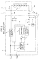
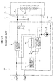
- a vehicular lamp lighting circuit is known with a configuration that comprises a control unit 2 and a light emitting diode (LED) unit, i.e., a light source unit, 10, such as is depicted in Fig. 1 , wherein the light emitting diode (LED) unit 10 is configured from an array of a plurality of an LED 9, and the control unit 2, which is broadly configured from a voltage boosting circuit 4, a reference voltage circuit 5, an amplifier 6, a voltage detection circuit 7, and a constant current circuit 8, performs a control of a turning on of electricity to the light emitting diode (LED) unit 10; refer, for instance, to Japanese Patent Laid Open No. 2003-187614 .
- LED light emitting diode
- the minus terminal harness 10b is caught by something and shorts out in a ground (GND), then, as is depicted in Fig. 2 , the current IF flows, the detected voltage V1 that arises at both ends of the output current detected resistor R1 effectively falls to zero, causing the control voltage V3 to be reduced, whereupon the difference arises between the reference voltage of the reference voltage circuit 5 and the control voltage V3, within the voltage boosting control IC, and, in order to reduce the difference within the voltage boosting control IC, the control acts in the direction that increases the duty ratio of the transistor of the voltage boosting circuit 4, and the output voltage V2 is boosted, and repeating the control thereof over a plurality of instances gradually boosts the output voltage V2, increasing the current IF, such that the current IF that flows to the LED 9 significantly exceeds the constant current, and the light emitting diode (LED) unit 10 is destroyed as a result.
- GND ground
- the control acts in the direction that increases the duty ratio of the transistor of the voltage boosting circuit 4, and the output voltage V2 is boosted, and thus, the output voltage V2 is gradually boosted, increasing the current IF: and, while almost all of the current IF is going to ground (GND), thereby avoiding the destruction of the light emitting diode (LED) unit 10, repeating the control thereof over a plurality of instances causes the control unit 2 itself to be burnt out
- the present invention was devised with the foregoing circumstance in mind, and has as an objective to provide a vehicular lamp lighting circuit that is capable of preventing the burning out of the control unit, or the destruction of the light source unit, even when the harness that is connected to the light source unit shorts out.
- An aspect of the present invention relates to a vehicular lamp lighting circuit including a control unit configured to control an electric current that flows to a light source unit having an electric current supply section configured to output the electric current to the light source unit, a switching controller configured to compare, with a reference voltage, and to control, by switching, the electric current that is outputted from the electric current supply section, an output current detection section configured to detect the electric current that flows into the light source unit, and a voltage transform circuit configured to transform an electric potential difference that arises from the electric current that flows into the output current detection section into a difference voltage and to output the difference voltage thus converted to the switching controller; wherein the output current detection section is connected to a high electric potential side of the light source unit, and the switching controller compares the reference voltage with the difference voltage and controls the electric current supply section so as to reduce the difference therebetween.
- the output current detection section is a resistor for detection of an output current.
- the light source unit is formed from an array in which a plurality of light emitting diode (LED) is connected in a series, the high electric potential side of the light source unit is connected to the resistor for detection of the output current via a plus terminal harness, and a low electric potential side of the light source unit is connected to a ground via a minus terminal harness.
- LED light emitting diode
- a connector comprising a plurality of connector pins, is installed between the control unit and the light source unit, the light source unit is selectively connected to one of the plurality of connector pins, and the electric current that flows to the light source unit is selectable.
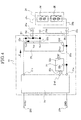
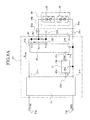
- Fig. 4 describes a first embodiment of a vehicular lamp lighting circuit according to the present invention
- reference numeral 20 in Fig. 4 is a control unit.
- the control unit 20 comprises a switching regulator 21 as a current supply section, a switching controller 22, and a voltage transform circuit 23.
- the switching regulator 21 includes a power supply terminal 21a and a ground (GND) terminal 21b on a power supply side thereof, and an output terminal 21c, a control terminal 21d, and a ground (GND) terminal 21e on an output side thereof.
- GND ground
- a power supply voltage Vin is applied to the power supply terminal 21a from a battery (not shown), for instance, and the ground (GND) terminal 21b is grounded.
- the output terminal 21c is connected to one terminal of a resistor for detection of an output current as an output current detection unit R1, and to an input terminal 23a of the voltage transform circuit 23.
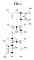
- the voltage transform circuit 23 is configured from transistors Tr1 to Tr4, and resistors Rs1 to Rs6, such as is depicted in Fig. 5 , for instance.
- the voltage transform circuit 23 further includes an input terminal 23b and a control terminal 23c.
- the control terminal 21d of the switching regulator 21 is connected to an output terminal 22a of the switching controller 22.
- a difference voltage V3 is inputted from the control terminal 23c of the voltage transform circuit 23 into an input terminal 22b of the switching controller 22.
- the switching controller 22 compares the difference voltage V3 with a reference voltage VREF, and outputs a voltage VD, which corresponds to a difference therebetween to the control terminal 21d, whereupon the switching regulator 21 outputs a current IF such that the difference therebetween goes to zero.
- the other terminal of the resistor for detection of the output current R1 is connected via a plus terminal harness 24a to a high electric potential side of a light emitting diode (LED) unit 24 via a connection terminal, i.e., a connecting pin, 25a of a connector 25, and is also connected to one terminal of an unused resistor for detection of an output current R2.
- the other terminal of the unused resistor for detection of the output current R2 is connected to the input terminal 23b of the voltage transform circuit 23, and is also connected to a connection terminal, i.e., a connecting pin, 25b of the connector 25.
- the connection terminal, i.e., the connecting pin, 25b is open.
- the light emitting diode (LED) unit 24 is formed from an array of an LED element 26, and a low electric potential terminal of the light emitting diode (LED) unit 24 is connected to a ground (GND) terminal, i.e., a ground (GND) connecting pin, 25c of the connector 25, via a minus side harness 24b.
- the ground (GND) terminal 25c is connected to a ground (GND) terminal 23d of the voltage transform circuit 23, a ground (GND) terminal 22c of the switching controller 22, and the ground (GND) terminal 21e of the switching regulator 21.
- the voltage transform circuit 23 treats an electric potential of the input terminal 23a as Va1, treats an electric potential of the input terminal 23b as Va2, and outputs a voltage Va3, which is equivalent to a difference of Va1 - Va2, from the control terminal 23c to the input terminal 22b.
- the switching regulator 21 controls the light emitting diode (LED) unit 24 such that a voltage that flows through both terminals thereof is the reference voltage VREF, by the current IF flowing into the resistor for detection of the output current R1. Put another way, the current that flows to the light emitting diode (LED) unit 24 is controlled by the resistor for detection of the output current R1.
- the switching regulator 21 is controlled by the switching controller 22 and the current IF flows to the light emitting diode (LED) unit 24, such that the difference voltage (Va1 - Va2) is equivalent to the reference voltage VREF.
- the plus terminal harness 24a shorts out into the ground (GND) for some reason or other, such as is depicted in Fig. 7 , the electric potential of the plus terminal harness 24a goes to zero volts. Accordingly, the electric potential Va3 of the input terminal 23b goes to zero volts. The current IF, however, continues to flow through the resistor for detection of the output current R1, and thus, the electric potential Va1 that is inputted into the input terminal 23b is greater than zero volts. Accordingly, the difference voltage Va3 is also greater than zero volts.
- the difference voltage Va3 is equivalent to an electric potential difference (Va1 - Va2) that arises as a result of a current flowing that possesses a current value different from a current value of the current IF.
- the switching regulator 21 continues supplying the current IF to the light emitting diode (LED) unit 24 and the ground (GND) in the state wherein the plus terminal harness 24a shorts out into the ground (GND)
- the increase of the current IF is interrupted at a point in time when the difference voltage Va3 becomes equivalent to the reference voltage VREF, such that, accordingly, a circuit operation of the switching regulator 21 is stable, and a burnout or a destruction of the switching regulator 21 is prevented thereby.
- a configuration is presumed wherein the plus terminal harness 24a, such as is depicted in Fig. 8B is connected to the connection terminal 25b is in the open state, such as is depicted in Fig. 8A .
- the current IF is determined by the resistance value of the resistor for detection of the output current R1 and the resistance value of the resistor for detection of the output current R2.
- the switching controller 22 adjusts the current IF of the switching regulator 21 such that the voltage of the reference voltage VREF is 1.0 volts. Put another way, the current IF is adjusted such that the voltage V3 is the reference voltage VREF, i.e., 1.0 volts.
- the control is executed in a manner similar to the control that is executed according to the first embodiment when the plus terminal harness 24a shorts out into the ground (GND) for some reason or other, even when the plus terminal harness 24a is connected to the connection terminal 25b. Therefore, the burning out and the destruction of the circuit of the switching regulator 21 are prevented.
- an effect is demonstrated of being capable of preventing the burning out of the control circuit, or the destruction of the light source unit, even when the harness that is connected to the light source unit shorts out.
Landscapes
- Lighting Device Outwards From Vehicle And Optical Signal (AREA)
- Circuit Arrangement For Electric Light Sources In General (AREA)
Applications Claiming Priority (1)
| Application Number | Priority Date | Filing Date | Title |
|---|---|---|---|
| JP2007090528A JP2008251320A (ja) | 2007-03-30 | 2007-03-30 | 車両用灯具点灯回路 |
Publications (2)
| Publication Number | Publication Date |
|---|---|
| EP1976339A2 true EP1976339A2 (de) | 2008-10-01 |
| EP1976339A3 EP1976339A3 (de) | 2013-05-29 |
Family
ID=39577519
Family Applications (1)
| Application Number | Title | Priority Date | Filing Date |
|---|---|---|---|
| EP08153452.1A Withdrawn EP1976339A3 (de) | 2007-03-30 | 2008-03-27 | Beleuchtungsschaltung einer Fahrzeuglampe |
Country Status (3)
| Country | Link |
|---|---|
| US (1) | US7642723B2 (de) |
| EP (1) | EP1976339A3 (de) |
| JP (1) | JP2008251320A (de) |
Cited By (2)
| Publication number | Priority date | Publication date | Assignee | Title |
|---|---|---|---|---|
| ITCO20130003A1 (it) * | 2013-02-04 | 2013-05-06 | Gianantonio Moretto | Apparato per la rilevazione di lampade guaste in un sistema veicolare universale con installazione non invasiva |
| CN104396347A (zh) * | 2012-06-11 | 2015-03-04 | 株式会社Elm | 高稳定调光装置 |
Families Citing this family (4)
| Publication number | Priority date | Publication date | Assignee | Title |
|---|---|---|---|---|
| JP4457312B2 (ja) * | 2006-01-12 | 2010-04-28 | 株式会社デンソー | 車両用ヘッドランプ装置 |
| US8405325B2 (en) | 2008-10-30 | 2013-03-26 | Mitsubishi Electric Corporation | LED lighting power source and LED lighting system |
| DE102015219903B4 (de) * | 2015-10-14 | 2017-11-16 | Continental Automotive Gmbh | Verfahren und Schaltungsvorrichtung zum Detektieren eines Ausfalls zumindest einer Leuchtdiode in einer Leuchtdiodenanordnung |
| DE102018132077A1 (de) * | 2018-12-13 | 2020-06-18 | HELLA GmbH & Co. KGaA | Schaltungsanordnung und Verfahren zur Erkennung eines Kurzschlusses in einer Leuchteinheit |
Citations (1)
| Publication number | Priority date | Publication date | Assignee | Title |
|---|---|---|---|---|
| JP2003187614A (ja) | 2001-12-19 | 2003-07-04 | Toyoda Gosei Co Ltd | 車両用リアコンビネーションランプ装置 |
Family Cites Families (5)
| Publication number | Priority date | Publication date | Assignee | Title |
|---|---|---|---|---|
| JP4148908B2 (ja) * | 2004-02-16 | 2008-09-10 | 株式会社小糸製作所 | 車両用灯具 |
| JP4771354B2 (ja) * | 2004-09-17 | 2011-09-14 | 株式会社小糸製作所 | 車両用灯具の点灯制御回路 |
| JP4400880B2 (ja) * | 2004-10-05 | 2010-01-20 | 株式会社小糸製作所 | 車両用灯具の点灯制御回路 |
| JP2006210219A (ja) * | 2005-01-31 | 2006-08-10 | Koito Mfg Co Ltd | 車両用灯具の点灯制御回路 |
| JP4398411B2 (ja) * | 2005-07-12 | 2010-01-13 | 株式会社小糸製作所 | 車両用灯具の点灯制御装置 |
-
2007
- 2007-03-30 JP JP2007090528A patent/JP2008251320A/ja active Pending
-
2008
- 2008-03-27 EP EP08153452.1A patent/EP1976339A3/de not_active Withdrawn
- 2008-03-28 US US12/058,015 patent/US7642723B2/en not_active Expired - Fee Related
Patent Citations (1)
| Publication number | Priority date | Publication date | Assignee | Title |
|---|---|---|---|---|
| JP2003187614A (ja) | 2001-12-19 | 2003-07-04 | Toyoda Gosei Co Ltd | 車両用リアコンビネーションランプ装置 |
Cited By (2)
| Publication number | Priority date | Publication date | Assignee | Title |
|---|---|---|---|---|
| CN104396347A (zh) * | 2012-06-11 | 2015-03-04 | 株式会社Elm | 高稳定调光装置 |
| ITCO20130003A1 (it) * | 2013-02-04 | 2013-05-06 | Gianantonio Moretto | Apparato per la rilevazione di lampade guaste in un sistema veicolare universale con installazione non invasiva |
Also Published As
| Publication number | Publication date |
|---|---|
| EP1976339A3 (de) | 2013-05-29 |
| JP2008251320A (ja) | 2008-10-16 |
| US7642723B2 (en) | 2010-01-05 |
| US20080238324A1 (en) | 2008-10-02 |
Similar Documents
| Publication | Publication Date | Title |
|---|---|---|
| US8536800B2 (en) | Illuminating device and controlling method thereof | |
| JP4907078B2 (ja) | 発光ダイオード用電気供給装置および同装置を有するランプ | |
| EP1976339A2 (de) | Beleuchtungsschaltung einer Fahrzeuglampe | |
| US10360969B2 (en) | Light emitting element driving semiconductor integrated circuit, light emitting element driving device, light emitting device, and vehicle | |
| US20080197789A1 (en) | Light emitting device | |
| JP5603160B2 (ja) | 半導体光源点灯回路および制御方法 | |
| CN107757476B (zh) | 点灯电路以及车辆用灯具 | |
| JP6821835B2 (ja) | 点灯回路およびそれを用いた車両用灯具 | |
| JP2004322982A (ja) | 車両用灯具 | |
| CN111034043B (zh) | 通电控制装置 | |
| US7902758B2 (en) | Power supply system and method for automotive LED lighting systems | |
| KR20040084729A (ko) | 조명장치와 그것에 사용하는 조명헤드 및 전원장치 | |
| US7986106B2 (en) | Protection circuit and discharge lamp driving device employing the same | |
| JP2008283206A (ja) | Led点灯装置 | |
| DE602006004497D1 (de) | Lastschutzschaltung und Schaltungsanordnung für Gasentladungslampe | |
| JP4082547B2 (ja) | 発光素子の電源供給制御装置 | |
| JP7408448B2 (ja) | 光源モジュールおよび点灯回路 | |
| JP2007004995A (ja) | Led点灯装置 | |
| KR20140017212A (ko) | 발광다이오드 구동 회로 | |
| JP5210254B2 (ja) | 光源装置、光源装置の制御方法 | |
| US10602579B2 (en) | Method for regulating an operating current of a lighting unit and control device and motor vehicle | |
| WO2019233969A1 (en) | A led driver and a led module for use with the driver | |
| JP4506593B2 (ja) | 照明装置 | |
| US11382194B2 (en) | Lighting circuit | |
| JP2008218457A (ja) | Led車両用灯具の調光回路 |
Legal Events
| Date | Code | Title | Description |
|---|---|---|---|
| PUAI | Public reference made under article 153(3) epc to a published international application that has entered the european phase |
Free format text: ORIGINAL CODE: 0009012 |
|
| AK | Designated contracting states |
Kind code of ref document: A2 Designated state(s): AT BE BG CH CY CZ DE DK EE ES FI FR GB GR HR HU IE IS IT LI LT LU LV MC MT NL NO PL PT RO SE SI SK TR |
|
| AX | Request for extension of the european patent |
Extension state: AL BA MK RS |
|
| PUAL | Search report despatched |
Free format text: ORIGINAL CODE: 0009013 |
|
| AK | Designated contracting states |
Kind code of ref document: A3 Designated state(s): AT BE BG CH CY CZ DE DK EE ES FI FR GB GR HR HU IE IS IT LI LT LU LV MC MT NL NO PL PT RO SE SI SK TR |
|
| AX | Request for extension of the european patent |
Extension state: AL BA MK RS |
|
| RIC1 | Information provided on ipc code assigned before grant |
Ipc: H05B 33/08 20060101AFI20130419BHEP Ipc: F21S 8/10 20060101ALI20130419BHEP |
|
| AKY | No designation fees paid | ||
| REG | Reference to a national code |
Ref country code: DE Ref legal event code: R108 |
|
| REG | Reference to a national code |
Ref country code: DE Ref legal event code: R108 Effective date: 20140205 |
|
| STAA | Information on the status of an ep patent application or granted ep patent |
Free format text: STATUS: THE APPLICATION IS DEEMED TO BE WITHDRAWN |
|
| 18D | Application deemed to be withdrawn |
Effective date: 20131001 |