EP1974921B1 - Self Aligned Port Hole Opening Process for Ink Jet Print Heads - Google Patents
Self Aligned Port Hole Opening Process for Ink Jet Print Heads Download PDFInfo
- Publication number
- EP1974921B1 EP1974921B1 EP08151999.3A EP08151999A EP1974921B1 EP 1974921 B1 EP1974921 B1 EP 1974921B1 EP 08151999 A EP08151999 A EP 08151999A EP 1974921 B1 EP1974921 B1 EP 1974921B1
- Authority
- EP
- European Patent Office
- Prior art keywords
- jet stack
- port holes
- polymer
- ink
- planarized
- Prior art date
- Legal status (The legal status is an assumption and is not a legal conclusion. Google has not performed a legal analysis and makes no representation as to the accuracy of the status listed.)
- Ceased
Links
Images


Classifications
-
- B—PERFORMING OPERATIONS; TRANSPORTING
- B41—PRINTING; LINING MACHINES; TYPEWRITERS; STAMPS
- B41J—TYPEWRITERS; SELECTIVE PRINTING MECHANISMS, i.e. MECHANISMS PRINTING OTHERWISE THAN FROM A FORME; CORRECTION OF TYPOGRAPHICAL ERRORS
- B41J2/00—Typewriters or selective printing mechanisms characterised by the printing or marking process for which they are designed
- B41J2/005—Typewriters or selective printing mechanisms characterised by the printing or marking process for which they are designed characterised by bringing liquid or particles selectively into contact with a printing material
- B41J2/01—Ink jet
- B41J2/135—Nozzles
- B41J2/14—Structure thereof only for on-demand ink jet heads
- B41J2/14201—Structure of print heads with piezoelectric elements
- B41J2/14233—Structure of print heads with piezoelectric elements of film type, deformed by bending and disposed on a diaphragm
-
- B—PERFORMING OPERATIONS; TRANSPORTING
- B41—PRINTING; LINING MACHINES; TYPEWRITERS; STAMPS
- B41J—TYPEWRITERS; SELECTIVE PRINTING MECHANISMS, i.e. MECHANISMS PRINTING OTHERWISE THAN FROM A FORME; CORRECTION OF TYPOGRAPHICAL ERRORS
- B41J2/00—Typewriters or selective printing mechanisms characterised by the printing or marking process for which they are designed
- B41J2/22—Typewriters or selective printing mechanisms characterised by the printing or marking process for which they are designed characterised by selective application of impact or pressure on a printing material or impression-transfer material
- B41J2/23—Typewriters or selective printing mechanisms characterised by the printing or marking process for which they are designed characterised by selective application of impact or pressure on a printing material or impression-transfer material using print wires
- B41J2/235—Print head assemblies
-
- B—PERFORMING OPERATIONS; TRANSPORTING
- B41—PRINTING; LINING MACHINES; TYPEWRITERS; STAMPS
- B41J—TYPEWRITERS; SELECTIVE PRINTING MECHANISMS, i.e. MECHANISMS PRINTING OTHERWISE THAN FROM A FORME; CORRECTION OF TYPOGRAPHICAL ERRORS
- B41J2/00—Typewriters or selective printing mechanisms characterised by the printing or marking process for which they are designed
- B41J2/005—Typewriters or selective printing mechanisms characterised by the printing or marking process for which they are designed characterised by bringing liquid or particles selectively into contact with a printing material
- B41J2/01—Ink jet
- B41J2/015—Ink jet characterised by the jet generation process
- B41J2/04—Ink jet characterised by the jet generation process generating single droplets or particles on demand
- B41J2/045—Ink jet characterised by the jet generation process generating single droplets or particles on demand by pressure, e.g. electromechanical transducers
-
- B—PERFORMING OPERATIONS; TRANSPORTING
- B41—PRINTING; LINING MACHINES; TYPEWRITERS; STAMPS
- B41J—TYPEWRITERS; SELECTIVE PRINTING MECHANISMS, i.e. MECHANISMS PRINTING OTHERWISE THAN FROM A FORME; CORRECTION OF TYPOGRAPHICAL ERRORS
- B41J2/00—Typewriters or selective printing mechanisms characterised by the printing or marking process for which they are designed
- B41J2/005—Typewriters or selective printing mechanisms characterised by the printing or marking process for which they are designed characterised by bringing liquid or particles selectively into contact with a printing material
- B41J2/01—Ink jet
- B41J2/135—Nozzles
- B41J2/16—Production of nozzles
- B41J2/1607—Production of print heads with piezoelectric elements
- B41J2/161—Production of print heads with piezoelectric elements of film type, deformed by bending and disposed on a diaphragm
-
- B—PERFORMING OPERATIONS; TRANSPORTING
- B41—PRINTING; LINING MACHINES; TYPEWRITERS; STAMPS
- B41J—TYPEWRITERS; SELECTIVE PRINTING MECHANISMS, i.e. MECHANISMS PRINTING OTHERWISE THAN FROM A FORME; CORRECTION OF TYPOGRAPHICAL ERRORS
- B41J2/00—Typewriters or selective printing mechanisms characterised by the printing or marking process for which they are designed
- B41J2/005—Typewriters or selective printing mechanisms characterised by the printing or marking process for which they are designed characterised by bringing liquid or particles selectively into contact with a printing material
- B41J2/01—Ink jet
- B41J2/135—Nozzles
- B41J2/16—Production of nozzles
- B41J2/1621—Manufacturing processes
- B41J2/1623—Manufacturing processes bonding and adhesion
-
- B—PERFORMING OPERATIONS; TRANSPORTING
- B41—PRINTING; LINING MACHINES; TYPEWRITERS; STAMPS
- B41J—TYPEWRITERS; SELECTIVE PRINTING MECHANISMS, i.e. MECHANISMS PRINTING OTHERWISE THAN FROM A FORME; CORRECTION OF TYPOGRAPHICAL ERRORS
- B41J2/00—Typewriters or selective printing mechanisms characterised by the printing or marking process for which they are designed
- B41J2/005—Typewriters or selective printing mechanisms characterised by the printing or marking process for which they are designed characterised by bringing liquid or particles selectively into contact with a printing material
- B41J2/01—Ink jet
- B41J2/135—Nozzles
- B41J2/16—Production of nozzles
- B41J2/1621—Manufacturing processes
- B41J2/1626—Manufacturing processes etching
-
- B—PERFORMING OPERATIONS; TRANSPORTING
- B41—PRINTING; LINING MACHINES; TYPEWRITERS; STAMPS
- B41J—TYPEWRITERS; SELECTIVE PRINTING MECHANISMS, i.e. MECHANISMS PRINTING OTHERWISE THAN FROM A FORME; CORRECTION OF TYPOGRAPHICAL ERRORS
- B41J2/00—Typewriters or selective printing mechanisms characterised by the printing or marking process for which they are designed
- B41J2/005—Typewriters or selective printing mechanisms characterised by the printing or marking process for which they are designed characterised by bringing liquid or particles selectively into contact with a printing material
- B41J2/01—Ink jet
- B41J2/135—Nozzles
- B41J2/16—Production of nozzles
- B41J2/1621—Manufacturing processes
- B41J2/1632—Manufacturing processes machining
- B41J2/1634—Manufacturing processes machining laser machining
-
- Y—GENERAL TAGGING OF NEW TECHNOLOGICAL DEVELOPMENTS; GENERAL TAGGING OF CROSS-SECTIONAL TECHNOLOGIES SPANNING OVER SEVERAL SECTIONS OF THE IPC; TECHNICAL SUBJECTS COVERED BY FORMER USPC CROSS-REFERENCE ART COLLECTIONS [XRACs] AND DIGESTS
- Y10—TECHNICAL SUBJECTS COVERED BY FORMER USPC
- Y10T—TECHNICAL SUBJECTS COVERED BY FORMER US CLASSIFICATION
- Y10T156/00—Adhesive bonding and miscellaneous chemical manufacture
- Y10T156/10—Methods of surface bonding and/or assembly therefor
Definitions
- the numerical values as stated for the parameter can take on negative values, In this case, the example value of range stated as "less that 10" can assume negative values, e.g. - 1, -2, -3, - 10, -20, -30, etc.
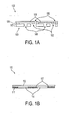
- the partial jet stack 102 can include a brazed three layer stainless steel structure including the diaphragm 104, the body plate 105, and the inlet plate 107.
- the partial jet stack 102 can include port holes 106 formed, for example, by chemical etching.
- the planarized polymer 117 can be selected from at least one of epoxy, polyimide, and silicone. In some embodiments, the planarized polymer 117 can have a tensile modulus less than about 2 GPa at about 120 °C. In some embodiments, the piezoelectric elements 114 and the planarized polymer 117 can have a thickness from about 10 ⁇ m to about 100 ⁇ m. In various embodiments, the step of providing a piezoelectric array 115 can further include providing the plurality of piezoelectric elements 114 disposed in an array on a carrier 112, as shown in FIG. 1B .
- the carrier 112 can be a metal support layer including one or more of a pressure sensitive adhesive and a releasable adhesive to hold the piezoelectric elements 114 to the carrier.
- the step of providing the piezoelectric array 115 can include providing a piezoelectric sheet bonded to a carrier 112, cutting or slicing the piezoelectric sheet to form a plurality of kerfed regions 216, as shown in FIG. 2B , filling the kerfed regions 216 with a polymer, and planarizing the polymer in the kerfed region to form a plurality of piezoelectric elements 114 disposed in a planarized polymer 117 as shown in FIGS. 1B and 2C .
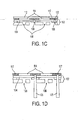
- the method of making an ink jet print head 100 can further include bonding the piezoelectric array 115 to a side opposite to the ink outlet side 109 of the partial jet stack 102, wherein the partial jet stack 102 can be aligned such that the planarized polymer 117 can cover the plurality of port holes 106 as shown in FIG. 1C .
- the bonding of the piezoelectric array 115 to the partial jet stack 102 can done using an adhesive 122 including but not limited to, for example epoxy, silicone, and bismaleimide.
- the adhesive 122 can be dispensed on the partial jet stack 102. In other embodiments, the adhesive 122 can be dispensed on the piezoelectric array 115.
- the method of making an ink jet print head 100 can also include using the partial jet stack 102 as a mask to extend the port holes 106 through the planarized polymer 117 by ablating the planarized polymer 117 from the ink outlet side 109 using a laser beam 125, generated by a laser, as shown in FIG. 1D .
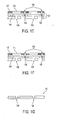
- the extended port hole 166 through the planarized polymer 117 formed by laser ablation can have a uniform cross-section as shown in FIG. 1E .
- the extended port hole 166 through the planarized polymer 117 formed by laser ablation can have a tapered cross-section as shown in FIG. 1F .
- ablating the planarized polymer 117 from the ink outlet side 109 can include using at least one of a CO 2 laser, an excimer laser, a solid state laser, a copper vapor laser, and a fiber laser.
- a CO 2 laser can typically ablate polymers including epoxies.
- the CO 2 laser can have a low operating cost and can be ideal for high volume production.
- the CO 2 laser beam that can over-fill the mask could sequentially illuminate each port hole 106 to form the extended port holes 166 through the polymer 117 and remove an excess portion of the adhesive 122 that flows into the port hole 106 from the bonding of the piezoelectric array 115 to the partial jet stack 102, as shown in FIGS. 1E and 1F .
- the excimer laser can be used to flood illuminate or can be used with special optics to illuminate each of the port holes 106 to form the extended port holes 166 though the polymer 117 and remove an excess portion of the adhesive 122 from the bonding of the piezoelectric array 115 to the partial jet stack 102, as shown in FIGS. 1E and 1F .
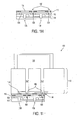
- the method of making an ink jet print head 100 can further include bonding an aperture plate 130 as shown in FIG. 1G including a second plurality of outlet apertures 138 to the ink outlet side 109 of the partial jet stack 102, wherein the second plurality of outlet apertures 138 are substantially aligned with the first plurality of outlet apertures 108 as shown in FIG. 1H .
- an adhesive such as a thermoplastic polyimide can be used in bonding the aperture plate 130 to the partial jet stack 102.
- a b-staged epoxy can used in bonding the aperture plate 130 to the partial jet stack 102.
- the aperture plate 130 can include a single layer or a two layer metal structure.
- the aperture plate 130 can be formed of stainless steel.
- the aperture plate 130 can include a polymeric plate wherein the second plurality of outlet apertures 138 can be formed by laser ablation.
- the aperture plate 130 can include polymers such as polyimide, polyetherimide, polysulfone, polyetherketone, polyphenylene sulfide, and polyester.
- the method of making an ink jet print head 100 can further include bonding filters, manifolds, other jet stack design elements to the partial jet stack 102, circuit board 140, and flexible circuit substrates.
- the standoff layer 146 can include acrylic polymer. In other embodiments, the standoff layer 146 can include silicone. In certain embodiments, the standoff layer 146 can be precut having an adhesive portion that can be aligned and bonded with heat treatment.
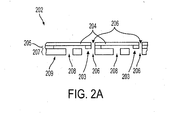
- the method of making a jet stack 200 can include providing a partial jet stack 202 including a diaphragm 204, a plurality of port holes 206, a plurality of inlet channels and a first plurality of out let apertures 208, and having an ink outlet side 209, as shown in FIG. 2A .
- the method of making a jet stack 200 can also include providing a piezoelectric array 210 on a carrier 212 including a plurality of piezoelectric elements 214 and a plurality of kerfed regions 216, as shown in FIG. 2B .
- each of the kerfed regions can be wide enough to accommodate the port holes 106. In some embodiments, each of the kerfed regions can have width in the range of about 100 ⁇ m to about 400 ⁇ m.
- the method of making a jet stack 200 can further include depositing a polymer 217 in the kerfed regions 116 and planarizing the polymer 217 in the kerfed regions 216 to form a polymer planarized piezoelectric array 215, as shown in FIG. 2C .
- the kerfed regions 216 can be filled with a prepolymer liquid or paste, which can then be polymerized.
- the method of making a jet stack 200 can also include bonding the polymer planarized piezoelectric array 215 to a side opposite to the ink outlet side 209 of the partial jet stack 202 using an adhesive 222, wherein the partial jet stack 202 is aligned such that the planarized polymer 217 covers the plurality of port holes 206, as shown in FIG. 2D .
- the adhesive 222 forms a thin layer between the partial jet stack 202 and the polymer planarized piezoelectric array 215, with an excess portion of the adhesive 222 flowing into the port hole 206 from the bonding of the piezoelectric array 215 to the partial jet stack 202.
- the method of making a jet stack 200 can further include using the partial jet stack 202 as a mask to extend the port holes 206 through the polymer 217 by ablating the polymer 217 and an excess portion of the adhesive 222 from the ink outlet side 209 using a laser beam 225, generated by a laser, as shown in FIG. 2E .
- the step of ablating the planarized polymer 217 from the ink outlet side 209 can include using at least one of a CO 2 laser, an excimer laser, a solid state laser, a copper vapor laser, and a fiber laser.
- the method of making a jet stack 200 can include the providing a partial jet stack 202 including four layers or less.
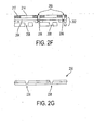
- the method of making a jet stack 200 can also include cleaning the extended port holes 266 through the planarized polymer 217 to remove any debris from the ablation of the planarized polymer 217 and the adhesive, as shown in FIG. 2G and bonding an aperture plate 230 as shown in FIG. 2G including a second plurality of outlet apertures 238 to the ink outlet side 209 of the partial jet stack 202 as shown in FIG. 2H , wherein the second plurality of outlet apertures 238 can be substantially aligned with the first plurality of outlet apertures 208.
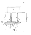
- the ink jet print head 300 can further include an aperture plate 330 including a second plurality of outlet apertures 338 bonded to the inlet plate 307 of the partial jet stack 302, wherein the second plurality of outlet apertures 338 are substantially aligned with the first plurality of outlet apertures 308.
- the ink jet print head 300 can also include a circuit board 340 including a plurality of vias 342, a plurality of contact pads 344, and a plurality of electrical connections 345 bonded to the piezoelectric array 315 with a standoff layer 346, wherein the standoff layer 346 provides a fluid seal between the circuit board 340 and the plurality of port holes 306.
Landscapes
- Engineering & Computer Science (AREA)
- Manufacturing & Machinery (AREA)
- Physics & Mathematics (AREA)
- Optics & Photonics (AREA)
- Particle Formation And Scattering Control In Inkjet Printers (AREA)
Applications Claiming Priority (1)
| Application Number | Priority Date | Filing Date | Title |
|---|---|---|---|
| US11/692,616 US7959266B2 (en) | 2007-03-28 | 2007-03-28 | Self aligned port hole opening process for ink jet print heads |
Publications (2)
| Publication Number | Publication Date |
|---|---|
| EP1974921A1 EP1974921A1 (en) | 2008-10-01 |
| EP1974921B1 true EP1974921B1 (en) | 2014-01-22 |
Family
ID=39484546
Family Applications (1)
| Application Number | Title | Priority Date | Filing Date |
|---|---|---|---|
| EP08151999.3A Ceased EP1974921B1 (en) | 2007-03-28 | 2008-02-27 | Self Aligned Port Hole Opening Process for Ink Jet Print Heads |
Country Status (7)
| Country | Link |
|---|---|
| US (1) | US7959266B2 (enExample) |
| EP (1) | EP1974921B1 (enExample) |
| JP (1) | JP4981725B2 (enExample) |
| KR (1) | KR101440784B1 (enExample) |
| CN (2) | CN101274523B (enExample) |
| BR (1) | BRPI0800929A2 (enExample) |
| MX (1) | MX2008003916A (enExample) |
Families Citing this family (22)
| Publication number | Priority date | Publication date | Assignee | Title |
|---|---|---|---|---|
| US7448734B2 (en) * | 2004-01-21 | 2008-11-11 | Silverbrook Research Pty Ltd | Inkjet printer cartridge with pagewidth printhead |
| US8360557B2 (en) * | 2008-12-05 | 2013-01-29 | Xerox Corporation | Method for laser drilling fluid ports in multiple layers |
| US8240818B2 (en) | 2009-12-17 | 2012-08-14 | Xerox Corporation | Inkjet ejector having a polymer aperture plate attached to an outlet plate and method for assembling an inkjet ejector |
| US8297742B2 (en) * | 2010-03-19 | 2012-10-30 | Fujifilm Corporation | Bonded circuits and seals in a printing device |
| JP5943590B2 (ja) * | 2011-01-07 | 2016-07-05 | 日本発條株式会社 | 圧電素子の製造方法、圧電素子、圧電アクチュエータ、及びヘッド・サスペンション |
| US8465659B2 (en) | 2011-01-21 | 2013-06-18 | Xerox Corporation | Polymer layer removal on pzt arrays using a plasma etch |
| US8585183B2 (en) * | 2011-03-22 | 2013-11-19 | Xerox Corporation | High density multilayer interconnect for print head |
| US8550601B2 (en) | 2011-03-23 | 2013-10-08 | Xerox Corporation | Use of photoresist material as an interstitial fill for PZT printhead fabrication |
| US8567924B2 (en) | 2011-04-07 | 2013-10-29 | Xerox Corporation | Patterned conductive array and self leveling epoxy |
| US8585187B2 (en) * | 2011-04-29 | 2013-11-19 | Xerox Corporation | High density electrical interconnect for printing devices using flex circuits and dielectric underfill |
| WO2013015814A1 (en) | 2011-07-28 | 2013-01-31 | Hewlett-Packard Development Company, L.P. | Adhesive transfer |
| US8585185B2 (en) * | 2011-09-22 | 2013-11-19 | Xerox Corporation | High density electrical interconnect using limited density flex circuits |
| US8794743B2 (en) * | 2011-11-30 | 2014-08-05 | Xerox Corporation | Multi-film adhesive design for interfacial bonding printhead structures |
| US8814328B2 (en) * | 2011-12-13 | 2014-08-26 | Xerox Corporation | Polymer film as an interstitial fill for PZT printhead fabrication |
| US8980026B2 (en) * | 2012-09-28 | 2015-03-17 | Apple Inc. | Gap seals for electronic device structures |
| US8740357B1 (en) | 2013-02-05 | 2014-06-03 | Xerox Corporation | Method and structure for sealing fine fluid features in a printing device |
| US10821729B2 (en) | 2013-02-28 | 2020-11-03 | Hewlett-Packard Development Company, L.P. | Transfer molded fluid flow structure |
| US11426900B2 (en) * | 2013-02-28 | 2022-08-30 | Hewlett-Packard Development Company, L.P. | Molding a fluid flow structure |
| ES2747823T3 (es) | 2013-02-28 | 2020-03-11 | Hewlett Packard Development Co | Barra de impresión moldeada |
| US9724920B2 (en) | 2013-03-20 | 2017-08-08 | Hewlett-Packard Development Company, L.P. | Molded die slivers with exposed front and back surfaces |
| TWI572494B (zh) * | 2013-07-29 | 2017-03-01 | 惠普發展公司有限責任合夥企業 | 流體流動結構及製造流體流動結構中之流體通道之方法 |
| US10549386B2 (en) * | 2016-02-29 | 2020-02-04 | Xerox Corporation | Method for ablating openings in unsupported layers |
Family Cites Families (12)
| Publication number | Priority date | Publication date | Assignee | Title |
|---|---|---|---|---|
| JP3301485B2 (ja) | 1992-03-18 | 2002-07-15 | セイコーエプソン株式会社 | インクジェット式印字ヘッド及びその製造方法 |
| JP2001096746A (ja) * | 1999-10-01 | 2001-04-10 | Ricoh Co Ltd | インクジェット記録ヘッドおよびその製造方法 |
| WO2001042024A1 (en) | 1999-12-10 | 2001-06-14 | Fujitsu Limited | Ink jet head and printer |
| JP2001191540A (ja) * | 2000-01-06 | 2001-07-17 | Ricoh Co Ltd | ノズル形成部材及びその製造方法、インクジェットヘッド並びにインクジェット記録装置 |
| JP4221929B2 (ja) | 2000-03-31 | 2009-02-12 | 富士フイルム株式会社 | マルチノズルインクジエットヘッド |
| JP3603828B2 (ja) | 2001-05-28 | 2004-12-22 | 富士ゼロックス株式会社 | インクジェット式記録ヘッド及びその製造方法並びにインクジェット式記録装置 |
| JP2003145761A (ja) | 2001-08-28 | 2003-05-21 | Seiko Epson Corp | 液体噴射ヘッド及びその製造方法並びに液体噴射装置 |
| JP2006044222A (ja) * | 2004-06-11 | 2006-02-16 | Fuji Xerox Co Ltd | インクジェット記録ヘッド及びインクジェット記録装置 |
| JP2006044225A (ja) * | 2004-06-29 | 2006-02-16 | Fuji Xerox Co Ltd | 液滴吐出ヘッド及び液滴吐出装置 |
| US7549223B2 (en) * | 2004-09-28 | 2009-06-23 | Fujifilm Corporation | Method for manufacturing a liquid ejection head |
| US7524024B2 (en) | 2005-03-15 | 2009-04-28 | Fuji Xerox Co., Ltd. | Electrical connection substrate, droplet discharge head, and droplet discharge apparatus |
| JP2006326868A (ja) * | 2005-05-23 | 2006-12-07 | Brother Ind Ltd | 板状部材構造およびその製造方法 |
-
2007
- 2007-03-28 US US11/692,616 patent/US7959266B2/en active Active
-
2008
- 2008-02-27 EP EP08151999.3A patent/EP1974921B1/en not_active Ceased
- 2008-03-21 JP JP2008072730A patent/JP4981725B2/ja not_active Expired - Fee Related
- 2008-03-24 MX MX2008003916A patent/MX2008003916A/es active IP Right Grant
- 2008-03-27 CN CN200810087419XA patent/CN101274523B/zh not_active Expired - Fee Related
- 2008-03-27 CN CN201110239761.9A patent/CN102407669B/zh not_active Expired - Fee Related
- 2008-03-28 KR KR1020080028750A patent/KR101440784B1/ko not_active Expired - Fee Related
- 2008-03-28 BR BRPI0800929-5A patent/BRPI0800929A2/pt not_active IP Right Cessation
Also Published As
| Publication number | Publication date |
|---|---|
| KR101440784B1 (ko) | 2014-09-17 |
| US7959266B2 (en) | 2011-06-14 |
| CN102407669B (zh) | 2015-04-15 |
| EP1974921A1 (en) | 2008-10-01 |
| KR20080088485A (ko) | 2008-10-02 |
| MX2008003916A (es) | 2009-02-27 |
| JP2008238820A (ja) | 2008-10-09 |
| US20080239022A1 (en) | 2008-10-02 |
| CN101274523A (zh) | 2008-10-01 |
| CN102407669A (zh) | 2012-04-11 |
| CN101274523B (zh) | 2012-02-22 |
| JP4981725B2 (ja) | 2012-07-25 |
| BRPI0800929A2 (pt) | 2008-11-11 |
Similar Documents
| Publication | Publication Date | Title |
|---|---|---|
| EP1974921B1 (en) | Self Aligned Port Hole Opening Process for Ink Jet Print Heads | |
| EP0901906B1 (en) | Ink jet printhead with improved, laser-ablated filter | |
| KR101363562B1 (ko) | 액적 침착 장치 | |
| US6905202B2 (en) | Ink-jet head and recording apparatus | |
| US5818482A (en) | Ink jet printing head | |
| US9050802B2 (en) | Method for manufacturing liquid jetting apparatus, method for manufacturing nozzle plate, and liquid droplet jetting apparatus | |
| US20050179724A1 (en) | Droplet deposition apparatus | |
| US20040179057A1 (en) | Ink-jet printing head | |
| EP2013023B1 (en) | Printhead module | |
| US8733907B2 (en) | Liquid discharge head and method for manufacturing liquid discharge head | |
| JP2010201729A (ja) | 液体吐出ヘッド及びこれを含む記録装置の製造方法、並びに、液体吐出ヘッド及び記録装置 | |
| JP2006256006A (ja) | 液体噴射ヘッド | |
| JP3610987B2 (ja) | 積層型インクジェット式記録ヘッド | |
| US6592216B2 (en) | Ink jet print head acoustic filters | |
| JP3589108B2 (ja) | インクジェット式記録ヘッド及びインクジェット式記録装置 | |
| US8205969B2 (en) | Jet stack with precision port holes for ink jet printer and associated method | |
| JP6130308B2 (ja) | インクジェット式印字ヘッドを作成する方法 | |
| JP4049303B2 (ja) | インクジェット記録ヘッド | |
| JP2009202454A (ja) | 液滴吐出ヘッド及びその製造方法 | |
| JP2008126484A (ja) | インクジェットヘッドモジュールおよびその製造方法 | |
| JPH08118655A (ja) | インクジェット用ノズルプレート | |
| JP2019059078A (ja) | インクジェットヘッド、インクジェットヘッドの製造方法、および画像形成装置 | |
| JP2012086442A (ja) | インクジェットヘッドの製造方法 | |
| HK1126169B (en) | Printhead module |
Legal Events
| Date | Code | Title | Description |
|---|---|---|---|
| PUAI | Public reference made under article 153(3) epc to a published international application that has entered the european phase |
Free format text: ORIGINAL CODE: 0009012 |
|
| AK | Designated contracting states |
Kind code of ref document: A1 Designated state(s): AT BE BG CH CY CZ DE DK EE ES FI FR GB GR HR HU IE IS IT LI LT LU LV MC MT NL NO PL PT RO SE SI SK TR |
|
| AX | Request for extension of the european patent |
Extension state: AL BA MK RS |
|
| 17P | Request for examination filed |
Effective date: 20090401 |
|
| 17Q | First examination report despatched |
Effective date: 20090508 |
|
| AKX | Designation fees paid |
Designated state(s): DE FR GB |
|
| GRAP | Despatch of communication of intention to grant a patent |
Free format text: ORIGINAL CODE: EPIDOSNIGR1 |
|
| INTG | Intention to grant announced |
Effective date: 20131001 |
|
| GRAS | Grant fee paid |
Free format text: ORIGINAL CODE: EPIDOSNIGR3 |
|
| GRAA | (expected) grant |
Free format text: ORIGINAL CODE: 0009210 |
|
| AK | Designated contracting states |
Kind code of ref document: B1 Designated state(s): DE FR GB |
|
| REG | Reference to a national code |
Ref country code: GB Ref legal event code: FG4D |
|
| REG | Reference to a national code |
Ref country code: DE Ref legal event code: R096 Ref document number: 602008030043 Country of ref document: DE Effective date: 20140306 |
|
| REG | Reference to a national code |
Ref country code: DE Ref legal event code: R097 Ref document number: 602008030043 Country of ref document: DE |
|
| PLBE | No opposition filed within time limit |
Free format text: ORIGINAL CODE: 0009261 |
|
| STAA | Information on the status of an ep patent application or granted ep patent |
Free format text: STATUS: NO OPPOSITION FILED WITHIN TIME LIMIT |
|
| 26N | No opposition filed |
Effective date: 20141023 |
|
| REG | Reference to a national code |
Ref country code: DE Ref legal event code: R097 Ref document number: 602008030043 Country of ref document: DE Effective date: 20141023 |
|
| REG | Reference to a national code |
Ref country code: FR Ref legal event code: PLFP Year of fee payment: 9 |
|
| REG | Reference to a national code |
Ref country code: FR Ref legal event code: PLFP Year of fee payment: 10 |
|
| REG | Reference to a national code |
Ref country code: FR Ref legal event code: PLFP Year of fee payment: 11 |
|
| PGFP | Annual fee paid to national office [announced via postgrant information from national office to epo] |
Ref country code: GB Payment date: 20200123 Year of fee payment: 13 |
|
| PGFP | Annual fee paid to national office [announced via postgrant information from national office to epo] |
Ref country code: FR Payment date: 20200122 Year of fee payment: 13 |
|
| GBPC | Gb: european patent ceased through non-payment of renewal fee |
Effective date: 20210227 |
|
| PG25 | Lapsed in a contracting state [announced via postgrant information from national office to epo] |
Ref country code: GB Free format text: LAPSE BECAUSE OF NON-PAYMENT OF DUE FEES Effective date: 20210227 Ref country code: FR Free format text: LAPSE BECAUSE OF NON-PAYMENT OF DUE FEES Effective date: 20210228 |
|
| PGFP | Annual fee paid to national office [announced via postgrant information from national office to epo] |
Ref country code: DE Payment date: 20230119 Year of fee payment: 16 |
|
| REG | Reference to a national code |
Ref country code: DE Ref legal event code: R119 Ref document number: 602008030043 Country of ref document: DE |
|
| PG25 | Lapsed in a contracting state [announced via postgrant information from national office to epo] |
Ref country code: DE Free format text: LAPSE BECAUSE OF NON-PAYMENT OF DUE FEES Effective date: 20240903 |
|
| PG25 | Lapsed in a contracting state [announced via postgrant information from national office to epo] |
Ref country code: DE Free format text: LAPSE BECAUSE OF NON-PAYMENT OF DUE FEES Effective date: 20240903 |