EP1973069B1 - Halbleiterbauelement - Google Patents
Halbleiterbauelement Download PDFInfo
- Publication number
- EP1973069B1 EP1973069B1 EP08004115A EP08004115A EP1973069B1 EP 1973069 B1 EP1973069 B1 EP 1973069B1 EP 08004115 A EP08004115 A EP 08004115A EP 08004115 A EP08004115 A EP 08004115A EP 1973069 B1 EP1973069 B1 EP 1973069B1
- Authority
- EP
- European Patent Office
- Prior art keywords
- circuit
- terminal
- transistor
- semiconductor device
- signal
- Prior art date
- Legal status (The legal status is an assumption and is not a legal conclusion. Google has not performed a legal analysis and makes no representation as to the accuracy of the status listed.)
- Not-in-force
Links
- 239000004065 semiconductor Substances 0.000 title claims description 102
- 239000003990 capacitor Substances 0.000 claims description 75
- 238000004891 communication Methods 0.000 claims description 41
- 239000010410 layer Substances 0.000 description 125
- 239000000758 substrate Substances 0.000 description 54
- 239000010408 film Substances 0.000 description 52
- 239000012535 impurity Substances 0.000 description 43
- 238000000034 method Methods 0.000 description 23
- 239000011241 protective layer Substances 0.000 description 22
- 230000006870 function Effects 0.000 description 19
- 230000005540 biological transmission Effects 0.000 description 18
- 239000010409 thin film Substances 0.000 description 14
- 239000007789 gas Substances 0.000 description 13
- 239000012298 atmosphere Substances 0.000 description 12
- 229910052581 Si3N4 Inorganic materials 0.000 description 10
- VYPSYNLAJGMNEJ-UHFFFAOYSA-N silicon dioxide Inorganic materials O=[Si]=O VYPSYNLAJGMNEJ-UHFFFAOYSA-N 0.000 description 10
- HQVNEWCFYHHQES-UHFFFAOYSA-N silicon nitride Chemical compound N12[Si]34N5[Si]62N3[Si]51N64 HQVNEWCFYHHQES-UHFFFAOYSA-N 0.000 description 10
- UFHFLCQGNIYNRP-UHFFFAOYSA-N Hydrogen Chemical compound [H][H] UFHFLCQGNIYNRP-UHFFFAOYSA-N 0.000 description 9
- 238000009832 plasma treatment Methods 0.000 description 9
- IJGRMHOSHXDMSA-UHFFFAOYSA-N Atomic nitrogen Chemical compound N#N IJGRMHOSHXDMSA-UHFFFAOYSA-N 0.000 description 8
- GQPLMRYTRLFLPF-UHFFFAOYSA-N Nitrous Oxide Chemical compound [O-][N+]#N GQPLMRYTRLFLPF-UHFFFAOYSA-N 0.000 description 8
- 230000007547 defect Effects 0.000 description 8
- 229910052751 metal Inorganic materials 0.000 description 8
- 239000002184 metal Substances 0.000 description 8
- QVGXLLKOCUKJST-UHFFFAOYSA-N atomic oxygen Chemical compound [O] QVGXLLKOCUKJST-UHFFFAOYSA-N 0.000 description 7
- 239000002585 base Substances 0.000 description 7
- 230000001276 controlling effect Effects 0.000 description 7
- 239000010949 copper Substances 0.000 description 7
- 239000001257 hydrogen Substances 0.000 description 7
- 229910052739 hydrogen Inorganic materials 0.000 description 7
- 230000007257 malfunction Effects 0.000 description 7
- 239000001301 oxygen Substances 0.000 description 7
- 229910052760 oxygen Inorganic materials 0.000 description 7
- 239000002356 single layer Substances 0.000 description 7
- 239000011651 chromium Substances 0.000 description 6
- 229920005989 resin Polymers 0.000 description 6
- 239000011347 resin Substances 0.000 description 6
- 229910052814 silicon oxide Inorganic materials 0.000 description 6
- XUIMIQQOPSSXEZ-UHFFFAOYSA-N Silicon Chemical compound [Si] XUIMIQQOPSSXEZ-UHFFFAOYSA-N 0.000 description 5
- 229910052802 copper Inorganic materials 0.000 description 5
- 238000002425 crystallisation Methods 0.000 description 5
- 238000000605 extraction Methods 0.000 description 5
- 239000011521 glass Substances 0.000 description 5
- 239000000463 material Substances 0.000 description 5
- 229910052710 silicon Inorganic materials 0.000 description 5
- 239000010703 silicon Substances 0.000 description 5
- WFKWXMTUELFFGS-UHFFFAOYSA-N tungsten Chemical compound [W] WFKWXMTUELFFGS-UHFFFAOYSA-N 0.000 description 5
- 229910052721 tungsten Inorganic materials 0.000 description 5
- 239000010937 tungsten Substances 0.000 description 5
- XKRFYHLGVUSROY-UHFFFAOYSA-N Argon Chemical compound [Ar] XKRFYHLGVUSROY-UHFFFAOYSA-N 0.000 description 4
- ZOKXTWBITQBERF-UHFFFAOYSA-N Molybdenum Chemical compound [Mo] ZOKXTWBITQBERF-UHFFFAOYSA-N 0.000 description 4
- 229910045601 alloy Inorganic materials 0.000 description 4
- 239000000956 alloy Substances 0.000 description 4
- 238000005530 etching Methods 0.000 description 4
- 238000009434 installation Methods 0.000 description 4
- 150000002500 ions Chemical class 0.000 description 4
- 238000004519 manufacturing process Methods 0.000 description 4
- 238000002844 melting Methods 0.000 description 4
- 230000008018 melting Effects 0.000 description 4
- 229910052750 molybdenum Inorganic materials 0.000 description 4
- 239000011733 molybdenum Substances 0.000 description 4
- 229910052757 nitrogen Inorganic materials 0.000 description 4
- 239000012299 nitrogen atmosphere Substances 0.000 description 4
- 230000037361 pathway Effects 0.000 description 4
- 239000010453 quartz Substances 0.000 description 4
- 229910052715 tantalum Inorganic materials 0.000 description 4
- GUVRBAGPIYLISA-UHFFFAOYSA-N tantalum atom Chemical compound [Ta] GUVRBAGPIYLISA-UHFFFAOYSA-N 0.000 description 4
- 239000010936 titanium Substances 0.000 description 4
- QGZKDVFQNNGYKY-UHFFFAOYSA-O Ammonium Chemical compound [NH4+] QGZKDVFQNNGYKY-UHFFFAOYSA-O 0.000 description 3
- VYZAMTAEIAYCRO-UHFFFAOYSA-N Chromium Chemical compound [Cr] VYZAMTAEIAYCRO-UHFFFAOYSA-N 0.000 description 3
- 239000000853 adhesive Substances 0.000 description 3
- 230000001070 adhesive effect Effects 0.000 description 3
- 238000005452 bending Methods 0.000 description 3
- 230000015572 biosynthetic process Effects 0.000 description 3
- 229910052804 chromium Inorganic materials 0.000 description 3
- 150000001875 compounds Chemical class 0.000 description 3
- 239000010931 gold Substances 0.000 description 3
- 238000005984 hydrogenation reaction Methods 0.000 description 3
- PXHVJJICTQNCMI-UHFFFAOYSA-N nickel Substances [Ni] PXHVJJICTQNCMI-UHFFFAOYSA-N 0.000 description 3
- 150000004767 nitrides Chemical class 0.000 description 3
- 230000003287 optical effect Effects 0.000 description 3
- BASFCYQUMIYNBI-UHFFFAOYSA-N platinum Substances [Pt] BASFCYQUMIYNBI-UHFFFAOYSA-N 0.000 description 3
- 230000008569 process Effects 0.000 description 3
- 229910052709 silver Inorganic materials 0.000 description 3
- 125000001424 substituent group Chemical group 0.000 description 3
- MZLGASXMSKOWSE-UHFFFAOYSA-N tantalum nitride Chemical compound [Ta]#N MZLGASXMSKOWSE-UHFFFAOYSA-N 0.000 description 3
- RYGMFSIKBFXOCR-UHFFFAOYSA-N Copper Chemical compound [Cu] RYGMFSIKBFXOCR-UHFFFAOYSA-N 0.000 description 2
- 241001465754 Metazoa Species 0.000 description 2
- OAICVXFJPJFONN-UHFFFAOYSA-N Phosphorus Chemical compound [P] OAICVXFJPJFONN-UHFFFAOYSA-N 0.000 description 2
- RTAQQCXQSZGOHL-UHFFFAOYSA-N Titanium Chemical compound [Ti] RTAQQCXQSZGOHL-UHFFFAOYSA-N 0.000 description 2
- 229910052782 aluminium Inorganic materials 0.000 description 2
- XAGFODPZIPBFFR-UHFFFAOYSA-N aluminium Chemical compound [Al] XAGFODPZIPBFFR-UHFFFAOYSA-N 0.000 description 2
- 229910021417 amorphous silicon Inorganic materials 0.000 description 2
- 229910052786 argon Inorganic materials 0.000 description 2
- 230000004888 barrier function Effects 0.000 description 2
- UMIVXZPTRXBADB-UHFFFAOYSA-N benzocyclobutene Chemical compound C1=CC=C2CCC2=C1 UMIVXZPTRXBADB-UHFFFAOYSA-N 0.000 description 2
- 230000000903 blocking effect Effects 0.000 description 2
- 239000000919 ceramic Substances 0.000 description 2
- 230000008859 change Effects 0.000 description 2
- 238000005229 chemical vapour deposition Methods 0.000 description 2
- 238000011109 contamination Methods 0.000 description 2
- 230000008025 crystallization Effects 0.000 description 2
- 230000005284 excitation Effects 0.000 description 2
- 230000002349 favourable effect Effects 0.000 description 2
- 125000001153 fluoro group Chemical group F* 0.000 description 2
- 235000013305 food Nutrition 0.000 description 2
- 229910052737 gold Inorganic materials 0.000 description 2
- 239000001307 helium Substances 0.000 description 2
- 229910052734 helium Inorganic materials 0.000 description 2
- SWQJXJOGLNCZEY-UHFFFAOYSA-N helium atom Chemical compound [He] SWQJXJOGLNCZEY-UHFFFAOYSA-N 0.000 description 2
- 229910052743 krypton Inorganic materials 0.000 description 2
- DNNSSWSSYDEUBZ-UHFFFAOYSA-N krypton atom Chemical compound [Kr] DNNSSWSSYDEUBZ-UHFFFAOYSA-N 0.000 description 2
- 239000011572 manganese Substances 0.000 description 2
- 229910044991 metal oxide Inorganic materials 0.000 description 2
- 150000004706 metal oxides Chemical class 0.000 description 2
- 229910052754 neon Inorganic materials 0.000 description 2
- GKAOGPIIYCISHV-UHFFFAOYSA-N neon atom Chemical compound [Ne] GKAOGPIIYCISHV-UHFFFAOYSA-N 0.000 description 2
- 229960001730 nitrous oxide Drugs 0.000 description 2
- 235000013842 nitrous oxide Nutrition 0.000 description 2
- 125000000962 organic group Chemical group 0.000 description 2
- 239000002245 particle Substances 0.000 description 2
- 229910052698 phosphorus Inorganic materials 0.000 description 2
- 239000011574 phosphorus Substances 0.000 description 2
- 229920002120 photoresistant polymer Polymers 0.000 description 2
- 238000005268 plasma chemical vapour deposition Methods 0.000 description 2
- 239000004033 plastic Substances 0.000 description 2
- 238000005498 polishing Methods 0.000 description 2
- 238000012545 processing Methods 0.000 description 2
- 230000001681 protective effect Effects 0.000 description 2
- 238000000926 separation method Methods 0.000 description 2
- 229910052719 titanium Inorganic materials 0.000 description 2
- 229910052724 xenon Inorganic materials 0.000 description 2
- FHNFHKCVQCLJFQ-UHFFFAOYSA-N xenon atom Chemical compound [Xe] FHNFHKCVQCLJFQ-UHFFFAOYSA-N 0.000 description 2
- ZOXJGFHDIHLPTG-UHFFFAOYSA-N Boron Chemical compound [B] ZOXJGFHDIHLPTG-UHFFFAOYSA-N 0.000 description 1
- OKTJSMMVPCPJKN-UHFFFAOYSA-N Carbon Chemical compound [C] OKTJSMMVPCPJKN-UHFFFAOYSA-N 0.000 description 1
- PWHULOQIROXLJO-UHFFFAOYSA-N Manganese Chemical compound [Mn] PWHULOQIROXLJO-UHFFFAOYSA-N 0.000 description 1
- 229910052779 Neodymium Inorganic materials 0.000 description 1
- 239000004952 Polyamide Substances 0.000 description 1
- 239000004695 Polyether sulfone Substances 0.000 description 1
- 239000004642 Polyimide Substances 0.000 description 1
- NIXOWILDQLNWCW-UHFFFAOYSA-N acrylic acid group Chemical group C(C=C)(=O)O NIXOWILDQLNWCW-UHFFFAOYSA-N 0.000 description 1
- 230000004913 activation Effects 0.000 description 1
- 239000000654 additive Substances 0.000 description 1
- 230000000996 additive effect Effects 0.000 description 1
- 230000002411 adverse Effects 0.000 description 1
- 229910052783 alkali metal Inorganic materials 0.000 description 1
- 150000001340 alkali metals Chemical class 0.000 description 1
- 229910052784 alkaline earth metal Inorganic materials 0.000 description 1
- 150000001342 alkaline earth metals Chemical class 0.000 description 1
- 125000000217 alkyl group Chemical group 0.000 description 1
- 239000005407 aluminoborosilicate glass Substances 0.000 description 1
- 238000000137 annealing Methods 0.000 description 1
- 150000004945 aromatic hydrocarbons Chemical class 0.000 description 1
- 229910052788 barium Inorganic materials 0.000 description 1
- DSAJWYNOEDNPEQ-UHFFFAOYSA-N barium atom Chemical compound [Ba] DSAJWYNOEDNPEQ-UHFFFAOYSA-N 0.000 description 1
- 229910052796 boron Inorganic materials 0.000 description 1
- 239000005388 borosilicate glass Substances 0.000 description 1
- 239000002041 carbon nanotube Substances 0.000 description 1
- 229910021393 carbon nanotube Inorganic materials 0.000 description 1
- 230000015556 catabolic process Effects 0.000 description 1
- 239000002131 composite material Substances 0.000 description 1
- 239000004020 conductor Substances 0.000 description 1
- 239000013078 crystal Substances 0.000 description 1
- 229910021419 crystalline silicon Inorganic materials 0.000 description 1
- 125000004122 cyclic group Chemical group 0.000 description 1
- 230000002950 deficient Effects 0.000 description 1
- 238000006731 degradation reaction Methods 0.000 description 1
- 238000000151 deposition Methods 0.000 description 1
- 238000010586 diagram Methods 0.000 description 1
- 238000009792 diffusion process Methods 0.000 description 1
- 238000007599 discharging Methods 0.000 description 1
- 238000009826 distribution Methods 0.000 description 1
- 239000003814 drug Substances 0.000 description 1
- 230000009977 dual effect Effects 0.000 description 1
- 230000000694 effects Effects 0.000 description 1
- 230000005684 electric field Effects 0.000 description 1
- 239000003822 epoxy resin Substances 0.000 description 1
- 239000000284 extract Substances 0.000 description 1
- 238000001914 filtration Methods 0.000 description 1
- PCHJSUWPFVWCPO-UHFFFAOYSA-N gold Chemical compound [Au] PCHJSUWPFVWCPO-UHFFFAOYSA-N 0.000 description 1
- 239000002784 hot electron Substances 0.000 description 1
- 239000004615 ingredient Substances 0.000 description 1
- 238000007689 inspection Methods 0.000 description 1
- 239000011229 interlayer Substances 0.000 description 1
- 238000005499 laser crystallization Methods 0.000 description 1
- 239000004973 liquid crystal related substance Substances 0.000 description 1
- 229910052748 manganese Inorganic materials 0.000 description 1
- 239000002105 nanoparticle Substances 0.000 description 1
- QEFYFXOXNSNQGX-UHFFFAOYSA-N neodymium atom Chemical compound [Nd] QEFYFXOXNSNQGX-UHFFFAOYSA-N 0.000 description 1
- 229910052759 nickel Inorganic materials 0.000 description 1
- 238000007254 oxidation reaction Methods 0.000 description 1
- 238000000059 patterning Methods 0.000 description 1
- 238000000206 photolithography Methods 0.000 description 1
- 229910052697 platinum Inorganic materials 0.000 description 1
- 229920002647 polyamide Polymers 0.000 description 1
- 229920001230 polyarylate Polymers 0.000 description 1
- 239000004417 polycarbonate Substances 0.000 description 1
- 229920000515 polycarbonate Polymers 0.000 description 1
- 229920000647 polyepoxide Polymers 0.000 description 1
- 229920006393 polyether sulfone Polymers 0.000 description 1
- 229920001721 polyimide Polymers 0.000 description 1
- 230000009467 reduction Effects 0.000 description 1
- 230000001105 regulatory effect Effects 0.000 description 1
- 238000012827 research and development Methods 0.000 description 1
- 230000004044 response Effects 0.000 description 1
- 239000010944 silver (metal) Substances 0.000 description 1
- 241000894007 species Species 0.000 description 1
- 239000000126 substance Substances 0.000 description 1
- 229920003002 synthetic resin Polymers 0.000 description 1
- 239000000057 synthetic resin Substances 0.000 description 1
- 238000012360 testing method Methods 0.000 description 1
- 238000002230 thermal chemical vapour deposition Methods 0.000 description 1
- 238000007669 thermal treatment Methods 0.000 description 1
Images


Classifications
-
- G—PHYSICS
- G06—COMPUTING; CALCULATING OR COUNTING
- G06K—GRAPHICAL DATA READING; PRESENTATION OF DATA; RECORD CARRIERS; HANDLING RECORD CARRIERS
- G06K19/00—Record carriers for use with machines and with at least a part designed to carry digital markings
- G06K19/06—Record carriers for use with machines and with at least a part designed to carry digital markings characterised by the kind of the digital marking, e.g. shape, nature, code
- G06K19/067—Record carriers with conductive marks, printed circuits or semiconductor circuit elements, e.g. credit or identity cards also with resonating or responding marks without active components
- G06K19/07—Record carriers with conductive marks, printed circuits or semiconductor circuit elements, e.g. credit or identity cards also with resonating or responding marks without active components with integrated circuit chips
- G06K19/0723—Record carriers with conductive marks, printed circuits or semiconductor circuit elements, e.g. credit or identity cards also with resonating or responding marks without active components with integrated circuit chips the record carrier comprising an arrangement for non-contact communication, e.g. wireless communication circuits on transponder cards, non-contact smart cards or RFIDs
-
- G—PHYSICS
- G06—COMPUTING; CALCULATING OR COUNTING
- G06K—GRAPHICAL DATA READING; PRESENTATION OF DATA; RECORD CARRIERS; HANDLING RECORD CARRIERS
- G06K19/00—Record carriers for use with machines and with at least a part designed to carry digital markings
- G06K19/06—Record carriers for use with machines and with at least a part designed to carry digital markings characterised by the kind of the digital marking, e.g. shape, nature, code
- G06K19/067—Record carriers with conductive marks, printed circuits or semiconductor circuit elements, e.g. credit or identity cards also with resonating or responding marks without active components
- G06K19/07—Record carriers with conductive marks, printed circuits or semiconductor circuit elements, e.g. credit or identity cards also with resonating or responding marks without active components with integrated circuit chips
- G06K19/0701—Record carriers with conductive marks, printed circuits or semiconductor circuit elements, e.g. credit or identity cards also with resonating or responding marks without active components with integrated circuit chips at least one of the integrated circuit chips comprising an arrangement for power management
- G06K19/0715—Record carriers with conductive marks, printed circuits or semiconductor circuit elements, e.g. credit or identity cards also with resonating or responding marks without active components with integrated circuit chips at least one of the integrated circuit chips comprising an arrangement for power management the arrangement including means to regulate power transfer to the integrated circuit
Definitions
- the present invention relates to a semiconductor device which is capable of data communication (reception/sending) through wireless communication.
- RFID tags also referred to as IC tags, IC chips, RF tags, wireless tags, or electronic tags
- the RFID tags are expected to be used for personal authentification.
- the wireless communication system is a system which performs data communication using radio signals between a power supply-cum-sender/receiver or a sender/receiver such as a communication device (also referred to as an interrogator or a reader/writer), and a sender/receiver such as an RFID tag (hereinafter referred to as an RFID tag).
- a power supply-cum-sender/receiver or a sender/receiver such as a communication device (also referred to as an interrogator or a reader/writer), and a sender/receiver such as an RFID tag (hereinafter referred to as an RFID tag).
- electric power is in inversely proportional to the square of the distance between a spot where the electric power is emitted and a spot where the electric power is observed. Therefore, the longer the distance (hereinafter referred to as a communication distance) between the communication device and the RFID tag becomes, the less electric power the RFID tag receives, whereas the shorter the communication distance becomes, the more electric power the RFID tag receives.
- Patent Document 1 Japanese Published Patent Application No. 2002-368647 .
- Transistor M1 and M2 act as switches, while transistors M3 and M4 are diode connected and have their drains connected to their gates.
- Transistor M1 is active during the half cycle in which input B is positive, such that M4 conducts.
- Transistor M2 is active during the half cycle in which input A is positive such that M3 conducts.
- Devices M5 and M6 function as current sinking means that diverts current from the output O.
- the shunt device is regulated by two feedback pathways.
- a first feedback pathway makes up of the voltage divider R6 and R7, transconductor G and the capacitor C3.
- the first feedback pathway provides a low path filtering function and it controls the average voltage.
- the NLP forms an integral part of a second feedback pathway.
- the NLP takes an input from the center tap of the voltage divider, an input from the reference voltage source and an input from the output of the transconductor G and outputs a controlling signal to the controlling input of the shunt device through the capacitor C4.
- the output voltage (of the NLP) will be the supply voltage transients produced by the modulation multiplied by a gain which drags the transconductance of the active regulator shunt device. This voltage is applied to the gates of the shunt devices through the capacitor C4.
- output potential of a regulator or the like is input to a variable resistor connected to both ends of an antenna so that impedance of the RFID tag is changed; accordingly, normal communication can be performed without damaging elements included in the RFID tag even when a huge amount of electric power is received.
- an object is to suppress a malfunction or the like caused by transmission of an AC signal in a semiconductor device which is capable of data communication (reception and sending) through wireless communication.
- the present invention provides a semiconductor device according to claim 1 to solve the above-described problems.
- One feature of a semiconductor device of the present invention is to provide a filter between a circuit, which is configured to generate a constant voltage, such as a regulator, a constant voltage circuit, or a limiter circuit, and a circuit (hereinafter referred to as a feedback circuit) to which the generated constant voltage is input.
- a circuit which is configured to generate a constant voltage, such as a regulator, a constant voltage circuit, or a limiter circuit, and a circuit (hereinafter referred to as a feedback circuit) to which the generated constant voltage is input.
- the feedback circuit is a circuit which can change impedance of a semiconductor device by receiving the generated constant voltage. Any element or circuit can be used as the feedback circuit as long as it can change impedance of a semiconductor. For example, an element such as a variable resistor or a variable capacitor can be given.
- a filter is provided between the circuit, which is configured to generate constant voltage, such as a regulator, a constant voltage circuit, or a limiter circuit, and the circuit (hereinafter referred to as a feedback circuit) to which the generated constant voltage is input.
- a feedback circuit the circuit to which the generated constant voltage is input.
- connection is equivalent to electrical connection in the present invention. Therefore, if an element 1 and element 2 are connected to each other, another element or the like can be provided therebetween.
- Embodiment Mode 1 a structure of a semiconductor device of the present invention which is capable of data communication through wireless communication will be described.
- a semiconductor device 201 includes an input circuit 204, a circuit 205 which generates a constant voltage, a feedback circuit 206, a filter 207, and a circuit portion 208.
- the input circuit 204 rectifies an input AC signal to generate a DC voltage.
- Any circuit configuration can be employed as long as the circuit rectifies an input signal to generate a DC voltage.
- a circuit configuration is given in which a rectifier circuit such as a half-wave rectifier circuit or a full-wave rectifier circuit is combined with an element such as a capacitor element or a coil.
- the circuit 205 generates a constant voltage which is lower than a DC voltage generated by the input circuit 204. Any circuit configuration can be employed as long as the circuit can keep a voltage constant which is generated by using either or both of a voltage and/or a current.
- the feedback circuit 206 changes impedance of the semiconductor device 201 by using a constant voltage generated in the circuit 205, and prevents generation of strong power supply even if a high-intensity radio wave is received.
- Any circuit configuration can be employed as long as the circuit changes impedance of the semiconductor device 201.
- a circuit configuration is given in which a switching element using one transistor is combined with a resistance element.
- the filter 207 is provided between the circuit 205 and the feedback circuit 206, and suppresses transmission of the AC signal when the feedback circuit 206 is operating.
- a configuration in which a resistance element and a capacitor element are connected in series can be given.
- the frequency of the AC signal whose transmission is desired to be suppressed can be adjusted.
- the frequency ( fc ), the capacitance value ( C ), and the resistance value ( R ) are expressed by a formula, fc ⁇ 1 / (2 ⁇ CR ).
- This formula shows that a frequency lower than 1 / (2 ⁇ CR ) is likely to pass through the filter while a frequency higher than 1 / (2 ⁇ CR ) is less likely to pass through the filter.
- This formula can estimate the capacitance value ( C ) and the resistance value ( R ) in accordance with the frequency of the AC signal whose transmission is desired to be suppressed.
- the semiconductor device of the present invention can suppress transmission of the AC signal. Accordingly, the constant voltage is less likely to vary, so that a malfunction or an operation defect such as complete inoperative can be prevented.
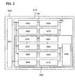
- Embodiment Mode 2 a structure and operation of a semiconductor device of the present invention when it is provided for an RFID tag will be described.
- the wireless communication system mainly includes a communication device 3010, an antenna unit 3020 which is electrically connected to the communication device 3010, an RFID tag 300, and a controlling terminal 3030 which controls the communication device.
- the RFID tag 300 includes an antenna 301 and a semiconductor IC 313. Note that the antenna 301 is not necessarily included in the RFID tag 300 of the present invention.
- the semiconductor IC 313 includes an input circuit 440, a circuit 450 which generates a constant voltage, a feedback circuit 460, a filter 470 and a circuit portion 360, which are components of the semiconductor device of the present invention.
- the circuit portion 360 includes a reset circuit 340, a demodulation circuit 350, a clock generation circuit 370, a code extraction circuit 380, a code determination circuit 390, a modulation circuit 400, a signal output controlling circuit 410, a CRC (cyclic redundancy check) circuit 420, and a memory 430.
- CRC cyclic redundancy check
- a radio signal is sent from the antenna unit 3020 which is electrically connected to the communication device 3010.
- the radio signal includes a command from the communication device 3010 to the RFID tag 300. Then, the radio signal is received by the antenna 301 included in the RFID tag 300.
- the radio signal received by the antenna 301 is sent as an AC signal, which is an electrical signal, to the input circuit 440.
- the input circuit 440 includes a rectifier circuit and a capacitor.
- the radio signal received is rectified by passing through the rectifier circuit and then smoothed by the capacitor. Then, a DC voltage (hereinafter also referred to as V IN ) is generated.
- a configuration of the input circuit 440 may be anything as long as the circuit can generate a DC voltage from a rectified signal.
- V IN is sent to the circuit 450 which generates a constant voltage, and the constant voltage (hereinafter also referred to as V DD ) is generated therein.
- V DD constant voltage
- V SS low power supply potential
- the generated constant voltage V DD is input to the feedback circuit 460 through the filter 470. Even when the feedback circuit 460 operates and the AC signal is transmitted, the transmitted AC signal is less likely to pass through the filter 470. Therefore, variation in the constant voltage V DD by the AC signal is suppressed.
- the radio signal received by the antenna 301 is also sent as the AC signal to the demodulation circuit 350.
- the demodulation circuit 350 rectifies and demodulates the signal.
- the demodulated signal may be amplified by providing an analog amplifier next to the demodulation circuit 350.
- a signal waveform becomes sharp. If the signal waveform has a gentle curve, delay of the signal is worsen and the operation becomes unstable. However, when the signal waveform has a sharp curve, delay of the signal is short and operation can be stable.
- the radio signal received by the antenna 301 is sent as the AC signal to the clock generation circuit 370.
- the clock generation circuit 370 divides the AC signal and generates a reference clock signal.
- the reference clock signal generated by the clock generation circuit 370 is sent to each circuit block and used for latch and selection of signals in each circuit block, time counting, and the like.
- the demodulated signal and the reference clock signal are sent to the code extraction circuit 380.
- the code extraction circuit 380 extracts a command, that is from the communication device 3010 to the RFID tag 300, from the demodulated signal.
- the code extraction circuit 380 generates a signal which controls the code determination circuit 390.
- the command extracted by the code extraction circuit 380 is sent to the code determination circuit 390.
- the code determination circuit 390 identifies the command from the communication device 3010.
- the code determination circuit 390 controls the CRC circuit 420, the memory 430, and the signal output controlling circuit 410.
- the command from the communication device 3010 is identified and the CRC circuit 420, the memory 430, and the signal output controlling circuit 410 are operated in accordance with the identified command. Then, a signal including unique data such as an ID number which is stored or written in the memory 430 is output, or data is stored in the memory 430.
- the signal output controlling circuit 410 converts the signal including unique data such as an ID number which is stored or written in the memory 430 into an encoded signal by an encoding method meeting a standard such as ISO.
- the radio signal received by the antenna 301 is modulated by the modulation circuit 400.
- the modulated signal is received by the antenna unit 3020 which is electrically connected to the communication device 3010. Then the received signal is analyzed in the communication device 3010 to recognize the unique data such as the ID number in the RFID tag 300 that uses the semiconductor device of the present invention.
- the semiconductor device of the present invention can suppress transmission of the AC signal. Accordingly, the constant voltage V DD is less likely to vary so that a malfunction or an operation defect such as complete inoperative can be prevented.
- This embodiment mode can be implemented by being combined as appropriate with any of the above-described embodiment modes.
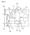
- Embodiment Mode 3 will describe a circuit configuration of a semiconductor device of the present invention.
- FIG 4 illustrates the circuit configuration.
- a semiconductor device 233 includes an input circuit 224, a circuit 225 which generates a constant voltage, a feedback circuit 226, a filter 227, and a circuit portion 228.
- Two input terminals + V and - V of the semiconductor device 233 are electrically connected to a + terminal and a - terminal, respectively, of an element, which receives a radio signal, such as an antenna.
- both a voltage applied to the + V terminal and a voltage applied to the - V terminal are AC voltages.
- a structure of the semiconductor device 233 will be specifically described with an example in which a voltage applied to the + V terminal is higher than that applied to the - V terminal.
- the input circuit 224 includes a first capacitor element 220, a first transistor 221, a second transistor 222, and a second capacitor element 223.
- One terminal of the first capacitor element 220 is connected to the + V terminal, and the other terminal is connected to a gate terminal and a source terminal of the first transistor 221.
- the gate terminal and the source terminal of the first transistor 221 are connected to each other and the first transistor 221 functions as a diode.
- a drain terminal of the first transistor 221 is connected to one terminal of the second capacitor element 223. Similar to the first transistor 221, a gate terminal and a source terminal of the second transistor 222 are connected to each other and the second transistor 222 functions as a diode.
- a drain terminal of the second transistor 222 is connected to the gate terminal and the source terminal of the first transistor 221. Furthermore, the gate terminal and the source terminal of the second transistor 222 are connected to the other terminal of the second capacitor element 223. Note that the other terminal of the second capacitor element 223 is also connected to the - V terminal.
- a half-wave voltage-doubling rectifier circuit is composed of the first capacitor element 220, the first transistor 221 and the second transistor 222.
- the filter 227 includes a first resistance element 230 and a third capacitor element 229.
- One terminal of the first resistance element 230 is connected to one terminal of the third capacitor element 229 and an output of the circuit 225 which generates a constant voltage; and the other terminal of the first resistance element 230 is connected to a gate terminal of a third transistor 231 included in the feedback circuit 226.
- the other terminal of the third capacitor element 229 is connected to the -V terminal.
- the third capacitor element 229 is connected to the - V terminal and one terminal of the first resistance element 230 in FIG 4 , the third capacitor element 229 can be connected to the -V terminal and the other terminal of the first resistance element 230.
- the feedback circuit 226 includes the third transistor 231 and a second resistance element 232.
- a source terminal of the third transistor 231 is connected to the - V terminal, the gate terminal is connected to the other terminal of the first resistance element 230 included in the filter 227, and a drain terminal is connected to one terminal of the second resistance element 232.
- the other terminal of the second resistance element 232 is connected to the other terminal of the first capacitor element 220 in the input circuit 224, and the gate terminal and the source terminal of the first transistor 221.
- FIG 4 illustrates an example of the feedback circuit 226 having the third transistor 231 and the second resistance element 232.
- the second resistance element 232 can be replaced with a capacitor element or a diode.
- the feedback circuit 226 may be any circuit as long as it changes impedance of the semiconductor device 233.
- a radio signal received by an antenna is input as an AC signal to the input circuit 224.
- the AC signal input to the input circuit 224 is rectified by the half-wave voltage-doubling rectifier circuit to generate a signal whose amplitude is approximately twice as large as the amplitude of a half-wave of the AC signal.
- the generated signal is smoothed in the second capacitor element 223 to be a DC voltage (hereinafter also referred to as V IN ) .
- the generated V IN is input to the circuit 225 which generates a constant voltage and a constant voltage (hereinafter also referred to as V DD ) whose voltage is lower and more constant than V IN is generated.
- V DD a constant voltage
- a circuit configuration may be anything as long as it can make the voltage constant which is generated by one or both of voltage and current. For example, a regulator circuit can be given.
- the generated V DD is supplied to the circuit portion 228. Note that the V DD passes through the filter 227 which is provided between the circuit 225 and the feedback circuit 226.
- the third transistor 231 becomes conductive (a transistor is turned on and current flows). Current flows from the other terminal of the first capacitor element 220 in the input circuit 224 to which the AC signal is input, from the gate terminal and the source terminal of the first transistor 221, and from the drain terminal of the second transistor 222 through the second resistance element 232 and the third transistor 231 whereby impedance of the semiconductor device 233 can be changed. However, transmission of the AC signal occurs at the same time.
- the V DD does not easily vary. Then, the V DD is supplied to the circuit portion 228.
- the frequency ( fc ), the capacitance value ( C ), and the resistance value ( R ) are expressed by a formula, f c ⁇ 1 / (2 ⁇ CR ).
- This formula shows that a frequency lower than 1 / (2 ⁇ CR ) is likely to pass through the filter while a frequency higher than 1 / (2 ⁇ CR ) is less likely to pass through the filter.
- This formula can estimate the capacitance value ( C ) and the resistance value ( R ) in accordance with the frequency of the AC signal whose transmission is to be suppressed.
- all transistors are N-type transistors but P-type transistors can also be used.
- a semiconductor device of the present invention can suppress transmission of an AC signal.
- the constant voltage is less likely to vary, so that a malfunction or an operation defect such as complete inoperative can be prevented.
- This embodiment mode can be implemented by being combined as appropriate with any of the aforementioned embodiment modes.
- Embodiment Mode 4 will describe another example of a filter circuit included in a semiconductor device of the present invention.
- FIG. 5 illustrates a circuit configuration.
- a semiconductor device 333 includes an input circuit 324, a circuit 325 which generates a constant voltage, a feedback circuit 326, a filter 327, and a circuit portion 328.
- Two input terminals + V and - V of the semiconductor device 333 are electrically connected to a + terminal and a - terminal, respectively, of an element, which receives a radio signal, such as an antenna.
- both a voltage applied to the + V terminal and a voltage applied to the - V terminal are AC voltages.
- a structure of the semiconductor device 333 will be specifically described with an example in which a voltage applied to the + V terminal is higher than that applied to the - V terminal.
- the input circuit 324 includes a first capacitor element 320, a first transistor 321, a second transistor 322, and a second capacitor element 323.
- One terminal of the first capacitor element 320 is connected to the + V terminal and the other terminal of the first capacitor element 320 is connected to a gate terminal and a source terminal of the first transistor 321.
- the gate terminal and the source terminal of the first transistor 321 are connected to each other, and the first transistor 321 functions as a diode.
- a drain terminal of the first transistor 321 is connected to one terminal of the second capacitor element 323.
- a gate terminal and a source terminal of the second transistor 322 are connected to each other like the first transistor 321, and the second transistor 322 functions as a diode.
- a drain terminal of the second transistor 322 is connected to the gate terminal and the source terminal of the first transistor 321. Furthermore, the gate terminal and the source terminal of the second transistor 322 are connected to the other terminal of the second capacitor element 323. Note that the other terminal of the second capacitor element 323 is also connected to the - V terminal.
- a half-wave voltage-doubling rectifier circuit is composed of the first capacitor element 320, the first transistor 321 and the second transistor 322.
- a filter 327 includes a first inductor element 330 and a third capacitor element 329.
- One terminal of the first inductor element 330 is connected to one terminal of the third capacitor element 329 and an output of the circuit 325 which generates a constant voltage.
- the other terminal of the first inductor element 330 is connected to a gate terminal of a third transistor 331 included in the feedback circuit 326.
- the other terminal of the third capacitor element 329 is connected to the - V terminal.
- the third capacitor element 329 may be connected to the -V terminal and the other terminal of the first inductor element 330.
- the feedback circuit 326 includes the third transistor 331 and a second resistance element 332.
- a source terminal, the gate terminal, and a drain terminal of the third transistor 331 are connected to the - V terminal, the other terminal of the first inductor element 330 included in the filter 327, and one terminal of the second resistance element 332, respectively.
- the other terminal of the second resistance element 332 is connected to the other terminal of the first capacitor element 320 in the input circuit 324, and the gate terminal and the source terminal of the first transistor 321.
- FIG. 5 illustrates an example of the feedback circuit 326 having the third transistor 331 and the second resistance element 332.
- the second resistance element 332 may be replaced with a capacitor element or a diode.
- the feedback circuit 326 may be any circuit as long as it changes impedance of the semiconductor device 333.
- a radio signal received by an antenna is input as an AC signal to the input circuit 324.
- the AC signal input to the input circuit 324 is rectified by the half-wave voltage-doubling rectifier circuit to generate a signal whose amplitude is approximately twice as large as the amplitude of a half-wave of the AC signal.
- the generated signal is smoothed in the second capacitor element 323 to be a DC voltage (hereinafter also referred to as V IN ).
- V IN is input to the circuit 325 which generates a constant voltage and a constant voltage (hereinafter referred to as V DD ) whose voltage is lower and more constant than V IN is generated.
- V DD a constant voltage
- a circuit configuration may be anything as long as it can make the voltage constant which is generated by one or both of voltage and current. For example, a regulator circuit can be given.
- the generated V DD is supplied to the circuit portion 328. Note that the V DD passes through the filter 327 which is provided between the circuit 325 and the feedback circuit 326.
- the third transistor 331 becomes conductive (a transistor is turned on and current flows). Current flows from the other terminal of the first capacitor element 320 in the input circuit 324 to which the AC signal is input, from the gate terminal and the source terminal of the first transistor 321, and from the drain terminal of the second transistor 322 through the second resistance element 332 and the third transistor 331 whereby impedance of the semiconductor device 333 can be changed. However, transmission of the AC signal occurs at the same time.
- the V DD does not easily vary. Then, the V DD is supplied to the circuit portion 328.
- the frequency ( fc ), the inductance ( L ), and the capacitance value ( C ) are expressed by a formula, fc ⁇ 1 / (2 ⁇ ( LC ) 1/2 ).
- This formula shows that a frequency lower than 1 / (2 ⁇ ( LC ) 1/2 ) is likely to pass through the filter while a frequency higher than 1 / (2 ⁇ ( LC ) 1/2 ) is less likely to pass through the filter.
- This formula can estimate the inductance ( L ) and the capacitance value ( C ) in accordance with frequency of the AC signal whose transmission is desired to be suppressed.
- all transistors are N-type transistors but P-type transistors can also be used.
- a semiconductor device of the present invention can suppress transmission of an AC signal.
- the constant voltage is less likely to vary, so that a malfunction or an operation defect such as complete inoperative can be prevented.
- This embodiment mode can be implemented by being combined as appropriate with any of the aforementioned embodiment modes.
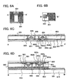
- Embodiment 1 manufacturing steps of a semiconductor device of the present invention will be described with reference to FIGS. 6A to 7D .
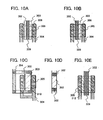
- FIGS. 6A to 6D illustrate a structural example of the antenna 301 in the RFID tag shown in FIG. 2 .
- the antenna 301 is provided in two ways, one of which (hereinafter referred to as a first antenna installation system) is shown in FIGS. 6A and 6C and the other (hereinafter referred to as a second antenna installation system) is shown in FIGS. 6B and 6D.
- FIG. 6C is a cross-sectional view along a line A-A' of FIG. 6A
- FIG. 6D is a cross-sectional view along a line B-B' of FIG 6B .
- the antenna 301 is provided over a substrate 600 over which a plurality of elements (hereinafter referred to as an element group 601) are provided (see FIGS. 6A and 6C ).
- a circuit other than the antenna in the semiconductor device of the present invention is formed of the element group 601.
- the element group 601 includes a plurality of thin film transistors.
- a conductive film functioning as the antenna 301 is provided in the same layer as a wire 666 which is connected to a source or drain of the thin film transistor included in the element group 601.
- the conductive film functioning as the antenna 301 may be provided in the same layer as a gate electrode 664 of the thin film transistor included in the element group 601, or may be provided over an insulating film which is provided so as to cover the element group 601.
- a terminal portion 602 is provided on the substrate 600 on which the element group 601 is provided. Then, the terminal portion 602 is connected to the antenna 301 which is formed over a substrate 610 which is different from the substrate 600 (see FIGS. 6B and 6D ).
- part of a wire 666 connected to a source or drain of the thin film transistor included in the element group 601 may be used as the terminal portion 602.
- the substrate 600 is attached to the substrate 610 over which the antenna 301 is provided, so that the antenna 301 is connected to the terminal portion 602.
- a conductive particle 603 and a resin 604 are provided between the substrate 600 and the substrate 610.
- the antenna 301 is electrically connected to the terminal portion 602 with the conductive particle 603.
- the substrate 600 for example, a glass substrate made of barium borosilicate glass, aluminoborosilicate glass, or the like, a quartz substrate, a ceramic substrate, or the like can be used. Alternatively, a semiconductor substrate of which the surface is provided with an insulating film may be used. A substrate made of a flexible synthetic resin such as plastic may also be used. The surface of the substrate may be planarized by polishing using a CMP method or the like. A substrate which is thinned by polishing a glass substrate, a quartz substrate, or a semiconductor substrate may be used as well.
- a base film 661 formed on the substrate 600 an insulating film made of silicon oxide, silicon nitride, silicon nitride oxide, or the like can be used.
- the base film 661 can prevent an alkali metal such as Na or an alkaline earth metal contained in the substrate 600, from being diffused in a semiconductor layer 662 and adversely affecting characteristics of the thin film transistor.
- the base film 661 shown in FIGS. 6C and 6D has a single-layer structure, it may have a two or more layer structure. Note that when the diffusion of impurities is not a serious problem such as in a quartz substrate, the base film 661 is not necessarily provided.
- the surface of the substrate 600 may be directly processed by high density plasma to form the base film 661.
- the high density plasma is generated using a microwave, for example, in 2.45 GHz.
- High density plasma with an electron density of 10 11 to 10 13 /cm 3 , an electron temperature of 2 eV or lower, and an ion energy of 5 eV or lower is used. Since such high density plasma featuring a low electron temperature has low kinetic energy of active species, a film with less plasma damage and defects can be formed compared to that formed by conventional plasma treatment.
- Plasma can be generated using a plasma processing apparatus utilizing microwave excitation, which employs a radial slot antenna. The distance between the antenna which generates a microwave and the substrate 600 is set at 20 to 80 mm (preferably, 20 to 60 mm).
- the surface of the substrate 600 can be nitrided by performing the high density plasma treatment in a nitrogen atmosphere, for example an atmosphere containing nitrogen (N) and a rare gas (containing at least one of He (helium), Ne (neon), Ar (argon), Kr (krypton), and Xe (xenon)), an atmosphere containing nitrogen, hydrogen (H), and a rare gas, or an atmosphere containing ammonium (NH 3 ) and a rare gas.
- a nitride layer formed on the surface of the substrate 600 contains silicon nitride as a main component.
- the nitride layer can be used as a blocking layer against impurities diffused from the substrate 600 side.
- a silicon oxide film or a silicon oxynitride film may be formed on the nitride layer by a plasma CVD method and may be used as the base film 661.
- the surface of the base film 661 made of silicon oxide, silicon oxynitride, or the like When similar high density plasma treatment is applied to the surface of the base film 661 made of silicon oxide, silicon oxynitride, or the like, the surface and a region with a depth of 1 to 10 nm from the surface can be nitrided.
- This extremely thin silicon nitride layer is favorable since it functions as a blocking layer and has less stress on the semiconductor layer 662 formed on this extremely thin silicon nitride layer.
- a crystalline semiconductor film or an amorphous semiconductor film, which is patterned into a desired shape can be used.
- an organic semiconductor film may be used.
- a crystalline semiconductor film can be obtained by crystallizing an amorphous semiconductor film.
- a laser crystallization method, a thermal crystallization method using RTA or an annealing furnace, a thermal crystallization method using a metal element which promotes crystallization, or the like can be used as the crystallization method.
- the semiconductor layer 662 includes a channel formation region 662a and a pair of impurity regions 662b to which an impurity element imparting a conductivity type is added.
- low concentration impurity regions 662c to which the impurity element is added at a lower concentration than that of the impurity regions 662b are provided between the channel formation region 662a and the pair of impurity regions 662b, the present invention is not limited to this.
- the low concentration impurity regions 662c are not necessarily provided.
- An impurity element which imparts a conductivity type may be added to the channel formation region 662a of the thin film transistor. In this manner, the threshold voltage of the thin film transistor can be controlled.
- a first insulating layer 663 can have a single-layer or a stack of a plurality of films made of silicon oxide, silicon nitride, silicon nitride oxide, or the like.
- the surface of the first insulating layer 663 may be processed by high density plasma in an oxygen atmosphere or a nitrogen atmosphere, thereby being oxidized or nitrided to be densified.
- the high density plasma is generated using a microwave, for example, in 2.45 GHz, as described above. Note that high density plasma with an electron density of 10 11 to 10 13 /cm 3 , an electron temperature of 2 eV or lower, and an ion energy of 5 eV or lower is used.
- Plasma can be generated using a plasma processing apparatus utilizing microwave excitation, which employs a radial slot antenna.
- the distance between the antenna which generates a microwave and the substrate 600 is set at 20 to 80 mm (preferably, 20 to 60 mm).
- the high density plasma treatment may be applied to the surface of the semiconductor layer 662 so that the surface of the semiconductor layer is oxidized or nitrided.
- the treatment in an oxygen atmosphere or a nitrogen atmosphere with the substrate 600 at a temperature of 300 to 450 °C, a favorable interface with the first insulating layer 663 which is formed on the semiconductor layer 662 can be obtained.
- an atmosphere containing nitrogen (N) and a rare gas containing at least one of He (helium), Ne (neon), Ar (argon), Kr (krypton), and Xe (xenon)
- an atmosphere containing nitrogen, hydrogen (H), and a rare gas or an atmosphere containing ammonium (NH 3 ) and a rare gas
- an atmosphere containing oxygen (O) and a rare gas an atmosphere containing oxygen, hydrogen (H), and a rare gas, or an atmosphere containing dinitrogen monoxide (N 2 O) and a rare gas can be used.
- the gate electrode 664 may have a single-layer structure or stacked-layer structure including one element selected from Ta (tantalum), W (tungsten), Ti (titanium), Mo (molybdenum), Al (aluminum), Cu (copper), Cr (chromium), or Nd (neodymium), or an alloy or a compound containing a plurality of the above-described elements.
- the gate electrode 664 has a two-layer structure.
- a thin film transistor is formed of the semiconductor layer 662, the gate electrode 664, and the first insulating layer 663 functioning as a gate insulating film between the semiconductor layer 662 and the gate electrode 664.
- the thin film transistor has a top gate structure; however, it may be a bottom gate transistor having a gate electrode under the semiconductor layer, or a dual gate transistor having gate electrodes over and under the semiconductor layer.
- a second insulating layer 667 is desirably an insulating film such as a silicon nitride film, which has barrier properties to block ion impurities.
- the second insulating layer 667 is made of silicon nitride or silicon oxynitride.
- the second insulating layer 667 functions as a protective film to prevent contamination of the semiconductor layer 662.
- hydrogen gas may be introduced and the aforementioned high density plasma treatment may be applied, thereby hydrogenating the second insulating layer 667.
- the second insulating layer 667 may be nitrided and hydrogenated by introducing ammonium (NH 3 ) gas.
- oxidization-nitridation treatment and hydrogenation treatment may be performed by introducing oxygen, dinitrogen monoxide (N 2 O) gas, and the like together with hydrogen gas.
- N 2 O dinitrogen monoxide
- oxidization treatment, or oxidization-nitridation treatment in this manner, the surface of the second insulating layer 667 can be densified. As a result, the function of the second insulating layer 667 as a protective film can be enhanced.
- Hydrogen introduced into the second insulating layer 667 is discharged when thermal treatment is applied at a temperature of 400 to 450 °C, thereby hydrogenating the semiconductor layer 662.
- the hydrogenation treatment may be performed in combination with hydrogenation treatment using the first insulating layer 663.
- a third insulating layer 665 can have a single-layer structure or a stacked-layer structure of an inorganic insulating film or an organic insulating film.
- an inorganic insulating film a silicon oxide film formed by a CVD method, a silicon oxide film formed by an SOG (spin on glass) method, or the like can be used.
- an SOG (spin on glass) method or the like can be used.
- an organic insulating film a film made of polyimide, polyamide, BCB (benzocyclobutene), acrylic, a positive photosensitive organic resin, a negative photosensitive organic resin, or the like can be used.
- the third insulating layer 665 may be made of a material having a skeleton structure formed of a bond of silicon (Si) and oxygen (O).
- An organic group containing at least hydrogen (such as an alkyl group and aromatic hydrocarbon) is used as a substituent of this material.
- a fluoro group may be used as the substituent.
- a fluoro group and an organic group containing at least hydrogen may be used as the substituent.
- the wire 666 can have a single-layer structure or a stacked-layer structure including one element selected from Al (aluminum), Ni (nickel), W (tungsten), Mo (molybdenum), Ti (titanium), Pt (platinum), Cu (copper), Ta (tantalum), Au (gold), or Mn (manganese), or an alloy containing a plurality of the above-described elements.
- a single-layer structure is shown as an example.
- the wire 666 functions as a wire connected to the source or drain of the thin film transistor and also as the antenna 301.
- the wire 666 functions as the wire connected to the source or drain of the thin film transistor and also as the terminal portion 602.
- the antenna 301 can also be formed by a droplet discharge method using a conductive paste containing nano-particles such as Au, Ag, and Cu.
- the droplet discharge method is a collective term for a method for forming a pattern by discharging droplets, such as an ink jet method and a dispenser method, which has advantages in that the utilization efficiency of a material is improved, and the like.
- a fourth insulating layer 668 is formed over the wire 666.
- the fourth insulating layer 668 can have a single-layer structure or a stacked-layer structure of an inorganic insulating film or an organic insulating film.
- the fourth insulating layer 668 functions as a protective layer of the antenna 301.
- the element group 601 may use the one formed over the substrate 600 (see FIG. 7A ) as it is, the element group 601 over the substrate 600 may be separated (see FIG. 7B ), and the element group 601 may be attached to a flexible substrate 701 (see FIG. 7C ).
- the flexible substrate 701 has flexibility, and for example, a plastic substrate such as polycarbonate, polyarylate, and polyethersulfone, a ceramic substrate, or the like can be used.
- any of the following can be used: (A) a method in which a release layer is provided in advance between the substrate 600 and the element group 601 and the release layer is removed by an etchant; (B) a method in which the release layer is partially removed by an etchant, and then the substrate 600 and the element group 601 are separated physically; and (C) a method in which the substrate 600 with high heat resistance over which the element group 601 is formed is eliminated mechanically or removed by etching with a solution or gas so that the element group 601 is separated.
- “to be separated by a physical means” denotes that to be separated by applying stress from outside, for example, to be separated by applying stress from a wind pressure of gas sprayed from a nozzle, an ultrasonic wave, or the like.
- a method in which a metal oxide film is provided between the substrate 600 with high heat resistance and the element group 601, and the metal oxide film is weakened by crystallization to separate the element group 601 can be used; or a method in which an amorphous silicon film containing hydrogen is provided between the substrate 600 with high heat resistance and the element group 601, and the amorphous silicon film is removed by irradiation with a laser beam or etching so that the element group 601 is separated can be used.
- a commercial adhesive may be used, and for example, an adhesive such as an epoxy resin-based adhesive or a resin additive may be used.
- a thin and light semiconductor device which is not easily broken even when fallen to the ground is obtained (see FIG. 7C ).
- an inexpensive flexible substrate 701 an inexpensive semiconductor device can be provided.
- the flexible substrate 701 having flexibility can be attached to a curved surface or an irregular-shaped substance, which realizes various kinds of usage.
- a wireless tag 720 as one mode of a semiconductor device of the present invention can be attached to a curved surface such as a medicine bottle (see FIG. 7D ).
- a semiconductor device can be manufactured at low cost.
- this embodiment describes a thin film transistor as an example, the present invention is not limited thereto.
- a transistor formed of a single crystalline silicon, a transistor formed of SOI, or the like can be used.
- a transistor formed of an organic semiconductor or a transistor formed of a carbon nanotube can be used.
- a semiconductor device includes a flexible protective layer 801, a flexible protective layer 803 including an antenna 802, and an element group 804 formed by a separation process or thinning of a substrate.
- the element group 804 can have a similar structure to the element group 601 described in the Embodiment 1.
- the antenna 802 formed over the protective layer 803 is electrically connected to the element group 804.
- the antenna 802 is formed only over the protective layer 803; however, the present invention is not limited to this structure and the antenna 802 may be formed over the protective layer 801 as well.
- a barrier film made of a silicon nitride film or the like may be formed between the element group 804 and each of the protective layer 801 and the protective layer 803. As a result, contamination of the element group 804 can be prevented, which leads to a semiconductor device with improved reliability.
- the antenna 802 can be formed of Ag, Cu, or a metal plated with Ag or Cu.
- the element group 804 and the antenna 802 can be connected to each other using an anisotropic conductive film and applying ultraviolet treatment or ultrasonic wave treatment. Note that the element group 804 and the antenna 802 may be attached to each other using a conductive paste or the like.
- FIG. 8B shows a cross-sectional structure of the thus formed semiconductor device.
- a thickness of the element group 804 which is sandwiched is 5 ⁇ m or less ( ⁇ 5 ⁇ m), and preferably 0.1 to 3 ⁇ m.
- each of the protective layer 801 and the protective layer 803 which overlap each other have a thickness of d
- each of the protective layer 801 and the protective layer 803 preferably has a thickness of ( d /2) ⁇ 30 ⁇ m, and more preferably ( d /2) ⁇ 10 ⁇ m.
- each of the protective layer 801 and the protective layer 803 desirably has a thickness of 10 to 200 ⁇ m.
- the element group 804 has an area of 10 mm square (100 mm 2 ) or smaller, and desirably 0.3 to 4 mm square (0.09 to 16 mm 2 ).
- Each of the protective layer 801 and the protective layer 803 is made of an organic resin material, and thus has high resistance against bending.
- the element group 804 which is formed by a separation process or thinning of a substrate also has higher resistance against bending compared to a single crystal semiconductor. Since the element group 804, the protective layer 801, and the protective layer 803 can be tightly attached to each other without any space, a completed semiconductor device itself also has high resistance against bending.
- the element group 804 surrounded by the protective layer 801 and the protective layer 803 may be provided over a surface or inside of another object, or embedded in paper.
- FIG 8C shows one transistor 881 selected from the element group 804.
- a current flows from one 805 of a source and a drain to the other 806 of the source and the drain in response to a potential of a gate electrode 807.
- the transistor 881 is provided so that a direction of the current flow in the transistor 881 (carrier movement direction) and the direction of the arc of a substrate 880 cross at right angles. With such an arrangement, the transistor 881 is less affected by stress even when the substrate 880 is bent to be an arc, and thus variations in characteristics of the transistor 881 included in the element group 804 can be suppressed.
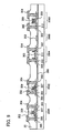
- FIG. 9 shows a cross-sectional structure of such transistors included in a circuit.
- FIG. 9 shows an N-channel transistor 2001, an N-channel transistor 2002, a capacitor element 2004, a resistor element 2005, and a P-channel transistor 2003.
- Each of the transistors includes a semiconductor layer 305, an insulating layer 308, and a gate electrode 309.
- the gate electrode 309 has a stacked-layer structure of a first conductive layer 303 and a second conductive layer 302.
- FIGS. 10A to 10E are top views corresponding to the transistor, the capacitor element, and the resistance element shown in FIG. 9.
- FIG. 9 and FIGS. 10A to 10E can be referred by corresponding with each other.
- FIG. 9 shows that, in the N-channel transistor 2001, impurity regions 307, which are also referred to as a lightly doped drain (LDD) regions, are formed in the semiconductor layer 305 on both sides of a channel region in a channel length direction (a direction of carrier flow).
- the impurity regions 307 are doped at a lower concentration than the impurity concentration of impurity regions 306 that form a source region and a drain region which are in contact with wires 304.
- the impurity regions 306 and the impurity regions 307 are added with an impurity imparting N-type conductivity, such as phosphorus.
- the LDD regions are formed to suppress hot electron degradation and short channel effects.
- the first conductive layer 303 is extensively provided on both sides of the second conductive layer 302.
- the thickness of the first conductive layer 303 is smaller than that of the second conductive layer 302.
- the first conductive layer 303 is formed to have such a thickness that ion species accelerated with an electric field of 10 to 100 kV can pass through the first conductive layer 303.
- the impurity regions 307 are formed so as to overlap with the first conductive layer 303 of the gate electrode 309. In other words, the LDD regions overlapping with the gate electrode 309 are formed.
- the impurity regions 307 are formed in a self-alignment manner by addition of an impurity having one conductivity type through the first conductive layer 303 using the second conductive layer 302 as a mask. That is, the LDD regions overlapping with the gate electrode are formed in a self-alignment manner.
- a transistor having LDD regions on both sides of a channel region is applied to a transistor constituting a transmission gate (also referred to as an analog switch) used for a logic circuit, or rectifier transistors such as the first transistor 221 and the second transistor 222 which configure a half-wave voltage-doubling rectifier circuit in the input circuit 224 shown in FIG. 4 .
- a transistor preferably includes LDD regions on both sides of the channel region, since positive and negative voltages are applied to source and drain electrodes.
- the impurity region 307 doped with an impurity element at a lower concentration than impurity concentration of the impurity regions 306 is formed on one side of the gate electrode in the semiconductor layer 305.
- the first conductive layer 303 is provided extensively on one side of the second conductive layer 302.
- the LDD region can be formed in a self-alignment manner by addition of an impurity having one conductivity type through the first conductive layer 303 using the second conductive layer 302 as a mask.
- a transistor having an LDD region on one side may be applied to a transistor in which only one of a positive voltage and a negative voltage is applied between a source electrode and a drain electrode.
- the transistor having an LDD region on one side may be applied to a transistor constituting a logic gate such as an inverter circuit, a NAND circuit, a NOR circuit, and a latch circuit, or a transistor generating an analog circuit such as a sense amplifier, the circuit 225 which generates a constant voltage in FIG. 4 , and a VCO (voltage controlled oscillator).
- the capacitor element 2004 has a structure in which the insulating layer 308 is sandwiched between the first conductive layer 303 and the semiconductor layer 305.
- the semiconductor layer 305 of the capacitor element 2004 includes impurity regions 310 and an impurity region 311.
- the impurity region 311 is formed in the semiconductor layer 305 so as to overlap with the first conductive layer 303.
- the impurity regions 310 are in contact with the wires 304. Since an impurity having one conductivity type can be added to the impurity region 311 through the first conductive layer 303, the impurity regions 310 and the impurity region 311 may have the same concentration or different concentrations of an impurity.
- the semiconductor layer 305 of the capacitor element 2004 functions as an electrode; therefore, it is preferable that an impurity having one conductivity type be added to the semiconductor layer 305 to reduce the resistance thereof.
- the first conductive layer 303 can effectively function as an electrode by utilizing the second conductive layer 302 as an auxiliary electrode as shown in FIG. 10C .
- Such a composite electrode structure combining the first conductive layer 303 and the second conductive layer 302 allows the capacitor element 2004 to be formed in a self-alignment manner.
- the capacitor element 2004 can be used as the first capacitor element 220 and the second capacitor element 223 included in the input circuit 224, and the third capacitor element 229 included in the filter 227, which are shown in FIG. 4 , or a resonant capacitor included in the antenna 301 shown in FIG. 2 .
- the resonant capacitor is required to function as a capacitor regardless of a positive or negative voltage applied between two terminals of the capacitor element, since both positive and negative voltages are applied between the two terminals.
- the resonant capacitor constitutes the antenna 301 and a resonant circuit to resonate with the frequency of a radio signal sent from an antenna connected to a reader/writer.
- the resistor element 2005 includes the first conductive layer 303.
- the first conductive layer 303 is formed to have a thickness of approximately 30 to 150 nm; therefore, the resistor element can be formed by setting the width and length thereof as appropriate.
- the resistor element can be used as the resistance element 230 included in the filter 227, as well as the second resistance element 232 included in the feedback circuit 226, which are shown in FIG. 4 .
- the resistance element is, in some cases, also used as a load when current is controlled by a VCO or the like.
- the resistor element may be formed using a semiconductor layer containing an impurity at a high concentration, or a thin metal layer. The resistance of a semiconductor layer depends on the film thickness, film quality, impurity concentration, activation rate, and the like whereas the resistance of a metal layer is determined by the film thickness and film quality and has few variations, which is preferable.
- the semiconductor layer 305 includes impurity regions 312 in the P-channel transistor 2003.
- the impurity regions 312 function as source and drain regions which are in contact with the wires 304 through an interlayer insulating film 20.
- the gate electrode 309 has a structure in which the first conductive layer 303 and the second conductive layer 302 overlap with each other (see FIG. 9 and 10E ).
- the P-channel transistor 2003 is a transistor with a single drain structure in which an LDD region is not provided.
- an impurity which imparts P-type conductivity, such as boron is added to the impurity regions 312.
- an N-channel transistor with a single drain structure can be obtained.
- One or both of the semiconductor layer 305 and the insulating layer 308 may be oxidized or nitrided by high density plasma treatment. This treatment can be performed in a similar manner to that described in Embodiment 1.
- the defect level at the interface between the semiconductor layer 305 and the insulating layer 308 can be reduced.
- this treatment is applied to the insulating layer 308, the insulating layer 308 can be densified. In other words, generation of defective charges and variations in the threshold voltage of the transistor can be suppressed.
- an insulating layer which is oxidized or nitrided by the plasma treatment can be used as the insulating layer 308.
- the insulating layer 308 can be formed by combining an insulating layer formed over the surface of the semiconductor layer 305 by the plasma treatment and an insulating layer deposited by a CVD method (a plasma CVD method or a thermal CVD method).
- the insulating layer may be used as a dielectric layer of the capacitor element 2004.
- the insulating layer formed by the plasma treatment is a dense film with a thickness of 1 to 10 nm; therefore, the capacitor element 2004 with large charge capacity can be obtained.
- the elements with various structures can be formed by combining conductive layers with different thicknesses.
- a region where only the first conductive layer is formed and a region where the first conductive layer and the second conductive layer are stacked can be formed using a photomask or a reticle provided with a diffraction grating pattern or an auxiliary pattern having an optical intensity reducing function formed of a semitransparent film. That is, in a photolithography process, the quantity of transmitted light through the photomask is controlled in exposing the photoresist to light so that the thickness of a resist mask to be developed is changed.
- a slit at the resolution limit or less may be provided in the photomask or the reticle to form the above-described resist having the different thickness.
- a mask pattern made from a photoresist material can be changed in shape.
- the region where only the first conductive layer is formed and the region where the first conductive layer and the second conductive layer are stacked can be formed in succession.
- the region where only the first conductive layer is formed can be formed as selected over the semiconductor layer.
- Such a region is effective over the semiconductor layer, but is not required in the other region (a wire region which is connected to the gate electrode). Since the region where only the first conductive layer is formed is not required to be formed in the wire portion by using this photomask or reticle, wire density can be highly improved.
- the first conductive layer is formed to have a thickness of 30 to 50 nm using a high melting point metal such as tungsten (W), chromium (Cr), tantalum (Ta), tantalum nitride, or molybdenum (Mo), or an alloy or a compound containing a high melting point metal as its main component.
- a high melting point metal such as tungsten (W), chromium (Cr), tantalum (Ta), tantalum nitride, or molybdenum (Mo)
- Mo molybdenum
- the first conductive layer and the second conductive layer are made of different conductive materials so as to have a difference in etching rate in the subsequent etching step.
- the first conductive layer and the second conductive layer may be made of, for example, tantalum nitride and a tungsten film, respectively.
- transistors having different electrode structures, a capacitor element, and a resistance element can be formed separately with the same patterning process by using the photomask or the reticle which is provided with a diffraction grating pattern or an auxiliary pattern having an optical intensity reducing function formed of a semitransparent film. Accordingly, in accordance with circuit characteristics, elements having different modes can be formed without increasing the number of steps, and integrated.
- the RFID tag 300 can be incorporated in, for example, bills, coins, securities, bearer bonds, certificates (driving license, resident card, and the like, see FIG 12A ), containers for wrapping objects (wrapping paper, bottle, and the like, see FIG 12B ), recording media such as DVD software, CDs, and video tapes (see FIG. 12C ), vehicles such as cars, motorbikes, and bicycles (see FIG 12D ), personal belongings such as bags and glasses (see FIG 12E ), foods, clothes, commodities, electronic apparatuses, and the like.
- the electronic apparatuses include a liquid crystal display device, an EL display device, a television set (also simply referred to as a television or a television receiver), a mobile phone, and the like.
- the RFID tag 300 can be fixed to an object by being attached to the surface of the object or embedded in the object.
- the RFID tag 300 may be embedded in paper of a book, or organic resin of a package.
- the RFID tag 300 is incorporated in bills, coins, securities, bearer bonds, certificates, and the like, forgery thereof can be prevented.
- RFID tag 300 is incorporated in containers for wrapping objects, recording media, personal belongings, foods, clothes, commodities, electronic apparatuses, and the like, an inspection system, a rental system of a rental shop, and the like can be performed more efficiently.
- the RFID tag 300 can also prevent vehicles from being forged or stolen.
- the RFID tag 300 is implanted into creatures such as animals, each creature can be identified easily.
- the wireless tag is implanted into creatures such as domestic animals, the year of birth, sex, breed, and the like thereof can be identified easily.
- the semiconductor device 201 of the present invention can be incorporated in any object (including creatures).
- the semiconductor device 201 has various advantages such that data can be sent and received through wireless communication, the semiconductor device 201 can be processed into various shapes, and wide directivity and recognition range are achieved depending on a selected frequency.
- a reader/writer 820 is provided on a side of a portable terminal including a display portion 821 and the RFID tag 300 including the semiconductor device 201 is provided on a side of an object 822 (see FIG. 11A ).
- the reader/writer 820 is brought close to the RFID tag 300 including the semiconductor device 201 included in the object 822, information on the object 822, such as ingredients, place of origin, test result in each production step, history of the distribution process, and explanation of the object is displayed on the display portion 821.
- the object 826 can be inspected by using the reader/writer 824 and the RFID tag 300 including the semiconductor device 201 when the object 826 is transported by a conveyor belt (see FIG 11B ).
- the semiconductor device 201 of the present invention for a system, information can be easily obtained and a system with high performance and high added value can be provided.
Landscapes
- Engineering & Computer Science (AREA)
- Computer Hardware Design (AREA)
- Microelectronics & Electronic Packaging (AREA)
- Physics & Mathematics (AREA)
- General Physics & Mathematics (AREA)
- Theoretical Computer Science (AREA)
- Computer Networks & Wireless Communication (AREA)
- Semiconductor Integrated Circuits (AREA)
- Near-Field Transmission Systems (AREA)
Claims (6)
- Halbleitervorrichtung, die umfasst:eine Eingangsschaltung (204, 440, 224, 324), die eine Gleichspannung aus einem Wechselstromsignal erzeugt;eine Schaltung (205, 450, 225, 325), die eine konstante Spannung unter Verwendung der Gleichspannung erzeugt;einen Schaltungsteil (208, 360, 228, 328), der mit der konstanten Spannung aus der Schaltung (205, 450, 225, 325) versorgt wird;ein Filter (207, 470, 227, 327); undeine Rückkopplungsschaltung (206, 460, 226, 326), die einen Anschluss umfasst, der elektrisch mit einem Eingang der Eingangsschaltung (204, 440, 224, 324) verbunden ist, wobei die Rückkopplungsschaltung ferner einen Transistor (231, 331) umfasst,wobei das Filter (207, 470, 227, 327) zwischen einem Ausgang der Schaltung (205, 450, 225, 325), die konfiguriert ist, um eine konstante Spannung zu erzeugen, und einem Gate des Transistors (231, 331) in der Rückkopplungsschaltung (206, 460, 226, 326) eingesetzt ist, undwobei die Rückkopplungsschaltung (206, 460, 226, 326) konfiguriert ist, um ihre Impedanz entsprechend der konstanten Spannung zu verändern, die durch das Filter (207, 470, 227, 327) in das Gate des Transistors (231, 331) eingegeben wird.
- Halbleitervorrichtung nach Anspruch 1,
wobei das Filter (227) ein erstes Widerstandelement (230) und ein Kondensatorelement (229) aufweist,
wobei die Rückkopplungsschaltung (226) ein zweites Widerstandelement (232) aufweist,
wobei der Ausgang der Schaltung (225), die die konstante Spannung erzeugt, mit einem Anschluss des ersten Widerstandelements (230), einem Anschluss des Kondensatorelements (229) und einem Eingang des Schaltungsteils (228) verbunden ist,
wobei der andere Anschluss des ersten Widerstandelements (230) mit dem Gate des Transistors (231) verbunden ist, und
wobei einer von Source und Drain des Transistors (231) mit einem Anschluss des zweiten Widerstandelements (232) verbunden ist. - Halbleitervorrichtung nach Anspruch 1,
wobei das Filter (327) ein Induktionselement (330) und ein Kondensatorelement (329) aufweist,
wobei die Rückkopplungsschaltung (326) ein Widerstandelement (332) aufweist,
wobei der Ausgang der Schaltung (325), die die konstante Spannung erzeugt, mit einem Anschluss des Induktionselements (330), einem Anschluss des Kondensatorelements (329) und einem Eingang des Schaltungsteils (328) verbunden ist,
wobei der andere Anschluss des Induktionselements (330) mit dem Gate des Transistors (331) verbunden ist, und
wobei einer von Source und Drain des Transistors (331) mit einem Anschluss des Widerstandelements (332) verbunden ist. - Halbleitervorrichtung nach Anspruch 1, die ferner umfasst:eine Antenne, wobei die Antenne zur Datenkommunikation durch drahtlose Kommunikation fähig ist;wobei das Wechselstromsignal aus der Antenne zu der Eingangsschaltung gesendet wird.
- Halbleitervorrichtung nach Anspruch 4,
wobei das Filter (227) ein erstes Widerstandelement (230) und ein Kondensatorelement (229) aufweist,
wobei die Rückkopplungsschaltung (226) ein zweites Widerstandelement (232) aufweist,
wobei der Ausgang der Schaltung (225), die die konstante Spannung erzeugt, mit einem Anschluss des ersten Widerstandelements (230), einem Anschluss des Kondensatorelements (229) und einem Eingang des Schaltungsteils (228) verbunden ist,
wobei der andere Anschluss des ersten Widerstandelements (230) mit dem Gate des Transistors (231) verbunden ist,
wobei einer von Source und Drain des Transistors (231) mit einem Anschluss des zweiten Widerstandelements (232) verbunden ist, und
wobei der andere von Source und Drain des Transistors (231) mit einem Anschluss der Antenne und dem anderen Anschluss des Kondensatorelements (229) verbunden ist. - Halbleitervorrichtung nach Anspruch 4,
wobei das Filter (327) ein Induktionselement (330) und ein Kondensatorelement (329) aufweist,
wobei die Rückkopplungsschaltung (326) ein Widerstandelement (332) aufweist,
wobei der Ausgang der Schaltung (325), die die konstante Spannung erzeugt, mit einem Anschluss des Induktionselements (330), einem Anschluss des Kondensatorelements (329) und einem Eingang des Schaltungsteils (328) verbunden ist,
wobei der andere Anschluss des Induktionselements (330) mit dem Gate des Transistors (331) verbunden ist,
wobei einer von Source und Drain des Transistors (331) mit einem Anschluss des Widerstandelements (332) verbunden ist, und
wobei der andere von Source und Drain des Transistors (332) mit einem Anschluss der Antenne und dem anderen Anschluss des Kondensatorelements (329) verbunden ist.
Applications Claiming Priority (1)
| Application Number | Priority Date | Filing Date | Title |
|---|---|---|---|
| JP2007074085 | 2007-03-22 |
Publications (2)
| Publication Number | Publication Date |
|---|---|
| EP1973069A1 EP1973069A1 (de) | 2008-09-24 |
| EP1973069B1 true EP1973069B1 (de) | 2013-01-02 |
Family
ID=39531426
Family Applications (1)
| Application Number | Title | Priority Date | Filing Date |
|---|---|---|---|
| EP08004115A Not-in-force EP1973069B1 (de) | 2007-03-22 | 2008-03-05 | Halbleiterbauelement |
Country Status (3)
| Country | Link |
|---|---|
| US (1) | US8331873B2 (de) |
| EP (1) | EP1973069B1 (de) |
| JP (1) | JP5144313B2 (de) |
Families Citing this family (6)
| Publication number | Priority date | Publication date | Assignee | Title |
|---|---|---|---|---|
| WO2010032573A1 (en) * | 2008-09-17 | 2010-03-25 | Semiconductor Energy Laboratory Co., Ltd. | Semiconductor device |
| KR101681884B1 (ko) * | 2009-03-27 | 2016-12-05 | 가부시키가이샤 한도오따이 에네루기 켄큐쇼 | 반도체장치, 표시장치 및 전자기기 |
| US8928466B2 (en) * | 2010-08-04 | 2015-01-06 | Semiconductor Energy Laboratory Co., Ltd. | Semiconductor device |
| KR102013402B1 (ko) | 2012-08-13 | 2019-08-22 | 삼성전자주식회사 | Rfid 장치 |
| JP6669132B2 (ja) * | 2017-06-23 | 2020-03-18 | 株式会社村田製作所 | マルチプレクサ、送信装置および受信装置 |
| US11886216B2 (en) * | 2021-11-02 | 2024-01-30 | Nxp B.V. | Voltage regulator circuit and method for regulating a voltage |
Family Cites Families (21)
| Publication number | Priority date | Publication date | Assignee | Title |
|---|---|---|---|---|
| JPH08186513A (ja) * | 1994-12-27 | 1996-07-16 | Toshiba Corp | 無線カード通信装置 |
| US5804997A (en) * | 1995-09-19 | 1998-09-08 | Fujitsu Limited | Current-to-voltage converting device and light receiver |
| JPH10260741A (ja) * | 1997-03-17 | 1998-09-29 | Oki Electric Ind Co Ltd | 定電圧発生回路 |
| JP3940939B2 (ja) | 1997-09-08 | 2007-07-04 | 吉川アールエフシステム株式会社 | データキャリア |
| JP3892563B2 (ja) | 1998-01-22 | 2007-03-14 | 株式会社東芝 | 情報記憶媒体 |
| US6134130A (en) * | 1999-07-19 | 2000-10-17 | Motorola, Inc. | Power reception circuits for a device receiving an AC power signal |
| AU2000260170A1 (en) * | 2000-07-14 | 2002-01-30 | Yamatake Corporation | Electromagnetically coupled device |
| US6509727B2 (en) * | 2000-11-24 | 2003-01-21 | Texas Instruments Incorporated | Linear regulator enhancement technique |
| JP2002368647A (ja) | 2001-06-06 | 2002-12-20 | Matsushita Electric Ind Co Ltd | データキャリア |
| US6954053B2 (en) * | 2002-07-10 | 2005-10-11 | Atmel Corporation | Interface for shunt voltage regulator in a contactless smartcard |
| JP3614157B2 (ja) * | 2002-07-30 | 2005-01-26 | オムロン株式会社 | Rfidタグならびにrfidタグにおける共振周波数の調整方法 |
| JP4380275B2 (ja) | 2003-09-12 | 2009-12-09 | ソニー株式会社 | データ通信装置 |
| US7026824B2 (en) * | 2003-10-31 | 2006-04-11 | Faraday Technology Corp. | Voltage reference generator with negative feedback |
| JP2005234827A (ja) | 2004-02-18 | 2005-09-02 | Sony Corp | アンテナモジュール及びこれを備えた携帯情報端末 |
| JP4096315B2 (ja) * | 2004-08-04 | 2008-06-04 | セイコーエプソン株式会社 | 表示システム |
| KR100554889B1 (ko) | 2005-03-21 | 2006-03-03 | 주식회사 한림포스텍 | 무접점 충전 시스템 |
| US20060267769A1 (en) * | 2005-05-30 | 2006-11-30 | Semiconductor Energy Laboratory Co., Ltd. | Terminal device and communication system |
| WO2006137573A1 (en) * | 2005-06-24 | 2006-12-28 | Semiconductor Energy Laboratory Co., Ltd. | Semiconductor device and wireless communication system |
| JP2007074085A (ja) | 2005-09-05 | 2007-03-22 | Victor Co Of Japan Ltd | ラジオ受信機 |
| EP1863090A1 (de) * | 2006-06-01 | 2007-12-05 | Semiconductor Energy Laboratory Co., Ltd. | Halbleiterbauelement und Verfahren zur Herstellung eines Halbleiterbauelements |
| US7741823B2 (en) * | 2007-01-29 | 2010-06-22 | Agere Systems Inc. | Linear voltage regulator with improved large transient response |
-
2008
- 2008-03-05 EP EP08004115A patent/EP1973069B1/de not_active Not-in-force
- 2008-03-07 US US12/073,615 patent/US8331873B2/en active Active
- 2008-03-11 JP JP2008060358A patent/JP5144313B2/ja not_active Expired - Fee Related
Also Published As
| Publication number | Publication date |
|---|---|
| JP5144313B2 (ja) | 2013-02-13 |
| JP2008269583A (ja) | 2008-11-06 |
| US8331873B2 (en) | 2012-12-11 |
| US20080230821A1 (en) | 2008-09-25 |
| EP1973069A1 (de) | 2008-09-24 |
Similar Documents
| Publication | Publication Date | Title |
|---|---|---|
| US20090255995A1 (en) | Semiconductor device and wireless communication system | |
| US7994000B2 (en) | Semiconductor device and method of manufacturing the same | |
| KR101272768B1 (ko) | 무선 칩 | |
| US7663447B2 (en) | Oscillator circuit having a stable output signal resistant to power supply voltage fluctuation | |
| US7936225B2 (en) | Voltage controlled oscillator circuit, phase-locked loop circuit using the voltage controlled oscillator circuit, and semiconductor device provided with the same | |
| JP5583248B2 (ja) | 半導体装置 | |
| EP1973069B1 (de) | Halbleiterbauelement | |
| JP2007036216A (ja) | 半導体装置及び無線通信システム | |
| US8339245B2 (en) | Semiconductor device and IC label, IC tag, and IC card provided with the semiconductor device | |
| JP5366733B2 (ja) | 半導体装置、およびリセット信号生成回路。 | |
| US7978787B2 (en) | Semiconductor device | |
| JP5346459B2 (ja) | 発振回路およびそれを備えた半導体装置 | |
| JP5159178B2 (ja) | 半導体装置 | |
| JP5137424B2 (ja) | 半導体装置及びその作製方法 | |
| JP2007006464A (ja) | 半導体装置 |
Legal Events
| Date | Code | Title | Description |
|---|---|---|---|
| PUAI | Public reference made under article 153(3) epc to a published international application that has entered the european phase |
Free format text: ORIGINAL CODE: 0009012 |
|
| AK | Designated contracting states |
Kind code of ref document: A1 Designated state(s): AT BE BG CH CY CZ DE DK EE ES FI FR GB GR HR HU IE IS IT LI LT LU LV MC MT NL NO PL PT RO SE SI SK TR |
|
| AX | Request for extension of the european patent |
Extension state: AL BA MK RS |
|
| 17P | Request for examination filed |
Effective date: 20090309 |
|
| AKX | Designation fees paid |
Designated state(s): DE FI FR GB NL |
|
| 17Q | First examination report despatched |
Effective date: 20091218 |
|
| GRAP | Despatch of communication of intention to grant a patent |
Free format text: ORIGINAL CODE: EPIDOSNIGR1 |
|
| GRAJ | Information related to disapproval of communication of intention to grant by the applicant or resumption of examination proceedings by the epo deleted |
Free format text: ORIGINAL CODE: EPIDOSDIGR1 |
|
| GRAP | Despatch of communication of intention to grant a patent |
Free format text: ORIGINAL CODE: EPIDOSNIGR1 |
|
| GRAS | Grant fee paid |
Free format text: ORIGINAL CODE: EPIDOSNIGR3 |
|
| GRAA | (expected) grant |
Free format text: ORIGINAL CODE: 0009210 |
|
| AK | Designated contracting states |
Kind code of ref document: B1 Designated state(s): DE FI FR GB NL |
|
| REG | Reference to a national code |
Ref country code: GB Ref legal event code: FG4D |
|
| REG | Reference to a national code |
Ref country code: DE Ref legal event code: R096 Ref document number: 602008021258 Country of ref document: DE Effective date: 20130307 |
|
| REG | Reference to a national code |
Ref country code: NL Ref legal event code: VDEP Effective date: 20130102 |
|
| PG25 | Lapsed in a contracting state [announced via postgrant information from national office to epo] |
Ref country code: NL Free format text: LAPSE BECAUSE OF FAILURE TO SUBMIT A TRANSLATION OF THE DESCRIPTION OR TO PAY THE FEE WITHIN THE PRESCRIBED TIME-LIMIT Effective date: 20130102 Ref country code: FI Free format text: LAPSE BECAUSE OF FAILURE TO SUBMIT A TRANSLATION OF THE DESCRIPTION OR TO PAY THE FEE WITHIN THE PRESCRIBED TIME-LIMIT Effective date: 20130102 |
|
| PLBE | No opposition filed within time limit |
Free format text: ORIGINAL CODE: 0009261 |
|
| STAA | Information on the status of an ep patent application or granted ep patent |
Free format text: STATUS: NO OPPOSITION FILED WITHIN TIME LIMIT |
|
| 26N | No opposition filed |
Effective date: 20131003 |
|
| GBPC | Gb: european patent ceased through non-payment of renewal fee |
Effective date: 20130402 |
|
| REG | Reference to a national code |
Ref country code: FR Ref legal event code: ST Effective date: 20131129 |
|
| REG | Reference to a national code |
Ref country code: DE Ref legal event code: R097 Ref document number: 602008021258 Country of ref document: DE Effective date: 20131003 |
|
| PG25 | Lapsed in a contracting state [announced via postgrant information from national office to epo] |
Ref country code: GB Free format text: LAPSE BECAUSE OF NON-PAYMENT OF DUE FEES Effective date: 20130402 Ref country code: FR Free format text: LAPSE BECAUSE OF NON-PAYMENT OF DUE FEES Effective date: 20130402 |
|
| PGFP | Annual fee paid to national office [announced via postgrant information from national office to epo] |
Ref country code: DE Payment date: 20200218 Year of fee payment: 13 |
|
| REG | Reference to a national code |
Ref country code: DE Ref legal event code: R119 Ref document number: 602008021258 Country of ref document: DE |
|
| PG25 | Lapsed in a contracting state [announced via postgrant information from national office to epo] |
Ref country code: DE Free format text: LAPSE BECAUSE OF NON-PAYMENT OF DUE FEES Effective date: 20211001 |