EP1969718B1 - Verstärker mit kompensierter gatearbeitsspannung - Google Patents
Verstärker mit kompensierter gatearbeitsspannung Download PDFInfo
- Publication number
- EP1969718B1 EP1969718B1 EP06824286.6A EP06824286A EP1969718B1 EP 1969718 B1 EP1969718 B1 EP 1969718B1 EP 06824286 A EP06824286 A EP 06824286A EP 1969718 B1 EP1969718 B1 EP 1969718B1
- Authority
- EP
- European Patent Office
- Prior art keywords
- resistor
- transistor
- voltage
- power supply
- source
- Prior art date
- Legal status (The legal status is an assumption and is not a legal conclusion. Google has not performed a legal analysis and makes no representation as to the accuracy of the status listed.)
- Active
Links
- 230000007423 decrease Effects 0.000 claims description 2
- 230000000694 effects Effects 0.000 description 14
- 230000008878 coupling Effects 0.000 description 5
- 238000010168 coupling process Methods 0.000 description 5
- 238000005859 coupling reaction Methods 0.000 description 5
- 230000003247 decreasing effect Effects 0.000 description 4
- 230000035945 sensitivity Effects 0.000 description 4
- 230000003321 amplification Effects 0.000 description 3
- 230000000903 blocking effect Effects 0.000 description 3
- 239000003990 capacitor Substances 0.000 description 3
- 238000003199 nucleic acid amplification method Methods 0.000 description 3
- 238000004088 simulation Methods 0.000 description 3
- 238000004519 manufacturing process Methods 0.000 description 1
- 238000000034 method Methods 0.000 description 1
Images

Classifications
-
- H—ELECTRICITY
- H03—ELECTRONIC CIRCUITRY
- H03F—AMPLIFIERS
- H03F1/00—Details of amplifiers with only discharge tubes, only semiconductor devices or only unspecified devices as amplifying elements
- H03F1/30—Modifications of amplifiers to reduce influence of variations of temperature or supply voltage or other physical parameters
- H03F1/301—Modifications of amplifiers to reduce influence of variations of temperature or supply voltage or other physical parameters in MOSFET amplifiers
-
- H—ELECTRICITY
- H03—ELECTRONIC CIRCUITRY
- H03F—AMPLIFIERS
- H03F3/00—Amplifiers with only discharge tubes or only semiconductor devices as amplifying elements
- H03F3/189—High-frequency amplifiers, e.g. radio frequency amplifiers
- H03F3/19—High-frequency amplifiers, e.g. radio frequency amplifiers with semiconductor devices only
- H03F3/193—High-frequency amplifiers, e.g. radio frequency amplifiers with semiconductor devices only with field-effect devices
-
- H—ELECTRICITY
- H03—ELECTRONIC CIRCUITRY
- H03F—AMPLIFIERS
- H03F2200/00—Indexing scheme relating to amplifiers
- H03F2200/18—Indexing scheme relating to amplifiers the bias of the gate of a FET being controlled by a control signal
-
- H—ELECTRICITY
- H03—ELECTRONIC CIRCUITRY
- H03F—AMPLIFIERS
- H03F2200/00—Indexing scheme relating to amplifiers
- H03F2200/451—Indexing scheme relating to amplifiers the amplifier being a radio frequency amplifier
Definitions
- the invention relates to a transistor amplifier circuit.
- FIG. 1 schematically shows the prior art amplifier circuit.
- the amplifier circuit comprises an amplifier stage 10 and a bias stage 12.
- the amplifier stage serves to amplify high frequency signals, for example in the Gigahertz range. Typically, this requires various high frequency coupling and blocking elements etc.
- the invention is mainly concerned with biasing, these have been omitted from the figures for the sake of clarity.
- the amplifier stage has an input 100, which is coupled to the gate of an amplifier transistor 104 via a coupling capacitor 102.
- the drain of amplifier transistor 104 is coupled to a positive power supply connection V+ via a load circuit 108.
- the drain also forms the output 106 of the amplifier circuit.
- the source of the amplifier transistor 104 is coupled directly to a ground power supply connection (gnd).
- Gnd ground power supply connection
- Amplifier transistor 104 is of the "normally on” type (depletion type), which is in a conductive state its gate-source voltage is zero.
- a negative bias voltage (outside the range of the drain-source voltages on the same side of that range as the source voltage) is required.
- the bias stage 12 is provided to feed the DC bias voltage to the gate of the amplifier transistor 104. Because amplifier transistor 104 is of the normally on type, a negative power supply connection V- is needed for the bias stage 12, to produce a bias voltage below ground voltage.
- the bias stage 12 comprises a bias transistor 120 with a gate coupled to the negative power supply connection V-, a source coupled to the negative power supply connection V- via a source resistor 122 and a drain coupled to ground (gnd) via a drain resistor 124.
- the drain of bias transistor 120 is coupled to the gate of amplifier transistor 104 via a high frequency blocking circuit 126 (e.g. a resistor).
- bias transistor 120 Current through bias transistor 120 causes a voltage drop across drain resistor 124, which defines the bias voltage for amplifier transistor 104.
- the bias stage 12 of the prior art amplifier circuit is designed to compensate for threshold voltage deviations of amplifier transistor 104. Such deviations can be the result of temperature fluctuations or (to a lesser extent) of manufacturing spread for example.
- the idea is to use a bias transistor 120 that will exhibit the same deviations as amplifier transistor 104 and to arrange bias stage 12 to convert the deviations of the threshold voltage of its bias transistor 120 into a gate voltage for the amplifier transistor 104 so that the difference between that gate voltage and the threshold voltage is independent of the deviations.
- a threshold voltage deviation of bias transistor 120 can be modelled as an opposite change in an input voltage source at the gate of bias transistor 120.
- the bias stage 12 is arranged to amplify its input voltage change with an amplification gain "g" of minus one, so that the threshold voltage deviation is reproduced at the gate of amplifier transistor 104.
- g ⁇ Rd / Rq + 1 / s
- Rd Rq+1/s. This ensures that threshold voltage deviations are compensated.
- a further problem that may arise for some transistors is negative power supply voltage sensitivity. This sensitivity arises when the drain of bias transistor 120 does not act as a perfect current source, so that changes in the level of the negative power supply affects the current from the drain and thereby the bias voltage.
- US 5,506,544 discloses an amplifier with a bias circuit wherein the drain and source of a diode connected FET transistor are coupled to the drain and source of the bias transistor. This is used to compensate for threshold voltage changes. When the threshold voltage changes, the current through the diode connected FET transistor changes. This makes the voltage drop over drain and source resistors of the bias transistor change by equal amounts, thereby changing the bias voltage by the same amount.
- An amplifier circuit according to claim 1 is provided.
- This circuit comprises an amplifier transistor fed from a first power supply connection.
- this amplifier circuit comprises a bias stage with a bias transistor having a gate coupled to a second power supply connection, a source coupled to the second power supply connection via the source resistance and a drain coupled to a reference connection (gnd) via the drain resistance and to the gate of the amplifier transistor.
- the bias stage comprises a further resistance, coupled from a node between the source of the bias transistor and the source resistance to a circuit node that carries a voltage on a same side of a voltage of the second power supply connection as the first power supply connection. If the first power supply voltage is higher than the reference and the second power supply voltage is lower than the reference, the resistance is coupled to a higher voltage than the voltage at the second power supply connection. Conversely, if opposite polarities are used the resistance is coupled to a lower voltage than the voltage at the second power supply connection.
- the resistance may be connected to the reference or to the first power supply connection for example. In this way threshold voltage variations can be compensated without pinching off the amplifier transistor.
- resistances coupled to both the reference or to the first power supply connection and the reference may be used in combination. This may be used to suppress gate voltage variations of the amplifier transistor due to fluctuations in the second power supply voltage, or to introduce a dependence on fluctuations in the first power supply voltage to compensate for gain variations of the amplifier transistor caused by such fluctuations.
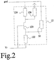
- Figure 2 shows an improved bias stage 12 as a replacement of the bias stage 12 of figure 1 .
- a first resistor 20 has been added, coupled between ground and a node between the source of bias transistor 120 and source resistor 122.
- First resistor 20 serves to compensate for power supply deviations.
- the bias stage 12 still serves to compensate for threshold voltage deviations, but without pinching off amplifying transistor 104.
- the coupling of the node to gnd via first resistor 20 serves to affect an offset in the bias voltage at the gate of amplifier transistor 104 (not shown in figure 2 ).
- First resistor 20 may be coupled to any power supply voltage connection that supplies a higher power supply voltage than the negative power supply voltage connection V- (to gnd in the figure, but alternatively a coupling to V+ may be used). Because part of the current through source resistor 122 flows through first resistor 20, the current through drain resistor 124 is less than the current through source resistor 122, which leads to a less negative bias voltage for amplifier transistor 104.
- bias stage 12 Operation of bias stage 12 can be described by a number of equations.
- the threshold voltage deviation compensation is determined by setting the gain "g" of bias stage 12 to a desired value.
- the dependence on the source resistor value Rs of source resistor 122 is changed.
- the gain "g” depends on the effective resistance Rq coupled to the source of bias transistor 120.
- g ⁇ s Rd / 1 + sRq
- the voltage effect of connection of first resistor 20 to ground can be modelled as the addition of a virtual voltage source in series with the effective resistance Rq and with its negative terminal connected to V-.
- the voltage Vq of this virtual voltage source returns with a factor "-g" in the bias voltage and is used to set the absolute value of the bias voltage.
- the voltage Vq corresponds to the hypothetical voltage that would appear at the source of bias transistor 120 if the source current would be zero.
- the resistance values Rs and R20 (of first resistor 20) are preferably selected so that a desired offset gVq in the bias voltage is realized.
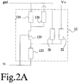
- Figure 2A shows an alternative wherein a second resistor 22 has been added, coupled between the source of bias transistor 120 and the positive power supply connection V+.
- This resistor has a similar effect as first resistor 20. It may be used in combination with or instead of first resistor, taking account of the fact that it changes the effective source resistance Rq (e.g. the parallel circuit of Rs, R20 and R22) and the changed voltage source voltage Vq.
- the additional resistor may be used to compensate for the effect of negative power supply voltage deviations on the bias voltage. This effect arises when bias transistor 120 does not behave as a perfect current source, i.e. when it's drain current depends on it's source drain voltage for a given gate source voltage.
- a change in the negative power supply voltage affects Vq, which in turn affects the bias voltage of amplifier transistor 104 in the opposite direction compared to the imperfect current source behaviour of bias transistor 120.
- the bias stage as described so far, is used to realize a desired gain "g” (preferably minus one) and a desired offset (approximately gVq). These effects depend on three parameters that are freely selectable within certain bounds: the resistance values of first and/or second resistor 20, 22 and the transconductance s of bias transistor 120.
- the combination of the values of these parameters can be selected so that the effect of negative power supply voltage deviations on the bias voltage of amplifier transistor 104 is compensated in combination with setting a desired gain g and offset voltage and in combination with full compensation of threshold voltage variations.
- the desired parameter values can be easily selected using simulation of experimentation for example by first selecting a set of parameters that realizes the required gain and offset and then making successive changes to pairs of the parameters with mutually compensating effect on the gain and offset, until a desired negative supply voltage compensation is realized.
- the design freedom afforded by the bias stage of figures 2 , 2A can be used further to compensate for positive power supply voltage effects on the gain of the amplifier stage. It has been found that high frequency gain of some amplifier transistors 104 increases with decreasing positive power supply voltage V+. In a further embodiment this effect is compensated by lowering the gate bias of amplifier transistor 104 when the positive power supply voltage V+ decreases. This is realized by second resistor 22, which has the effect that Vq drops with decreasing positive power supply voltage V+. In turn a decreased Vq leads to a lower gate bias voltage for amplifier transistor 104.
- the desired amount of lowering of the gate bias with decreasing positive power supply voltage V+ depends on properties of amplifier transistor 104.
- the effect of the power supply voltage V+ on the gain should be substantially equal but opposite to the effect of changed bias voltage.
- the desired power supply voltage V+ sensitivity of the bias voltage that can be derived from this the values of the first and second resistor 20, 22, the source resistor value Rs and the transconductance s of bias transistor can be selected.
- the desired parameter values are preferably selected using simulation of experimentation.
- resistors 20, 22 to the ground and the positive power supply connection (V+) have been used, it should be appreciated that more complex resistance networks may be used instead, or that such a resistor may be connected to the ground or the positive power supply connection via some other nodes that defines a supply voltage or current, such as a node in a voltage divider circuit or a voltage reference circuit.
- the gate of bias transistor 120 has been shown coupled directly to the second power supply connection V- directly, it should be appreciated that alternatively other forms of coupling may be used, for example via some resistance circuit or another high frequency blocking circuit.
- resistors 20, 22 are connected directly to the source of bias transistor 120, it should be appreciated that a more indirect connection may be used with the same effect.
- source resistor 122 a series arrangement of resistors may be used, in which case first resistor 20 and/or second resistor 22 may be coupled to a node inside this series arrangement.
- first resistor 20 and second resistor 22 may be coupled to the source (or such a node) in common via a further resistor (not shown).
- transistors of the opposite conductivity type may be used if the role of the positive and negative power supply voltages is exchanged.
- resistors and capacitors have been shown, it should be appreciated that in practice some or all of these components may be implemented using transistors or other devices in a circuit configuration that makes them provide the same relevant circuit properties as a resistance or capacitor. In general any circuit with resistance properties, such as a resistor, a network of resistors and/or a transistor configured to have the same relevant properties as a resistance will be termed resistance herein.
Landscapes
- Engineering & Computer Science (AREA)
- Power Engineering (AREA)
- Amplifiers (AREA)
Claims (7)
- Verstärkerschaltung, umfassend:- eine Verstärkerstufe (10), umfassend einen Verstärkertransistor (104) mit einem Gate, gekoppelt an einen Eingang (100) der Verstärkerstufe (10); eine Quelle, gekoppelt an einen Referenzanschluss (gnd) und einen Abfluss, gekoppelt an einen ersten Stromversorgungsanschluss (V+), und- eine Bias-Stufe (12), umfassend einen Bias-Transistor (120), einen Abflusswiderstand (124) und einen Quellenwiderstand (122), welcher Bias-Transistor (120) ein Gate hat, gekoppelt an einen zweiten Stromversorgungsanschluss (V-) zum Liefern einer Spannung mit entgegengesetzter Polarität in Bezug auf den Referenzanschluss (gnd) verglichen mit dem ersten Stromversorgungsanschluss (V+), eine Quelle, gekoppelt an den zweiten Stromversorgungsanschluss (V-) über den Quellenwiderstand (122), sodass ein Spannungsabfall über den Quellenwiderstand (122) mindestens teilweise eine Gate-Quellenspannung des Bias-Transistors (120) definiert, und einen Abfluss, gekoppelt an den Referenzanschluss (gnd) über den Abflusswiderstand (124) und an das Gate des Verstärkertransistors (104);
dadurch gekennzeichnet, dass die Bias-Stufe einen Widerstand umfasst, einen Widerstand implementiert unter Verwendung eines Transistors oder eines Widerstandsnetzwerks (20,22), gekoppelt von einem Schaltungsknoten, der eine Spannung trägt mit einer gleichen Polarität relativ zu dem zweiten Stromversorgungsanschluss wie der erste Stromversorgungsanschluss, an einen Knoten zwischen der Quelle des Bias-Transistors (120) und dem Quellenwiderstand (122) zum Injizieren von Strom durch den Quellenwiderstand zusätzlich zu Strom, der von dem Abflusswiderstand stammt. - Verstärkerschaltung nach Anspruch 1, wobei der Widerstand, Widerstand implementiert unter Verwendung eines Transistors oder Widerstandsnetzwerks (20), gekoppelt ist an den Referenzanschluss zum Injizieren des Stroms durch einen Quellenwiderstand von dem Referenzanschluss zusätzlich zu Strom, der von dem Abflusswiderstand stammt.
- Verstärkerschaltung nach Anspruch 1, wobei der Widerstand, Widerstand implementiert unter Verwendung eines Transistors oder Widerstandsnetzwerks (22), gekoppelt ist an den ersten Stromversorgungsanschluss zum Injizieren des Stroms durch den Quellenwiderstand von dem ersten Stromversorgungsanschluss zusätzlich zu Strom, der von dem Abflusswiderstand stammt.
- Verstärkerschaltung nach Anspruch 3, umfassend einen zweiten Widerstand, Widerstand implementiert unter Verwendung eines Transistors oder Widerstandsnetzwerks (20), gekoppelt an den Referenzanschluss.
- Verstärkungsschaltung nach Anspruch 4, wobei Widerstandswerte des Widerstands oder Widerstandsnetzwerks (22) und des zweiten Widerstands, Widerstand implementiert unter Verwendung eines Transistors oder Widerstandsnetzwerks (22), so ausgewählt wurden, dass im Wesentlichen jede Gate-Spannungsschwankung an dem Gate des Verstärkertransistors (104) aufgrund von Stromversorgungsspannungsschwankung auf dem zweiten Stromversorgungsanschuss (V-) ausgeglichen wird.
- Verstärkerschaltung nach Anspruch 4, wobei Widerstandswerte des Widerstands, Widerstand implementiert unter Verwendung eines Transistors oder Widerstandsnetzwerks (22), und des zweiten Widerstands, Widerstand implementiert unter Verwendung eines Transistors oder Widerstandsnetzwerks (20), so ausgewählt wurden, dass eine Spannungsdifferenz zwischen dem Gate von Verstärkertransistor (104) und dem Referenzanschluss (gnd) abnimmt als Reaktion auf erhöhte Spannungsdifferenz zwischen dem ersten Stromversorgungsanschluss (V+) und dem Referenzanschluss (gnd).
- Verstärkerschaltung nach Anspruch 1, wobei der Widerstand, Widerstand implementiert unter Verwendung eines Transistors oder Widerstandsnetzwerks, angeschlossen ist an den Referenzanschluss oder den ersten Stromversorgungsanschluss über einen Knoten in einer Spannungsteilerschaltung oder einer Spannungsreferenzschaltung.
Priority Applications (1)
| Application Number | Priority Date | Filing Date | Title |
|---|---|---|---|
| EP06824286.6A EP1969718B1 (de) | 2005-12-02 | 2006-12-04 | Verstärker mit kompensierter gatearbeitsspannung |
Applications Claiming Priority (3)
| Application Number | Priority Date | Filing Date | Title |
|---|---|---|---|
| EP05077761A EP1793491A1 (de) | 2005-12-02 | 2005-12-02 | Verstärker mit kompensierter Gatearbeitsspannung |
| PCT/NL2006/000608 WO2007064201A1 (en) | 2005-12-02 | 2006-12-04 | Amplifier with compensated gate bias |
| EP06824286.6A EP1969718B1 (de) | 2005-12-02 | 2006-12-04 | Verstärker mit kompensierter gatearbeitsspannung |
Publications (2)
| Publication Number | Publication Date |
|---|---|
| EP1969718A1 EP1969718A1 (de) | 2008-09-17 |
| EP1969718B1 true EP1969718B1 (de) | 2018-09-05 |
Family
ID=36178200
Family Applications (2)
| Application Number | Title | Priority Date | Filing Date |
|---|---|---|---|
| EP05077761A Withdrawn EP1793491A1 (de) | 2005-12-02 | 2005-12-02 | Verstärker mit kompensierter Gatearbeitsspannung |
| EP06824286.6A Active EP1969718B1 (de) | 2005-12-02 | 2006-12-04 | Verstärker mit kompensierter gatearbeitsspannung |
Family Applications Before (1)
| Application Number | Title | Priority Date | Filing Date |
|---|---|---|---|
| EP05077761A Withdrawn EP1793491A1 (de) | 2005-12-02 | 2005-12-02 | Verstärker mit kompensierter Gatearbeitsspannung |
Country Status (5)
| Country | Link |
|---|---|
| US (1) | US7961049B2 (de) |
| EP (2) | EP1793491A1 (de) |
| CA (1) | CA2631801C (de) |
| IL (1) | IL191858A (de) |
| WO (1) | WO2007064201A1 (de) |
Families Citing this family (7)
| Publication number | Priority date | Publication date | Assignee | Title |
|---|---|---|---|---|
| DE10352993A1 (de) | 2003-11-13 | 2005-06-16 | Braun Gmbh | Bürstenteil für eine elektrische Zahnbürste |
| EP2184850A1 (de) * | 2008-11-10 | 2010-05-12 | Nederlandse Organisatie voor toegepast-natuurwetenschappelijk Onderzoek TNO | Vorgespannter Leistungsverstärker |
| US8949083B2 (en) * | 2011-07-29 | 2015-02-03 | Globalfoundries Inc. | Modeling gate transconductance in a sub-circuit transistor model |
| DE102015002501B3 (de) * | 2015-02-27 | 2016-07-07 | Dialog Semiconductor (Uk) Limited | Anstiegsraten- und Einschaltstrom-Controller |
| US9520836B1 (en) | 2015-08-13 | 2016-12-13 | Raytheon Company | Multi-stage amplifier with cascode stage and DC bias regulator |
| US9584072B1 (en) | 2015-08-13 | 2017-02-28 | Raytheon Company | DC bias regulator for cascode amplifier |
| US12135574B2 (en) | 2022-08-05 | 2024-11-05 | Semtech Corporation | Biasing control for compound semiconductors |
Family Cites Families (6)
| Publication number | Priority date | Publication date | Assignee | Title |
|---|---|---|---|---|
| JPH0793410B2 (ja) * | 1987-12-28 | 1995-10-09 | 三菱電機株式会社 | 半導体装置 |
| JPH07202585A (ja) * | 1993-12-28 | 1995-08-04 | Nec Corp | 高周波電力増幅回路 |
| US5506544A (en) * | 1995-04-10 | 1996-04-09 | Motorola, Inc. | Bias circuit for depletion mode field effect transistors |
| JPH09260957A (ja) * | 1996-01-18 | 1997-10-03 | Fujitsu Ltd | 半導体増幅回路 |
| JP2000124749A (ja) * | 1998-10-16 | 2000-04-28 | Matsushita Electric Ind Co Ltd | 半導体集積装置 |
| JP2005223437A (ja) | 2004-02-03 | 2005-08-18 | Nec Compound Semiconductor Devices Ltd | バイアス回路 |
-
2005
- 2005-12-02 EP EP05077761A patent/EP1793491A1/de not_active Withdrawn
-
2006
- 2006-12-04 EP EP06824286.6A patent/EP1969718B1/de active Active
- 2006-12-04 WO PCT/NL2006/000608 patent/WO2007064201A1/en not_active Ceased
- 2006-12-04 US US12/095,731 patent/US7961049B2/en active Active
- 2006-12-04 CA CA2631801A patent/CA2631801C/en active Active
-
2008
- 2008-06-01 IL IL191858A patent/IL191858A/en active IP Right Grant
Also Published As
| Publication number | Publication date |
|---|---|
| EP1969718A1 (de) | 2008-09-17 |
| CA2631801C (en) | 2015-09-22 |
| WO2007064201A1 (en) | 2007-06-07 |
| IL191858A (en) | 2013-11-28 |
| US7961049B2 (en) | 2011-06-14 |
| IL191858A0 (en) | 2008-12-29 |
| US20100066453A1 (en) | 2010-03-18 |
| CA2631801A1 (en) | 2007-06-07 |
| EP1793491A1 (de) | 2007-06-06 |
Similar Documents
| Publication | Publication Date | Title |
|---|---|---|
| US11099590B2 (en) | Indirect leakage compensation for multi-stage amplifiers | |
| JP5012412B2 (ja) | 増幅装置及びバイアス回路 | |
| US7504874B2 (en) | Transistor arrangement with temperature compensation and method for temperature compensation | |
| US20020113652A1 (en) | Amplifier circuit | |
| IL191858A (en) | Amplifier with tilted compensated gate | |
| US6717467B2 (en) | Wideband differential amplifier comprising a high frequency gain-drop compensator device | |
| US7312660B2 (en) | Differential amplifier and active load for the same | |
| US7215200B1 (en) | High-linearity differential amplifier with flexible common-mode range | |
| US6538513B2 (en) | Common mode output current control circuit and method | |
| CN106774572A (zh) | 米勒补偿电路及电子电路 | |
| US10574200B2 (en) | Transconductance amplifier | |
| US20040124918A1 (en) | Wideband common-mode regulation circuit | |
| US20100134188A1 (en) | Buffer amplifier | |
| JP4401776B2 (ja) | 自動バイアス供給源調節機構を有する可変利得増幅器 | |
| KR100499858B1 (ko) | 가변 이득 증폭기 | |
| US7378908B2 (en) | Variable gain differential amplifier, and variable degeneration impedance control device and method for use in the same | |
| US7629846B2 (en) | Source follower circuit and semiconductor apparatus | |
| CN117674745A (zh) | 放大电路和通信装置 | |
| EP1790074B1 (de) | Linear-transkonduktanz-zelle mit grossem abstimmbereich | |
| EP3334039B1 (de) | Quellenverfolger | |
| WO2006036060A1 (en) | Gate bias generator | |
| JP4071146B2 (ja) | バッファ回路 | |
| CN118282331A (zh) | 两级共模反馈电路及包括其的全差分运算放大器 | |
| CN115443609A (zh) | 放大装置 | |
| KR19990061179A (ko) | 고출력증폭기의 온도보상 바이어스회로 |
Legal Events
| Date | Code | Title | Description |
|---|---|---|---|
| PUAI | Public reference made under article 153(3) epc to a published international application that has entered the european phase |
Free format text: ORIGINAL CODE: 0009012 |
|
| 17P | Request for examination filed |
Effective date: 20080701 |
|
| AK | Designated contracting states |
Kind code of ref document: A1 Designated state(s): AT BE BG CH CY CZ DE DK EE ES FI FR GB GR HU IE IS IT LI LT LU LV MC NL PL PT RO SE SI SK TR |
|
| 17Q | First examination report despatched |
Effective date: 20120525 |
|
| DAX | Request for extension of the european patent (deleted) | ||
| RAP1 | Party data changed (applicant data changed or rights of an application transferred) |
Owner name: NEDERLANDSE ORGANISATIE VOOR TOEGEPAST- NATUURWETE |
|
| GRAP | Despatch of communication of intention to grant a patent |
Free format text: ORIGINAL CODE: EPIDOSNIGR1 |
|
| RIC1 | Information provided on ipc code assigned before grant |
Ipc: H03F 3/193 20060101ALI20180228BHEP Ipc: H03F 1/30 20060101AFI20180228BHEP |
|
| INTG | Intention to grant announced |
Effective date: 20180328 |
|
| GRAS | Grant fee paid |
Free format text: ORIGINAL CODE: EPIDOSNIGR3 |
|
| GRAA | (expected) grant |
Free format text: ORIGINAL CODE: 0009210 |
|
| AK | Designated contracting states |
Kind code of ref document: B1 Designated state(s): AT BE BG CH CY CZ DE DK EE ES FI FR GB GR HU IE IS IT LI LT LU LV MC NL PL PT RO SE SI SK TR |
|
| REG | Reference to a national code |
Ref country code: GB Ref legal event code: FG4D |
|
| REG | Reference to a national code |
Ref country code: CH Ref legal event code: EP |
|
| REG | Reference to a national code |
Ref country code: AT Ref legal event code: REF Ref document number: 1039026 Country of ref document: AT Kind code of ref document: T Effective date: 20180915 |
|
| REG | Reference to a national code |
Ref country code: DE Ref legal event code: R096 Ref document number: 602006056272 Country of ref document: DE |
|
| REG | Reference to a national code |
Ref country code: IE Ref legal event code: FG4D |
|
| REG | Reference to a national code |
Ref country code: NL Ref legal event code: FP |
|
| REG | Reference to a national code |
Ref country code: LT Ref legal event code: MG4D |
|
| PG25 | Lapsed in a contracting state [announced via postgrant information from national office to epo] |
Ref country code: FI Free format text: LAPSE BECAUSE OF FAILURE TO SUBMIT A TRANSLATION OF THE DESCRIPTION OR TO PAY THE FEE WITHIN THE PRESCRIBED TIME-LIMIT Effective date: 20180905 Ref country code: GR Free format text: LAPSE BECAUSE OF FAILURE TO SUBMIT A TRANSLATION OF THE DESCRIPTION OR TO PAY THE FEE WITHIN THE PRESCRIBED TIME-LIMIT Effective date: 20181206 Ref country code: BG Free format text: LAPSE BECAUSE OF FAILURE TO SUBMIT A TRANSLATION OF THE DESCRIPTION OR TO PAY THE FEE WITHIN THE PRESCRIBED TIME-LIMIT Effective date: 20181205 Ref country code: SE Free format text: LAPSE BECAUSE OF FAILURE TO SUBMIT A TRANSLATION OF THE DESCRIPTION OR TO PAY THE FEE WITHIN THE PRESCRIBED TIME-LIMIT Effective date: 20180905 Ref country code: LT Free format text: LAPSE BECAUSE OF FAILURE TO SUBMIT A TRANSLATION OF THE DESCRIPTION OR TO PAY THE FEE WITHIN THE PRESCRIBED TIME-LIMIT Effective date: 20180905 |
|
| REG | Reference to a national code |
Ref country code: AT Ref legal event code: MK05 Ref document number: 1039026 Country of ref document: AT Kind code of ref document: T Effective date: 20180905 |
|
| PG25 | Lapsed in a contracting state [announced via postgrant information from national office to epo] |
Ref country code: LV Free format text: LAPSE BECAUSE OF FAILURE TO SUBMIT A TRANSLATION OF THE DESCRIPTION OR TO PAY THE FEE WITHIN THE PRESCRIBED TIME-LIMIT Effective date: 20180905 Ref country code: ES Free format text: LAPSE BECAUSE OF FAILURE TO SUBMIT A TRANSLATION OF THE DESCRIPTION OR TO PAY THE FEE WITHIN THE PRESCRIBED TIME-LIMIT Effective date: 20180905 |
|
| PG25 | Lapsed in a contracting state [announced via postgrant information from national office to epo] |
Ref country code: CZ Free format text: LAPSE BECAUSE OF FAILURE TO SUBMIT A TRANSLATION OF THE DESCRIPTION OR TO PAY THE FEE WITHIN THE PRESCRIBED TIME-LIMIT Effective date: 20180905 Ref country code: IS Free format text: LAPSE BECAUSE OF FAILURE TO SUBMIT A TRANSLATION OF THE DESCRIPTION OR TO PAY THE FEE WITHIN THE PRESCRIBED TIME-LIMIT Effective date: 20190105 Ref country code: PL Free format text: LAPSE BECAUSE OF FAILURE TO SUBMIT A TRANSLATION OF THE DESCRIPTION OR TO PAY THE FEE WITHIN THE PRESCRIBED TIME-LIMIT Effective date: 20180905 Ref country code: RO Free format text: LAPSE BECAUSE OF FAILURE TO SUBMIT A TRANSLATION OF THE DESCRIPTION OR TO PAY THE FEE WITHIN THE PRESCRIBED TIME-LIMIT Effective date: 20180905 Ref country code: EE Free format text: LAPSE BECAUSE OF FAILURE TO SUBMIT A TRANSLATION OF THE DESCRIPTION OR TO PAY THE FEE WITHIN THE PRESCRIBED TIME-LIMIT Effective date: 20180905 Ref country code: AT Free format text: LAPSE BECAUSE OF FAILURE TO SUBMIT A TRANSLATION OF THE DESCRIPTION OR TO PAY THE FEE WITHIN THE PRESCRIBED TIME-LIMIT Effective date: 20180905 Ref country code: IT Free format text: LAPSE BECAUSE OF FAILURE TO SUBMIT A TRANSLATION OF THE DESCRIPTION OR TO PAY THE FEE WITHIN THE PRESCRIBED TIME-LIMIT Effective date: 20180905 |
|
| PG25 | Lapsed in a contracting state [announced via postgrant information from national office to epo] |
Ref country code: SK Free format text: LAPSE BECAUSE OF FAILURE TO SUBMIT A TRANSLATION OF THE DESCRIPTION OR TO PAY THE FEE WITHIN THE PRESCRIBED TIME-LIMIT Effective date: 20180905 Ref country code: PT Free format text: LAPSE BECAUSE OF FAILURE TO SUBMIT A TRANSLATION OF THE DESCRIPTION OR TO PAY THE FEE WITHIN THE PRESCRIBED TIME-LIMIT Effective date: 20190105 |
|
| REG | Reference to a national code |
Ref country code: DE Ref legal event code: R097 Ref document number: 602006056272 Country of ref document: DE |
|
| PLBE | No opposition filed within time limit |
Free format text: ORIGINAL CODE: 0009261 |
|
| STAA | Information on the status of an ep patent application or granted ep patent |
Free format text: STATUS: NO OPPOSITION FILED WITHIN TIME LIMIT |
|
| PG25 | Lapsed in a contracting state [announced via postgrant information from national office to epo] |
Ref country code: DK Free format text: LAPSE BECAUSE OF FAILURE TO SUBMIT A TRANSLATION OF THE DESCRIPTION OR TO PAY THE FEE WITHIN THE PRESCRIBED TIME-LIMIT Effective date: 20180905 |
|
| REG | Reference to a national code |
Ref country code: CH Ref legal event code: PL |
|
| 26N | No opposition filed |
Effective date: 20190606 |
|
| PG25 | Lapsed in a contracting state [announced via postgrant information from national office to epo] |
Ref country code: SI Free format text: LAPSE BECAUSE OF FAILURE TO SUBMIT A TRANSLATION OF THE DESCRIPTION OR TO PAY THE FEE WITHIN THE PRESCRIBED TIME-LIMIT Effective date: 20180905 Ref country code: LU Free format text: LAPSE BECAUSE OF NON-PAYMENT OF DUE FEES Effective date: 20181204 Ref country code: MC Free format text: LAPSE BECAUSE OF FAILURE TO SUBMIT A TRANSLATION OF THE DESCRIPTION OR TO PAY THE FEE WITHIN THE PRESCRIBED TIME-LIMIT Effective date: 20180905 |
|
| REG | Reference to a national code |
Ref country code: IE Ref legal event code: MM4A |
|
| REG | Reference to a national code |
Ref country code: BE Ref legal event code: MM Effective date: 20181231 |
|
| PG25 | Lapsed in a contracting state [announced via postgrant information from national office to epo] |
Ref country code: IE Free format text: LAPSE BECAUSE OF NON-PAYMENT OF DUE FEES Effective date: 20181204 |
|
| PG25 | Lapsed in a contracting state [announced via postgrant information from national office to epo] |
Ref country code: BE Free format text: LAPSE BECAUSE OF NON-PAYMENT OF DUE FEES Effective date: 20181231 |
|
| PG25 | Lapsed in a contracting state [announced via postgrant information from national office to epo] |
Ref country code: CH Free format text: LAPSE BECAUSE OF NON-PAYMENT OF DUE FEES Effective date: 20181231 Ref country code: LI Free format text: LAPSE BECAUSE OF NON-PAYMENT OF DUE FEES Effective date: 20181231 |
|
| PG25 | Lapsed in a contracting state [announced via postgrant information from national office to epo] |
Ref country code: TR Free format text: LAPSE BECAUSE OF FAILURE TO SUBMIT A TRANSLATION OF THE DESCRIPTION OR TO PAY THE FEE WITHIN THE PRESCRIBED TIME-LIMIT Effective date: 20180905 |
|
| PG25 | Lapsed in a contracting state [announced via postgrant information from national office to epo] |
Ref country code: HU Free format text: LAPSE BECAUSE OF FAILURE TO SUBMIT A TRANSLATION OF THE DESCRIPTION OR TO PAY THE FEE WITHIN THE PRESCRIBED TIME-LIMIT; INVALID AB INITIO Effective date: 20061204 Ref country code: CY Free format text: LAPSE BECAUSE OF FAILURE TO SUBMIT A TRANSLATION OF THE DESCRIPTION OR TO PAY THE FEE WITHIN THE PRESCRIBED TIME-LIMIT Effective date: 20180905 |
|
| P01 | Opt-out of the competence of the unified patent court (upc) registered |
Effective date: 20230522 |
|
| PGFP | Annual fee paid to national office [announced via postgrant information from national office to epo] |
Ref country code: DE Payment date: 20241210 Year of fee payment: 19 |
|
| PGFP | Annual fee paid to national office [announced via postgrant information from national office to epo] |
Ref country code: NL Payment date: 20241219 Year of fee payment: 19 |
|
| PGFP | Annual fee paid to national office [announced via postgrant information from national office to epo] |
Ref country code: GB Payment date: 20241224 Year of fee payment: 19 |
|
| PGFP | Annual fee paid to national office [announced via postgrant information from national office to epo] |
Ref country code: FR Payment date: 20241223 Year of fee payment: 19 |