EP1944817A2 - Method of manufacturing flat panel display device - Google Patents
Method of manufacturing flat panel display device Download PDFInfo
- Publication number
- EP1944817A2 EP1944817A2 EP07252499A EP07252499A EP1944817A2 EP 1944817 A2 EP1944817 A2 EP 1944817A2 EP 07252499 A EP07252499 A EP 07252499A EP 07252499 A EP07252499 A EP 07252499A EP 1944817 A2 EP1944817 A2 EP 1944817A2
- Authority
- EP
- European Patent Office
- Prior art keywords
- substrate
- light emitting
- laser
- intensity
- emitting units
- Prior art date
- Legal status (The legal status is an assumption and is not a legal conclusion. Google has not performed a legal analysis and makes no representation as to the accuracy of the status listed.)
- Granted
Links
Images


Classifications
-
- H—ELECTRICITY
- H10—SEMICONDUCTOR DEVICES; ELECTRIC SOLID-STATE DEVICES NOT OTHERWISE PROVIDED FOR
- H10K—ORGANIC ELECTRIC SOLID-STATE DEVICES
- H10K59/00—Integrated devices, or assemblies of multiple devices, comprising at least one organic light-emitting element covered by group H10K50/00
- H10K59/80—Constructional details
- H10K59/87—Passivation; Containers; Encapsulations
- H10K59/871—Self-supporting sealing arrangements
-
- E—FIXED CONSTRUCTIONS
- E03—WATER SUPPLY; SEWERAGE
- E03B—INSTALLATIONS OR METHODS FOR OBTAINING, COLLECTING, OR DISTRIBUTING WATER
- E03B7/00—Water main or service pipe systems
- E03B7/07—Arrangement of devices, e.g. filters, flow controls, measuring devices, siphons or valves, in the pipe systems
- E03B7/072—Arrangement of flowmeters
-
- H—ELECTRICITY
- H10—SEMICONDUCTOR DEVICES; ELECTRIC SOLID-STATE DEVICES NOT OTHERWISE PROVIDED FOR
- H10K—ORGANIC ELECTRIC SOLID-STATE DEVICES
- H10K50/00—Organic light-emitting devices
- H10K50/80—Constructional details
- H10K50/84—Passivation; Containers; Encapsulations
- H10K50/841—Self-supporting sealing arrangements
-
- H—ELECTRICITY
- H10—SEMICONDUCTOR DEVICES; ELECTRIC SOLID-STATE DEVICES NOT OTHERWISE PROVIDED FOR
- H10K—ORGANIC ELECTRIC SOLID-STATE DEVICES
- H10K50/00—Organic light-emitting devices
- H10K50/80—Constructional details
- H10K50/84—Passivation; Containers; Encapsulations
- H10K50/842—Containers
- H10K50/8426—Peripheral sealing arrangements, e.g. adhesives, sealants
-
- H—ELECTRICITY
- H10—SEMICONDUCTOR DEVICES; ELECTRIC SOLID-STATE DEVICES NOT OTHERWISE PROVIDED FOR
- H10K—ORGANIC ELECTRIC SOLID-STATE DEVICES
- H10K59/00—Integrated devices, or assemblies of multiple devices, comprising at least one organic light-emitting element covered by group H10K50/00
- H10K59/80—Constructional details
- H10K59/87—Passivation; Containers; Encapsulations
- H10K59/871—Self-supporting sealing arrangements
- H10K59/8722—Peripheral sealing arrangements, e.g. adhesives, sealants
-
- H—ELECTRICITY
- H10—SEMICONDUCTOR DEVICES; ELECTRIC SOLID-STATE DEVICES NOT OTHERWISE PROVIDED FOR
- H10K—ORGANIC ELECTRIC SOLID-STATE DEVICES
- H10K71/00—Manufacture or treatment specially adapted for the organic devices covered by this subclass
-
- H—ELECTRICITY
- H10—SEMICONDUCTOR DEVICES; ELECTRIC SOLID-STATE DEVICES NOT OTHERWISE PROVIDED FOR
- H10K—ORGANIC ELECTRIC SOLID-STATE DEVICES
- H10K71/00—Manufacture or treatment specially adapted for the organic devices covered by this subclass
- H10K71/40—Thermal treatment, e.g. annealing in the presence of a solvent vapour
-
- F—MECHANICAL ENGINEERING; LIGHTING; HEATING; WEAPONS; BLASTING
- F16—ENGINEERING ELEMENTS AND UNITS; GENERAL MEASURES FOR PRODUCING AND MAINTAINING EFFECTIVE FUNCTIONING OF MACHINES OR INSTALLATIONS; THERMAL INSULATION IN GENERAL
- F16L—PIPES; JOINTS OR FITTINGS FOR PIPES; SUPPORTS FOR PIPES, CABLES OR PROTECTIVE TUBING; MEANS FOR THERMAL INSULATION IN GENERAL
- F16L55/00—Devices or appurtenances for use in, or in connection with, pipes or pipe systems
- F16L55/02—Energy absorbers; Noise absorbers
-
- H—ELECTRICITY
- H10—SEMICONDUCTOR DEVICES; ELECTRIC SOLID-STATE DEVICES NOT OTHERWISE PROVIDED FOR
- H10K—ORGANIC ELECTRIC SOLID-STATE DEVICES
- H10K59/00—Integrated devices, or assemblies of multiple devices, comprising at least one organic light-emitting element covered by group H10K50/00
- H10K59/10—OLED displays
-
- H—ELECTRICITY
- H10—SEMICONDUCTOR DEVICES; ELECTRIC SOLID-STATE DEVICES NOT OTHERWISE PROVIDED FOR
- H10K—ORGANIC ELECTRIC SOLID-STATE DEVICES
- H10K71/00—Manufacture or treatment specially adapted for the organic devices covered by this subclass
- H10K71/50—Forming devices by joining two substrates together, e.g. lamination techniques
-
- H—ELECTRICITY
- H10—SEMICONDUCTOR DEVICES; ELECTRIC SOLID-STATE DEVICES NOT OTHERWISE PROVIDED FOR
- H10K—ORGANIC ELECTRIC SOLID-STATE DEVICES
- H10K71/00—Manufacture or treatment specially adapted for the organic devices covered by this subclass
- H10K71/851—Division of substrate
Definitions
- the present invention relates to a method of manufacturing a flat panel display device, and more particularly, to a method of manufacturing a flat panel display device that is sealed by glass frits.
- flat panel display devices such as organic light emitting display devices and TFT-LCDs can be made thin and flexible, and thus, much research into such flat panel display devices is being conducted.
- Organic light emitting display devices deteriorate as moisture penetrates therein, so that a sealing structure for preventing penetration of moisture is required.
- a metal can or a glass substrate that is processed to a cap shape with a groove has been used as a sealing member.
- the metal can or glass substrate may contain a desiccant in powder form for absorbing moisture once it is sealed.
- a desiccant film may be attached to the sealing member using, e.g., a double-sided tape.
- the sealing member is combined with a substrate, on which a light emitting element is formed, using a UV curable organic sealant or a thermo-curable organic sealant.
- glass frits with a high resistance to pressure and good sealing characteristics have been suggested as a substitute for organic sealants.
- a laser can be used to melt the glass frits and reduce thermal effects on the organic light emitting element.
- cut faces of the glass may deteriorate due to the thermal stresses generated by radiation of the laser.
- the temperature When melting the glass frit by laser, the temperature instantaneously rises to a high temperature of about 500-600°C, which thermally impacts the glass. Such a thermal impact leads to a deviation in stress between parts of the glass, so that cracks occur in an unintended direction when cutting the glass. As a result, protrusions, particles, etc., are generated on a cut face of the glass.
- An object of the present invention is to provide a method of manufacturing a flat panel display device by combining a substrate and a sealing member via glass frits that are melted by a laser, to minimise the formation of interior cut faces when the substrate is cut into separate devices.
- the present invention provides a method of manufacturing a flat panel display device according to claim 1.
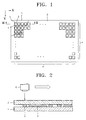
- FIG. 1 is a plan view of substrates for a flat panel display device to be manufactured by a method according to an embodiment of the present invention.
- FIG. 2 is a sectional view of the substrates taken along line II-II in FIG. 1 .
- FIG. 3 is a sectional view of the substrates taken along line II-II in FIG. 1 when an annealing process is performed.
- FIG. 4 is a sectional view of an example of a light emitting unit in FIG. 1 .
- FIG. 5 is a schematic plan view illustrating the shape of protrusions that are formed on a cut face of a second substrate when the second substrate is cut immediately after a substrate combining process.
- FIG. 6 is a schematic plan view illustrating the shape of protrusions that are formed on a cut face of a second substrate when the second substrate is cut after an annealing process.
- FIG. 7 is a photograph of a cut face of a second substrate that is cut immediately after a substrate combining process is performed without an annealing process.
- FIG. 8 is a photograph of a cut face of a second substrate that is cut immediately after a substrate combining process is performed without an annealing process, showing cracking on the second substrate.
- FIG. 9 is a photograph of a cut face of a second substrate that is cut after an annealing process.
- FIG. 10 is a schematic view for explaining the order of laser radiation onto cells using a multi-head.
- FIG. 1 is a plan view of substrates for a flat panel display device to be manufactured by a method according to an embodiment of the present invention.
- FIG. 2 is a sectional view taken along line II-II in FIG. 1 .
- a plurality of light emitting units 3 are formed on a surface of the first substrate 1.
- the first substrate 1 and the second substrate may be formed of a transparent glass material, but are not limited thereto.
- Each of the light emitting units 3 includes a plurality of light emitting elements.
- the light emitting units 11 may be organic light emitting units including a plurality of organic light emitting elements.
- FIG. 4 is a sectional view of an active matrix organic light emitting device as an example of the light emitting unit 11.
- an insulating layer 11 such as a barrier layer and/or a buffer layer, which prevents diffusion of impurity ions and permeation of moisture or external air and planarizes the surface of the first substrate 1, may be formed on an upper surface of the first substrate 1.
- An active layer 12 for a TFT is formed of a semiconductor material on the insulating layer 11, and a gate insulating layer 13 is formed so as to cover the active layer 12.
- the active layer 12 may be formed of an inorganic semiconductor material, such as amorphous silicon or polysilicon, or an organic semiconductor material.
- the active layer 12 has a source region 12b, a drain region 12c, and a channel region 12a between the source region 12b and the drain region 12c.
- a gate electrode 14 is formed on the gate insulating layer 13, and an interlayer insulating layer 15 is formed so as to cover the gate electrode 4.
- a source electrode 16a and a drain electrode 16b are formed on the interlayer insulating layer 15.
- a planarization layer 17 and a pixel-defining layer 18 are sequentially formed so as to cover the source electrode 16a and the drain electrode 16b.
- the gate insulating layer 13, the interlayer insulating layer 15, the planarization layer 17, and the pixel-defining layer 18 may be formed of an insulating material in a single- or multi-layered structure, and may be formed of an organic material, an inorganic material, or an organic/inorganic composite material.
- Such a stacked structure of the TFT as described above is not limited thereto, and the TFT may have various structures.
- a pixel electrode 31 of an organic light emitting diode (OLED) is formed on the planarization layer 17, and a pixel-defining layer 18 is formed on the planarization layer 17.
- a predetermined opening is formed in the pixel-defining layer 18 so as to expose the pixel electrode 31, and an organic emitting layer 32 of the OLED is formed.
- the OLED displays predetermined image information by emitting red, green, and blue light according to the flow of current.
- the OLED includes the pixel electrode 31, which contacts the drain electrode 16b of the TFT via a contact hole, an opposing electrode 33 covering all of the pixels, and the organic emitting layer 32 disposed between the pixel electrode 31 and the opposing electrode 33 to emit light.
- the pixel electrode 31 and the opposing electrode 33 are insulated from one another by the organic emitting layer 32, and voltages having different polarities are applied across the pixel electrode 31 and the opposing electrode 33, respectively, to emit light in the organic emitting layer 32.
- the organic emitting layer 32 may be formed of a low-molecular weight organic layer or a polymer organic layer.
- a low-molecular weight organic layer When a low-molecular weight organic layer is used, it may be formed as a hole injection layer (HIL), a hole transport layer (HTL), an emitting layer (EML), a hole transport layer (HTL), an emitting layer (EML), an electron transport layer (ETL), an electron injection layer (ETL), etc., having a single layered structure of a stacked composite structure.
- organic materials examples include copper phthalocyanine (CuPc), N,N'-di(naphthalene-1-yl)-N,N'-diphenyl-benzidine (NPB), tris-8-hydroxyquinoline aluminum (Alq3), etc.
- CuPc copper phthalocyanine
- NPB N,N'-di(naphthalene-1-yl)-N,N'-diphenyl-benzidine
- Alq3 tris-8-hydroxyquinoline aluminum
- the low-molecular weight organic layer may be formed using vacuum deposition.
- the hole injection layer, the hole transport layer, the electron transport layer, the electron injection layer, etc. may be common to red, green, and blue pixels. Accordingly, unlike the structure in FIG. 4 , these common layers may be formed so as to cover the entire pixels, like the opposing electrode 33.
- the pixel electrode 31 functions as an anode, and the opposing electrode 33 functions as a cathode. Alternatively, the polarities of the pixel electrode 31 and the opposing electrode 33 may be reversed.
- the pixel electrode 31 may be a transparent electrode, and the opposing electrode 33 may be a reflective electrode.
- the pixel electrode 31 may be formed of a high-work function material, for example, ITO, IZO, ZnO, In 2 O 3 , etc.
- the opposing electrode 33 may be formed of a small-work function metal, for example, Ag, Mg, Al, Pt, Pd, Au, Ni, Nd, Ir, Cr, Li, Ca, etc.
- the pixel electrode 31 may be formed as a reflective electrode, and the opposing electrode 33 may be formed as a transparent electrode.
- the reflective electrode for the pixel electrode 31 may include a reflective layer formed of Ag, Mg, Al, Pt, Pd, Au, Ni, Nd, Ir, Cr, Li, Ca, a combination thereof, etc., and a high-work function material, for example, ITO, IZO, ZnO, In 2 O 3 , etc.
- the transparent electrode for the opposing electrode 33 may be formed by depositing a small-work function metal, for example, Ag, Mg, Al, Pt, Pd, Au, Ni, Nd, Ir, Cr, Li, Ca, or a combination thereof and forming an auxiliary electrode layer or a bus electrode line thereon using a transparent conductive material, such as ITO, IZO, ZnO, In 2 O 3 , etc.
- a small-work function metal for example, Ag, Mg, Al, Pt, Pd, Au, Ni, Nd, Ir, Cr, Li, Ca, or a combination thereof
- a transparent conductive material such as ITO, IZO, ZnO, In 2 O 3 , etc.
- both the pixel electrode 31 and the opposing electrode 33 may be formed as transparent electrodes.
- the pixel electrode 31 and the opposing electrode 33 may be formed of a conductive organic material, or a conductive paste containing conductive particles, such as Ag, Mg, Cu, etc.
- the pixel electrode 31 and the opposing electrode 33 may be formed by inkjet printing. After the inkjet printing, baking is performed to obtain the electrodes.
- a passivation layer 34 may be further formed on the opposing electrode 33 in the light emitting unit 3 so as to cover the light emitting unit 3.
- the passivation layer 34 may be formed of an inorganic material, an organic material, or organic and inorganic materials stacked upon one another.
- a pad unit 4 connecting each of the light emitting units 3 and an external device may be disposed adjacent to the light emitting unit 3.
- m light emitting units 3 and m pad units 4 are formed in a first direction indicated by X, and n light emitting units 3 and n pad units 4 are formed in a second direction indicated by Y.
- one light emitting unit 3 and one pad unit 4 form a single unit cell.
- the light emitting unit 3 and the pad unit 4 in each unit cell are adjacent to each other in the second direction indicated by Y.
- a paste of glass frits 5 is applied to a surface of the second substrate facing the first substrate so as to be around each of the light emitting units 3, and is primarily subjected to pre-sintering so as to harden the glass frits 5.
- the paste of glass frits 5 may be applied to a surface of the first substrate 1 facing the second substrate 2.
- the paste of glass frits 5 may be applied sequentially applied to each cell using a dispenser, or may be applied simultaneously to all the cells using a screen printing method.
- the first substrate 1 and the second substrate 2 are combined by locally radiating the glass frits 5 using a laser radiator 6.
- the laser can be radiated on the second substrate 2 from an upper direction, but is not limited thereto. Alternatively, the laser may be radiated on the first substrate 1 from a lower direction, or may be radiated simultaneously on the second substrate 2 from the upper direction and the first substrate 1 from the lower direction.
- the laser radiator 6 When the laser radiator 6 has a single radiation head, laser is radiated onto the glass frits 5 around n unit cells arranged in the second direction Y in the first column of m unit cells arranged in the first direction X, and then onto n unit cells arranged in the second direction Y in the second column of m unit Cells arranged in the first direction X. Accordingly, the laser radiator 6 is moved in the first direction X in the laser radiating process.
- the first direction X and the second direction Y may be reversed.
- a laser having a first intensity is radiated.
- the first intensity of the laser varies according to the beam size of the laser and the characteristics of the glass frits.
- the first intensity of the laser may vary according to the composition of the glass frits 5 and the compositions of the first and second substrates 1 and 2 that are combined by the glass frits 5.
- the first intensity of the laser may be high enough to melt the glass frits 5 so as to combine the first and second substrates 1 and 2.
- the first substrate 1 and the second substrate 2 are combined by melting the glass frits 5 by radiating the laser having the first intensity, as shown in FIG. 3 , the first substrate 1 or the second substrate 2 is annealed by radiating a laser having a second intensity onto the glass frits 5.
- the intensity of the laser radiated for the annealing process may differ from the first intensity of the laser radiated to combine the first and second substrates 1 and 2.
- the second intensity of the laser may be smaller than the first intensity of the laser.
- the second intensity of the laser may be from about 70% to about 80% of the first intensity of the laser.
- the laser radiator 6 emits, during a period of time, a first laser beam which is configured to melt the grass frits 5 and combine the first and second substrates 1 and 2.
- the laser radiator 6 further emits, after the period of time, a second laser beam toward an area where the first laser beam was radiated so as to anneal at least one of the first and second substrates.
- the intensity of the second laser beam is less or substantially less than that of the first laser beam.
- the laser having the second intensity may be radiated in a substantially opposite direction to the radiation of the laser having the first intensity.
- the laser having the first intensity is radiated in the first direction X in the process of combining the first and second substrates 1 and 2.
- the direction in which the laser having the second intensity is radiated in the annealing process may be substantially opposite to the first direction X in which the laser having the first intensity is radiated in the process of combining the first and second substrates 1 and 2.
- the laser having the second intensity can be radiated in the annealing process in an opposite direction to the radiation of the laser having the first intensity in the above-described substrate combining process.
- the radiation direction of the laser having the second intensity may be not exactly opposite to the radiation direction of the laser having the second intensity.
- the radiation direction of the laser in the annealing process may be substantially opposite to the radiation direction of the laser in the substrate combining process.
- the radiation direction of the laser in the annealing process may be opposite to the first direction X.
- the annealing process may be performed while varying the direction in which the laser radiator 6 is moved. However, the annealing process may be performed in a condition in which the direction in which the laser radiator 6 is moved is fixed. In this case, only the intensity of the laser is controlled after the first and second substrates 1 and 2 are rotated by 180° .
- FIG. 5 illustrates the direction in which particles or protrusions protrude on a cut face of the second substrate 2 that is cut immediately after the radiation of the laser in the substrate combining process.
- the generation of particles or protrusions on the cut face of the second substrate 2 can be prevented by the above-described annealing process.
- FIG. 2 illustrates the direction in which particles or protrusions protrude on a cut face of the second substrate 2 that is cut after the radiation of the laser in the annealing process.
- cracks may occur in an expected direction so that a smooth cut face can be obtained.
- the intensity of the laser radiated in the annealing process may be smaller than the intensity of the laser radiated in the substrate combining process so as to prevent the glass frits 5 combining the two substrates 1 and 2 from remelting.
- FIG. 7 is a photograph of a cut face of the second substrate 2 that is cut immediately after the substrate combining process is performed without an annealing process.
- FIG. 8 is a photograph of a cut face of the second substrate 2 that is cut after only the substrate combining process, not the annealing process, is performed, showing cracking on the second substrate 2.
- an upper portion that seems to be hatched is a portion into which a cutter is directly inserted, and a lower portion is a portion that is separated due to cracking caused by the insertion of the cutter into the upper portion.
- the portion that is separated due to cracking includes dark portions, indicating that the cut face is not smooth and has protrusions.
- Such irregular protrusions can be removed by a surface polishing process that is performed after the first and second substrates 1 and 2, i.e., the glass, are cut.
- a surface polishing process is a wet process that mostly cannot be used for organic light emitting display devices, which require sealing and avoid wet processes.
- FIG. 8 shows an example of cracking in one direction when an annealing process as in the present invention is not performed. As shown in FIG. 8 , cracks 120 occur from a later laser-sealed portion 100 to an earlier laser-sealed portion 110.
- Such inevitable failures occurring in a substrate combining process using glass frits can be solved by an annealing process as in one embodiment of the present invention, so that a smooth out face can be obtained, as shown in FIG. 9 .
- the laser radiator 6 may have a multi-head having at least two radiating heads.
- FIG. 10 is a schematic view of cells 3' on the first substrate 1, which is subjected to laser radiation, for explaining the order of laser radiation onto cells using a multi-head.
- the glass frits 5 to be subjected to laser radiation are just drawn by line.
- Five rows A to E are arranged in the second direction (Y).
- the multi-head can simultaneously radiate laser onto a total of 5 alternate cells in each row. Accordingly, in the embodiment of FIG. 10 , when radiating a laser onto row A, the laser can be simultaneously radiated onto five odd columns A[o] or five even columns A[e].
- a laser for combining substrates is radiated onto the cells 3' in the odd columns A[o] in row A.
- the heat generated by the radiation of the laser is transmitted to the cells 3' in the even columns A[e] in row A, providing an effect of indirect laser radiation on the cells 3' in the even columns A[e], and thus primarily changing thermal characteristics of the cells 3'.
- the multi-head radiates a laser for combining substrates onto the cells 3' in the even columns A[e] in row A.
- the thermal characteristics of the cells 3' in the even columns A[e] in row A are directly changed by the laser.
- the cells 3' in the even columns A[e] undergo thermal hysterisis twice.
- the cells 3' in the odd columns A[o]) irradiated by the laser for combining substrates underwent serious changes in thermal characteristics, the cells 3' in the odd columns A[o]) are less affected by the heat transmitted when the laser for combining substrates is secondarily radiated onto the cells 3' in the even columns A[e]. Consequently, the glass strength of the second substrate 2 is greater near the cells 3' in the even columns A[e] than near the cells 3' in the odd columns A[o], so that cracking occurs toward the odd columns A[o] when the second substrate 2 is scribed.
- a laser for annealing is radiated onto the cells 3' in an opposite direction to the laser radiation for combining substrates.
- annealing is performed on unit cells in the order of the even columns and odd columns in row E, the even columns and odd columns in row D, and the even columns and odd columns in row A.
- Table 1 shows deviations in cell size in an 8X18 cell array caused due to glass cutting failures when annealing is not performed after a laser for combining substrates is radiated by a multi-head that can simultaneously radiate a laser onto nine rows.
- the 8X18 cell array included 18 columns A to R in the first direction (X) shown in FIG. 10 and 8 rows in the second direction (Y).
- the target cell size was 37.98 mm.
- Table 1 shows that many cells in even columns became larger.
- Table 2 shows cell sizes after annealing is performed in the same manner as in the embodiment of FIG. 10 described above under the same conditions as described in connection with Table 1.
- Table 2 A B C D E F G H I J K L M N O P Q R 1 37.87 37.82 37.92 37.86 37.87 37.83 37.88 37.8 37.82 37.8 37.85 37.81 37.82 37.76 37.79 37.78 37.78 37.84 2 37.92 37.9 37.88 37.83 37.87 37.87 37.97 37.87 37.82 37.82 37.81 37.82 37.8 37.78 37.81 37.82 37.82 37.79 3 37.84 37.91 37.94 37.85 37.88 37.83 37.93 37.9 37.86 37.77 37.8 37.77 37.79 37.83 37.81 37.79 37.81 37.82 4 37.91 37.86 37.87 37.91 37.9 37.85 37.92 37.86 37.87 37.
- the present invention is not limited only to organic light emitting display devices, and thus can be applied to various flat panel display devices, such as LCDs, inorganic light emitting display devices, and other flat display devices either currently available or to be developed in the future.
- the substrate cutting quality can be simply improved.
Landscapes
- Engineering & Computer Science (AREA)
- Manufacturing & Machinery (AREA)
- Physics & Mathematics (AREA)
- Optics & Photonics (AREA)
- Health & Medical Sciences (AREA)
- Life Sciences & Earth Sciences (AREA)
- Hydrology & Water Resources (AREA)
- Public Health (AREA)
- Water Supply & Treatment (AREA)
- Electroluminescent Light Sources (AREA)
- Devices For Indicating Variable Information By Combining Individual Elements (AREA)
Abstract
Description
- The present invention relates to a method of manufacturing a flat panel display device, and more particularly, to a method of manufacturing a flat panel display device that is sealed by glass frits.
- In general, flat panel display devices such as organic light emitting display devices and TFT-LCDs can be made thin and flexible, and thus, much research into such flat panel display devices is being conducted.
- Organic light emitting display devices deteriorate as moisture penetrates therein, so that a sealing structure for preventing penetration of moisture is required.
- Conventionally, a metal can or a glass substrate that is processed to a cap shape with a groove has been used as a sealing member. The metal can or glass substrate may contain a desiccant in powder form for absorbing moisture once it is sealed. Alternatively, a desiccant film may be attached to the sealing member using, e.g., a double-sided tape. In either case, the sealing member is combined with a substrate, on which a light emitting element is formed, using a UV curable organic sealant or a thermo-curable organic sealant.
- When an organic sealant for combining a sealing member with a substrate is used, the resistance against pressure is small, the resistance to moisture penetration is lowered, thereby degrading a sealing effect.
- Due to such probiems as described above, glass frits with a high resistance to pressure and good sealing characteristics have been suggested as a substitute for organic sealants. In this case, a laser can be used to melt the glass frits and reduce thermal effects on the organic light emitting element. However, in mass-production processes involving forming a plurality of light emitting devices on a single glass substrate and cutting the glass into a plurality of devices, cut faces of the glass may deteriorate due to the thermal stresses generated by radiation of the laser.
- When melting the glass frit by laser, the temperature instantaneously rises to a high temperature of about 500-600°C, which thermally impacts the glass. Such a thermal impact leads to a deviation in stress between parts of the glass, so that cracks occur in an unintended direction when cutting the glass. As a result, protrusions, particles, etc., are generated on a cut face of the glass.
- An object of the present invention is to provide a method of manufacturing a flat panel display device by combining a substrate and a sealing member via glass frits that are melted by a laser, to minimise the formation of interior cut faces when the substrate is cut into separate devices.
- In a first aspect, the present invention provides a method of manufacturing a flat panel display device according to
claim 1. - Preferred features of the invention are recited in the dependent claims.
- Embodiments of the present invention will be described with reference to the attached drawings.
-
FIG. 1 is a plan view of substrates for a flat panel display device to be manufactured by a method according to an embodiment of the present invention. -
FIG. 2 is a sectional view of the substrates taken along line II-II inFIG. 1 . -
FIG. 3 is a sectional view of the substrates taken along line II-II inFIG. 1 when an annealing process is performed. -
FIG. 4 is a sectional view of an example of a light emitting unit inFIG. 1 . -
FIG. 5 is a schematic plan view illustrating the shape of protrusions that are formed on a cut face of a second substrate when the second substrate is cut immediately after a substrate combining process. -
FIG. 6 is a schematic plan view illustrating the shape of protrusions that are formed on a cut face of a second substrate when the second substrate is cut after an annealing process. -
FIG. 7 is a photograph of a cut face of a second substrate that is cut immediately after a substrate combining process is performed without an annealing process. -
FIG. 8 is a photograph of a cut face of a second substrate that is cut immediately after a substrate combining process is performed without an annealing process, showing cracking on the second substrate. -
FIG. 9 is a photograph of a cut face of a second substrate that is cut after an annealing process. -
FIG. 10 is a schematic view for explaining the order of laser radiation onto cells using a multi-head. - Exemplary embodiments of the present invention will be described in detail with reference to the appended drawings.
-
FIG. 1 is a plan view of substrates for a flat panel display device to be manufactured by a method according to an embodiment of the present invention.FIG. 2 is a sectional view taken along line II-II inFIG. 1 . - As shown in
FIGS. 1 and 2 , afirst substrate 1 and asecond substrate 2, which are opposite to each other, are prepared. A plurality oflight emitting units 3 are formed on a surface of thefirst substrate 1. - The
first substrate 1 and the second substrate may be formed of a transparent glass material, but are not limited thereto. - Each of the
light emitting units 3 includes a plurality of light emitting elements. In an embodiment of the present invention, thelight emitting units 11 may be organic light emitting units including a plurality of organic light emitting elements. -
FIG. 4 is a sectional view of an active matrix organic light emitting device as an example of thelight emitting unit 11. - As shown in
FIG. 4 , aninsulating layer 11, such as a barrier layer and/or a buffer layer, which prevents diffusion of impurity ions and permeation of moisture or external air and planarizes the surface of thefirst substrate 1, may be formed on an upper surface of thefirst substrate 1. - An
active layer 12 for a TFT is formed of a semiconductor material on theinsulating layer 11, and agate insulating layer 13 is formed so as to cover theactive layer 12. Theactive layer 12 may be formed of an inorganic semiconductor material, such as amorphous silicon or polysilicon, or an organic semiconductor material. Theactive layer 12 has asource region 12b, adrain region 12c, and achannel region 12a between thesource region 12b and thedrain region 12c. - A
gate electrode 14 is formed on thegate insulating layer 13, and aninterlayer insulating layer 15 is formed so as to cover thegate electrode 4. Asource electrode 16a and adrain electrode 16b are formed on theinterlayer insulating layer 15. Aplanarization layer 17 and a pixel-defininglayer 18 are sequentially formed so as to cover thesource electrode 16a and thedrain electrode 16b. - The
gate insulating layer 13, theinterlayer insulating layer 15, theplanarization layer 17, and the pixel-defininglayer 18 may be formed of an insulating material in a single- or multi-layered structure, and may be formed of an organic material, an inorganic material, or an organic/inorganic composite material. - Such a stacked structure of the TFT as described above is not limited thereto, and the TFT may have various structures.
- A
pixel electrode 31 of an organic light emitting diode (OLED) is formed on theplanarization layer 17, and a pixel-defininglayer 18 is formed on theplanarization layer 17. A predetermined opening is formed in the pixel-defininglayer 18 so as to expose thepixel electrode 31, and anorganic emitting layer 32 of the OLED is formed. - The OLED displays predetermined image information by emitting red, green, and blue light according to the flow of current. The OLED includes the
pixel electrode 31, which contacts thedrain electrode 16b of the TFT via a contact hole, anopposing electrode 33 covering all of the pixels, and theorganic emitting layer 32 disposed between thepixel electrode 31 and theopposing electrode 33 to emit light. - The
pixel electrode 31 and theopposing electrode 33 are insulated from one another by theorganic emitting layer 32, and voltages having different polarities are applied across thepixel electrode 31 and theopposing electrode 33, respectively, to emit light in theorganic emitting layer 32. - The
organic emitting layer 32 may be formed of a low-molecular weight organic layer or a polymer organic layer. When a low-molecular weight organic layer is used, it may be formed as a hole injection layer (HIL), a hole transport layer (HTL), an emitting layer (EML), a hole transport layer (HTL), an emitting layer (EML), an electron transport layer (ETL), an electron injection layer (ETL), etc., having a single layered structure of a stacked composite structure. Examples of organic materials that can be used include copper phthalocyanine (CuPc), N,N'-di(naphthalene-1-yl)-N,N'-diphenyl-benzidine (NPB), tris-8-hydroxyquinoline aluminum (Alq3), etc. The low-molecular weight organic layer may be formed using vacuum deposition. In this case, the hole injection layer, the hole transport layer, the electron transport layer, the electron injection layer, etc. may be common to red, green, and blue pixels. Accordingly, unlike the structure inFIG. 4 , these common layers may be formed so as to cover the entire pixels, like theopposing electrode 33. - The
pixel electrode 31 functions as an anode, and theopposing electrode 33 functions as a cathode. Alternatively, the polarities of thepixel electrode 31 and the opposingelectrode 33 may be reversed. - In a bottom emission type display, in which an image is displayed toward the
first substrate 1, thepixel electrode 31 may be a transparent electrode, and the opposingelectrode 33 may be a reflective electrode. In this case, thepixel electrode 31 may be formed of a high-work function material, for example, ITO, IZO, ZnO, In2O3, etc. The opposingelectrode 33 may be formed of a small-work function metal, for example, Ag, Mg, Al, Pt, Pd, Au, Ni, Nd, Ir, Cr, Li, Ca, etc. - In a top emission type display, in which an image is displayed toward the opposing
electrode 33, thepixel electrode 31 may be formed as a reflective electrode, and the opposingelectrode 33 may be formed as a transparent electrode. The reflective electrode for thepixel electrode 31 may include a reflective layer formed of Ag, Mg, Al, Pt, Pd, Au, Ni, Nd, Ir, Cr, Li, Ca, a combination thereof, etc., and a high-work function material, for example, ITO, IZO, ZnO, In2O3, etc. In addition, the transparent electrode for the opposingelectrode 33 may be formed by depositing a small-work function metal, for example, Ag, Mg, Al, Pt, Pd, Au, Ni, Nd, Ir, Cr, Li, Ca, or a combination thereof and forming an auxiliary electrode layer or a bus electrode line thereon using a transparent conductive material, such as ITO, IZO, ZnO, In2O3, etc. - In a double-side emission type display, both the
pixel electrode 31 and the opposingelectrode 33 may be formed as transparent electrodes. - Materials for the
pixel electrode 31 and the opposingelectrode 33 are not limited to the above. For example, thepixel electrode 31 and the opposingelectrode 33 may be formed of a conductive organic material, or a conductive paste containing conductive particles, such as Ag, Mg, Cu, etc. When using such a conductive paste, thepixel electrode 31 and the opposingelectrode 33 may be formed by inkjet printing. After the inkjet printing, baking is performed to obtain the electrodes. - A
passivation layer 34 may be further formed on the opposingelectrode 33 in thelight emitting unit 3 so as to cover thelight emitting unit 3. Thepassivation layer 34 may be formed of an inorganic material, an organic material, or organic and inorganic materials stacked upon one another. - On the other hand, as shown in
FIG. 1 , apad unit 4 connecting each of thelight emitting units 3 and an external device may be disposed adjacent to thelight emitting unit 3. - m light emitting
units 3 andm pad units 4 are formed in a first direction indicated by X, and nlight emitting units 3 andn pad units 4 are formed in a second direction indicated by Y. Here, onelight emitting unit 3 and onepad unit 4 form a single unit cell. Thelight emitting unit 3 and thepad unit 4 in each unit cell are adjacent to each other in the second direction indicated by Y. - In one embodiment, a paste of glass frits 5 is applied to a surface of the second substrate facing the first substrate so as to be around each of the
light emitting units 3, and is primarily subjected to pre-sintering so as to harden the glass frits 5. Alternatively, the paste of glass frits 5 may be applied to a surface of thefirst substrate 1 facing thesecond substrate 2. The paste of glass frits 5 may be applied sequentially applied to each cell using a dispenser, or may be applied simultaneously to all the cells using a screen printing method. - Next, after the
second substrate 2 to which the glass frits 5 are applied is aligned with and thefirst substrate 1, as shown inFIG. 2 , thefirst substrate 1 and thesecond substrate 2 are combined by locally radiating the glass frits 5 using alaser radiator 6. The laser can be radiated on thesecond substrate 2 from an upper direction, but is not limited thereto. Alternatively, the laser may be radiated on thefirst substrate 1 from a lower direction, or may be radiated simultaneously on thesecond substrate 2 from the upper direction and thefirst substrate 1 from the lower direction. - When the
laser radiator 6 has a single radiation head, laser is radiated onto the glass frits 5 around n unit cells arranged in the second direction Y in the first column of m unit cells arranged in the first direction X, and then onto n unit cells arranged in the second direction Y in the second column of m unit Cells arranged in the first direction X. Accordingly, thelaser radiator 6 is moved in the first direction X in the laser radiating process. - The first direction X and the second direction Y may be reversed.
- When combining the
first substrate 1 and thesecond substrate 2 by melting the glass frits 5, a laser having a first intensity is radiated. The first intensity of the laser varies according to the beam size of the laser and the characteristics of the glass frits. In addition, the first intensity of the laser may vary according to the composition of the glass frits 5 and the compositions of the first andsecond substrates second substrates - After the
first substrate 1 and thesecond substrate 2 are combined by melting the glass frits 5 by radiating the laser having the first intensity, as shown inFIG. 3 , thefirst substrate 1 or thesecond substrate 2 is annealed by radiating a laser having a second intensity onto the glass frits 5. - The intensity of the laser radiated for the annealing process, i.e., the second intensity of the laser, may differ from the first intensity of the laser radiated to combine the first and
second substrates laser radiator 6 emits, during a period of time, a first laser beam which is configured to melt the grass frits 5 and combine the first andsecond substrates laser radiator 6 further emits, after the period of time, a second laser beam toward an area where the first laser beam was radiated so as to anneal at least one of the first and second substrates. In this embodiment, the intensity of the second laser beam is less or substantially less than that of the first laser beam. - In the annealing process, the laser having the second intensity may be radiated in a substantially opposite direction to the radiation of the laser having the first intensity.
- In other words, as shown in
FIG. 1 , the laser having the first intensity is radiated in the first direction X in the process of combining the first andsecond substrates second substrates - In particular, the laser having the second intensity can be radiated in the annealing process in an opposite direction to the radiation of the laser having the first intensity in the above-described substrate combining process. However, the radiation direction of the laser having the second intensity may be not exactly opposite to the radiation direction of the laser having the second intensity. In other words, the radiation direction of the laser in the annealing process may be substantially opposite to the radiation direction of the laser in the substrate combining process. In other words, when the radiation direction of the laser in the substrate combining process is the first direction X as described above, the radiation direction of the laser in the annealing process may be opposite to the first direction X.
- The annealing process may be performed while varying the direction in which the
laser radiator 6 is moved. However, the annealing process may be performed in a condition in which the direction in which thelaser radiator 6 is moved is fixed. In this case, only the intensity of the laser is controlled after the first andsecond substrates - When the
second substrate 2 is cut immediately after the above-described substrate combining process, protrusions, which protrude in a direction opposite to the first direction X, are formed on the cut face of thesecond substrate 2. As laser is sequentially radiated onto unit cells in the first direction X, thermal stress caused by the laser exerts on portions of the first andsecond substrates FIG. 5 illustrates the direction in which particles or protrusions protrude on a cut face of thesecond substrate 2 that is cut immediately after the radiation of the laser in the substrate combining process. - The generation of particles or protrusions on the cut face of the
second substrate 2 can be prevented by the above-described annealing process. - As described above, when an annealing process is performed by radiating a laser having a second intensity in an opposite direction to the substrate combining process, a problem of locally imbalanced thermal stress exerting on the first and
second substrates FIG. 2 illustrates the direction in which particles or protrusions protrude on a cut face of thesecond substrate 2 that is cut after the radiation of the laser in the annealing process. - If a substrate is cut after the annealing process, cracks may occur in an expected direction so that a smooth cut face can be obtained.
- In addition, the intensity of the laser radiated in the annealing process may be smaller than the intensity of the laser radiated in the substrate combining process so as to prevent the glass frits 5 combining the two
substrates -
FIG. 7 is a photograph of a cut face of thesecond substrate 2 that is cut immediately after the substrate combining process is performed without an annealing process.FIG. 8 is a photograph of a cut face of thesecond substrate 2 that is cut after only the substrate combining process, not the annealing process, is performed, showing cracking on thesecond substrate 2. - In
FIG. 7 , an upper portion that seems to be hatched is a portion into which a cutter is directly inserted, and a lower portion is a portion that is separated due to cracking caused by the insertion of the cutter into the upper portion. - As is apparent from
FIG. 7 , when combining the first andsecond substrates FIG. 7 , the portion that is separated due to cracking includes dark portions, indicating that the cut face is not smooth and has protrusions. - Such irregular protrusions can be removed by a surface polishing process that is performed after the first and
second substrates -
FIG. 8 shows an example of cracking in one direction when an annealing process as in the present invention is not performed. As shown inFIG. 8 ,cracks 120 occur from a later laser-sealedportion 100 to an earlier laser-sealedportion 110. - Such inevitable failures occurring in a substrate combining process using glass frits can be solved by an annealing process as in one embodiment of the present invention, so that a smooth out face can be obtained, as shown in
FIG. 9 . - Thus, according to at least one embodiment of the present invention, product quality can be simply improved.
- In an embodiment of the present invention, the
laser radiator 6 may have a multi-head having at least two radiating heads. -
FIG. 10 is a schematic view of cells 3' on thefirst substrate 1, which is subjected to laser radiation, for explaining the order of laser radiation onto cells using a multi-head. InFIG. 10 , the glass frits 5 to be subjected to laser radiation are just drawn by line. Five rows A to E are arranged in the second direction (Y). The multi-head can simultaneously radiate laser onto a total of 5 alternate cells in each row. Accordingly, in the embodiment ofFIG. 10 , when radiating a laser onto row A, the laser can be simultaneously radiated onto five odd columns A[o] or five even columns A[e]. - Using such a multi-head, a laser for combining substrates is radiated onto the cells 3' in the odd columns A[o] in row A. The heat generated by the radiation of the laser is transmitted to the cells 3' in the even columns A[e] in row A, providing an effect of indirect laser radiation on the cells 3' in the even columns A[e], and thus primarily changing thermal characteristics of the cells 3'.
- Next, the multi-head radiates a laser for combining substrates onto the cells 3' in the even columns A[e] in row A. Here, the thermal characteristics of the cells 3' in the even columns A[e] in row A are directly changed by the laser.
- Thus, the cells 3' in the even columns A[e] undergo thermal hysterisis twice. Meanwhile, since the cells 3' in the odd columns A[o]) irradiated by the laser for combining substrates underwent serious changes in thermal characteristics, the cells 3' in the odd columns A[o]) are less affected by the heat transmitted when the laser for combining substrates is secondarily radiated onto the cells 3' in the even columns A[e]. Consequently, the glass strength of the
second substrate 2 is greater near the cells 3' in the even columns A[e] than near the cells 3' in the odd columns A[o], so that cracking occurs toward the odd columns A[o] when thesecond substrate 2 is scribed. As a result, the sizes of the cells 3' in the even columns A[e] become larger than the sizes of the cells 3' in the odd columns A[o]. To prevent this problem, in one embodiment of the present invention, after a laser for combining substrates is radiated, a laser for annealing is radiated onto the cells 3' in an opposite direction to the laser radiation for combining substrates. In one embodiment, as shown InFIG. 10 , annealing is performed on unit cells in the order of the even columns and odd columns in row E, the even columns and odd columns in row D, and the even columns and odd columns in row A. - Table 1 shows deviations in cell size in an 8X18 cell array caused due to glass cutting failures when annealing is not performed after a laser for combining substrates is radiated by a multi-head that can simultaneously radiate a laser onto nine rows. The 8X18 cell array included 18 columns A to R in the first direction (X) shown in
FIG. 10 and8 rows in the second direction (Y). The target cell size was 37.98 mm.Table 1 A B C D E F G H I J K L M N O P Q R 1 37.91 38.06 37.82 38.1 37.85 38.06 37.83 38.11 37.84 38.19 37.83 38.1 37.79 38.11 37.82 38.12 37.81 37.99 2 37.9 38.07 37.86 38.07 37.81 38.07 37.79 38.07 37.83 38.16 37.81 38.03 37.83 38.09 37.85 37.81 37.81 37.99 3 37.85 38 37.88 38.07 37.82 38.11 37.83 38.08 37.82 38.13 37.81 38.07 37.81 38.09 37.77 37.8 37.8 37.95 4 37.89 38.04 37.85 38.02 37.83 38.05 37.8 38.05 37.83 38.04 37.8 38.04 37.81 38.11 37.85 37.8 37.8 37.93 5 37.87 38.06 37.8 38.02 37.9 38.13 37.79 38.06 37.83 38.11 37.81 38.1 37.83 38.12 37.82 37.8 37.8 37.97 6 37.88 38.01 37.8 38.02 37.88 38.12 37.79 38.06 37.83 38.16 37.83 38.06 37.86 38.12 37.82 37.84 37.84 37.95 7 37.85 38.07 37.78 38.04 37.84 38.08 37.8 38.08 37.81 37.98 37.8 38.12 37.8 38.13 37.86 37.81 37.81 37.96 8 37.89 38.06 37.83 38.06 37.82 38.05 37.84 38.13 37.82 38.16 37.81 38.1 37.81 38.15 37.83 37.81 37.81 37.95 - Table 1 shows that many cells in even columns became larger.
- Table 2 shows cell sizes after annealing is performed in the same manner as in the embodiment of
FIG. 10 described above under the same conditions as described in connection with Table 1.Table 2 A B C D E F G H I J K L M N O P Q R 1 37.87 37.82 37.92 37.86 37.87 37.83 37.88 37.8 37.82 37.8 37.85 37.81 37.82 37.76 37.79 37.78 37.78 37.84 2 37.92 37.9 37.88 37.83 37.87 37.87 37.97 37.87 37.82 37.82 37.81 37.82 37.8 37.78 37.81 37.82 37.82 37.79 3 37.84 37.91 37.94 37.85 37.88 37.83 37.93 37.9 37.86 37.77 37.8 37.77 37.79 37.83 37.81 37.79 37.81 37.82 4 37.91 37.86 37.87 37.91 37.9 37.85 37.92 37.86 37.87 37.81 37.84 37.83 37.84 37.81 37.83 37.8 37.8 37.36 5 37.91 37.87 37.84 37.83 37.9 37.85 37.86 37.83 37.86 37.82 37.82 37.76 37.8 37.79 37.81 37.26 37.8 37.87 6 37.92 37.88 37.85 37.87 37.88 37.88 37.8 37.86 37.92 37.79 37.88 37.79 37.87 37.82 37.83 37.79 37.81 37.86 7 37.85 37.82 37.89 37.88 37.91 37.87 37.88 37.83 37.87 37.92 37.81 37.78 38.01 37.93 37.83 37.94 37.9 37.97 8 37.9 37.92 37.91 37.86 37.9 37.87 37.85 37.85 37.8 37.81 37.82 37.83 37.83 37.81 37.84 37.79 37.8 37.85 - As is apparent from Table 2, the cell size deviation markedly is reduced when annealing is performed. This is because the thermal hysteresis between adjacent cells is compensated for by annealing.
- As described above, the present invention is not limited only to organic light emitting display devices, and thus can be applied to various flat panel display devices, such as LCDs, inorganic light emitting display devices, and other flat display devices either currently available or to be developed in the future.
- According to at least one embodiment, the substrate cutting quality can be simply improved.
- While the above description has pointed out novel features of the invention as applied to various embodiments, the skilled person will understand that various omissions, substitutions, and changes in the form and details of the device or process illustrated may be made without departing from the scope of the invention. Therefore, the scope of the invention is defined by the appended claims.
Claims (15)
- A method of manufacturing a flat panel display device, the method comprising:providing glass frits between first and second substrates;radiating a first laser beam, having a first intensity, on a first area of one of the first and second substrates, so as to melt the grass frits and combine the first and second substrates; andradiating a second laser beam, having a second intensity, on the first area where the first laser beam has been radiated, so as to anneal the first or second substrate wherein the second intensity is different from the first intensity.
- A method according to claim 1, wherein the second intensity is less than the first intensity.
- A method according to claim 2, wherein the second intensity is from about 70% to about 80% of the first intensity.
- A method according to any preceding claim, wherein the annealing of the first or second substrate is performed in reverse order to the melting of the glass frits.
- A method according to any preceding claim, wherein, in the forming of the plurality of light emitting units, m light emitting units are arranged in a first direction, and n light emitting units are arranged in a second direction,
the melting of the glass frits is performed in the first direction, and
the annealing of the first or second substrate is performed in an opposite direction to the first direction. - A method according to any preceding claim, wherein, in the forming of the plurality of light emitting units, m light emitting units are arranged in a first direction, and n light emitting units are arranged in a second direction,
the melting of the glass frits is performed by repeatedly radiating the first laser beam in the second direction and then in the first direction, and
the annealing of the first or second substrate is performed by repeatedly radiating the second laser beam in the second direction and then in an opposite direction to the first direction. - A method according to any preceding claim, wherein, in the melting of the glass frits and the annealing of the first or second substrate, the first and second laser beams are radiated onto a number of glass frits corresponding to at least two light emitting units at a time.
- A method according to claim 7, wherein, in the forming of the plurality of light emitting units, m light emitting units are arranged in a first direction, and n light emitting units are arranged in a second direction,
the melting of the glass frits is performed by radiating the first laser beamonto a column of light emitting units in the first direction and then onto a next column of light emitting units in the second direction, and
the annealing of the first or second substrate is performed by radiating the second laser beam in a direction opposite to the melting of the glass frits. - A method according to any preceding claim, further comprising rotating the first and second substrates by about 180° after the combining of the first and second substrates by way of the first laser beam.
- A method according to claim 9, wherein, in the combining of the first and second substrates and the annealing of the first or second substrate, a laser radiator is moved in the same direction.
- A method according to any preceding claim, wherein the first laser beamor the second laser beam is radiated onto at least one of the first and second substrates.
- A method according to any preceding claim, further comprising cutting the first or second substrate so as to separate the light emitting units after the annealing of the first or second substrate.
- A method according to any preceding claim, further comprising forming a plurality of light emitting units on the first substrate, each of the plurality of light emitting units including a light emitting element.
- A method according to claim 13, wherein the at least one light emitting element is an organic light emitting element.
- A method according to any preceding claim, wherein the first and second laser beams are radiated from a single laser device.
Applications Claiming Priority (1)
| Application Number | Priority Date | Filing Date | Title |
|---|---|---|---|
| KR1020070003961A KR100838077B1 (en) | 2007-01-12 | 2007-01-12 | Manufacturing Method of Flat Panel Display |
Publications (3)
| Publication Number | Publication Date |
|---|---|
| EP1944817A2 true EP1944817A2 (en) | 2008-07-16 |
| EP1944817A3 EP1944817A3 (en) | 2011-10-26 |
| EP1944817B1 EP1944817B1 (en) | 2019-05-01 |
Family
ID=39294052
Family Applications (1)
| Application Number | Title | Priority Date | Filing Date |
|---|---|---|---|
| EP07252499.4A Active EP1944817B1 (en) | 2007-01-12 | 2007-06-20 | Method of manufacturing flat panel display device |
Country Status (6)
| Country | Link |
|---|---|
| US (1) | US7780493B2 (en) |
| EP (1) | EP1944817B1 (en) |
| JP (1) | JP4601639B2 (en) |
| KR (1) | KR100838077B1 (en) |
| CN (1) | CN101221910B (en) |
| TW (1) | TWI376356B (en) |
Cited By (5)
| Publication number | Priority date | Publication date | Assignee | Title |
|---|---|---|---|---|
| EP2321694A4 (en) * | 2008-07-28 | 2012-05-30 | Corning Inc | METHOD FOR HERMETICALLY CLOSING A LIQUID INSIDE A GLASS PACKAGE, AND GLASS PACKAGING OBTAINED THEREBY |
| CN104218186A (en) * | 2013-05-30 | 2014-12-17 | 群创光电股份有限公司 | Packaging method of display device and display device |
| US9281496B2 (en) | 2013-05-30 | 2016-03-08 | Innolux Corporation | Display device packaging method and display device |
| DE112010004460B4 (en) * | 2009-11-17 | 2017-11-09 | Lg Hausys, Ltd. | Laser sealing device for glass substrates |
| EP3709377A1 (en) * | 2019-03-13 | 2020-09-16 | Samsung Display Co., Ltd. | Display apparatus and method of manufacturing the same |
Families Citing this family (39)
| Publication number | Priority date | Publication date | Assignee | Title |
|---|---|---|---|---|
| JP5080838B2 (en) * | 2007-03-29 | 2012-11-21 | 富士フイルム株式会社 | Electronic device and manufacturing method thereof |
| US8716850B2 (en) | 2007-05-18 | 2014-05-06 | Semiconductor Energy Laboratory Co., Ltd. | Semiconductor device and method for manufacturing the same |
| US9281132B2 (en) | 2008-07-28 | 2016-03-08 | Corning Incorporated | Method for sealing a liquid within a glass package and the resulting glass package |
| KR101453878B1 (en) * | 2008-08-07 | 2014-10-23 | 삼성디스플레이 주식회사 | Manufacturing method of flat panel display |
| KR101117715B1 (en) * | 2009-04-30 | 2012-02-24 | 삼성모바일디스플레이주식회사 | Laser irradiation apparatus and manufacturing method of flat display apparatus using the same |
| US8568184B2 (en) * | 2009-07-15 | 2013-10-29 | Apple Inc. | Display modules |
| JP5697385B2 (en) | 2009-10-30 | 2015-04-08 | キヤノン株式会社 | Glass substrate bonded body, hermetic container, and method for manufacturing glass structure |
| KR101117732B1 (en) * | 2010-01-19 | 2012-02-24 | 삼성모바일디스플레이주식회사 | Laser beam irradiation apparatus for substrate sealing and manufacturing method of organic light emitting display device using the same |
| KR101127594B1 (en) * | 2010-04-15 | 2012-03-23 | 삼성모바일디스플레이주식회사 | Flat display device |
| TWI792087B (en) | 2011-05-05 | 2023-02-11 | 日商半導體能源研究所股份有限公司 | Semiconductor device and method for manufacturing the same |
| JP5947098B2 (en) | 2011-05-13 | 2016-07-06 | 株式会社半導体エネルギー研究所 | Method for manufacturing glass sealed body and method for manufacturing light-emitting device |
| KR102038844B1 (en) | 2011-06-16 | 2019-10-31 | 가부시키가이샤 한도오따이 에네루기 켄큐쇼 | Sealed body, method for manufacturing sealed body, light-emitting device, and method for manufacturing light-emitting device |
| JP6111022B2 (en) | 2011-06-17 | 2017-04-05 | 株式会社半導体エネルギー研究所 | Method for manufacturing sealing body and method for manufacturing light-emitting device |
| JP5724684B2 (en) * | 2011-07-01 | 2015-05-27 | 日本電気硝子株式会社 | Cell for light emitting device and light emitting device |
| JP5816029B2 (en) | 2011-08-24 | 2015-11-17 | 株式会社半導体エネルギー研究所 | Light emitting device |
| WO2013031509A1 (en) | 2011-08-26 | 2013-03-07 | Semiconductor Energy Laboratory Co., Ltd. | Light-emitting device, electronic device, lighting device, and method for manufacturing the light-emitting device |
| US9472776B2 (en) | 2011-10-14 | 2016-10-18 | Semiconductor Energy Laboratory Co., Ltd. | Method for manufacturing sealed structure including welded glass frits |
| JP2013101923A (en) | 2011-10-21 | 2013-05-23 | Semiconductor Energy Lab Co Ltd | Method of heating dispersion composition and method of forming glass pattern |
| CN102403466B (en) * | 2011-11-18 | 2014-12-31 | 上海大学 | Laser bonding method for packaging of photoelectric device |
| TWI569490B (en) | 2011-11-28 | 2017-02-01 | 半導體能源研究所股份有限公司 | Sealing body, light emitting module, and method of manufacturing the same |
| KR102058387B1 (en) | 2011-11-28 | 2019-12-24 | 가부시키가이샤 한도오따이 에네루기 켄큐쇼 | Glass pattern and method for forming the same, sealed body and method for manufacturing the same, and light-emitting device |
| TWI577006B (en) | 2011-11-29 | 2017-04-01 | 半導體能源研究所股份有限公司 | Sealing body, illuminating device, electronic device and lighting device |
| KR102001815B1 (en) | 2011-11-29 | 2019-07-19 | 가부시키가이샤 한도오따이 에네루기 켄큐쇼 | Method of manufacturing sealed body and method of manufacturing light-emitting device |
| TWI570906B (en) | 2011-11-29 | 2017-02-11 | 半導體能源研究所股份有限公司 | Sealing structure, illuminating device, electronic device, and lighting device |
| CN102593603B (en) * | 2012-02-29 | 2016-01-20 | 深圳光启创新技术有限公司 | A kind of method for packing based on ceramic substrate metamaterial |
| KR20140016170A (en) | 2012-07-30 | 2014-02-07 | 가부시키가이샤 한도오따이 에네루기 켄큐쇼 | Sealing structure and organic electroluminescence device |
| CN102881844A (en) * | 2012-10-18 | 2013-01-16 | 四川虹视显示技术有限公司 | Method for sealing organic light-emitting diodes with glass frit |
| US9362522B2 (en) | 2012-10-26 | 2016-06-07 | Semiconductor Energy Laboratory Co., Ltd. | Method for bonding substrates, method for manufacturing sealing structure, and method for manufacturing light-emitting device |
| TW201431149A (en) * | 2013-01-18 | 2014-08-01 | Innolux Corp | Display device and packaging method thereof |
| CN104882557A (en) * | 2014-02-27 | 2015-09-02 | 群创光电股份有限公司 | Organic Light Emitting Diode Devices |
| TWI574442B (en) * | 2014-04-10 | 2017-03-11 | 友達光電股份有限公司 | Display panel |
| KR102303244B1 (en) | 2015-04-15 | 2021-09-17 | 삼성디스플레이 주식회사 | Display apparatus and method for manufacturing the same |
| CN105140372B (en) * | 2015-07-08 | 2017-12-05 | 上海大学 | The method for annealing of photoelectric device laser package and its application |
| KR102491874B1 (en) | 2015-11-26 | 2023-01-27 | 삼성디스플레이 주식회사 | Display apparatus and method for manufacturing the same |
| CN110211999B (en) * | 2019-05-31 | 2021-05-18 | 昆山国显光电有限公司 | Display panel preparation method and display panel |
| KR102944680B1 (en) * | 2020-03-27 | 2026-03-27 | 삼성디스플레이 주식회사 | Display device and method for manufacturing the same |
| KR20220000440A (en) * | 2020-06-25 | 2022-01-04 | 삼성디스플레이 주식회사 | Display device and method of fabricating the same |
| KR102794363B1 (en) * | 2020-07-07 | 2025-04-14 | 삼성디스플레이 주식회사 | Method for manufacturing a display apparatus |
| TWI883551B (en) * | 2023-09-21 | 2025-05-11 | 億光電子工業股份有限公司 | Laser device and manufacturing method thereof |
Family Cites Families (22)
| Publication number | Priority date | Publication date | Assignee | Title |
|---|---|---|---|---|
| JPH07129909A (en) * | 1993-11-02 | 1995-05-19 | Matsushita Electric Ind Co Ltd | Glass for magnetic head and magnetic head |
| KR20000017103A (en) * | 1998-08-07 | 2000-03-25 | 신메이와 인더스트리즈,리미티드 | Glass Fusing Method and Device |
| JP2000149783A (en) * | 1998-11-05 | 2000-05-30 | Canon Inc | Method and apparatus for manufacturing glass envelope |
| JP3515003B2 (en) * | 1999-02-03 | 2004-04-05 | 新明和工業株式会社 | Laser fusion method |
| US6636290B1 (en) * | 1999-05-10 | 2003-10-21 | International Business Machines Corporation | Methods of forming liquid display panels and the like wherein using two-component epoxy sealant |
| US6562698B2 (en) | 1999-06-08 | 2003-05-13 | Kulicke & Soffa Investments, Inc. | Dual laser cutting of wafers |
| KR100626983B1 (en) | 1999-06-18 | 2006-09-22 | 미쓰보시 다이야몬도 고교 가부시키가이샤 | Scribing method by use of laser |
| JP2001092376A (en) * | 1999-09-20 | 2001-04-06 | Denso Corp | Display element and method of manufacturing the same |
| JP4697823B2 (en) | 2000-05-16 | 2011-06-08 | 株式会社ディスコ | Method for dividing brittle substrate |
| JP2002172479A (en) | 2000-09-20 | 2002-06-18 | Seiko Epson Corp | Laser cutting method, laser cutting device, liquid crystal device manufacturing method, and liquid crystal device manufacturing device |
| JP2002224870A (en) | 2001-01-31 | 2002-08-13 | Seiko Epson Corp | Laser cutting method, manufacturing method of electro-optical device, electro-optical device, and electronic apparatus |
| KR20040002956A (en) * | 2001-05-24 | 2004-01-07 | 오리온전기 주식회사 | Container for encapsulating OLED and manufaturing method thereof |
| JP4093556B2 (en) * | 2001-11-14 | 2008-06-04 | Hoya株式会社 | Optical glass, glass material for press molding, optical element and manufacturing method thereof |
| DE10219951A1 (en) * | 2002-05-03 | 2003-11-13 | Patent Treuhand Ges Fuer Elektrische Gluehlampen Mbh | Process for encapsulating a component based on organic semiconductors |
| KR20030094917A (en) * | 2002-06-10 | 2003-12-18 | 주식회사 엘리아테크 | Method for encapsulating an Organic Electro Luminescence Display Device |
| US6998776B2 (en) * | 2003-04-16 | 2006-02-14 | Corning Incorporated | Glass package that is hermetically sealed with a frit and method of fabrication |
| US7572162B2 (en) * | 2004-06-11 | 2009-08-11 | Sanyo Electric Co., Ltd. | Display panel manufacturing method and display panel |
| US7390704B2 (en) * | 2004-06-16 | 2008-06-24 | Semiconductor Energy Laboratory Co., Ltd. | Laser process apparatus, laser irradiation method, and method for manufacturing semiconductor device |
| US7371143B2 (en) * | 2004-10-20 | 2008-05-13 | Corning Incorporated | Optimization of parameters for sealing organic emitting light diode (OLED) displays |
| JP4197513B2 (en) | 2004-12-27 | 2008-12-17 | 株式会社日本製鋼所 | Laser cleaving method and apparatus |
| KR101319468B1 (en) * | 2005-12-02 | 2013-10-30 | 가부시키가이샤 한도오따이 에네루기 켄큐쇼 | Manufacturing method of semiconductor device |
| US7425166B2 (en) * | 2005-12-06 | 2008-09-16 | Corning Incorporated | Method of sealing glass substrates |
-
2007
- 2007-01-12 KR KR1020070003961A patent/KR100838077B1/en active Active
- 2007-03-30 JP JP2007092396A patent/JP4601639B2/en active Active
- 2007-04-19 US US11/788,587 patent/US7780493B2/en active Active
- 2007-04-28 CN CN2007101077157A patent/CN101221910B/en active Active
- 2007-05-30 TW TW096119261A patent/TWI376356B/en active
- 2007-06-20 EP EP07252499.4A patent/EP1944817B1/en active Active
Cited By (8)
| Publication number | Priority date | Publication date | Assignee | Title |
|---|---|---|---|---|
| EP2321694A4 (en) * | 2008-07-28 | 2012-05-30 | Corning Inc | METHOD FOR HERMETICALLY CLOSING A LIQUID INSIDE A GLASS PACKAGE, AND GLASS PACKAGING OBTAINED THEREBY |
| DE112010004460B4 (en) * | 2009-11-17 | 2017-11-09 | Lg Hausys, Ltd. | Laser sealing device for glass substrates |
| CN104218186A (en) * | 2013-05-30 | 2014-12-17 | 群创光电股份有限公司 | Packaging method of display device and display device |
| US9281496B2 (en) | 2013-05-30 | 2016-03-08 | Innolux Corporation | Display device packaging method and display device |
| CN104218186B (en) * | 2013-05-30 | 2016-12-28 | 群创光电股份有限公司 | Packaging method of display device and display device |
| EP3709377A1 (en) * | 2019-03-13 | 2020-09-16 | Samsung Display Co., Ltd. | Display apparatus and method of manufacturing the same |
| US11374208B2 (en) | 2019-03-13 | 2022-06-28 | Samsung Display Co., Ltd. | Display apparatus and method of manufacturing the same |
| US12317733B2 (en) | 2019-03-13 | 2025-05-27 | Samsung Display Co., Ltd. | Display apparatus and method of manufacturing the same |
Also Published As
| Publication number | Publication date |
|---|---|
| EP1944817B1 (en) | 2019-05-01 |
| TW200829524A (en) | 2008-07-16 |
| KR100838077B1 (en) | 2008-06-16 |
| TWI376356B (en) | 2012-11-11 |
| EP1944817A3 (en) | 2011-10-26 |
| US20080171485A1 (en) | 2008-07-17 |
| CN101221910A (en) | 2008-07-16 |
| CN101221910B (en) | 2011-07-20 |
| JP4601639B2 (en) | 2010-12-22 |
| US7780493B2 (en) | 2010-08-24 |
| JP2008170926A (en) | 2008-07-24 |
Similar Documents
| Publication | Publication Date | Title |
|---|---|---|
| EP1944817B1 (en) | Method of manufacturing flat panel display device | |
| KR100713032B1 (en) | An electro-optical device | |
| EP1930967B1 (en) | Method of making an organic light emitting display apparatus and apparatus therefor | |
| EP3021371B1 (en) | Organic light-emitting diode (oled) display, electronic device including the same, and method of manufacturing the oled display | |
| US9401391B2 (en) | Organic light-emitting diode (OLED) display and fabrication method for the same | |
| US8791634B2 (en) | Organic light emitting display apparatus and method of manufacturing the same | |
| EP2838131B1 (en) | Organic light-emitting display apparatus and method of manufacturing the same | |
| US20110253709A1 (en) | Flat Panel Display Device | |
| US8801485B2 (en) | Frit sealing system and method of manufacturing organic light-emitting display (OLED) apparatus using the same | |
| US8070546B2 (en) | Laser irradiation apparatus for bonding and method of manufacturing display device using the same | |
| US20030173891A1 (en) | Tie-ring type display device, and method of manufacturing the display device | |
| US8508124B2 (en) | Organic light-emitting diode display | |
| JP2005258395A (en) | Electroluminescent display device | |
| US12317733B2 (en) | Display apparatus and method of manufacturing the same | |
| US20090200924A1 (en) | Oganic EL display device and manufacturing method thereof | |
| US20050224805A1 (en) | Method of manufacturing electroluminescent display device | |
| US9196833B2 (en) | Method of manufacturing organic light-emitting display apparatus using mask scanning deposition technique | |
| US8004184B2 (en) | Electro-luminescent display device | |
| US20230389354A1 (en) | Method of manufacturing display device | |
| JP2006190570A (en) | Display device and manufacturing method of display device | |
| KR20100130717A (en) | Organic light emitting display device and manufacturing method |
Legal Events
| Date | Code | Title | Description |
|---|---|---|---|
| PUAI | Public reference made under article 153(3) epc to a published international application that has entered the european phase |
Free format text: ORIGINAL CODE: 0009012 |
|
| 17P | Request for examination filed |
Effective date: 20070627 |
|
| AK | Designated contracting states |
Kind code of ref document: A2 Designated state(s): AT BE BG CH CY CZ DE DK EE ES FI FR GB GR HU IE IS IT LI LT LU LV MC MT NL PL PT RO SE SI SK TR |
|
| AX | Request for extension of the european patent |
Extension state: AL BA HR MK RS |
|
| RAP1 | Party data changed (applicant data changed or rights of an application transferred) |
Owner name: SAMSUNG MOBILE DISPLAY CO., LTD. |
|
| PUAL | Search report despatched |
Free format text: ORIGINAL CODE: 0009013 |
|
| AK | Designated contracting states |
Kind code of ref document: A3 Designated state(s): AT BE BG CH CY CZ DE DK EE ES FI FR GB GR HU IE IS IT LI LT LU LV MC MT NL PL PT RO SE SI SK TR |
|
| AX | Request for extension of the european patent |
Extension state: AL BA HR MK RS |
|
| RIC1 | Information provided on ipc code assigned before grant |
Ipc: H01L 51/52 20060101ALI20110919BHEP Ipc: B28D 5/00 20060101AFI20110919BHEP Ipc: H01L 51/56 20060101ALI20110919BHEP Ipc: H05B 33/04 20060101ALI20110919BHEP Ipc: H05B 33/10 20060101ALI20110919BHEP |
|
| AKX | Designation fees paid |
Designated state(s): DE FR GB HU IT |
|
| RAP1 | Party data changed (applicant data changed or rights of an application transferred) |
Owner name: SAMSUNG DISPLAY CO., LTD. |
|
| 17Q | First examination report despatched |
Effective date: 20141210 |
|
| RAP1 | Party data changed (applicant data changed or rights of an application transferred) |
Owner name: SAMSUNG DISPLAY CO., LTD. |
|
| GRAP | Despatch of communication of intention to grant a patent |
Free format text: ORIGINAL CODE: EPIDOSNIGR1 |
|
| STAA | Information on the status of an ep patent application or granted ep patent |
Free format text: STATUS: GRANT OF PATENT IS INTENDED |
|
| RIC1 | Information provided on ipc code assigned before grant |
Ipc: H01L 51/00 20060101ALN20181017BHEP Ipc: H01L 51/56 20060101ALI20181017BHEP Ipc: H01L 51/52 20060101AFI20181017BHEP Ipc: H01L 27/32 20060101ALN20181017BHEP |
|
| INTG | Intention to grant announced |
Effective date: 20181031 |
|
| GRAS | Grant fee paid |
Free format text: ORIGINAL CODE: EPIDOSNIGR3 |
|
| GRAA | (expected) grant |
Free format text: ORIGINAL CODE: 0009210 |
|
| STAA | Information on the status of an ep patent application or granted ep patent |
Free format text: STATUS: THE PATENT HAS BEEN GRANTED |
|
| AK | Designated contracting states |
Kind code of ref document: B1 Designated state(s): DE FR GB HU IT |
|
| REG | Reference to a national code |
Ref country code: GB Ref legal event code: FG4D |
|
| REG | Reference to a national code |
Ref country code: DE Ref legal event code: R096 Ref document number: 602007058234 Country of ref document: DE |
|
| REG | Reference to a national code |
Ref country code: DE Ref legal event code: R097 Ref document number: 602007058234 Country of ref document: DE |
|
| PG25 | Lapsed in a contracting state [announced via postgrant information from national office to epo] |
Ref country code: IT Free format text: LAPSE BECAUSE OF FAILURE TO SUBMIT A TRANSLATION OF THE DESCRIPTION OR TO PAY THE FEE WITHIN THE PRESCRIBED TIME-LIMIT Effective date: 20190501 |
|
| PLBE | No opposition filed within time limit |
Free format text: ORIGINAL CODE: 0009261 |
|
| STAA | Information on the status of an ep patent application or granted ep patent |
Free format text: STATUS: NO OPPOSITION FILED WITHIN TIME LIMIT |
|
| 26N | No opposition filed |
Effective date: 20200204 |
|
| PG25 | Lapsed in a contracting state [announced via postgrant information from national office to epo] |
Ref country code: HU Free format text: LAPSE BECAUSE OF FAILURE TO SUBMIT A TRANSLATION OF THE DESCRIPTION OR TO PAY THE FEE WITHIN THE PRESCRIBED TIME-LIMIT; INVALID AB INITIO Effective date: 20070620 |
|
| REG | Reference to a national code |
Ref country code: DE Ref legal event code: R079 Ref document number: 602007058234 Country of ref document: DE Free format text: PREVIOUS MAIN CLASS: H01L0051520000 Ipc: H10K0050800000 |
|
| P01 | Opt-out of the competence of the unified patent court (upc) registered |
Effective date: 20230515 |
|
| PGFP | Annual fee paid to national office [announced via postgrant information from national office to epo] |
Ref country code: DE Payment date: 20250520 Year of fee payment: 19 |
|
| PGFP | Annual fee paid to national office [announced via postgrant information from national office to epo] |
Ref country code: GB Payment date: 20250520 Year of fee payment: 19 |
|
| PGFP | Annual fee paid to national office [announced via postgrant information from national office to epo] |
Ref country code: FR Payment date: 20250521 Year of fee payment: 19 |