JP6111022B2 - Method for manufacturing sealing body and method for manufacturing light-emitting device - Google Patents
Method for manufacturing sealing body and method for manufacturing light-emitting device Download PDFInfo
- Publication number
- JP6111022B2 JP6111022B2 JP2012134016A JP2012134016A JP6111022B2 JP 6111022 B2 JP6111022 B2 JP 6111022B2 JP 2012134016 A JP2012134016 A JP 2012134016A JP 2012134016 A JP2012134016 A JP 2012134016A JP 6111022 B2 JP6111022 B2 JP 6111022B2
- Authority
- JP
- Japan
- Prior art keywords
- substrate
- layer
- frit glass
- light
- glass layer
- Prior art date
- Legal status (The legal status is an assumption and is not a legal conclusion. Google has not performed a legal analysis and makes no representation as to the accuracy of the status listed.)
- Active
Links
- 238000000034 method Methods 0.000 title claims description 82
- 238000004519 manufacturing process Methods 0.000 title claims description 65
- 238000007789 sealing Methods 0.000 title claims description 42
- 239000011521 glass Substances 0.000 claims description 301
- 239000000758 substrate Substances 0.000 claims description 272
- 239000000872 buffer Substances 0.000 claims description 113
- 239000000463 material Substances 0.000 claims description 30
- VYPSYNLAJGMNEJ-UHFFFAOYSA-N Silicium dioxide Chemical compound O=[Si]=O VYPSYNLAJGMNEJ-UHFFFAOYSA-N 0.000 claims description 14
- 230000001678 irradiating effect Effects 0.000 claims description 14
- 239000003566 sealing material Substances 0.000 claims description 13
- 229910052814 silicon oxide Inorganic materials 0.000 claims description 9
- 229910052581 Si3N4 Inorganic materials 0.000 claims description 6
- HQVNEWCFYHHQES-UHFFFAOYSA-N silicon nitride Chemical compound N12[Si]34N5[Si]62N3[Si]51N64 HQVNEWCFYHHQES-UHFFFAOYSA-N 0.000 claims description 6
- 239000010410 layer Substances 0.000 description 409
- 229910052751 metal Inorganic materials 0.000 description 31
- 239000002184 metal Substances 0.000 description 31
- 239000000126 substance Substances 0.000 description 25
- 239000012212 insulator Substances 0.000 description 21
- 239000010409 thin film Substances 0.000 description 21
- 238000002347 injection Methods 0.000 description 18
- 239000007924 injection Substances 0.000 description 18
- 238000005192 partition Methods 0.000 description 16
- 238000003466 welding Methods 0.000 description 14
- 239000011159 matrix material Substances 0.000 description 13
- 230000005525 hole transport Effects 0.000 description 11
- 239000004065 semiconductor Substances 0.000 description 11
- 230000015572 biosynthetic process Effects 0.000 description 10
- XUIMIQQOPSSXEZ-UHFFFAOYSA-N Silicon Chemical compound [Si] XUIMIQQOPSSXEZ-UHFFFAOYSA-N 0.000 description 9
- 229910052710 silicon Inorganic materials 0.000 description 9
- 239000010703 silicon Substances 0.000 description 9
- 150000004696 coordination complex Chemical class 0.000 description 8
- 239000010408 film Substances 0.000 description 8
- 238000002844 melting Methods 0.000 description 8
- 230000008018 melting Effects 0.000 description 8
- XEEYBQQBJWHFJM-UHFFFAOYSA-N Iron Chemical compound [Fe] XEEYBQQBJWHFJM-UHFFFAOYSA-N 0.000 description 7
- 239000006096 absorbing agent Substances 0.000 description 7
- 150000001875 compounds Chemical class 0.000 description 7
- 150000002894 organic compounds Chemical class 0.000 description 7
- 239000000565 sealant Substances 0.000 description 7
- 229910044991 metal oxide Inorganic materials 0.000 description 6
- 150000004706 metal oxides Chemical class 0.000 description 6
- 238000010438 heat treatment Methods 0.000 description 5
- 239000000155 melt Substances 0.000 description 5
- 239000011347 resin Substances 0.000 description 5
- 229920005989 resin Polymers 0.000 description 5
- WFKWXMTUELFFGS-UHFFFAOYSA-N tungsten Chemical compound [W] WFKWXMTUELFFGS-UHFFFAOYSA-N 0.000 description 5
- 229910052721 tungsten Inorganic materials 0.000 description 5
- 239000010937 tungsten Substances 0.000 description 5
- OKTJSMMVPCPJKN-UHFFFAOYSA-N Carbon Chemical compound [C] OKTJSMMVPCPJKN-UHFFFAOYSA-N 0.000 description 4
- 108091006149 Electron carriers Proteins 0.000 description 4
- XLOMVQKBTHCTTD-UHFFFAOYSA-N Zinc monoxide Chemical compound [Zn]=O XLOMVQKBTHCTTD-UHFFFAOYSA-N 0.000 description 4
- 229910045601 alloy Inorganic materials 0.000 description 4
- 239000000956 alloy Substances 0.000 description 4
- 229910052782 aluminium Inorganic materials 0.000 description 4
- QVQLCTNNEUAWMS-UHFFFAOYSA-N barium oxide Chemical compound [Ba]=O QVQLCTNNEUAWMS-UHFFFAOYSA-N 0.000 description 4
- XJHCXCQVJFPJIK-UHFFFAOYSA-M caesium fluoride Chemical compound [F-].[Cs+] XJHCXCQVJFPJIK-UHFFFAOYSA-M 0.000 description 4
- 229910052799 carbon Inorganic materials 0.000 description 4
- 239000002131 composite material Substances 0.000 description 4
- 230000007423 decrease Effects 0.000 description 4
- 238000005530 etching Methods 0.000 description 4
- 239000003446 ligand Substances 0.000 description 4
- 239000011777 magnesium Substances 0.000 description 4
- 239000002356 single layer Substances 0.000 description 4
- 229910052715 tantalum Inorganic materials 0.000 description 4
- 239000003981 vehicle Substances 0.000 description 4
- UHOVQNZJYSORNB-UHFFFAOYSA-N Benzene Chemical compound C1=CC=CC=C1 UHOVQNZJYSORNB-UHFFFAOYSA-N 0.000 description 3
- PXHVJJICTQNCMI-UHFFFAOYSA-N Nickel Chemical compound [Ni] PXHVJJICTQNCMI-UHFFFAOYSA-N 0.000 description 3
- KDLHZDBZIXYQEI-UHFFFAOYSA-N Palladium Chemical compound [Pd] KDLHZDBZIXYQEI-UHFFFAOYSA-N 0.000 description 3
- 239000011358 absorbing material Substances 0.000 description 3
- 229910052783 alkali metal Inorganic materials 0.000 description 3
- 150000001340 alkali metals Chemical class 0.000 description 3
- 229910052784 alkaline earth metal Inorganic materials 0.000 description 3
- 150000001342 alkaline earth metals Chemical class 0.000 description 3
- XAGFODPZIPBFFR-UHFFFAOYSA-N aluminium Chemical compound [Al] XAGFODPZIPBFFR-UHFFFAOYSA-N 0.000 description 3
- QVGXLLKOCUKJST-UHFFFAOYSA-N atomic oxygen Chemical compound [O] QVGXLLKOCUKJST-UHFFFAOYSA-N 0.000 description 3
- 239000002585 base Substances 0.000 description 3
- 239000011230 binding agent Substances 0.000 description 3
- 238000004891 communication Methods 0.000 description 3
- 239000002274 desiccant Substances 0.000 description 3
- 238000010304 firing Methods 0.000 description 3
- 239000011261 inert gas Substances 0.000 description 3
- 239000000203 mixture Substances 0.000 description 3
- QGLKJKCYBOYXKC-UHFFFAOYSA-N nonaoxidotritungsten Chemical compound O=[W]1(=O)O[W](=O)(=O)O[W](=O)(=O)O1 QGLKJKCYBOYXKC-UHFFFAOYSA-N 0.000 description 3
- 229910052760 oxygen Inorganic materials 0.000 description 3
- 239000001301 oxygen Substances 0.000 description 3
- IEQIEDJGQAUEQZ-UHFFFAOYSA-N phthalocyanine Chemical class N1C(N=C2C3=CC=CC=C3C(N=C3C4=CC=CC=C4C(=N4)N3)=N2)=C(C=CC=C2)C2=C1N=C1C2=CC=CC=C2C4=N1 IEQIEDJGQAUEQZ-UHFFFAOYSA-N 0.000 description 3
- 238000005268 plasma chemical vapour deposition Methods 0.000 description 3
- BASFCYQUMIYNBI-UHFFFAOYSA-N platinum Chemical compound [Pt] BASFCYQUMIYNBI-UHFFFAOYSA-N 0.000 description 3
- 238000004544 sputter deposition Methods 0.000 description 3
- 229910001930 tungsten oxide Inorganic materials 0.000 description 3
- IYZMXHQDXZKNCY-UHFFFAOYSA-N 1-n,1-n-diphenyl-4-n,4-n-bis[4-(n-phenylanilino)phenyl]benzene-1,4-diamine Chemical compound C1=CC=CC=C1N(C=1C=CC(=CC=1)N(C=1C=CC(=CC=1)N(C=1C=CC=CC=1)C=1C=CC=CC=1)C=1C=CC(=CC=1)N(C=1C=CC=CC=1)C=1C=CC=CC=1)C1=CC=CC=C1 IYZMXHQDXZKNCY-UHFFFAOYSA-N 0.000 description 2
- SPDPTFAJSFKAMT-UHFFFAOYSA-N 1-n-[4-[4-(n-[4-(3-methyl-n-(3-methylphenyl)anilino)phenyl]anilino)phenyl]phenyl]-4-n,4-n-bis(3-methylphenyl)-1-n-phenylbenzene-1,4-diamine Chemical group CC1=CC=CC(N(C=2C=CC(=CC=2)N(C=2C=CC=CC=2)C=2C=CC(=CC=2)C=2C=CC(=CC=2)N(C=2C=CC=CC=2)C=2C=CC(=CC=2)N(C=2C=C(C)C=CC=2)C=2C=C(C)C=CC=2)C=2C=C(C)C=CC=2)=C1 SPDPTFAJSFKAMT-UHFFFAOYSA-N 0.000 description 2
- ZVFQEOPUXVPSLB-UHFFFAOYSA-N 3-(4-tert-butylphenyl)-4-phenyl-5-(4-phenylphenyl)-1,2,4-triazole Chemical compound C1=CC(C(C)(C)C)=CC=C1C(N1C=2C=CC=CC=2)=NN=C1C1=CC=C(C=2C=CC=CC=2)C=C1 ZVFQEOPUXVPSLB-UHFFFAOYSA-N 0.000 description 2
- DHDHJYNTEFLIHY-UHFFFAOYSA-N 4,7-diphenyl-1,10-phenanthroline Chemical compound C1=CC=CC=C1C1=CC=NC2=C1C=CC1=C(C=3C=CC=CC=3)C=CN=C21 DHDHJYNTEFLIHY-UHFFFAOYSA-N 0.000 description 2
- UQSXHKLRYXJYBZ-UHFFFAOYSA-N Iron oxide Chemical compound [Fe]=O UQSXHKLRYXJYBZ-UHFFFAOYSA-N 0.000 description 2
- FYYHWMGAXLPEAU-UHFFFAOYSA-N Magnesium Chemical compound [Mg] FYYHWMGAXLPEAU-UHFFFAOYSA-N 0.000 description 2
- ZCQWOFVYLHDMMC-UHFFFAOYSA-N Oxazole Chemical compound C1=COC=N1 ZCQWOFVYLHDMMC-UHFFFAOYSA-N 0.000 description 2
- 229920001609 Poly(3,4-ethylenedioxythiophene) Polymers 0.000 description 2
- 239000004642 Polyimide Substances 0.000 description 2
- FZWLAAWBMGSTSO-UHFFFAOYSA-N Thiazole Chemical compound C1=CSC=N1 FZWLAAWBMGSTSO-UHFFFAOYSA-N 0.000 description 2
- 239000007983 Tris buffer Substances 0.000 description 2
- 229910021536 Zeolite Inorganic materials 0.000 description 2
- XHCLAFWTIXFWPH-UHFFFAOYSA-N [O-2].[O-2].[O-2].[O-2].[O-2].[V+5].[V+5] Chemical compound [O-2].[O-2].[O-2].[O-2].[O-2].[V+5].[V+5] XHCLAFWTIXFWPH-UHFFFAOYSA-N 0.000 description 2
- AZWHFTKIBIQKCA-UHFFFAOYSA-N [Sn+2]=O.[O-2].[In+3] Chemical compound [Sn+2]=O.[O-2].[In+3] AZWHFTKIBIQKCA-UHFFFAOYSA-N 0.000 description 2
- 230000001133 acceleration Effects 0.000 description 2
- 229910000287 alkaline earth metal oxide Inorganic materials 0.000 description 2
- WZJYKHNJTSNBHV-UHFFFAOYSA-N benzo[h]quinoline Chemical group C1=CN=C2C3=CC=CC=C3C=CC2=C1 WZJYKHNJTSNBHV-UHFFFAOYSA-N 0.000 description 2
- 239000011575 calcium Substances 0.000 description 2
- BRPQOXSCLDDYGP-UHFFFAOYSA-N calcium oxide Chemical compound [O-2].[Ca+2] BRPQOXSCLDDYGP-UHFFFAOYSA-N 0.000 description 2
- ODINCKMPIJJUCX-UHFFFAOYSA-N calcium oxide Inorganic materials [Ca]=O ODINCKMPIJJUCX-UHFFFAOYSA-N 0.000 description 2
- 239000000292 calcium oxide Substances 0.000 description 2
- 239000011651 chromium Substances 0.000 description 2
- 230000000295 complement effect Effects 0.000 description 2
- 239000004020 conductor Substances 0.000 description 2
- 239000010949 copper Substances 0.000 description 2
- XCJYREBRNVKWGJ-UHFFFAOYSA-N copper(II) phthalocyanine Chemical compound [Cu+2].C12=CC=CC=C2C(N=C2[N-]C(C3=CC=CC=C32)=N2)=NC1=NC([C]1C=CC=CC1=1)=NC=1N=C1[C]3C=CC=CC3=C2[N-]1 XCJYREBRNVKWGJ-UHFFFAOYSA-N 0.000 description 2
- 230000006866 deterioration Effects 0.000 description 2
- HNPSIPDUKPIQMN-UHFFFAOYSA-N dioxosilane;oxo(oxoalumanyloxy)alumane Chemical compound O=[Si]=O.O=[Al]O[Al]=O HNPSIPDUKPIQMN-UHFFFAOYSA-N 0.000 description 2
- 239000010931 gold Substances 0.000 description 2
- RBTKNAXYKSUFRK-UHFFFAOYSA-N heliogen blue Chemical compound [Cu].[N-]1C2=C(C=CC=C3)C3=C1N=C([N-]1)C3=CC=CC=C3C1=NC([N-]1)=C(C=CC=C3)C3=C1N=C([N-]1)C3=CC=CC=C3C1=N2 RBTKNAXYKSUFRK-UHFFFAOYSA-N 0.000 description 2
- AMWRITDGCCNYAT-UHFFFAOYSA-L hydroxy(oxo)manganese;manganese Chemical compound [Mn].O[Mn]=O.O[Mn]=O AMWRITDGCCNYAT-UHFFFAOYSA-L 0.000 description 2
- 238000003384 imaging method Methods 0.000 description 2
- 238000003780 insertion Methods 0.000 description 2
- 230000037431 insertion Effects 0.000 description 2
- 239000011810 insulating material Substances 0.000 description 2
- 229910052742 iron Inorganic materials 0.000 description 2
- 229910052749 magnesium Inorganic materials 0.000 description 2
- 239000007769 metal material Substances 0.000 description 2
- 229910000476 molybdenum oxide Inorganic materials 0.000 description 2
- PQQKPALAQIIWST-UHFFFAOYSA-N oxomolybdenum Chemical compound [Mo]=O PQQKPALAQIIWST-UHFFFAOYSA-N 0.000 description 2
- YRZZLAGRKZIJJI-UHFFFAOYSA-N oxyvanadium phthalocyanine Chemical compound [V+2]=O.C12=CC=CC=C2C(N=C2[N-]C(C3=CC=CC=C32)=N2)=NC1=NC([C]1C=CC=CC1=1)=NC=1N=C1[C]3C=CC=CC3=C2[N-]1 YRZZLAGRKZIJJI-UHFFFAOYSA-N 0.000 description 2
- 230000000737 periodic effect Effects 0.000 description 2
- 229920001721 polyimide Polymers 0.000 description 2
- 229920000642 polymer Polymers 0.000 description 2
- 239000000843 powder Substances 0.000 description 2
- 125000002943 quinolinyl group Chemical group N1=C(C=CC2=CC=CC=C12)* 0.000 description 2
- 229910052761 rare earth metal Inorganic materials 0.000 description 2
- 150000002910 rare earth metals Chemical class 0.000 description 2
- 238000007650 screen-printing Methods 0.000 description 2
- 229910002027 silica gel Inorganic materials 0.000 description 2
- 239000000741 silica gel Substances 0.000 description 2
- 235000012239 silicon dioxide Nutrition 0.000 description 2
- 238000001179 sorption measurement Methods 0.000 description 2
- 238000004528 spin coating Methods 0.000 description 2
- WTKKCYNZRWIVKL-UHFFFAOYSA-N tantalum Chemical compound [Ta+5] WTKKCYNZRWIVKL-UHFFFAOYSA-N 0.000 description 2
- GUVRBAGPIYLISA-UHFFFAOYSA-N tantalum atom Chemical compound [Ta] GUVRBAGPIYLISA-UHFFFAOYSA-N 0.000 description 2
- 238000001771 vacuum deposition Methods 0.000 description 2
- 229910001935 vanadium oxide Inorganic materials 0.000 description 2
- 210000003462 vein Anatomy 0.000 description 2
- XLYOFNOQVPJJNP-UHFFFAOYSA-N water Substances O XLYOFNOQVPJJNP-UHFFFAOYSA-N 0.000 description 2
- 239000010457 zeolite Substances 0.000 description 2
- 239000011701 zinc Substances 0.000 description 2
- YVTHLONGBIQYBO-UHFFFAOYSA-N zinc indium(3+) oxygen(2-) Chemical compound [O--].[Zn++].[In+3] YVTHLONGBIQYBO-UHFFFAOYSA-N 0.000 description 2
- 239000011787 zinc oxide Substances 0.000 description 2
- 229960001296 zinc oxide Drugs 0.000 description 2
- OBMPIWRNYHXYBC-UHFFFAOYSA-N 1-n,1-n,3-n,3-n,5-n,5-n-hexakis(3-methylphenyl)benzene-1,3,5-triamine Chemical compound CC1=CC=CC(N(C=2C=C(C)C=CC=2)C=2C=C(C=C(C=2)N(C=2C=C(C)C=CC=2)C=2C=C(C)C=CC=2)N(C=2C=C(C)C=CC=2)C=2C=C(C)C=CC=2)=C1 OBMPIWRNYHXYBC-UHFFFAOYSA-N 0.000 description 1
- STTGYIUESPWXOW-UHFFFAOYSA-N 2,9-dimethyl-4,7-diphenyl-1,10-phenanthroline Chemical compound C=12C=CC3=C(C=4C=CC=CC=4)C=C(C)N=C3C2=NC(C)=CC=1C1=CC=CC=C1 STTGYIUESPWXOW-UHFFFAOYSA-N 0.000 description 1
- UOCMXZLNHQBBOS-UHFFFAOYSA-N 2-(1,3-benzoxazol-2-yl)phenol zinc Chemical compound [Zn].Oc1ccccc1-c1nc2ccccc2o1.Oc1ccccc1-c1nc2ccccc2o1 UOCMXZLNHQBBOS-UHFFFAOYSA-N 0.000 description 1
- FQJQNLKWTRGIEB-UHFFFAOYSA-N 2-(4-tert-butylphenyl)-5-[3-[5-(4-tert-butylphenyl)-1,3,4-oxadiazol-2-yl]phenyl]-1,3,4-oxadiazole Chemical compound C1=CC(C(C)(C)C)=CC=C1C1=NN=C(C=2C=C(C=CC=2)C=2OC(=NN=2)C=2C=CC(=CC=2)C(C)(C)C)O1 FQJQNLKWTRGIEB-UHFFFAOYSA-N 0.000 description 1
- HONWGFNQCPRRFM-UHFFFAOYSA-N 2-n-(3-methylphenyl)-1-n,1-n,2-n-triphenylbenzene-1,2-diamine Chemical compound CC1=CC=CC(N(C=2C=CC=CC=2)C=2C(=CC=CC=2)N(C=2C=CC=CC=2)C=2C=CC=CC=2)=C1 HONWGFNQCPRRFM-UHFFFAOYSA-N 0.000 description 1
- OGGKVJMNFFSDEV-UHFFFAOYSA-N 3-methyl-n-[4-[4-(n-(3-methylphenyl)anilino)phenyl]phenyl]-n-phenylaniline Chemical group CC1=CC=CC(N(C=2C=CC=CC=2)C=2C=CC(=CC=2)C=2C=CC(=CC=2)N(C=2C=CC=CC=2)C=2C=C(C)C=CC=2)=C1 OGGKVJMNFFSDEV-UHFFFAOYSA-N 0.000 description 1
- 239000004925 Acrylic resin Substances 0.000 description 1
- 229920000178 Acrylic resin Polymers 0.000 description 1
- 229910017073 AlLi Inorganic materials 0.000 description 1
- IJGRMHOSHXDMSA-UHFFFAOYSA-N Atomic nitrogen Chemical compound N#N IJGRMHOSHXDMSA-UHFFFAOYSA-N 0.000 description 1
- OYPRJOBELJOOCE-UHFFFAOYSA-N Calcium Chemical compound [Ca] OYPRJOBELJOOCE-UHFFFAOYSA-N 0.000 description 1
- VYZAMTAEIAYCRO-UHFFFAOYSA-N Chromium Chemical compound [Cr] VYZAMTAEIAYCRO-UHFFFAOYSA-N 0.000 description 1
- RYGMFSIKBFXOCR-UHFFFAOYSA-N Copper Chemical compound [Cu] RYGMFSIKBFXOCR-UHFFFAOYSA-N 0.000 description 1
- QPLDLSVMHZLSFG-UHFFFAOYSA-N Copper oxide Chemical compound [Cu]=O QPLDLSVMHZLSFG-UHFFFAOYSA-N 0.000 description 1
- 239000005751 Copper oxide Substances 0.000 description 1
- 229910052693 Europium Inorganic materials 0.000 description 1
- GYHNNYVSQQEPJS-UHFFFAOYSA-N Gallium Chemical compound [Ga] GYHNNYVSQQEPJS-UHFFFAOYSA-N 0.000 description 1
- WHXSMMKQMYFTQS-UHFFFAOYSA-N Lithium Chemical compound [Li] WHXSMMKQMYFTQS-UHFFFAOYSA-N 0.000 description 1
- ZOKXTWBITQBERF-UHFFFAOYSA-N Molybdenum Chemical compound [Mo] ZOKXTWBITQBERF-UHFFFAOYSA-N 0.000 description 1
- 239000004952 Polyamide Substances 0.000 description 1
- GWEVSGVZZGPLCZ-UHFFFAOYSA-N Titan oxide Chemical compound O=[Ti]=O GWEVSGVZZGPLCZ-UHFFFAOYSA-N 0.000 description 1
- NRTOMJZYCJJWKI-UHFFFAOYSA-N Titanium nitride Chemical compound [Ti]#N NRTOMJZYCJJWKI-UHFFFAOYSA-N 0.000 description 1
- WGLPBDUCMAPZCE-UHFFFAOYSA-N Trioxochromium Chemical compound O=[Cr](=O)=O WGLPBDUCMAPZCE-UHFFFAOYSA-N 0.000 description 1
- 229910052769 Ytterbium Inorganic materials 0.000 description 1
- HCHKCACWOHOZIP-UHFFFAOYSA-N Zinc Chemical compound [Zn] HCHKCACWOHOZIP-UHFFFAOYSA-N 0.000 description 1
- NIXOWILDQLNWCW-UHFFFAOYSA-N acrylic acid group Chemical group C(C=C)(=O)O NIXOWILDQLNWCW-UHFFFAOYSA-N 0.000 description 1
- 125000000217 alkyl group Chemical group 0.000 description 1
- 150000001408 amides Chemical class 0.000 description 1
- 229910000410 antimony oxide Inorganic materials 0.000 description 1
- 239000007864 aqueous solution Substances 0.000 description 1
- -1 aromatic amine compounds Chemical class 0.000 description 1
- 150000004945 aromatic hydrocarbons Chemical class 0.000 description 1
- 239000012298 atmosphere Substances 0.000 description 1
- UMIVXZPTRXBADB-UHFFFAOYSA-N benzocyclobutene Chemical compound C1=CC=C2CCC2=C1 UMIVXZPTRXBADB-UHFFFAOYSA-N 0.000 description 1
- GQVWHWAWLPCBHB-UHFFFAOYSA-L beryllium;benzo[h]quinolin-10-olate Chemical compound [Be+2].C1=CC=NC2=C3C([O-])=CC=CC3=CC=C21.C1=CC=NC2=C3C([O-])=CC=CC3=CC=C21 GQVWHWAWLPCBHB-UHFFFAOYSA-L 0.000 description 1
- 230000002457 bidirectional effect Effects 0.000 description 1
- 230000005540 biological transmission Effects 0.000 description 1
- UFVXQDWNSAGPHN-UHFFFAOYSA-K bis[(2-methylquinolin-8-yl)oxy]-(4-phenylphenoxy)alumane Chemical compound [Al+3].C1=CC=C([O-])C2=NC(C)=CC=C21.C1=CC=C([O-])C2=NC(C)=CC=C21.C1=CC([O-])=CC=C1C1=CC=CC=C1 UFVXQDWNSAGPHN-UHFFFAOYSA-K 0.000 description 1
- 229910000416 bismuth oxide Inorganic materials 0.000 description 1
- 239000005385 borate glass Substances 0.000 description 1
- 229910052810 boron oxide Inorganic materials 0.000 description 1
- 239000005388 borosilicate glass Substances 0.000 description 1
- XZCJVWCMJYNSQO-UHFFFAOYSA-N butyl pbd Chemical compound C1=CC(C(C)(C)C)=CC=C1C1=NN=C(C=2C=CC(=CC=2)C=2C=CC=CC=2)O1 XZCJVWCMJYNSQO-UHFFFAOYSA-N 0.000 description 1
- 229910052792 caesium Inorganic materials 0.000 description 1
- TVFDJXOCXUVLDH-UHFFFAOYSA-N caesium atom Chemical compound [Cs] TVFDJXOCXUVLDH-UHFFFAOYSA-N 0.000 description 1
- 229910052791 calcium Inorganic materials 0.000 description 1
- WUKWITHWXAAZEY-UHFFFAOYSA-L calcium difluoride Chemical compound [F-].[F-].[Ca+2] WUKWITHWXAAZEY-UHFFFAOYSA-L 0.000 description 1
- 150000001716 carbazoles Chemical class 0.000 description 1
- 230000001413 cellular effect Effects 0.000 description 1
- 229910052804 chromium Inorganic materials 0.000 description 1
- 229910000423 chromium oxide Inorganic materials 0.000 description 1
- 229910017052 cobalt Inorganic materials 0.000 description 1
- 239000010941 cobalt Substances 0.000 description 1
- GUTLYIVDDKVIGB-UHFFFAOYSA-N cobalt atom Chemical compound [Co] GUTLYIVDDKVIGB-UHFFFAOYSA-N 0.000 description 1
- 229910052802 copper Inorganic materials 0.000 description 1
- 229910000431 copper oxide Inorganic materials 0.000 description 1
- 239000000412 dendrimer Substances 0.000 description 1
- 229920000736 dendritic polymer Polymers 0.000 description 1
- 238000001514 detection method Methods 0.000 description 1
- 238000010586 diagram Methods 0.000 description 1
- TYIXMATWDRGMPF-UHFFFAOYSA-N dibismuth;oxygen(2-) Chemical compound [O-2].[O-2].[O-2].[Bi+3].[Bi+3] TYIXMATWDRGMPF-UHFFFAOYSA-N 0.000 description 1
- JKWMSGQKBLHBQQ-UHFFFAOYSA-N diboron trioxide Chemical compound O=BOB=O JKWMSGQKBLHBQQ-UHFFFAOYSA-N 0.000 description 1
- 229910001873 dinitrogen Inorganic materials 0.000 description 1
- 238000006073 displacement reaction Methods 0.000 description 1
- 230000009977 dual effect Effects 0.000 description 1
- 230000005684 electric field Effects 0.000 description 1
- 238000005401 electroluminescence Methods 0.000 description 1
- 238000010893 electron trap Methods 0.000 description 1
- 239000003822 epoxy resin Substances 0.000 description 1
- OGPBJKLSAFTDLK-UHFFFAOYSA-N europium atom Chemical compound [Eu] OGPBJKLSAFTDLK-UHFFFAOYSA-N 0.000 description 1
- 239000000945 filler Substances 0.000 description 1
- 229910052733 gallium Inorganic materials 0.000 description 1
- 239000007789 gas Substances 0.000 description 1
- PCHJSUWPFVWCPO-UHFFFAOYSA-N gold Chemical compound [Au] PCHJSUWPFVWCPO-UHFFFAOYSA-N 0.000 description 1
- 229910052737 gold Inorganic materials 0.000 description 1
- 238000005286 illumination Methods 0.000 description 1
- 239000012535 impurity Substances 0.000 description 1
- 229910052738 indium Inorganic materials 0.000 description 1
- APFVFJFRJDLVQX-UHFFFAOYSA-N indium atom Chemical compound [In] APFVFJFRJDLVQX-UHFFFAOYSA-N 0.000 description 1
- 229910003437 indium oxide Inorganic materials 0.000 description 1
- PJXISJQVUVHSOJ-UHFFFAOYSA-N indium(iii) oxide Chemical compound [O-2].[O-2].[O-2].[In+3].[In+3] PJXISJQVUVHSOJ-UHFFFAOYSA-N 0.000 description 1
- 150000002484 inorganic compounds Chemical class 0.000 description 1
- 229910010272 inorganic material Inorganic materials 0.000 description 1
- 229910000464 lead oxide Inorganic materials 0.000 description 1
- ZPPSOOVFTBGHBI-UHFFFAOYSA-N lead(2+);oxido(oxo)borane Chemical compound [Pb+2].[O-]B=O.[O-]B=O ZPPSOOVFTBGHBI-UHFFFAOYSA-N 0.000 description 1
- 239000007788 liquid Substances 0.000 description 1
- 239000004973 liquid crystal related substance Substances 0.000 description 1
- 229910001338 liquidmetal Inorganic materials 0.000 description 1
- 229910052744 lithium Inorganic materials 0.000 description 1
- PQXKHYXIUOZZFA-UHFFFAOYSA-M lithium fluoride Chemical compound [Li+].[F-] PQXKHYXIUOZZFA-UHFFFAOYSA-M 0.000 description 1
- FUJCRWPEOMXPAD-UHFFFAOYSA-N lithium oxide Chemical compound [Li+].[Li+].[O-2] FUJCRWPEOMXPAD-UHFFFAOYSA-N 0.000 description 1
- 229910001947 lithium oxide Inorganic materials 0.000 description 1
- 230000005923 long-lasting effect Effects 0.000 description 1
- 239000000395 magnesium oxide Substances 0.000 description 1
- CPLXHLVBOLITMK-UHFFFAOYSA-N magnesium oxide Inorganic materials [Mg]=O CPLXHLVBOLITMK-UHFFFAOYSA-N 0.000 description 1
- AXZKOIWUVFPNLO-UHFFFAOYSA-N magnesium;oxygen(2-) Chemical compound [O-2].[Mg+2] AXZKOIWUVFPNLO-UHFFFAOYSA-N 0.000 description 1
- 230000005389 magnetism Effects 0.000 description 1
- 229910052750 molybdenum Inorganic materials 0.000 description 1
- 239000011733 molybdenum Substances 0.000 description 1
- IBHBKWKFFTZAHE-UHFFFAOYSA-N n-[4-[4-(n-naphthalen-1-ylanilino)phenyl]phenyl]-n-phenylnaphthalen-1-amine Chemical group C1=CC=CC=C1N(C=1C2=CC=CC=C2C=CC=1)C1=CC=C(C=2C=CC(=CC=2)N(C=2C=CC=CC=2)C=2C3=CC=CC=C3C=CC=2)C=C1 IBHBKWKFFTZAHE-UHFFFAOYSA-N 0.000 description 1
- 229910052759 nickel Inorganic materials 0.000 description 1
- 229910000484 niobium oxide Inorganic materials 0.000 description 1
- URLJKFSTXLNXLG-UHFFFAOYSA-N niobium(5+);oxygen(2-) Chemical compound [O-2].[O-2].[O-2].[O-2].[O-2].[Nb+5].[Nb+5] URLJKFSTXLNXLG-UHFFFAOYSA-N 0.000 description 1
- 150000004767 nitrides Chemical class 0.000 description 1
- 239000003921 oil Substances 0.000 description 1
- 230000003287 optical effect Effects 0.000 description 1
- 239000012788 optical film Substances 0.000 description 1
- 239000011368 organic material Substances 0.000 description 1
- 239000003960 organic solvent Substances 0.000 description 1
- AHLBNYSZXLDEJQ-FWEHEUNISA-N orlistat Chemical compound CCCCCCCCCCC[C@H](OC(=O)[C@H](CC(C)C)NC=O)C[C@@H]1OC(=O)[C@H]1CCCCCC AHLBNYSZXLDEJQ-FWEHEUNISA-N 0.000 description 1
- TWNQGVIAIRXVLR-UHFFFAOYSA-N oxo(oxoalumanyloxy)alumane Chemical compound O=[Al]O[Al]=O TWNQGVIAIRXVLR-UHFFFAOYSA-N 0.000 description 1
- VTRUBDSFZJNXHI-UHFFFAOYSA-N oxoantimony Chemical compound [Sb]=O VTRUBDSFZJNXHI-UHFFFAOYSA-N 0.000 description 1
- YEXPOXQUZXUXJW-UHFFFAOYSA-N oxolead Chemical compound [Pb]=O YEXPOXQUZXUXJW-UHFFFAOYSA-N 0.000 description 1
- DYIZHKNUQPHNJY-UHFFFAOYSA-N oxorhenium Chemical compound [Re]=O DYIZHKNUQPHNJY-UHFFFAOYSA-N 0.000 description 1
- SJLOMQIUPFZJAN-UHFFFAOYSA-N oxorhodium Chemical compound [Rh]=O SJLOMQIUPFZJAN-UHFFFAOYSA-N 0.000 description 1
- BPUBBGLMJRNUCC-UHFFFAOYSA-N oxygen(2-);tantalum(5+) Chemical compound [O-2].[O-2].[O-2].[O-2].[O-2].[Ta+5].[Ta+5] BPUBBGLMJRNUCC-UHFFFAOYSA-N 0.000 description 1
- 229910052763 palladium Inorganic materials 0.000 description 1
- 239000005365 phosphate glass Substances 0.000 description 1
- 229910001392 phosphorus oxide Inorganic materials 0.000 description 1
- 239000004033 plastic Substances 0.000 description 1
- 229910052697 platinum Inorganic materials 0.000 description 1
- 229920000172 poly(styrenesulfonic acid) Polymers 0.000 description 1
- 229920002647 polyamide Polymers 0.000 description 1
- 229920000647 polyepoxide Polymers 0.000 description 1
- CHWRSCGUEQEHOH-UHFFFAOYSA-N potassium oxide Chemical compound [O-2].[K+].[K+] CHWRSCGUEQEHOH-UHFFFAOYSA-N 0.000 description 1
- 229910001950 potassium oxide Inorganic materials 0.000 description 1
- 239000010453 quartz Substances 0.000 description 1
- 230000005855 radiation Effects 0.000 description 1
- 230000002040 relaxant effect Effects 0.000 description 1
- 229910003449 rhenium oxide Inorganic materials 0.000 description 1
- 229910003450 rhodium oxide Inorganic materials 0.000 description 1
- 229910001925 ruthenium oxide Inorganic materials 0.000 description 1
- WOCIAKWEIIZHES-UHFFFAOYSA-N ruthenium(iv) oxide Chemical compound O=[Ru]=O WOCIAKWEIIZHES-UHFFFAOYSA-N 0.000 description 1
- 239000000377 silicon dioxide Substances 0.000 description 1
- 229910052709 silver Inorganic materials 0.000 description 1
- KKCBUQHMOMHUOY-UHFFFAOYSA-N sodium oxide Chemical compound [O-2].[Na+].[Na+] KKCBUQHMOMHUOY-UHFFFAOYSA-N 0.000 description 1
- 229910001948 sodium oxide Inorganic materials 0.000 description 1
- 238000003980 solgel method Methods 0.000 description 1
- 239000007787 solid Substances 0.000 description 1
- 239000011343 solid material Substances 0.000 description 1
- 229910052712 strontium Inorganic materials 0.000 description 1
- CIOAGBVUUVVLOB-UHFFFAOYSA-N strontium atom Chemical compound [Sr] CIOAGBVUUVVLOB-UHFFFAOYSA-N 0.000 description 1
- 229910001936 tantalum oxide Inorganic materials 0.000 description 1
- 229910052714 tellurium Inorganic materials 0.000 description 1
- PORWMNRCUJJQNO-UHFFFAOYSA-N tellurium atom Chemical compound [Te] PORWMNRCUJJQNO-UHFFFAOYSA-N 0.000 description 1
- VSAISIQCTGDGPU-UHFFFAOYSA-N tetraphosphorus hexaoxide Chemical compound O1P(O2)OP3OP1OP2O3 VSAISIQCTGDGPU-UHFFFAOYSA-N 0.000 description 1
- XOLBLPGZBRYERU-UHFFFAOYSA-N tin dioxide Chemical compound O=[Sn]=O XOLBLPGZBRYERU-UHFFFAOYSA-N 0.000 description 1
- 229910001887 tin oxide Inorganic materials 0.000 description 1
- QUBMWJKTLKIJNN-UHFFFAOYSA-B tin(4+);tetraphosphate Chemical compound [Sn+4].[Sn+4].[Sn+4].[O-]P([O-])([O-])=O.[O-]P([O-])([O-])=O.[O-]P([O-])([O-])=O.[O-]P([O-])([O-])=O QUBMWJKTLKIJNN-UHFFFAOYSA-B 0.000 description 1
- OGIDPMRJRNCKJF-UHFFFAOYSA-N titanium oxide Inorganic materials [Ti]=O OGIDPMRJRNCKJF-UHFFFAOYSA-N 0.000 description 1
- TVIVIEFSHFOWTE-UHFFFAOYSA-K tri(quinolin-8-yloxy)alumane Chemical compound [Al+3].C1=CN=C2C([O-])=CC=CC2=C1.C1=CN=C2C([O-])=CC=CC2=C1.C1=CN=C2C([O-])=CC=CC2=C1 TVIVIEFSHFOWTE-UHFFFAOYSA-K 0.000 description 1
- LSGOVYNHVSXFFJ-UHFFFAOYSA-N vanadate(3-) Chemical compound [O-][V]([O-])([O-])=O LSGOVYNHVSXFFJ-UHFFFAOYSA-N 0.000 description 1
- NAWDYIZEMPQZHO-UHFFFAOYSA-N ytterbium Chemical compound [Yb] NAWDYIZEMPQZHO-UHFFFAOYSA-N 0.000 description 1
- 229910052725 zinc Inorganic materials 0.000 description 1
- GWDUZCIBPDVBJM-UHFFFAOYSA-L zinc;2-(2-hydroxyphenyl)-3h-1,3-benzothiazole-2-carboxylate Chemical compound [Zn+2].OC1=CC=CC=C1C1(C([O-])=O)SC2=CC=CC=C2N1.OC1=CC=CC=C1C1(C([O-])=O)SC2=CC=CC=C2N1 GWDUZCIBPDVBJM-UHFFFAOYSA-L 0.000 description 1
- QEPMORHSGFRDLW-UHFFFAOYSA-L zinc;2-(2-hydroxyphenyl)-3h-1,3-benzoxazole-2-carboxylate Chemical compound [Zn+2].OC1=CC=CC=C1C1(C([O-])=O)OC2=CC=CC=C2N1.OC1=CC=CC=C1C1(C([O-])=O)OC2=CC=CC=C2N1 QEPMORHSGFRDLW-UHFFFAOYSA-L 0.000 description 1
Images


Classifications
-
- C—CHEMISTRY; METALLURGY
- C03—GLASS; MINERAL OR SLAG WOOL
- C03C—CHEMICAL COMPOSITION OF GLASSES, GLAZES OR VITREOUS ENAMELS; SURFACE TREATMENT OF GLASS; SURFACE TREATMENT OF FIBRES OR FILAMENTS MADE FROM GLASS, MINERALS OR SLAGS; JOINING GLASS TO GLASS OR OTHER MATERIALS
- C03C27/00—Joining pieces of glass to pieces of other inorganic material; Joining glass to glass other than by fusing
- C03C27/06—Joining glass to glass by processes other than fusing
Description
本発明は、デバイスを外部より侵入する不純物から保護する封止体の作製方法および発光装置の作製方法に関する。 The present invention relates to a method for manufacturing a sealed body and a method for manufacturing a light-emitting device that protect a device from impurities that enter from the outside.
2枚のガラス基板を貼り合わせて、貼り合わせた空間を密閉する技術として、フリットガラス封止が知られている。フリットガラスで封止した封止体は気密性が優れている事が知られており、エレクトロルミネッセンス(Electroluminescence、以下ELと称す。)表示装置、液晶表示装置、プラズマ表示装置等に応用されている。 Frit glass sealing is known as a technique for bonding two glass substrates and sealing the bonded space. A sealed body sealed with frit glass is known to have excellent airtightness, and is applied to an electroluminescence (hereinafter referred to as EL) display device, a liquid crystal display device, a plasma display device, and the like. .
とくにEL表示装置において、EL素子の信頼性向上のためフリットガラス封止を応用する試みがされている。なぜならば、有機EL素子は有機EL層やそれを両側から挟んでいる電極が、水分や酸素に曝されると急速にその信頼性が低下するためである。フリットガラスを用いる封止により有機EL層や両電極を大気に曝さないようにする技術として、例えば、特許文献1に記された技術が知られている。 In particular, in EL display devices, attempts have been made to apply frit glass sealing to improve the reliability of EL elements. This is because the reliability of the organic EL element rapidly decreases when the organic EL layer and the electrode sandwiching the organic EL layer are exposed to moisture and oxygen. As a technique for preventing the organic EL layer and both electrodes from being exposed to the atmosphere by sealing using frit glass, for example, a technique described in Patent Document 1 is known.
特許文献1に記された技術は、ガラス基板の縁に沿ってフリットガラスペーストをノズルから吐出させ、フリットガラスペーストの隔壁を形成する。そのフリットガラスペーストの隔壁を焼成してフリットガラス層とする。さらに、他のガラス基板に当該フリットガラス層を押し付け、フリットガラス層にレーザ光を照射して加熱溶融し、当該フリットガラス層と他のガラス基板とを溶着することにより、気密性の優れた封止体を形成するものである。 In the technique described in Patent Document 1, a frit glass paste is discharged from a nozzle along an edge of a glass substrate to form a frit glass paste partition. The frit glass paste partition is fired to form a frit glass layer. Furthermore, the frit glass layer is pressed against another glass substrate, and the frit glass layer is irradiated with a laser beam to be melted by heating, and the frit glass layer and the other glass substrate are welded to provide a hermetic seal. It forms a stop.
フリットガラス層にレーザ光を照射して封止体を形成する方法において、フリットガラス層の表面にレーザ光を照射すると、レーザ光が散乱してフリットガラス層の溶融が不完全となり、フリットガラス層とガラス基板が溶着できない問題が生じる場合がある。 In the method of forming a sealing body by irradiating a frit glass layer with a laser beam, when the surface of the frit glass layer is irradiated with a laser beam, the laser beam is scattered and the frit glass layer is not completely melted. There may be a problem that the glass substrate cannot be welded.
また、フリットガラス層が形成された基板を介してフリットガラス層にレーザ光を照射すると、レーザ光の入射方向に近い側、特に基板とフリットガラス層の界面近傍のフリットガラス層が優先的に加熱される。その結果フリットガラス層が形成された基板に応力が加わり、基板とフリットガラス層にひび(クラックともいう)が入ってしまう場合がある。 In addition, when the frit glass layer is irradiated with laser light through the substrate on which the frit glass layer is formed, the frit glass layer on the side close to the incident direction of the laser light, particularly in the vicinity of the interface between the substrate and the frit glass layer, is preferentially heated. Is done. As a result, stress is applied to the substrate on which the frit glass layer is formed, and cracks (also referred to as cracks) may occur in the substrate and the frit glass layer.
基板とフリットガラス層に発生したクラックは、封止体の内部に大気成分が侵入するリークパスとなり、封止性能が低下する原因となる。また、クラックの発生は封止体の接合強度を低下させる原因ともなる。 Cracks generated in the substrate and the frit glass layer become a leak path through which atmospheric components enter the inside of the sealing body, which causes a decrease in sealing performance. In addition, the occurrence of cracks causes a decrease in the bonding strength of the sealing body.
そこで、本発明の一態様は、基板とフリットガラス層におけるクラックの発生を抑制させ、気密性の優れた封止体の作製方法を提供することを課題の一とする。 In view of the above, an object of one embodiment of the present invention is to provide a method for manufacturing a sealed body with excellent airtightness by suppressing generation of cracks in a substrate and a frit glass layer.
上記の課題を解決するために、本発明の一態様では、フリットガラス層にレーザ光を照射することでガラス基板に生じる応力に着眼した。そして、緩衝層が設けられたガラス基板の一方の面に、緩衝層と重ねてフリットガラス層を形成し、ガラス基板の他方の面から当該フリットガラス層にレーザを照射する方法に想到し、上記課題の解決に至った。 In order to solve the above problems, in one embodiment of the present invention, attention is focused on stress generated in a glass substrate by irradiating a frit glass layer with laser light. Then, a frit glass layer is formed on one surface of the glass substrate provided with the buffer layer so as to overlap the buffer layer, and a method of irradiating the frit glass layer with the laser from the other surface of the glass substrate is conceived, and The problem was solved.
ガラス基板の他方の面から当該フリットガラス層にレーザ光を照射すると、フリットガラス層の表面でレーザ光が散乱されないため、フリットガラス層を充分に溶融することができ、ガラス基板とフリットガラス層が溶着しない問題の発生を抑制できる。また、ガラス基板を介してレーザ光を照射して優先的に加熱されたフリットガラス層が、その下地である緩衝層に応力を加えても、該応力が当該緩衝層により緩和されるため、ガラス基板にクラックが生じることがない。 When laser light is irradiated on the frit glass layer from the other surface of the glass substrate, the laser light is not scattered on the surface of the frit glass layer, so that the frit glass layer can be sufficiently melted, and the glass substrate and the frit glass layer are Occurrence of problems that do not weld can be suppressed. In addition, even if a frit glass layer preferentially heated by irradiating a laser beam through a glass substrate applies stress to the buffer layer that is the base, the stress is relieved by the buffer layer. There is no crack in the substrate.
すなわち、本発明の一態様は、第1の基板と第2の基板を用いる封止体の作製方法であって、レーザ光を透過する第2の基板の一方の面にレーザ光を透過する緩衝層を形成する第1の工程と、緩衝層の設けられた第2の基板の面に、緩衝層と重なるようにフリットガラス層を形成する第2の工程と、第1の基板と第2の基板の間にフリットガラス層を挟んだ状態で、第2の基板の他方の面からフリットガラス層にレーザ光を照射してフリットガラス層を溶融させ、フリットガラス層と第1の基板と第2の基板とで閉空間を形成する第3の工程と、をこの順で行う封止体の作製方法である。 In other words, one embodiment of the present invention is a method for manufacturing a sealed body using a first substrate and a second substrate, and a buffer that transmits laser light to one surface of a second substrate that transmits laser light. A first step of forming a layer, a second step of forming a frit glass layer on the surface of the second substrate provided with the buffer layer so as to overlap the buffer layer, and the first substrate and the second substrate With the frit glass layer sandwiched between the substrates, the frit glass layer is irradiated with laser light from the other surface of the second substrate to melt the frit glass layer, and the frit glass layer, the first substrate, and the second substrate are melted. And a third step of forming a closed space with this substrate in this order.
上記作製方法により、フリットガラス層の下地に設けられた緩衝層が、レーザ光の照射によって生じた第2の基板に加わる応力を緩和する。そして、第2の基板とフリットガラス層にクラックが発生する現象を抑制する。その結果、気密性の優れた封止体を作製することができる。 With the above manufacturing method, the buffer layer provided on the base of the frit glass layer relieves stress applied to the second substrate caused by the laser light irradiation. And the phenomenon which a crack generate | occur | produces in a 2nd board | substrate and a frit glass layer is suppressed. As a result, a sealed body having excellent airtightness can be manufactured.
また、上記作製方法では、第2の基板を介してレーザ光の照射を行っているため、フリットガラス層の表面でレーザ光が散乱されないので、フリットガラス層を充分に溶融することができる。そのため、フリットガラス層と第1の基板の溶着が不完全になることを防止することが出来るので、気密性の優れた封止体を作製することができる。 In the above manufacturing method, since the laser beam is irradiated through the second substrate, the laser beam is not scattered on the surface of the frit glass layer, so that the frit glass layer can be sufficiently melted. Therefore, incomplete welding of the frit glass layer and the first substrate can be prevented, so that a sealed body with excellent airtightness can be manufactured.
また、本発明の一態様は、第1の基板と第2の基板を用いる封止体の作製方法であって、レーザ光を透過する第2の基板の一方の面にレーザ光を吸収する緩衝層を形成する第1の工程と、緩衝層の設けられた第2の基板の面に、緩衝層と重なるようにフリットガラス層を形成する第2の工程と、第1の基板と第2の基板の間に前記フリットガラス層を挟んだ状態で、第2の基板の他方の面から、緩衝層にレーザ光を照射してフリットガラス層を溶融させ、フリットガラス層と第1の基板と第2の基板とで閉空間を形成する第3の工程と、をこの順で行う封止体の作製方法である。 Another embodiment of the present invention is a method for manufacturing a sealed body using a first substrate and a second substrate, and a buffer that absorbs laser light on one surface of a second substrate that transmits laser light. A first step of forming a layer, a second step of forming a frit glass layer on the surface of the second substrate provided with the buffer layer so as to overlap the buffer layer, and the first substrate and the second substrate With the frit glass layer sandwiched between the substrates, the buffer layer is irradiated with laser light from the other surface of the second substrate to melt the frit glass layer, and the frit glass layer, the first substrate, and the first substrate are melted. And a third step of forming a closed space with two substrates in this order.
上記作製方法により、フリットガラス層の下地に設けられた緩衝層が、レーザ光の照射によって生じた第2の基板に加わる応力を緩和する。そして、第2の基板とフリットガラス層にクラックが発生する現象を抑制する。その結果、気密性の優れた封止体を作製することができる。 With the above manufacturing method, the buffer layer provided on the base of the frit glass layer relieves stress applied to the second substrate caused by the laser light irradiation. And the phenomenon which a crack generate | occur | produces in a 2nd board | substrate and a frit glass layer is suppressed. As a result, a sealed body having excellent airtightness can be manufactured.
また、上記作製方法では、第2の基板を介して緩衝層にレーザ光の照射を行っているため、フリットガラス層の表面でレーザ光が散乱されないので、フリットガラス層を充分に溶融することができる。そのため、フリットガラス層と第1の基板の溶着が不完全になることを防止することが出来るので、気密性の優れた封止体を作製することができる。 In the above manufacturing method, since the buffer layer is irradiated with the laser light through the second substrate, the laser light is not scattered on the surface of the frit glass layer, so that the frit glass layer can be sufficiently melted. it can. Therefore, incomplete welding of the frit glass layer and the first substrate can be prevented, so that a sealed body with excellent airtightness can be manufactured.
また、上記作製方法ではレーザ光を吸収する緩衝層を用いるので、緩衝層にレーザ光を照射してフリットガラス層を溶融することができる。レーザ光を吸収する緩衝層は、第2の基板に平坦な薄膜として形成されているため、レーザ光が散乱されにくい。そのため、フリットガラス層に直接レーザ光を照射する場合より、低いエネルギーのレーザ光で溶着することが出来る。 In addition, since the buffer layer that absorbs laser light is used in the above manufacturing method, the frit glass layer can be melted by irradiating the buffer layer with laser light. Since the buffer layer that absorbs the laser light is formed as a flat thin film on the second substrate, the laser light is hardly scattered. Therefore, welding can be performed with a laser beam having a lower energy than when the frit glass layer is directly irradiated with the laser beam.
また、フリットガラス層にレーザ光を吸収して熱に変換する材料(以下、レーザ吸収材という)を添加しなくてもよいため、材料費を低減できる。 In addition, since it is not necessary to add a material that absorbs laser light and converts it into heat (hereinafter referred to as a laser absorber) in the frit glass layer, material costs can be reduced.
また、本発明の一態様は、レーザ光を吸収する緩衝層にフリットガラス層より融点が高い金属層を用いた封止体である。 Another embodiment of the present invention is a sealed body in which a metal layer having a melting point higher than that of a frit glass layer is used for a buffer layer that absorbs laser light.
フリットガラス層より高い融点を有する金属は、レーザ光照射による発熱でフリットガラス層が溶融する前に金属が溶融しないため、フリットガラス層に熱を効率よく伝えることが出来る。 A metal having a melting point higher than that of the frit glass layer can efficiently transfer heat to the frit glass layer because the metal does not melt before the frit glass layer melts due to heat generated by laser light irradiation.
また金属は延性があるので、第2の基板に生じた引張り応力を緩和することができるため、第2の基板とフリットガラス層にクラックが発生する現象を抑制できる。 In addition, since the metal has ductility, the tensile stress generated in the second substrate can be relieved, so that a phenomenon in which cracks are generated in the second substrate and the frit glass layer can be suppressed.
また、金属の熱伝導率は絶縁物より高いため、レーザ光を吸収して発熱した熱をフリットガラス層に絶縁物より効率よく熱を伝えることが出来る。そのため、低いレーザ光の照射エネルギーで溶着することが出来る。 In addition, since the thermal conductivity of metal is higher than that of an insulator, heat generated by absorbing laser light can be transferred to the frit glass layer more efficiently than the insulator. Therefore, welding can be performed with low laser light irradiation energy.
また、上記作製方法によれば、前記フリットガラス層を閉曲線に形成した後に、第1の基板と第2の基板を封止する作製方法である。そのため、フリットガラス層に切れ目のない気密性の高い封止体を作製することが出来る。 Further, according to the manufacturing method, the first substrate and the second substrate are sealed after the frit glass layer is formed in a closed curve. Therefore, a highly airtight sealed body without a break in the frit glass layer can be manufactured.
また、本発明の一態様は、第1の基板の一方の面に発光素子を形成する第1の工程と、レーザ光を透過する第2の基板の一方の面に、発光素子を囲む大きさでレーザ光を透過する緩衝層を形成する第2の工程と、第2の基板の一方の面の側に、緩衝層に重なるようにフリットガラス層を形成する第3の工程と、第1の基板と第2の基板の間にフリットガラス層を挟持させた状態で、第1の基板と第2の基板をシール材で封止する第4の工程と、第2の基板の他方の面から、フリットガラス層にレーザ光を照射して前記フリットガラス層を溶融させ、フリットガラス層と第1の基板と第2の基板とで閉空間を形成する第5の工程と、をこの順で行う発光装置の作製方法である。 One embodiment of the present invention includes a first step of forming a light-emitting element over one surface of a first substrate and a size surrounding the light-emitting element over one surface of a second substrate that transmits laser light. A second step of forming a buffer layer that transmits laser light, a third step of forming a frit glass layer on one side of the second substrate so as to overlap the buffer layer, A fourth step of sealing the first substrate and the second substrate with a sealing material in a state where the frit glass layer is sandwiched between the substrate and the second substrate, and the other surface of the second substrate. Then, the fifth step of irradiating the frit glass layer with laser light to melt the frit glass layer and forming a closed space between the frit glass layer, the first substrate, and the second substrate is performed in this order. This is a method for manufacturing a light-emitting device.
上記発光装置の作製方法を用いると、緩衝層がレーザ光の照射によって生じた第2の基板の応力を緩和して、第2の基板においてクラックの発生を抑制することができる。その結果、気密性の高いフリットガラス層で封止した信頼性の高い発光装置を作製することができる。 When the above method for manufacturing a light-emitting device is used, the buffer layer can relieve stress of the second substrate generated by laser light irradiation, and generation of cracks in the second substrate can be suppressed. As a result, a highly reliable light-emitting device sealed with a highly airtight frit glass layer can be manufactured.
また、上記発光装置の作製方法を用いると、第2の基板を介してレーザ光の照射を行っているため、フリットガラス層の表面でレーザ光が散乱されないので、フリットガラス層を充分に溶融することができる。そのため、フリットガラス層と第1の基板の溶着が不完全になることを防止することが出来るので、信頼性の高い発光装置を作製することができる。 In addition, when the above light emitting device manufacturing method is used, laser light is irradiated through the second substrate, so that the laser light is not scattered on the surface of the frit glass layer, so that the frit glass layer is sufficiently melted. be able to. Therefore, incomplete welding of the frit glass layer and the first substrate can be prevented, so that a highly reliable light-emitting device can be manufactured.
また、上記発光装置の作製方法を用いると、第2の基板側にフリットガラス層を形成するため、フリットガラスの仮焼成で加える熱は、発光素子にかからない。そのため、発光素子に損傷を与えることがない。 In addition, when the above method for manufacturing a light-emitting device is used, a frit glass layer is formed on the second substrate side, so that heat applied in the preliminary baking of the frit glass is not applied to the light-emitting element. Therefore, the light emitting element is not damaged.
また、本発明の一態様は、第1の基板の一方の面に発光素子を形成する第1の工程と、レーザ光を透過する第2の基板の一方の面に、発光素子を囲む大きさでレーザ光を吸収する緩衝層を形成する第2の工程と、第2の基板の一方の面の側に、緩衝層に重なるようにフリットガラス層を形成する第3の工程と、第1の基板と第2の基板の間にフリットガラス層を挟持させた状態で、第1の基板と第2の基板をシール材で封止する第4の工程と、第2の基板の他方の面から、緩衝層にレーザ光を照射してフリットガラス層を溶融させ、フリットガラス層と第1の基板と第2の基板とで閉空間を形成する第5の工程と、をこの順で行う発光装置の作製方法である。 One embodiment of the present invention includes a first step of forming a light-emitting element over one surface of a first substrate and a size surrounding the light-emitting element over one surface of a second substrate that transmits laser light. A second step of forming a buffer layer that absorbs laser light in step 3, a third step of forming a frit glass layer on one surface side of the second substrate so as to overlap the buffer layer, A fourth step of sealing the first substrate and the second substrate with a sealing material in a state where the frit glass layer is sandwiched between the substrate and the second substrate, and the other surface of the second substrate. And a fifth step of irradiating the buffer layer with laser light to melt the frit glass layer and forming a closed space with the frit glass layer, the first substrate, and the second substrate in this order. This is a manufacturing method.
上記発光装置の作製方法を用いると、緩衝層がレーザ光の照射によって生じた第2の基板の応力を緩和して、第2の基板においてクラックの発生を抑制することができる。その結果、気密性の高いフリットガラス層で封止した信頼性の高い発光装置を作製することができる。 When the above method for manufacturing a light-emitting device is used, the buffer layer can relieve stress of the second substrate generated by laser light irradiation, and generation of cracks in the second substrate can be suppressed. As a result, a highly reliable light-emitting device sealed with a highly airtight frit glass layer can be manufactured.
また、上記作製方法ではレーザ光を吸収する緩衝層を用いるので、緩衝層にレーザ光を照射してフリットガラス層を溶融することができる。レーザ光を吸収する緩衝層は、第2の基板に平坦な薄膜として形成されているため、レーザ光が散乱されにくい。そのため、フリットガラス層に直接レーザ光を照射する場合より、低いエネルギーのレーザ光で溶着することが出来る。 In addition, since the buffer layer that absorbs laser light is used in the above manufacturing method, the frit glass layer can be melted by irradiating the buffer layer with laser light. Since the buffer layer that absorbs the laser light is formed as a flat thin film on the second substrate, the laser light is hardly scattered. Therefore, welding can be performed with a laser beam having a lower energy than when the frit glass layer is directly irradiated with the laser beam.
また、フリットガラス層にレーザ光を吸収して熱に変換する材料(以下、レーザ吸収材という)を添加しなくてもよいため、材料費を低減できる。 In addition, since it is not necessary to add a material that absorbs laser light and converts it into heat (hereinafter referred to as a laser absorber) in the frit glass layer, material costs can be reduced.
また、本発明の一態様は、レーザ光を吸収する緩衝層にフリットガラス層より高い融点を有する金属層を用いた封止体である。 Another embodiment of the present invention is a sealed body in which a metal layer having a higher melting point than a frit glass layer is used for a buffer layer that absorbs laser light.
フリットガラス層より高い融点を有する金属は、レーザ光照射による発熱でフリットガラス層が溶融する前に金属が溶融しないため、フリットガラス層に熱を効率よく伝えることが出来る。 A metal having a melting point higher than that of the frit glass layer can efficiently transfer heat to the frit glass layer because the metal does not melt before the frit glass layer melts due to heat generated by laser light irradiation.
また金属は延性があるので、第2の基板に生じた引張り応力を緩和することができるため、第2の基板とフリットガラス層にクラックが発生する現象を抑制できる。 In addition, since the metal has ductility, the tensile stress generated in the second substrate can be relieved, so that a phenomenon in which cracks are generated in the second substrate and the frit glass layer can be suppressed.
また、金属の熱伝導率は絶縁物より高いため、レーザ光を吸収して発熱した熱をフリットガラス層に絶縁物より効率よく熱を伝えることが出来る。そのため、低いレーザ光の照射エネルギーで溶着することが出来る。 In addition, since the thermal conductivity of metal is higher than that of an insulator, heat generated by absorbing laser light can be transferred to the frit glass layer more efficiently than the insulator. Therefore, welding can be performed with low laser light irradiation energy.
また、上記発光装置の作製方法では、第1の基板と第2の基板を閉曲線に形成されたフリットガラス層で封止することができる。そのため、発光装置を切れ目のないフリットガラス層で封止することができる。よって、信頼性の高い発光装置を作製することができる。 In the above method for manufacturing a light-emitting device, the first substrate and the second substrate can be sealed with a frit glass layer formed in a closed curve. Therefore, the light emitting device can be sealed with a continuous frit glass layer. Thus, a highly reliable light-emitting device can be manufactured.
本発明の一態様によれば、気密性の優れた封止体の作製方法を提供できる。または、信頼性の高い発光装置の作製方法を提供できる。 According to one embodiment of the present invention, a method for manufacturing a sealed body with excellent airtightness can be provided. Alternatively, a method for manufacturing a light-emitting device with high reliability can be provided.
以下では、本明細書に開示する発明の実施の形態について図面を用いて詳細に説明する。ただし、本明細書に開示する発明は以下の説明に限定されず、その形態および詳細を様々に変更し得ることは、当業者であれば容易に理解される。また、本明細書に開示する発明は以下に示す実施の形態の記載内容に限定して解釈されるものではない。 Hereinafter, embodiments of the invention disclosed in this specification will be described in detail with reference to the drawings. However, the invention disclosed in this specification is not limited to the following description, and it is easily understood by those skilled in the art that modes and details can be variously changed. Further, the invention disclosed in this specification is not construed as being limited to the description of the embodiments below.
(実施の形態1)
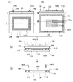
本実施の形態では、本発明の一態様の作製方法を用いて図1に示す封止体161を作製する方法を図2、図3を用いて説明する。
(Embodiment 1)
In this embodiment, a method for manufacturing the sealed
(緩衝層の形成)
まず、第2の基板300上に緩衝層140を形成する。第2の基板300はガラスを用いる。後述するレーザ光の照射を第2の基板300を介して行うため、第2の基板300はレーザ光を透過する基板であればよい。
(Formation of buffer layer)
First, the
緩衝層140となる膜は、酸化シリコン、窒化シリコンを用いることが出来る。酸化シリコン、窒化シリコンはプラズマCVD法を用いて成膜すればよい。後述するレーザ光の照射により第2の基板300に生じる引張り応力を緩和するため、緩衝層140は圧縮応力を有する層であればよい。
For the film to be the
緩衝層140は、フリットガラス層510を形成する領域に形成する(図2(A))。緩衝層140の形態は公知の技術を用いて形成すればよく、例えばフォトマスクを用いて形成したレジストマスクを用いてエッチングによって形成することができる。
The
(フリットガラスペーストの塗布)
つぎに、フリットガラスペースト500を緩衝層140と重なるように、第2の基板300上に塗布する(図2(B))。フリットガラスペースト500とは、粉末ガラスとバインダを含むものである。粉末ガラスは、例えば、酸化マグネシウム、酸化カルシウム、酸化バリウム、酸化リチウム、酸化ナトリウム、酸化カリウム、酸化ホウ素、酸化バナジウム、酸化亜鉛、酸化テルル、酸化アルミニウム、二酸化シリコン、酸化鉛、酸化スズ、酸化リン、酸化ルテニウム、酸化ロジウム、酸化鉄、酸化銅、酸化チタン、酸化タングステン、酸化ビスマス、酸化アンチモン、ホウ酸鉛ガラス、リン酸スズガラス、バナジン酸塩ガラスおよびホウケイ酸ガラスよりなる群から選択された1以上の化合物を含むことが望ましい。これに、例えば、有機溶媒で希釈した樹脂バインダを混ぜ、フリットガラスペーストとする。後述するレーザ光の照射でフリットガラス層510を加熱するため、レーザ光吸収材を添加したフリットガラスペーストを用いる。吸収材は使用するレーザ光の波長に合わせて最適なレーザ光吸収材を選択すればよい。
(Application of frit glass paste)
Next, a
フリットガラスペースト500の塗布方法は、ディスペンサ法、スクリーン印刷法またはインクジェット法を用いて形成することができる。この実施の形態では、表示装置などを封止するのに好適な長方形状としたが、閉曲線を成すものであれば、円状、楕円状などいかなる形状としてもよい。
As a method for applying the
(フリットガラスペーストの焼成)
フリットガラスペースト中のバインダを揮発させるため加熱を行う。具体的には温度は300〜450℃で加熱を行えばよい。当該加熱処理は、ランプやヒーターなどを利用して行なえばよい。当該加熱処理で、粉末ガラスを溶融し固化させることにより当該粉末ガラスを融合させ、フリットガラス層510とすることができる。この焼成の段階でフリットガラス層510は、第2の基板300上に切れ目のない閉曲線になるように形成する(図2(C))。気密性の優れた封止体を形成するためである。
(Baking of frit glass paste)
Heating is performed to volatilize the binder in the frit glass paste. Specifically, the heating may be performed at a temperature of 300 to 450 ° C. The heat treatment may be performed using a lamp, a heater, or the like. By the heat treatment, the powder glass is melted and solidified to fuse the powder glass, whereby the
(レーザ光の照射)
次に、第2の基板300上のフリットガラス層510と第1の基板130を密着させ、フリットガラス層510にレーザ光800を照射する(図3)。その結果、溶融したフリットガラス層510を介して、第2の基板300と第1の基板130が溶着する。レーザ光800の照射は第2の基板300を介してフリットガラス層510に行う。フリットガラス層510の表面でレーザ光は散乱しないので、フリットガラス層510が充分に溶融する。そのため、フリットガラス層510と第1の基板130が溶着して気密性の高い封止体を得ることが出来る。レーザ光の照射に用いるレーザの波長は750〜1200nmを用いることが出来る。800nmの半導体レーザが望ましい。
(Laser irradiation)
Next, the
フリットガラス層が直接設けられた基板にレーザ光を照射すると、基板とフリットガラス層が接する部分が、局所的に急速昇温された後、急冷される。そのため基板に局所的に大きな引張応力が発生して、基板とフリットガラス層にクラックが発生する場合がある。しかし、本実施の形態の第2の基板300には緩衝層140が設けられているため、レーザ光800が照射されたフリットガラス層510から生じる引張り応力を緩和して、第2の基板300のクラックの発生を抑制することができる。そのため、気密性の優れた封止体を作製することが出来る。
When the substrate on which the frit glass layer is directly provided is irradiated with laser light, a portion where the substrate and the frit glass layer are in contact with each other is rapidly heated locally and then rapidly cooled. Therefore, a large tensile stress is locally generated on the substrate, and a crack may be generated on the substrate and the frit glass layer. However, since the
以上の工程により、図1に示す封止体161を作製することができる。
Through the above steps, the sealing
以上のように、本実施の形態で示す封止体161の作製方法を用いると、緩衝層140が、レーザ光800の照射によって生じた第2の基板300の応力を緩和して、第2の基板300のクラックの発生を抑制する。その結果、気密性の高い封止体161を作製することができる。
As described above, when the method for manufacturing the sealing
また、本実施の形態で示す封止体161の作製方法は、第2の基板300を介してレーザ光800の照射を行っているため、フリットガラス層510の表面でレーザ光800が散乱しないで、フリットガラス層510が充分に溶融する。そのため、気密性の優れた封止体161を作製することができる。
Further, in the manufacturing method of the sealing
(実施の形態2)
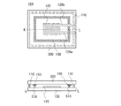
本実施の形態では、本発明の一態様の作製方法を用いて図4に示す封止体162を作製する方法を図5、図6を用いて説明する。
(Embodiment 2)
In this embodiment, a method for manufacturing the sealed
(緩衝層の形成)
まず、第2の基板300上に緩衝層150を成膜する。第2の基板300はガラスを用いる。後述するレーザ光の照射を第2の基板300を介して行うため、第2の基板300はレーザ光を透過する基板であればよい。
(Formation of buffer layer)
First, the
緩衝層150は、フリットガラス層510を形成する領域に形成する(図5)。緩衝層150の形態は公知の技術を用いて形成すればよく、例えばフォトマスクを用いて形成したレジストマスクを用いてエッチングによって形成することができる。
The
緩衝層150となる膜は、レーザ光を吸収して、ガラスの融点より高い融点の物質で形成することが出来る。具体的にはシリコン、DLC(ダイヤモンドライクカーボン)の絶縁物、タングステン、タンタル、鉄等の金属で形成することが出来る。シリコン、DLC(ダイヤモンドライクカーボン)はプラズマCVD法、メタルはスパッタリング法で形成することができる。
The film serving as the
後述するレーザ光の照射により第2の基板300に生じる引張り応力を緩和するため、シリコン、DLC(ダイヤモンドライクカーボン)等の絶縁物は、圧縮応力を有することが好ましい。
In order to relieve a tensile stress generated in the
または、シリコン、DLC(ダイヤモンドライクカーボン)の代わりに、緩衝層150は、タングステン、タンタル、鉄等の金属で延性を有する層であっても良い。フリットガラス層より高い融点をもつ金属は、レーザ光照射による発熱でフリットガラス層が溶融する前に金属が溶融しないため、フリットガラス層に熱を効率よく伝えることが出来る。
Alternatively, instead of silicon and DLC (diamond-like carbon), the
(フリットガラスペーストの塗布)
つぎに、第2の基板300上で緩衝層150と重なるように、フリットガラスペースト500を塗布する(図5)。本実施の形態ではレーザ吸収材を含まないフリットガラスペーストを用いる。その他のフリットガラスペーストの材料構成、塗布方法は、実施の形態1を参酌することが出来る。
(Application of frit glass paste)
Next, a
(フリットガラスペーストの焼成)
フリットガラスペースト500を焼成してフリットガラス層510を形成する工程は、実施の形態1を参酌することが出来る。この焼成の段階でフリットガラス層510は、第2の基板300上に切れ目のない閉曲線になるように形成する(図5)。気密性の優れた封止体を形成するためである。
(Baking of frit glass paste)
Embodiment 1 can be referred to for the step of baking the
(レーザ光の照射)
次に、第2の基板300上のフリットガラス層510と第1の基板130を密着させ、レーザ光の照射する(図6)。レーザ光800の照射は第2の基板300を介して緩衝層150に行う。緩衝層150がレーザ光800を吸収し、緩衝層150から熱伝導した熱がフリットガラス層510を溶融させ、フリットガラス層510と第1の基板を溶着させ、フリットガラス層510と第1の基板130と第2の基板300とで閉空間を形成する。緩衝層がなくフリットガラス層にレーザ光を吸収させる場合、フリットガラス層は膜厚が一定ではなく表面形状も凹凸を有するので、レーザ光が散乱する場合がある。一方、レーザ光を吸収する緩衝層150は、第2の基板300に膜厚が一定の薄膜として形成され、表面形状も凹凸がないため、レーザ光が散乱されにくくフリットガラス層510より効率よくレーザ光を吸収する。そのため、フリットガラス層に直接レーザ光を照射する場合より、低いエネルギーのレーザ光で溶着することが出来る。特に緩衝層150にタングステン、タンタル、鉄の金属を用いた場合、レーザ光を吸収しやすいため、フリットガラス層510に直接レーザ光を照射する場合より、低いレーザ光の照射エネルギーで溶着することが出来る。レーザ光の照射に用いるレーザ光の波長は750〜1200nmを用いることが出来る。具体的には800nmの半導体レーザが望ましい。
(Laser irradiation)
Next, the
フリットガラス層が直接設けられた基板にレーザ光を照射すると、基板にフリットガラス層が接する部分が、局所的に急速昇温・急冷される。そのため基板に局所的に大きな引張応力が発生して、基板とフリットガラス層にクラックが発生する場合がある。しかし、圧縮応力を有する層を緩衝層150に用いれば、第2の基板300に生じた引張り応力を緩和することができるので、第2の基板300のクラックの発生を抑制することができる。
When the substrate on which the frit glass layer is directly provided is irradiated with laser light, the portion where the frit glass layer is in contact with the substrate is rapidly heated and cooled locally. Therefore, a large tensile stress is locally generated on the substrate, and a crack may be generated on the substrate and the frit glass layer. However, if a layer having a compressive stress is used for the
また、レーザ光の照射により第2の基板300に生じた引張応力は、延性を有する金属を緩衝層150に用いることより緩和することができるので、第2の基板300のクラックの発生を抑制することができる。
Further, since the tensile stress generated in the
レーザ光を吸収する緩衝層150は、第2の基板300に平坦な薄膜として形成されているため、レーザ光が散乱されにくい。そのため、フリットガラス層が直接設けられた基板にレーザ光を照射する場合より、低いエネルギーのレーザ光で溶着することが出来る。
Since the
また、緩衝層150にフリットガラス層より高い融点を有する金属を用いた場合、金属の熱伝導率は絶縁物より高いため、レーザ光を吸収して発熱した熱をフリットガラス層に絶縁物より効率よく熱を伝えることが出来る。そのため、低いレーザ光の照射エネルギーで溶着することが出来る。
Further, when a metal having a melting point higher than that of the frit glass layer is used for the
レーザ光を吸収する緩衝層150を用いると、フリットガラスペースト500にレーザ吸収材を添加しなくてもよい。よって、フリットガラスペーストの材料費を抑制することができる。
When the
なお、本発明の一態様の封止体の作製方法は、フリットガラスペースト500を用いた場合に限られず、極めて薄い帯状のガラス薄膜を用いた場合にも適用することが出来る。例えば、フリットガラス層510に代えて厚さが100nm以上500μm以下、好ましくは100nm以上100μm以下の帯状のガラス薄膜を用い、緩衝層150に対してレーザ光を照射することにより、間接的に加熱して当該ガラス薄膜を溶融させ、当該ガラス薄膜と第1の基板130を溶着させ、当該ガラス薄膜と第1の基板130と第2の基板300とで閉空間を形成する。このような帯状のガラス薄膜を用いると、フリットガラスペースト500の仮焼成が不要であるため、工程を簡略化できる。
Note that the method for manufacturing a sealed body of one embodiment of the present invention is not limited to the case where the
以上の工程により、図4に示す封止体162を作製することができる。
Through the above steps, the sealing
以上のように、本実施の形態で示す封止体162の作製方法を用いると、圧縮応力を有する層を緩衝層150に用いれば、レーザ光の照射によって生じた第2の基板300の応力を緩和して、第2の基板300のクラックの発生を抑制する。その結果、気密性の高い封止体162を作製することができる。
As described above, when the method for manufacturing the sealing
また、延性を有する金属を緩衝層150に用いれば、レーザ光の照射によって生じた第2の基板300の応力を緩和して、第2の基板300のクラックの発生を抑制する。その結果、気密性の高い封止体162を作製することができる。
In addition, when a metal having ductility is used for the
また、本実施の形態で示す封止体162の作製方法は、緩衝層150にレーザ光800を照射してフリットガラス層510を溶融している。緩衝層150が第2の基板300に平坦な薄膜として形成されているため、レーザ光800が散乱されにくい。そのため、フリットガラス層510に直接レーザ光を照射する場合より、低いエネルギーのレーザ光で溶着することが出来る。また、緩衝層150に金属を用いた場合、金属の熱伝導率は絶縁物より高いため、レーザ光800を吸収して発熱した熱をフリットガラス層510に絶縁物より効率よく熱を伝えることが出来る。そのため、低いレーザ光の照射エネルギーで溶着することが出来る。また、フリットガラスペースト500にレーザ吸収材を添加しなくてもよいため、フリットガラスペースト500の材料費を低減できる。
In the manufacturing method of the sealing
(実施の形態3)
本実施の形態では、図7に示す発光装置163の作製方法の一形態を、図8、図9を用いて説明する。本実施の形態では、発光素子の一態様として有機EL素子を用いた場合について説明する。
(Embodiment 3)
In this embodiment, one embodiment of a method for manufacturing the light-emitting
(緩衝層の形成)
まず、第2の基板300上に緩衝層140を成膜する。第2の基板300はガラスを用いる。後述するレーザ光の照射を第2の基板300を介して行うため、第2の基板300はレーザ光を透過する基板であればよい。緩衝層140は、フリットガラス層510を形成する領域に形成する。第2の基板300と第1の基板130を貼り合わせた状態で、緩衝層140は、有機EL素子125を囲むように、形成すればよい。緩衝層140のパターン形成は公知の技術を用いればよく、エッチングによって形成することができる。
(Formation of buffer layer)
First, the
緩衝層140には、酸化シリコン、窒化シリコンを用いることが出来る。酸化シリコン、窒化シリコンはプラズマCVD法を用いて成膜すればよい。後述するレーザ光の照射により第2の基板300に生じる引張り応力を緩和するため、緩衝層140は圧縮応力を有する層であればよい。
For the
(フリットガラスペーストの塗布)
つぎに、第2の基板300上で緩衝層140と重なるように、フリットガラスペースト500を塗布する。本実施の形態では、実施の形態1を参酌することが出来る。
(Application of frit glass paste)
Next, a
(フリットガラスペーストの焼成)
フリットガラスペースト500を焼成してフリットガラス層510を形成する工程は、実施の形態1を参酌することが出来る。この焼成の段階でフリットガラス層510は、第2の基板300上に閉曲線になるように形成する。気密性の高い封止体で有機EL素子125を封止するためである。
(Baking of frit glass paste)
Embodiment 1 can be referred to for the step of baking the
(有機EL素子の形成)
まず、図8(A)に示すように、第1の基板130上に有機EL素子125を設ける。有機EL素子125は、例えば、第1の基板130に近いほうから陽極、発光層、陰極の順に積まれた積層構造を有する。陽極と陰極を入れ替えてもよい。これらの他に別の層を追加で設けても構わない。陽極からは端子126aが、陰極からは端子126bがそれぞれ出ており、これらを外部電源に接続することで、有機EL素子125に電力を供給できる。
(Formation of organic EL elements)
First, as illustrated in FIG. 8A, the
(シール材の形成)
次に、図8(B)に示すように、有機EL素子125を囲むように、かつフリットガラス層510と貼り合わせる領域と重ならないように、シール材110を形成する。シール材110で、第1の基板130と第2の基板300を貼り合わせる理由は、フリットガラス層510に粘着性がなく、第1の基板130と第2の基板の位置合わせが困難であるためである。シール材110は、紫外線硬化樹脂、エポキシ樹脂などを用い、ディスペンサ法、スクリーン印刷法で塗布すればよい。該シール材110は第1の基板130上で閉曲線に形成する。該シール材110においても外気の侵入を防ぐためである。なお、シール材110の閉曲線は、フリットガラス層510が形成される領域の内側、または外側のどちらでもよい。
(Formation of sealing material)
Next, as illustrated in FIG. 8B, a
(シール材の硬化)
次に、シール材110を塗布した有機EL素子125を有する第1の基板130と、フリットガラス層510を形成した第2の基板300を貼り合わせる。紫外線硬化樹脂を用いる場合、有機EL素子125に紫外線が当たらないように遮光マスク600で有機EL素子125を遮光し、紫外線700を照射してシール材110を硬化させ、第1の基板130と第2の基板を接着させる(図9(C))。
(Curing sealant)
Next, the
(レーザ光の照射)
次に、フリットガラス層510にレーザ光を照射して、フリットガラス層510を溶融させ、フリットガラス層510と第1の基板130を溶着する(図9(D))。レーザ光の照射は第2の基板300を介してフリットガラス層510に行う。フリットガラス層510の表面でレーザ光が散乱されないので、フリットガラス層510を充分に溶融することができる。レーザ光の照射に用いるレーザの波長は750〜1200nmを用いることが出来る。具体的には800nmの半導体レーザが望ましい。
(Laser irradiation)
Next, the
フリットガラス層が直接設けられた基板にレーザ光を照射すると、基板にフリットガラス層が接する部分が、局所的に急速昇温・急冷される。そのため基板に局所的に大きな引張応力が発生して、基板とフリットガラス層にクラックが発生する場合がある。しかし、緩衝層140が、第2の基板300に生じた引張り応力を緩和して、第2の基板300のクラックの発生を抑制することができる。
When the substrate on which the frit glass layer is directly provided is irradiated with laser light, the portion where the frit glass layer is in contact with the substrate is rapidly heated and cooled locally. Therefore, a large tensile stress is locally generated on the substrate, and a crack may be generated on the substrate and the frit glass layer. However, the
以上の工程により、図7に示す発光装置163を作製することができる。
Through the above steps, the light-emitting
以上のように、本実施の形態で示す発光装置163の作製方法を用いると、第2の基板300においてクラックの発生を抑制することができる。緩衝層140が、レーザ光の照射によって生じた第2の基板300の応力を緩和して、第2の基板300のクラックの発生を抑制するためである。フリットガラス層510は気密性を有するので、外部から水分、大気成分の侵入を抑制できる。その結果、気密性の高い封止により信頼性の優れた発光装置163を作製することができる。
As described above, when the method for manufacturing the light-emitting
また、本実施の形態で示す発光装置163の作製方法は、第2の基板300を介してレーザ光の照射を行っているため、フリットガラス層510の表面でレーザ光が散乱しないので、フリットガラス層510が充分に溶融する。そのため、フリットガラス層510と第1の基板130の溶着が不完全になることを防止することが出来る。その結果、気密性の高い封止体により信頼性の高い発光装置163を作製することができる。
Further, in the method for manufacturing the light-emitting
(実施の形態4)
本実施の形態では、図10に示す発光装置164の作製方法の一形態を、図11を用いて説明する。
(Embodiment 4)
In this embodiment, one embodiment of a method for manufacturing the light-emitting
(緩衝層の形成)
まず、第2の基板300上に緩衝層150を成膜する。第2の基板300はガラスを用いる。後述するレーザ光の照射を第2の基板300を介して行うため、第2の基板300はレーザ光を透過する基板であればよい。緩衝層150は、フリットガラス層510を形成する領域に形成する(図11(C))。緩衝層150の形態は公知の技術を用いて形成すればよく、例えばフォトマスクを用いて形成したレジストマスクを用いてエッチングによって形成することができる。後述するように第2の基板300は、発光素子を形成する第1の基板130とフリットガラス層510を介して貼り合わせる。そのため貼り合わせた状態で発光素子を囲むように、緩衝層150を第2の基板300上に形成する。
(Formation of buffer layer)
First, the
緩衝層150の構成、形成については、実施の形態2を参酌することが出来る。
(フリットガラスペーストの塗布)
つぎに、第2の基板300上で緩衝層150と重なるように、フリットガラスペースト500を塗布する。本実施の形態ではレーザ光吸収材を含まないフリットガラスペーストを用いる。その他のフリットガラスペーストの材料構成、塗布方法は、実施の形態1を参酌することが出来る。
(Application of frit glass paste)
Next, a
(フリットガラスペーストの焼成)
フリットガラスペースト500を焼成してフリットガラス層510を形成する工程は、実施の形態1を参酌することが出来る。この焼成の段階でフリットガラス層510は、第2の基板300上に切れ目のない閉曲線になるように形成する。気密性の高い封止体を形成するためである。
(Baking of frit glass paste)
Embodiment 1 can be referred to for the step of baking the
(有機EL素子、シール材の形成)
第1の基板130上に有機EL素子125を設ける工程、第1の基板130上にシール材110を形成する工程および、シール材110を硬化させ第1の基板130と第2の基板300を貼り合わせる工程は、実施の形態3を参酌することが出来る。
(Formation of organic EL elements and sealing materials)
The step of providing the
(レーザ光の照射)
次に、第2の基板300上のフリットガラス層510と第1の基板130を密着させ、レーザ光800を照射する(図11(D))。レーザ光800の照射は第2の基板300を介して緩衝層150に行う。緩衝層150がレーザ光800を吸収し、緩衝層150から熱伝導した熱がフリットガラス層510を溶融させ、フリットガラス層510と第1の基板を溶着させ、フリットガラス層510と第1の基板130と第2の基板300とで閉空間を形成する。レーザ光を吸収する緩衝層150は、第2の基板に平坦な薄膜として形成されているため、レーザ光が散乱されにくい。そのためレーザ光が散乱されにくいので、緩衝層150は、フリットガラス層510に比べレーザ光を効率よく吸収する。よって、フリットガラス層510に直接レーザ光を照射する場合より、低いエネルギーのレーザ光で溶着することが出来る。特に緩衝層150にタングステン、タンタル、鉄の金属を用いた場合、レーザ光を吸収しやすいため、フリットガラス層510に直接レーザ光を照射する場合より、低いレーザ光の照射エネルギーで溶着することが出来る。レーザ光の照射に用いるレーザ光の波長は750〜1200nmを用いることが出来る。具体的には800nmの半導体レーザが望ましい。
(Laser irradiation)
Next, the
フリットガラス層が直接設けられた基板にレーザ光を照射すると、基板にフリットガラス層が接する部分が、局所的に急速昇温・急冷される。そのため基板に局所的に大きな引張応力が発生して、基板とフリットガラス層にクラックが発生する場合がある。しかし、圧縮応力を有する層を緩衝層150に用いれば、第2の基板300に生じた引張り応力を緩和することができるので、第2の基板300のクラックの発生を抑制することができる。
When the substrate on which the frit glass layer is directly provided is irradiated with laser light, the portion where the frit glass layer is in contact with the substrate is rapidly heated and cooled locally. Therefore, a large tensile stress is locally generated on the substrate, and a crack may be generated on the substrate and the frit glass layer. However, if a layer having a compressive stress is used for the
また、レーザ光の照射により第2の基板300に生じた引張応力は、延性を有する金属を緩衝層150に用いると、第2の基板300に生じた引張り応力を緩和することができるので、第2の基板300のクラックの発生を抑制することができる。
In addition, the tensile stress generated in the
緩衝層がなくフリットガラス層にレーザ光を吸収させる場合、フリットガラス層は膜厚が一定ではなく表面形状も凹凸を有するので、レーザ光が散乱する場合がある。一方、レーザ光を吸収する緩衝層150は、第2の基板300に膜厚が一定の薄膜として形成され、表面形状も凹凸がないため、レーザ光が散乱されにくくフリットガラス層510より効率よくレーザ光を吸収する。そのため、フリットガラス層に直接レーザ光を照射する場合より、低いエネルギーのレーザ光で溶着することが出来る。
When there is no buffer layer and the frit glass layer absorbs laser light, the frit glass layer has a constant film thickness and has irregularities on the surface, so that the laser light may be scattered. On the other hand, the
また、緩衝層にフリットガラス層より高い融点を有する金属を用いた場合、金属の熱伝導率は絶縁物より高いため、レーザ光を吸収して発熱した熱をフリットガラス層に絶縁物より効率よく熱を伝えることが出来る。そのため、低いレーザ光の照射エネルギーで溶着することが出来る。 In addition, when a metal having a higher melting point than the frit glass layer is used for the buffer layer, the heat conductivity of the metal is higher than that of the insulator, so that the heat generated by absorbing the laser light is more efficiently transferred to the frit glass layer than the insulator. Can convey heat. Therefore, welding can be performed with low laser light irradiation energy.
レーザ光を吸収する緩衝層150を用いると、フリットガラスペーストにレーザ吸収材を添加しなくてもよい。よって、フリットガラスペーストの材料費を抑制することができる。
When the
なお、本発明の一態様の封止体の作製方法は、フリットガラスペースト500を用いた場合に限られず、極めて薄い帯状のガラス薄膜を用いた場合にも適用することが出来る。例えば、フリットガラス層510に代えて厚さが100nm以上500μm以下、好ましくは100nm以上100μm以下の帯状のガラス薄膜を用い、緩衝層150に対してレーザ照射することにより、間接的に加熱して当該ガラス薄膜を溶融させ、当該ガラス薄膜と第1の基板130を溶着させ、当該ガラス薄膜と第1の基板130と第2の基板300とで閉空間を形成する。このような帯状のガラス薄膜を用いると、フリットガラスペースト500の仮焼成が不要であるため、工程を簡略化できる。
Note that the method for manufacturing a sealed body of one embodiment of the present invention is not limited to the case where the
以上の工程により、図10に示す発光装置164を作製することができる。
Through the above steps, the light-emitting
以上のように、本実施の形態で示す発光装置164の作製方法を用いると、圧縮応力を有する層を緩衝層150に用いれば、レーザ光の照射によって生じた第2の基板300の応力を緩和して、第2の基板300のクラックの発生を抑制する。その結果、気密性の高い発光装置164を作製することができる。
As described above, when the method for manufacturing the light-emitting
また、延性を有する金属を緩衝層150に用いれば、レーザ光の照射によって生じた第2の基板300の応力を緩和して、第2の基板300のクラックの発生を抑制する。その結果、気密性の高い発光装置164を作製することができる。
In addition, when a metal having ductility is used for the
また、本実施の形態で示す発光装置164の作製方法は、緩衝層150にレーザ光800を照射してフリットガラス層510を溶融している。緩衝層150が第2の基板に平坦な薄膜として形成されているため、レーザ光が散乱されにくい。そのため、フリットガラス層510にレーザ光を直接照射する場合より、低いエネルギーのレーザ光で溶着することが出来る。また、緩衝層150に金属を用いた場合、金属の熱伝導率は絶縁物より高いため、レーザ光800を吸収して発熱した熱をフリットガラス層510に絶縁物より効率よく熱を伝えることが出来る。そのため、低いレーザ光の照射エネルギーで溶着することが出来る。また、フリットガラスペースト500にレーザ吸収材を添加しなくてもよいため、フリットガラスペースト500の材料費を低減できる。
In the manufacturing method of the light-emitting
(実施の形態5)
実施の形態3および4において説明した有機EL素子125に適用可能な構成の一態様について、図12(A)を用いて説明する。なお、本実施の形態では第1の電極102と第2の電極104に挟持された有機EL層103を有する発光素子の構成について詳細に説明する。また、第1の電極102には端子126bが接続され、第2の電極104には端子126aが接続される。
(Embodiment 5)
One mode of a structure that can be applied to the
発光素子は、一対の電極(第1の電極102及び第2の電極104)と、当該一対の電極間に挟まれた有機EL層103を有する。また、本実施の形態で説明する発光素子は、ガラス基板100上に設けられている。
The light-emitting element includes a pair of electrodes (a
ガラス基板100は、発光素子の支持体として用いられる。ガラス基板100としては、長方形の板状のものは勿論、曲面を有するものなど様々な形状のものを用いることができる。
The
第1の電極102及び第2の電極104は、一方が陽極として機能し、他方が陰極として機能する。本実施の形態においては、第1の電極102を陽極として用い、第2の電極104を陰極として用いるものとして説明するが、本発明はこの構成に限定されるものではない。
One of the
陽極として用いる材料は、仕事関数の大きい(具体的には4.0eV以上)金属、合金、導電性化合物、またはこれらの混合物などが好ましい。具体的には、酸化インジウム−酸化スズ(ITO:Indium Tin Oxide)、シリコン若しくは酸化シリコンを含有した酸化インジウム−酸化スズ、酸化インジウム−酸化亜鉛(Indium Zinc Oxide)、酸化タングステン及び酸化亜鉛を含有した酸化インジウム(IWZO)等が挙げられる。この他、金(Au)、白金(Pt)、ニッケル(Ni)、タングステン(W)、クロム(Cr)、モリブデン(Mo)、鉄(Fe)、コバルト(Co)、銅(Cu)、パラジウム(Pd)、または金属材料の窒化物(例えば、窒化チタン)等が挙げられる。 The material used as the anode is preferably a metal, an alloy, a conductive compound, or a mixture thereof having a high work function (specifically, 4.0 eV or more). Specifically, indium oxide-tin oxide (ITO), indium oxide-tin oxide containing silicon or silicon oxide, indium zinc-oxide (Indium Zinc Oxide), tungsten oxide and zinc oxide were contained. Examples thereof include indium oxide (IWZO). In addition, gold (Au), platinum (Pt), nickel (Ni), tungsten (W), chromium (Cr), molybdenum (Mo), iron (Fe), cobalt (Co), copper (Cu), palladium ( Pd), or a nitride of a metal material (for example, titanium nitride).
陰極として用いる材料は、仕事関数の小さい(具体的には3.8eV以下)金属、合金、電気伝導性化合物、またはこれらの混合物などが好ましい。具体的には、元素周期表の第1族または第2族に属する元素、すなわちリチウム(Li)やセシウム(Cs)等のアルカリ金属、カルシウム(Ca)、ストロンチウム(Sr)等のアルカリ土類金属、マグネシウム(Mg)が挙げられる。また、アルカリ金属またはアルカリ土類金属を含む合金(例えばMgAg、AlLi)を用いることもできる。また、ユウロピウム(Eu)、イッテルビウム(Yb)などの希土類金属、または希土類金属を含む合金を用いることもできる。また、有機EL層103の一部として、第2の電極104に接する電子注入層を設ける場合、仕事関数の大小に関わらず、Al、Ag、ITOなどの様々な導電性材料を第2の電極104として用いることができる。これら導電性材料は、スパッタリング法やインクジェット法、スピンコート法等を用いて薄膜とすることが可能である。
The material used as the cathode is preferably a metal, an alloy, an electrically conductive compound, or a mixture thereof having a low work function (specifically, 3.8 eV or less). Specifically, elements belonging to Group 1 or
有機EL層103は、単層構造で構成されることも可能であるが、通常積層構造から構成される。有機EL層103の積層構造については特に限定されず、電子輸送性の高い物質を含む層(電子輸送層)または正孔輸送性の高い物質を含む層(正孔輸送層)、電子注入性の高い物質を含む層(電子注入層)、正孔注入性の高い物質を含む層(正孔注入層)、バイポーラ性(電子及び正孔の輸送性の高い物質)の物質を含む層、発光材料を含む層(発光層)などを適宜組み合わせて構成すればよい。例えば、正孔注入層、正孔輸送層、発光層、電子輸送層、電子注入層等を適宜組み合わせて構成することができる。図12(A)においては、第1の電極102の上に形成された有機EL層103として、正孔注入層111、正孔輸送層112、発光層113、電子輸送層114が順に積層された構造を示している。
The
発光素子は、第1の電極102と第2の電極104との間に生じた電位差により電流が流れ、発光性の高い物質を含む層である発光層113において正孔と電子とが再結合し、発光するものである。つまり発光層113に発光領域が形成されるような構成となっている。
In the light-emitting element, current flows due to a potential difference generated between the
発光は、第1の電極102または第2の電極104のいずれか一方または両方を通って外部に取り出される。従って、第1の電極102または第2の電極104のいずれか一方または両方は、透光性を有する電極で成る。第1の電極102のみが透光性を有する電極である場合、発光は第1の電極102を通ってガラス基板100側から取り出される。また、第2の電極104のみが透光性を有する電極である場合、発光は第2の電極104を通って基板と逆側から取り出される。第1の電極102および第2の電極104がいずれも透光性を有する電極である場合、発光は第1の電極102および第2の電極104を通って、ガラス基板100側と逆側の両方から取り出される。
Light emission is extracted outside through one or both of the
発光層113に接する正孔輸送層112や電子輸送層114、特に発光層113における発光領域に近い方に接するキャリア(電子または正孔)輸送層は、発光層113で生成した励起子からのエネルギー移動を抑制するため、発光層を構成する発光材料、または発光層に含まれる発光中心物質よりも大きなエネルギーギャップを有する物質で構成することが好ましい。
The
正孔注入層111は、正孔注入性の高い物質を含み、第1の電極102から正孔輸送層112へ正孔の注入を補助する機能を有する。正孔注入層111には、第1の電極102と正孔輸送層112との間のイオン化ポテンシャルの差を緩和し、正孔が注入され易くなるものを選ぶ。正孔注入層111は、イオン化ポテンシャルを正孔輸送層112よりも小さく、第1の電極102よりも大きい物質が好ましい。正孔注入層111には、例えば、フタロシアニン(略称:H2Pc)や銅フタロシアニン(CuPc)等のフタロシアニン系の化合物、またはポリ(エチレンジオキシチオフェン)/ポリ(スチレンスルホン酸)水溶液(PEDOT/PSS)等の高分子を用いることができる。
The
正孔輸送層112は、正孔輸送性の高い物質を含む。正孔輸送性の高い物質とは、正孔の移動度が電子のそれよりも高いものを指し、電子の移動度に対する正孔の移動度の比(=正孔移動度/電子移動度)が100よりも大きいものを利用するのが好ましい。また、正孔輸送層112の正孔移動度は、1×10−6cm2/Vs以上とするのが好ましい。具体的には、4,4’−ビス[N−(1−ナフチル)−N−フェニルアミノ]ビフェニル(略称:NPB)、4,4’−ビス[N−(3−メチルフェニル)−N−フェニルアミノ]ビフェニル(略称:TPD)、4,4’,4’’−トリス(N,N−ジフェニルアミノ)トリフェニルアミン(略称:TDATA)、4,4’,4’’−トリス[N−(3−メチルフェニル)−N−フェニルアミノ]トリフェニルアミン(略称:MTDATA)、4,4’−ビス{N−[4−(N,N−ジ−m−トリルアミノ)フェニル]−N−フェニルアミノ}ビフェニル(略称:DNTPD)、1,3,5−トリス[N,N−ジ(m−トリル)アミノ]ベンゼン(略称:m−MTDAB)、4,4’,4’’−トリス(N−カルバゾリル)トリフェニルアミン(略称:TCTA)、フタロシアニン(略称:H2Pc)、銅フタロシアニン(略称:CuPc)、バナジルフタロシアニン(略称:VOPc)などを利用できる。また、正孔輸送層112は、単層構造としてもよいし、積層構造としてもよい。
The
電子輸送層114は、電子輸送性の高い物質を含む。電子輸送性の高い物質とは、電子の移動度が正孔のそれよりも高いものを指し、正孔の移動度に対する電子の移動度の比(=電子移動度/正孔移動度)が100よりも大きいものを利用するのが好ましい。また、電子輸送層114の電子移動度は、1×10−6cm2/Vs以上とするのが好ましい。具体的には、キノリン骨格を有する金属錯体、ベンゾキノリン骨格を有する金属錯体、オキサゾール系配位子を有する金属錯体、チアゾール系配位子を有する金属錯体を利用できる。キノリン骨格を有する金属錯体の具体例としては、トリス(8−キノリノラト)アルミニウム(略称:Alq)、トリス(4−メチル−8−キノリノラト)アルミニウム(略称:Almq3)、ビス(2−メチル−8−キノリノラト)(4−フェニルフェノラト)アルミニウム(略称:BAlq)が挙げられる。また、ベンゾキノリン骨格を有する金属錯体の具体例としては、ビス(10−ヒドロキシベンゾ[h]キノリナト)ベリリウム(略称:BeBq2)が挙げられる。また、オキサゾール系配位子を有する金属錯体の具体例としては、ビス[2−(2−ヒドロキシフェニル)ベンズオキサゾラト]亜鉛(略称:Zn(BOX)2)が挙げられる。また、チアゾール系配位子を有する金属錯体の具体例としては、ビス[2−(2−ヒドロキシフェニル)ベンゾチアゾラト]亜鉛(略称:Zn(BTZ)2)が挙げられる。また、金属錯体以外にも、2−(4−ビフェニリル)−5−(4−tert−ブチルフェニル)−1,3,4−オキサジアゾール(略称:PBD)や、1,3−ビス[5−(p−tert−ブチルフェニル)−1,3,4−オキサジアゾール−2−イル]ベンゼン(略称:OXD−7)、3−(4−ビフェニリル)−4−フェニル−5−(4−tert−ブチルフェニル)−1,2,4−トリアゾール(略称:TAZ 01)、バソフェナントロリン(略称:BPhen)、バソキュプロイン(略称:BCP)なども用いることができる。具体例を挙げた上述の物質は、主に10−6cm2/Vs以上の電子移動度を有する物質である。なお、正孔よりも電子の輸送性の高い物質であれば、これら以外の物質を電子輸送層114として用いてもよい。また、電子輸送層114は、単層構造としてもよいし、積層構造としてもよい。 The electron transport layer 114 includes a substance having a high electron transport property. A substance having a high electron transporting property refers to a substance having electron mobility higher than that of holes, and the ratio of electron mobility to hole mobility (= electron mobility / hole mobility) is 100. It is preferable to use a larger one. The electron mobility of the electron transport layer 114 is preferably 1 × 10 −6 cm 2 / Vs or higher. Specifically, a metal complex having a quinoline skeleton, a metal complex having a benzoquinoline skeleton, a metal complex having an oxazole ligand, and a metal complex having a thiazole ligand can be used. Specific examples of the metal complex having a quinoline skeleton include tris (8-quinolinolato) aluminum (abbreviation: Alq), tris (4-methyl-8-quinolinolato) aluminum (abbreviation: Almq 3 ), and bis (2-methyl-8). -Quinolinolato) (4-phenylphenolato) aluminum (abbreviation: BAlq). As a specific example of the metal complex having a benzoquinoline skeleton, bis (10-hydroxybenzo [h] quinolinato) beryllium (abbreviation: BeBq 2 ) can be given. As a specific example of a metal complex having an oxazole-based ligand, bis [2- (2-hydroxyphenyl) benzoxazolate] zinc (abbreviation: Zn (BOX) 2 ) can be given. As a specific example of a metal complex having a thiazole-based ligand, bis [2- (2-hydroxyphenyl) benzothiazolate] zinc (abbreviation: Zn (BTZ) 2 ) can be given. In addition to metal complexes, 2- (4-biphenylyl) -5- (4-tert-butylphenyl) -1,3,4-oxadiazole (abbreviation: PBD), 1,3-bis [5 -(P-tert-butylphenyl) -1,3,4-oxadiazol-2-yl] benzene (abbreviation: OXD-7), 3- (4-biphenylyl) -4-phenyl-5- (4- tert-Butylphenyl) -1,2,4-triazole (abbreviation: TAZ 01), bathophenanthroline (abbreviation: BPhen), bathocuproin (abbreviation: BCP), and the like can also be used. The above-described substances with specific examples are mainly substances having an electron mobility of 10 −6 cm 2 / Vs or more. Note that a substance other than these substances may be used for the electron-transport layer 114 as long as it has a property of transporting more electrons than holes. Further, the electron transport layer 114 may have a single-layer structure or a stacked structure.
また、発光層113と電子輸送層114との間に電子キャリアの移動を制御する層を設けてもよい。電子キャリアの移動を制御する層は、上述したような電子輸送性の高い材料に対して、電子トラップ性の高い物質を少量添加した層である。電子キャリアの移動を制御する層を設けることにより、電子キャリアの移動を抑制し、キャリアバランスを調節することが可能となる。このような構成は、発光層を電子が突き抜けてしまうことにより発生する問題(例えば素子寿命の低下)の抑制に大きな効果を発揮する。
Further, a layer for controlling the movement of electron carriers may be provided between the light-emitting
また、電子輸送層114と第2の電極104との間に、第2の電極104に接して電子注入層を設けてもよい。電子注入層としては、電子輸送性を有する物質からなる層中に、フッ化リチウム(LiF)、フッ化セシウム(CsF)、フッ化カルシウム(CaF2)などのようなアルカリ金属、アルカリ土類金属、またはそれらの化合物を含有させたものを用いればよい。具体例としては、Alq中にマグネシウム(Mg)を含有させたものを用いることができる。電子注入層を設けることにより、第2の電極104からの電子注入を効率良く行うことができる。
Further, an electron injection layer may be provided in contact with the
また、有機EL層103は、乾式法、湿式法を問わず、種々の方法を用いて形成できる。例えば、真空蒸着法、インクジェット法、またはスピンコート法を用いることができる。また、有機EL層103を積層構造とする場合、各層毎に異なる方法を用いて形成してもよいし、各層全てを同一の方法で形成してもよい。
The
また、第1の電極102、第2の電極104は、ゾル−ゲル法や液状の金属材料を用いた湿式法で形成してもよいし、スパッタリング法や真空蒸着法などの乾式法で形成してもよい。このような発光素子と本発明の一態様である封止体の作製方法を組み合わせることにより、信頼性の高い発光装置を作製することができる。
The
以上、本実施の形態に示す方法などは、他の実施の形態に示す方法などと適宜組み合わせて用いることができる。 As described above, the method described in this embodiment can be combined as appropriate with any of the methods described in the other embodiments.
(実施の形態6)
本実施の形態では、本発明の一態様の封止体作製方法により封止した、複数の発光ユニットを積層した構成を有する発光素子(以下、「タンデム型の発光素子」という)について、図12(B)を参照しながら説明する。タンデム型の発光素子は、第1の電極と第2の電極との間に、複数の発光ユニットを有する。発光ユニットとしては、先に示した有機EL層103と同様な構成を用いることができる。
(Embodiment 6)
In this embodiment, a light-emitting element having a structure in which a plurality of light-emitting units is stacked (hereinafter, referred to as a “tandem light-emitting element”) sealed by the sealing body manufacturing method of one embodiment of the present invention is described with reference to FIG. This will be described with reference to (B). A tandem light-emitting element includes a plurality of light-emitting units between a first electrode and a second electrode. As the light emitting unit, a structure similar to that of the
図12(B)において、第1の電極501と第2の電極502との間には、第1の発光ユニット511と第2の発光ユニット512が積層されている。第1の電極501と第2の電極502は、実施の形態5と同様なものを適用することができる。また、第1の発光ユニット511と第2の発光ユニット512は同じ構成であっても異なる構成であってもよく、各ユニットの構成は、それぞれ実施の形態5に示したものと同様なものを適用することができる。
In FIG. 12B, a first light-emitting
第1の発光ユニット511と第2の発光ユニット512との間には、電荷発生層513が設けられている。電荷発生層513は、有機化合物と金属酸化物の複合材料を含み、第1の電極501と第2の電極502に電圧を印加したときに、一方の側の発光ユニットに電子を注入し、他方の側の発光ユニットに正孔を注入する機能を有する。有機化合物と金属酸化物の複合材料は、キャリア注入性、キャリア輸送性に優れているため、低電圧駆動、低電流駆動を可能にする。
A
正孔輸送性の有機化合物には、正孔移動度が10−6cm2/Vs以上であるものを用いることが好ましい。具体的には、芳香族アミン化合物、カルバゾール化合物、芳香族炭化水素、高分子化合物、オリゴマー、デンドリマーなどが利用できる。また、それらと混ぜる金属酸化物には、元素周期表における第4族乃至第8族に属する金属の酸化物を用いればよく、具体的には、酸化バナジウム、酸化ニオブ、酸化タンタル、酸化クロム、酸化モリブデン、酸化タングステン、酸化マンガン、酸化レニウムが挙げられ、これらの金属酸化物は電子受容性が高いため、好ましい。特に、酸化モリブデンは大気中でも安定であり、吸湿性が低く、且つ扱いやすいため、特に好ましい。 As the hole-transporting organic compound, an organic compound having a hole mobility of 10 −6 cm 2 / Vs or higher is preferably used. Specifically, aromatic amine compounds, carbazole compounds, aromatic hydrocarbons, polymer compounds, oligomers, dendrimers, and the like can be used. Further, as the metal oxide mixed with them, an oxide of a metal belonging to Group 4 to Group 8 in the periodic table of elements may be used. Specifically, vanadium oxide, niobium oxide, tantalum oxide, chromium oxide, Examples thereof include molybdenum oxide, tungsten oxide, manganese oxide, and rhenium oxide, and these metal oxides are preferable because of their high electron accepting properties. Molybdenum oxide is particularly preferable because it is stable in the air, has a low hygroscopic property, and is easy to handle.
また、電荷発生層513は、単層構造でもよいし、積層構造でもよい。例えば、有機化合物と金属酸化物の複合材料を含む層と、電子供与性物質の中から選ばれた一の化合物、及び電子輸送性の高い化合物を含む層とを積層した構造としてもよいし、有機化合物と金属酸化物の複合材料を含む層と、透明導電膜とを積層した構造としてもよい。
The
本実施の形態では、2つの発光ユニットを有する発光素子について説明したが、本発明はこの構成に限定されるものではない。すなわち、タンデム型の発光素子は、3つ以上の発光ユニットを有していてもよい。この場合も、各発光ユニットの間には電荷発生層を設ける。例えば、第1のユニットと、それよりも長波長の発光(例えば、赤色の発光)を呈する第1の発光材料を用いて作製される第2のユニットと、第1のユニットよりも長波長、かつ第1の発光材料よりも短波長の発光(例えば、緑色の発光)を呈する第2の発光材料を用いて作製される第3のユニットとを有する発光素子を構成してもよい。これらの発光ユニットを用いることにより、白色の発光装置を得ることができる。 Although the light-emitting element having two light-emitting units has been described in this embodiment mode, the present invention is not limited to this structure. That is, the tandem light-emitting element may include three or more light-emitting units. Also in this case, a charge generation layer is provided between the light emitting units. For example, a first unit, a second unit manufactured using a first light-emitting material that emits light having a longer wavelength (for example, red light), and a longer wavelength than the first unit, In addition, a light-emitting element including a third unit manufactured using a second light-emitting material that emits light having a shorter wavelength than the first light-emitting material (for example, green light emission) may be configured. By using these light emitting units, a white light emitting device can be obtained.
本実施の形態に係るタンデム型の発光素子は、一対の電極間に複数の発光ユニットを電荷発生層で仕切って配置するため、電流密度を低く保ったまま高輝度の発光を可能にする。電流密度を低くできるため、高輝度でも長寿命な発光素子とすることができる。このような発光素子と本発明の一態様である封止体の作製方法を組み合わせることにより、信頼性の高い発光装置を作製することができる。 In the tandem light-emitting element according to this embodiment, a plurality of light-emitting units are partitioned by a charge generation layer between a pair of electrodes, and thus high-luminance light emission is possible while keeping a current density low. Since the current density can be reduced, a light-emitting element with high luminance and a long lifetime can be obtained. A highly reliable light-emitting device can be manufactured by combining such a light-emitting element and a manufacturing method of a sealed structure which is one embodiment of the present invention.
以上、本実施の形態に示す方法などは、他の実施の形態に示す方法などと適宜組み合わせて用いることができる。 As described above, the method described in this embodiment can be combined as appropriate with any of the methods described in the other embodiments.
(実施の形態7)
(パッシブマトリクス型の発光装置、及びアクティブマトリクス型の発光装置の説明)
本実施の形態では、本発明の一態様である封止体の作製方法で封止したパッシブマトリクス型の発光装置、及びアクティブマトリクス型の発光装置について説明する。
(Embodiment 7)
(Description of passive matrix light-emitting device and active matrix light-emitting device)
In this embodiment, a passive matrix light-emitting device and an active matrix light-emitting device which are sealed with a manufacturing method of a sealing body which is one embodiment of the present invention will be described.
図13、図14にパッシブマトリクス型の発光装置の例を示す。 13 and 14 show examples of passive matrix light-emitting devices.
パッシブマトリクス型(単純マトリクス型ともいう)の発光装置は、ストライプ状(帯状)に並列された複数の陽極と、ストライプ状に並列された複数の陰極とが互いに直交するように設けられており、その交差部に発光層が挟まれた構造となっている。従って、選択された(電圧が印加された)陽極と選択された陰極との交点にあたる画素が点灯することになる。 A light emitting device of a passive matrix type (also referred to as a simple matrix type) is provided so that a plurality of anodes arranged in stripes (bands) and a plurality of cathodes arranged in stripes are orthogonal to each other. The light emitting layer is sandwiched between the intersections. Therefore, the pixel corresponding to the intersection between the selected anode (to which voltage is applied) and the selected cathode is turned on.
図13(A)乃至図13(C)は、封止前における画素部の平面図であり、図13(A)乃至図13(C)中の鎖線A−A’で切断した断面を図13(D)に示す。 13A to 13C are plan views of the pixel portion before sealing, and a cross section taken along a chain line AA ′ in FIGS. 13A to 13C is shown in FIG. Shown in (D).
ガラス基板601上には、下地絶縁層として絶縁層602が形成されている。なお、絶縁層602が必要でなければ特に形成しなくともよい。絶縁層602上には、ストライプ状の複数の第1の電極603が等間隔で配置されている(図13(A))。なお、本実施の形態で示す第1の電極603は、実施の形態5における第1の電極102に相当する。
An insulating
また、第1の電極603上には、各画素に対応する開口部605を有する隔壁604が設けられている。隔壁604は、絶縁材料で形成されている。例えば、ポリイミド、アクリル、ポリアミド、ポリイミドアミド、もしくはベンゾシクロブテン等の感光性または非感光性の有機材料や、アルキル基を含むSiOx膜等のSOG膜を絶縁材料として用いることができる。また、各画素に対応する開口部605は、発光領域となる(図13(B))。
A
開口部を有する隔壁604上には、第1の電極603と交差する複数の隔壁606が設けられている(図13(C))。複数の隔壁606は、それぞれ互いに平行に設けられており、逆テーパ状をなしている。
A plurality of
第1の電極603及び隔壁604上には、有機EL層607及び第2の電極608が順次積層されている(図13(D))。なお、本実施の形態で示す有機EL層607は、実施の形態5における有機EL層103に相当し、第2の電極608は、第2の電極104に相当する。隔壁604及び隔壁606を合わせた高さは、有機EL層607及び第2の電極608を合わせた厚さより大きくなるように設定されているため、図13(D)に示すように複数の領域に分離された有機EL層607、及び第2の電極608が形成される。なお、複数に分離された領域は、それぞれ電気的に独立している。
An
第2の電極608は、第1の電極603と交差するストライプを成す。なお、有機EL層607及び第2の電極608を形成すると、逆テーパ状の隔壁606上にも同様の層が形成されるが、有機EL層607、及び第2の電極608とは分断されている。
The
続いて、ガラス基板601を基に実施の形態3で示したようにガラス封止体を形成する。これにより、発光素子の劣化を著しく抑制できる。なお、密閉された空間には、乾燥した充填材や不活性ガスを充填しても良い。さらに、水分などによる発光素子の劣化を防ぐために当該ガラス封止体に乾燥材などを封入してもよい。乾燥剤によって微量な水分が除去され、十分乾燥される。乾燥剤としては、酸化カルシウムや酸化バリウムなどのアルカリ土類金属の酸化物、ゼオライト、またはシリカゲル等を用いることができる。アルカリ土類金属の酸化物は、化学吸着によって水分を吸収する性質を有する。また、ゼオライトやシリカゲルは、物理吸着によって水分を吸着する性質を有する。
Subsequently, a glass sealing body is formed based on the
次に、図13(A)乃至図13(D)に示したパッシブマトリクス型の発光装置にFPC(フレキシブルプリントサーキット)などを実装したものの平面図を図14に示す。 Next, FIG. 14 is a plan view of the passive matrix light-emitting device illustrated in FIGS. 13A to 13D in which an FPC (flexible printed circuit) or the like is mounted.
図14において、画像表示を構成する画素部では、走査線群とデータ線群が互いに直交している。 In FIG. 14, in the pixel portion constituting the image display, the scanning line group and the data line group are orthogonal to each other.
ここで図14の図13との関係を示すと、第1の電極603が走査線703に相当し、第2の電極608がデータ線708に相当し、逆テーパ状の隔壁606が隔壁706に相当する。データ線708と走査線703の間には、図13に示した有機EL層607が挟まれており、領域705で示される交差部が画素1つ分となる。
Here, the relationship between FIG. 14 and FIG. 13 is described. The
走査線703は配線端で接続配線709と電気的に接続され、接続配線709が入力端子710を介してFPC711bに接続される。また、データ線708は入力端子712を介してFPC711aに接続される。データ線708と接続配線709は、図7に示した端子126a、端子126bに相当する。これらをまたいでフリットガラス層510を形成する。
The
また、必要に応じて、光の射出面に偏光板、円偏光板(楕円偏光板を含む)、位相差板(λ/4板、λ/2板)、カラーフィルタなどの光学フィルムを適宜設けてもよい。また、偏光板または円偏光板に加えて反射防止膜を設け、外光の反射を抑えてもよい。あるいは、光の射出面に凹凸を設け、反射光を拡散させることにより、外光が光の射出面に映り込むのを抑えることができる。 If necessary, optical films such as a polarizing plate, a circular polarizing plate (including an elliptical polarizing plate), a retardation plate (λ / 4 plate, λ / 2 plate), and a color filter are appropriately provided on the light exit surface. May be. In addition to a polarizing plate or a circularly polarizing plate, an antireflection film may be provided to suppress reflection of external light. Alternatively, it is possible to prevent external light from being reflected on the light exit surface by providing irregularities on the light exit surface and diffusing the reflected light.
なお、図14では、駆動回路を基板上に設けない例を示したが、基板上に駆動回路を有するICチップを設けてもよい。 Note that although FIG. 14 illustrates an example in which the driver circuit is not provided over the substrate, an IC chip having the driver circuit may be provided over the substrate.
ICチップを用いる場合には、画素部の周辺(外側)の領域に、画素部へ各信号を伝送する駆動回路が形成されたデータ線側IC、走査線側ICをそれぞれ取り付ける。取り付け方式には、COG方式、TCP、ワイヤボンディング方式等を用いることができる。TCPはTABテープにICを設けたものであり、TABテープを素子形成基板上の配線に接続してICを取り付ける。データ線側IC及び走査線側ICは、シリコン基板やSOI(Silicon On Insulator)基板に形成されたものであってもよいし、ガラス基板、石英基板、またはプラスチック基板上に形成されたものであってもよい。 In the case of using an IC chip, a data line side IC and a scanning line side IC in which a driving circuit for transmitting each signal to the pixel portion is formed are attached to the periphery (outside) of the pixel portion. For the attachment method, a COG method, TCP, a wire bonding method, or the like can be used. TCP is a TAB tape provided with an IC, and the TAB tape is connected to a wiring on an element formation substrate to attach the IC. The data line side IC and the scanning line side IC may be formed on a silicon substrate or an SOI (Silicon On Insulator) substrate, or may be formed on a glass substrate, a quartz substrate, or a plastic substrate. May be.
次に、アクティブマトリクス型の発光装置の例について、図15を用いて説明する。なお、図15(A)は発光装置を示す平面図であり、図15(B)は図15(A)を鎖線A−A’で切断した断面図である。本実施の形態に係るアクティブマトリクス型の発光装置は、ガラス基板801上に設けられた画素部802と、駆動回路部(ソース側駆動回路)803と、駆動回路部(ゲート側駆動回路)804とを有する。画素部802、駆動回路部803、及び駆動回路部804は、フリットガラス層510とガラス基板801とガラス基板806とで形成された封止体の中に封止されている。
Next, an example of an active matrix light-emitting device is described with reference to FIGS. 15A is a plan view illustrating the light-emitting device, and FIG. 15B is a cross-sectional view taken along the chain line A-A ′ in FIG. 15A. An active matrix light-emitting device according to this embodiment includes a
ガラス基板801上には、駆動回路部803及び駆動回路部804に外部からの信号(ビデオ信号、クロック信号、スタート信号、またはリセット信号等)や電位を伝達する外部入力端子を接続するための引き回し配線807が設けられる。ここでは、外部入力端子としてFPC808を設ける例を示している。なお、ここではFPCしか図示されていないが、このFPCにはプリント配線基板(PWB)が取り付けられていてもよい。本明細書における発光装置は、発光装置本体だけでなく、発光装置本体にFPCまたはPWBが取り付けられた状態のものも範疇に含むものとする。
On the
次に、アクティブマトリクス型の発光装置の断面構造について図15(B)を用いて説明する。なお、ガラス基板801上には駆動回路部803及び駆動回路部804及び画素部802が形成されているが、図15(B)においては、ソース側駆動回路である駆動回路部803と、画素部802を示している。
Next, a cross-sectional structure of the active matrix light-emitting device is described with reference to FIG. Note that a
駆動回路部803は、nチャネル型TFT809とpチャネル型TFT810とを組み合わせたCMOS回路を有する例を示している。なお、駆動回路部は、種々のCMOS回路、PMOS回路、またはNMOS回路で形成することができる。また、本実施の形態では、同一基板上に画素部と駆動回路が形成されたドライバー一体型を示すが、本発明はこの構成に限定されるものではなく、画素部が形成された基板とは別の基板に駆動回路を形成することもできる。
In the example, the
画素部802は、スイッチング用のTFT811と、電流制御用のTFT812と、電流制御用TFT812の配線(ソース電極またはドレイン電極)に電気的に接続された陽極813とを含む複数の画素により形成されている。また、陽極813の端部を覆って絶縁物814が形成されている。ここでは、ポジ型の感光性アクリル樹脂を用いることにより形成する。なお、スイッチング用のTFT811や電流制御用のTFT812といったTFTの構造は、特に限定されない。例えば、スタガ型のTFTでもよいし、逆スタガ型のTFTでもよい。また、トップゲート型のTFTでもよいし、ボトムゲート型のTFTでもよい。また、TFTに用いる半導体の材料についても特に限定されず、シリコンを用いてもよいし、インジウム、ガリウム、及び亜鉛を含む酸化物等の酸化物半導体を用いてもよい。また、TFTに用いる半導体の結晶性についても特に限定されず、非晶質半導体を用いてもよいし、結晶性半導体を用いてもよい。
The
発光素子817は、陽極813、有機EL層815、及び陰極816によって構成されている。発光素子の構造、材料等については先に示した通りである。なお、図15における陽極813、有機EL層815、及び陰極816はそれぞれ実施の形態5における第1の電極102、有機EL層103、第2の電極104に相当する。また、ここでは図示しないが、陰極816は外部入力端子であるFPC808に電気的に接続されている。
The
絶縁物814は、陽極813の端部に設けられている。そして、絶縁物814の上層に形成される陰極816の被覆性を良好なものとするため、絶縁物814の角部に丸みを持たせるとよい。例えば、0.2μm以上3μm以下の曲率半径を有する曲面とするのが好ましい。また、絶縁物814の材料としては、光をあてるとエッチャントに不溶解性となるネガ型の感光性樹脂、或いは光をあてるとエッチャントに溶解性となるポジ型の感光性樹脂などの有機化合物や、酸化シリコン、酸窒化シリコン等の無機化合物を用いることができる。
The
また、図15(B)に示す断面図では発光素子817を1つのみ図示しているが、画素部802においては、複数の発光素子がマトリクス状に配置されている。例えば、画素部802に3種類(R、G、B)の発光が得られる発光素子をそれぞれ選択的に形成し、フルカラー表示可能な発光装置を形成することができる。また、先の実施の形態に示した白色の発光装置とカラーフィルタを組み合わせることによってフルカラー表示可能な発光装置としてもよい。また、当該発光素子は、ボトムエミッション方式、トップエミッション方式、または両面射出方式のいずれも採ることができる。
In the cross-sectional view illustrated in FIG. 15B, only one light-emitting
また、発光素子817は、ガラス基板801、ガラス基板806、及びフリットガラス層510で囲まれた封止体818内部に設けられている。封止体818は、希ガスまたは窒素ガスが充填されていてもよいし、固体で充填されていてもよい。
The light-emitting
以上のようにして、本発明の一態様に係る封止体の作製方法で封止したアクティブマトリクス型の発光装置を得ることができる。このような発光装置は、信頼性の高い発光装置である。 As described above, an active matrix light-emitting device sealed with the sealing body manufacturing method according to one embodiment of the present invention can be obtained. Such a light emitting device is a highly reliable light emitting device.
以上、本実施の形態に示す方法などは、他の実施の形態に示す方法などと適宜組み合わせて用いることができる。 As described above, the method described in this embodiment can be combined as appropriate with any of the methods described in the other embodiments.
(実施の形態8)
本実施の形態では、上記実施の形態で説明した作製方法で作製した発光装置を用いて作製される電子機器及び、当該発光装置を照明装置として用いる具体例について、図16、図17を用いて説明する。
(Embodiment 8)
In this embodiment, electronic devices manufactured using the light-emitting device manufactured by the manufacturing method described in the above embodiment and specific examples using the light-emitting device as a lighting device will be described with reference to FIGS. explain.
本発明を適用可能な電子機器の一例として、テレビジョン装置(テレビ、またはテレビジョン受信機ともいう)、コンピュータ用などのモニタ、デジタルカメラ、デジタルビデオカメラ等のカメラ、デジタルフォトフレーム、携帯電話機、携帯型ゲーム機、携帯情報端末、音響再生装置、遊技機(パチンコ機、スロットマシン等)、ゲーム筐体が挙げられる。これらの電子機器および照明装置の具体例を図16、図17に示す。 As an example of an electronic apparatus to which the present invention can be applied, a television device (also referred to as a television or a television receiver), a monitor for a computer, a camera such as a digital camera or a digital video camera, a digital photo frame, a mobile phone, Examples thereof include portable game machines, portable information terminals, sound reproducing devices, game machines (such as pachinko machines and slot machines), and game cases. Specific examples of these electronic devices and lighting devices are shown in FIGS.
図16(A)は、テレビジョン装置9100を示している。テレビジョン装置9100は、筐体9101に表示部9103が組み込まれている。本発明の一態様を用いて作製される発光装置は、表示部9103に用いることが可能であり、表示部9103により映像を表示することが可能である。なお、ここではスタンド9105により筐体9101を支持した構成を示している。
FIG. 16A illustrates a
テレビジョン装置9100の操作は、筐体9101が備える操作スイッチや、別体のリモコン操作機9110により行うことができる。リモコン操作機9110が備える操作キー9109により、チャンネルや音量の操作を行うことができ、表示部9103に表示される映像を操作することができる。また、リモコン操作機9110に、当該リモコン操作機9110から出力する情報を表示する表示部9107を設ける構成としてもよい。
The
図16(A)に示すテレビジョン装置9100は、受信機やモデムなどを備えている。テレビジョン装置9100は、受信機により一般のテレビ放送の受信を行うことができ、さらにモデムを介して有線または無線による通信ネットワークに接続することにより、一方向(送信者から受信者)または双方向(送信者と受信者間、あるいは受信者間同士など)の情報通信を行うことも可能である。
A
先の実施の形態に示したフリットガラス層510で封止された発光装置を利用すれば、発光素子が劣化しにくいため、当該発光装置をテレビジョン装置の表示部9103に用いることで、従来に比べて丈夫で長寿命なテレビジョン装置とすることができる。
When the light-emitting device sealed with the
図16(B)はコンピュータであり、本体9201、筐体9202、表示部9203、キーボード9204、外部接続ポート9205、ポインティングデバイス9206等を含む。コンピュータは、本発明の一態様を用いて作製される発光装置をその表示部9203に用いることにより作製される。
FIG. 16B illustrates a computer, which includes a
また、先の実施の形態に示したフリットガラス層510で封止された発光装置を利用すれば、発光素子が劣化しにくいため、当該発光装置をコンピュータの表示部9203に用いることで、従来に比べて丈夫で長寿命な表示部とすることが可能となる。
In addition, when the light-emitting device sealed with the
図16(C)は携帯型ゲーム機であり、筐体9301と筐体9302で構成されており、連結部9303により、開閉可能に連結されている。筐体9301には表示部9304が組み込まれ、筐体9302には表示部9305が組み込まれている。また、図16(C)に示す携帯型ゲーム機は、操作キー9309、接続端子9310、センサ9311(力、変位、位置、速度、加速度、角速度、回転数、距離、光、液、磁気、温度、化学物質、音声、時間、硬度、電場、電流、電圧、電力、放射線、流量、湿度、傾度、振動、においまたは赤外線を測定する機能を含むもの)、マイクロフォン9312等の入力手段を備えている。さらに、スピーカ部9306、記録媒体挿入部9307、LEDランプ9308等を備えていてもよい。もちろん、携帯型ゲーム機の構成は上述のものに限定されず、表示部9304および表示部9305の両方、または一方に上記実施の形態を適用して形成される発光装置が少なくとも用いられていればよい。
FIG. 16C illustrates a portable game machine, which includes a
図16(C)に示す携帯型ゲーム機は、記録媒体に記録されているプログラムまたはデータを読み出して表示部に表示する機能や、他の携帯型ゲーム機と無線通信を行って情報を共有する機能を有する。なお、図16(C)に示す携帯型ゲーム機が有する機能はこれに限定されず、様々な機能を有することができる。 The portable game machine shown in FIG. 16C has a function of reading a program or data recorded in a recording medium and displaying the program or data on a display unit, or sharing information by performing wireless communication with another portable game machine. It has a function. Note that the function of the portable game machine illustrated in FIG. 16C is not limited to this, and the portable game machine can have a variety of functions.
また、先の実施の形態に示したフリットガラス層510で封止された発光装置を利用すれば、発光素子が劣化しにくいため、当該発光装置を携帯型ゲーム機の表示部(9304、9305)に用いることで、従来に比べて丈夫で長寿命な携帯型ゲーム機とすることが可能となる。
In addition, when the light-emitting device sealed with the
図16(E)は、携帯電話機の一例を示している。携帯電話機9500は、筐体9501に組み込まれた表示部9502の他、操作ボタン9503、外部接続ポート9504、スピーカ9505、マイク9506などを備えている。携帯電話機9500は、本発明の一態様を用いて作製される発光装置を表示部9502に採用している。
FIG. 16E illustrates an example of a mobile phone. A
図16(E)に示す携帯電話機9500は、表示部9502を指などで触れることで、情報を入力する、電話を掛ける、またはメールを作成するなどの操作を行うことができる。
A
表示部9502の画面は、主として3つのモードがある。第1は、画像の表示を主とする表示モードであり、第2は、文字等の情報の入力を主とする入力モードである。第3は表示モードと入力モードの2つのモードが混合したものである。
There are mainly three screen modes of the
例えば、電話を掛ける、またはメールを作成する場合は、表示部9502を文字の入力を主とする入力モードとし、画面に表示させた文字の入力操作を行えばよい。この場合、表示部9502の画面のほとんどにキーボードまたは番号ボタンを表示させることが好ましい。
For example, when making a call or creating a mail, the
また、携帯電話機9500内部に、ジャイロ、加速度センサ等の傾きを検出するセンサを有する検出装置を設けることで、携帯電話機9500の向き(縦向きか横向きか)を判断して、表示部9502の画面表示を自動的に切り替えるようにすることができる。
Further, by providing a detection device having a sensor for detecting inclination such as a gyroscope or an acceleration sensor in the
また、画面モードの切り替えは、表示部9502を触れる、または筐体9501の操作ボタン9503の操作により行われる。また、表示部9502に表示される画像の種類によって切り替えるようにすることもできる。例えば、表示部に表示する画像信号が動画のデータであれば表示モード、テキストデータであれば入力モードに切り替える。
Further, the screen mode is switched by touching the
また、入力モードにおいて、表示部9502の光センサで検出される信号を検知し、表示部9502のタッチ操作による入力が一定期間ない場合には、画面のモードを入力モードから表示モードに切り替えるように制御してもよい。
Further, in the input mode, when a signal detected by the optical sensor of the
また、表示部9502は、イメージセンサとして機能させることもできる。例えば、表示部9502に掌や指を触れ、掌紋、指紋等を撮像することで、本人認証を行うことができる。また、表示部に近赤外光を発光するバックライトまたは近赤外光を発光するセンシング用光源を用いれば、指静脈、掌静脈などを撮像することもできる。
The
先の実施の形態に示したフリットガラス層510で封止された発光装置を利用すれば、発光素子が劣化しにくいため、当該発光装置を携帯電話機の表示部9502に用いることで、従来に比べて丈夫で長寿命な携帯電話機とすることが可能となる。
When the light-emitting device sealed with the
図16(D)は卓上型の照明装置であり、照明部9401、傘9402、可変アーム9403、支柱9404、台9405、電源スイッチ9406を含む。卓上型の照明装置は、本発明の一態様を用いて作製される発光装置を照明部9401に用いることにより作製される。なお、照明装置の形式は、卓上型に限らず、天井固定型や、壁掛け型、携帯型も含まれる。
FIG. 16D illustrates a desktop lighting device, which includes a
図17は、本発明の一態様を用いて作製される発光装置を、室内の照明装置1001として用いた例である。本発明の一態様を用いて作製される発光装置は大面積化も可能であるため、大面積の照明装置として用いることができる。また、上記実施の形態で示した発光装置は、薄型化が可能であるため、ロール型の照明装置1002として用いることもできる。このようなデバイスを作製するには、例えば、巻き取ることが可能な極薄ガラス基板をガラス封止体の一部として利用すればよい。巻き取れるほどの極薄ガラス基板であっても、水分や酸素などを極めて通しにくいため、本発明に適用することは好ましい。なお、図17に示すように、室内の照明装置1001を備えた部屋で、図16(D)で説明した卓上型の照明装置1003を併用してもよい。
FIG. 17 illustrates an example in which a light-emitting device manufactured using one embodiment of the present invention is used as an
また、先の実施の形態に示した封止体の作製方法で封止された発光装置を利用すれば、発光素子が劣化しにくいため、当該発光装置を照明装置として用いることで、従来に比べて丈夫で長寿命な照明装置とすることができる。 In addition, when the light-emitting device sealed by the method for manufacturing a sealing body described in the above embodiment is used, a light-emitting element is unlikely to deteriorate. And a durable and long-life lighting device.
図18に本発明の一形態に係る封止体の作製方法で封止された発光装置を自動車のフロントガラスやダッシュボードに用いる一態様を示す。 FIG. 18 illustrates one mode in which a light-emitting device sealed by a method for manufacturing a sealed body according to one embodiment of the present invention is used for a windshield or a dashboard of an automobile.
自動車のフロントガラスに設けられた本発明の一形態に係るフリットガラス層510で封止された発光装置を、表示装置5000、表示装置5001に示す。実施の形態5または実施の形態6に記載の発光素子は、第1の電極と第2の電極に透光性を与えることにより、反対側が透けて見える、いわゆるシースルー状態の表示装置とすることができる。シースルー状態の表示であれば、自動車のフロントガラスに設置したとしても、視界の妨げになることなく設置することができる。なお、駆動のためのトランジスタなどを設ける場合には、有機半導体材料による有機トランジスタや、酸化物半導体を用いたトランジスタなど、透光性を有するトランジスタを用いると良い。
A light-emitting device sealed with a
ピラー部分に設けられた、実施の形態5または実施の形態6に記載の発光素子を、表示装置5002に示す。表示装置5002には、車体に設けられた撮像手段からの映像を映し出すことによって、ピラーで遮られた視界を補完することができる。また、同様に、ダッシュボード部分に設けられた表示装置5003は車体によって遮られた視界を、自動車の外側に設けられた撮像手段からの映像を映し出すことによって、死角を補い、安全性を高めることができる。見えない部分を補完するように映像を映すことによって、より自然に違和感なく安全確認を行うことができる。
A light-emitting element described in Embodiment 5 or 6 provided in a pillar portion is shown in a
表示装置5004や表示装置5005はナビゲーション情報、スピードメーターやタコメーター、走行距離、給油量、ギア状態、エアコンの設定など、その他様々な情報を提供することができる。表示は使用者の好みに合わせて適宜その表示項目やレイアウトを変更することができる。なお、これら情報は表示装置5000乃至表示装置5003にも設けることができる。また、表示装置5000乃至表示装置5005は照明装置として用いることも可能である。
The
本発明の一形態に係る封止体の作製方法で封止された発光装置は、信頼性が優れているので、車載用に好適に用いることができる。 Since the light-emitting device sealed by the method for manufacturing a sealed body according to one embodiment of the present invention has excellent reliability, the light-emitting device can be preferably used for in-vehicle use.
以上、本実施の形態に示す構成、方法などは、他の実施の形態に示す構成、方法などと適宜組み合わせて用いることができる。 The structures, methods, and the like described in this embodiment can be combined as appropriate with any of the structures, methods, and the like described in the other embodiments.
(実施の形態9)
本実施の形態では、本発明の一形態に係る封止体の作製方法で封止された発光装置を照明装置として用いる例を、図19を参照しながら説明する。図19(B)は照明装置の平面図、図19(A)は図19(B)におけるc−d断面図である。
(Embodiment 9)
In this embodiment, an example in which a light-emitting device sealed by a method for manufacturing a sealing body according to one embodiment of the present invention is used as a lighting device will be described with reference to FIGS. FIG. 19B is a plan view of the lighting device, and FIG. 19A is a cross-sectional view taken along line cd in FIG.
本実施の形態における照明装置は、支持体である透光性を有するガラス基板400上に、第1の電極401が形成されている。ガラス基板400及び第1の電極401は実施の形態5における第1の基板130及び第1の電極102に相当する。
In the lighting device in this embodiment, a
第1の電極401上には補助配線402が設けられている。本実施の形態では、第1の電極401側から発光を取り出す例を示したため、第1の電極401は透光性を有する材料により形成する。補助配線402は透光性を有する材料の導電率の低さを補うために設けられており、第1の電極401の抵抗が高いことによる電圧降下を起因とする発光面内の輝度むらを抑制する機能を有する。補助配線402は少なくとも第1の電極401の材料よりも導電率の大きい材料を用いて形成する。例えば、アルミニウムなどを用いると好ましい。なお、補助配線402における第1の電極401と接する部分以外の表面は絶縁層で覆われていることが好ましい。これは、取り出すことができない補助配線402上部からの発光を抑制するためであり、無効電流を低減し、電力効率の低下を抑制するためである。なお、補助配線402の形成と同時に第2の電極404に電圧を供給するためのパッド412を形成しても良い。
An
第1の電極401と補助配線402上には有機EL層403が形成されている。有機EL層403は実施の形態6における有機EL層103の構成、もしくは実施の形態6における発光ユニット511、512及び電荷発生層513を合わせた構成に相当する。なお、有機EL層403は第1の電極401よりも平面的に見て少し大きく形成することが、第1の電極401と第2の電極404とのショートを抑制する絶縁層の役割も担えるため好ましい構成である。
An
有機EL層403を覆って第2の電極404を形成する。第2の電極404は実施の形態5における第2の電極104に相当し、同様の構成を有する。本実施の形態においては、発光は第1の電極401側から取り出されるため、第2の電極404は反射率の高い材料によって形成されることが好ましい。本実施の形態において、第2の電極404はパッド412と接続することによって、電圧が供給されるものとする。
A
以上、第1の電極401、有機EL層403、及び第2の電極404(及び補助配線402)を有する発光素子を、本発明の一形態に係る封止体を作製する方法により封止することによって照明装置が完成する。当該ガラス封止体内部には、先の実施の形態に示したように不活性ガス408などを充填させる。あるいは、水分や酸素などを放出しない固形物を充填させてもよい。
As described above, the light-emitting element including the
また、パッド412、第1の電極401及び補助配線402の一部をフリットガラス層510、シール材110の外に伸張して設けることによって、外部入力端子とすることができる。また、その上にコンバーターなどを搭載したICチップ420などを設けても良い。
Further, by providing a part of the
本発明の一形態に係る封止体の作製方法で封止された照明装置は、信頼性が優れているので、車載用に限らず好適に用いることができる。 Since the lighting device sealed by the method for manufacturing a sealed body according to one embodiment of the present invention has excellent reliability, the lighting device is not limited to being mounted on a vehicle, and can be preferably used.
100 ガラス基板
130 第1の基板
300 第2の基板
140 緩衝層
150 緩衝層
110 シール材
500 フリットガラスペースト
510 フリットガラス層
125 有機EL素子
126a 端子
126b 端子
600 遮光マスク
700 紫外線
800 レーザ光
161 封止体
162 封止体
163 発光装置
164 発光装置
102 電極
103 有機EL層
104 電極
111 正孔注入層
112 正孔輸送層
113 発光層
114 電子輸送層
400 ガラス基板
401 電極
402 補助配線
403 有機EL層
404 電極
408 不活性ガス
412 パッド
420 ICチップ
501 電極
502 電極
511 発光ユニット
512 発光ユニット
513 電荷発生層
601 ガラス基板
602 絶縁層
603 電極
604 隔壁
605 開口部
606 隔壁
607 有機EL層
608 電極
703 走査線
705 領域
706 隔壁
708 データ線
709 接続配線
710 入力端子
711a FPC
711b FPC
712 入力端子
801 ガラス基板
802 画素部
803 駆動回路部
804 駆動回路部
806 ガラス基板
807 配線
808 FPC
809 nチャネル型TFT
810 pチャネル型TFT
811 TFT
812 TFT
813 陽極
814 絶縁物
815 有機EL層
816 陰極
817 発光素子
818 封止体
1001 照明装置
1002 照明装置
1003 照明装置
5000 表示装置
5001 表示装置
5002 表示装置
5003 表示装置
5004 表示装置
5005 表示装置
9100 テレビジョン装置
9101 筐体
9103 表示部
9105 スタンド
9107 表示部
9109 操作キー
9110 リモコン操作機
9201 本体
9202 筐体
9203 表示部
9204 キーボード
9205 外部接続ポート
9301 筐体
9302 筐体
9303 連結部
9304 表示部
9305 表示部
9306 スピーカ部
9307 記録媒体挿入部
9308 LEDランプ
9309 操作キー
9310 接続端子
9311 センサ
9312 マイクロフォン
9401 照明部
9402 傘
9403 可変アーム
9404 支柱
9405 台
9406 電源スイッチ
9500 携帯電話機
9501 筐体
9502 表示部
9503 操作ボタン
9504 外部接続ポート
9505 スピーカ
9506 マイク
100
711b FPC
712
809 n-channel TFT
810 p-channel TFT
811 TFT
812 TFT
813
Claims (7)
レーザ光を透過する前記第2の基板の一方の面に、前記レーザ光を透過する緩衝層を形成する第1の工程と、
前記第2の基板の一方の面に、前記緩衝層と重なるようにフリットガラス層を形成する第2の工程と、
前記第1の基板と前記第2の基板との間に前記緩衝層と前記フリットガラス層とを挟んだ状態で、前記第2の基板の他方の面から、前記フリットガラス層に前記レーザ光を照射して前記フリットガラス層を溶融させ、前記緩衝層と前記フリットガラス層と前記第1の基板と前記第2の基板とで閉空間を形成する第3の工程と、を有し、
前記緩衝層は、酸化シリコン又は窒化シリコンを有することを特徴とする封止体の作製方法。 A method for manufacturing a sealed body including a first substrate and a second substrate,
A first step of forming a buffer layer that transmits the laser light on one surface of the second substrate that transmits the laser light;
A second step of forming a frit glass layer on one surface of the second substrate so as to overlap the buffer layer;
The laser light is applied to the frit glass layer from the other surface of the second substrate with the buffer layer and the frit glass layer sandwiched between the first substrate and the second substrate. A third step of irradiating to melt the frit glass layer and forming a closed space with the buffer layer, the frit glass layer, the first substrate, and the second substrate;
The method for manufacturing a sealing body, wherein the buffer layer includes silicon oxide or silicon nitride.
前記第2の工程で前記フリットガラス層を閉曲線に形成することを特徴とする封止体の作製方法。 In claim 1,
The method for manufacturing a sealed body, wherein the frit glass layer is formed in a closed curve in the second step.
前記第1の基板の一方の面に、前記複数の発光素子を囲むようにシール材を形成する第2の工程と、
レーザ光を透過する第2の基板の一方の面に、前記複数の発光素子を囲む大きさで、前記レーザ光を透過する緩衝層を形成する第3の工程と、
前記第2の基板の一方の面に、前記緩衝層に重なるようにフリットガラス層を形成する第4の工程と、
前記第1の基板と前記第2の基板との間に前記発光素子と前記緩衝層と前記フリットガラス層とを挟持させた状態で、前記第1の基板と前記第2の基板とを前記シール材で封止する第5の工程と、
前記第2の基板の他方の面から、前記フリットガラス層に前記レーザ光を照射して前記フリットガラス層を溶融させ、前記緩衝層と前記フリットガラス層と前記第1の基板と前記第2の基板とで閉空間を形成する第6の工程と、を有し、
前記緩衝層及び前記フリットガラス層が延在する方向と交差する方向において、前記緩衝層の幅は、前記フリットガラス層の幅よりも大きいことを特徴とする発光装置の作製方法。 A first step of forming a plurality of light emitting elements on one surface of the first substrate;
A second step of forming a sealing material on one surface of the first substrate so as to surround the plurality of light emitting elements;
A third step of forming, on one surface of the second substrate that transmits laser light, a buffer layer that transmits the laser light in a size that surrounds the plurality of light emitting elements;
A fourth step of forming a frit glass layer on one surface of the second substrate so as to overlap the buffer layer;
The first substrate and the second substrate are sealed with the light emitting element, the buffer layer, and the frit glass layer sandwiched between the first substrate and the second substrate. A fifth step of sealing with a material;
The frit glass layer is irradiated with the laser light from the other surface of the second substrate to melt the frit glass layer, the buffer layer, the frit glass layer, the first substrate, and the second substrate. A sixth step of forming a closed space with the substrate,
A method for manufacturing a light-emitting device, wherein a width of the buffer layer is larger than a width of the frit glass layer in a direction intersecting with a direction in which the buffer layer and the frit glass layer extend.
前記第4の工程で前記フリットガラス層を閉曲線に形成することを特徴とする発光装置の作製方法。 In claim 3,
A method for manufacturing a light-emitting device, wherein the frit glass layer is formed in a closed curve in the fourth step.
前記緩衝層は、酸化シリコン又は窒化シリコンを有することを特徴とする発光装置の作製方法。 In claim 3 or 4,
The method for manufacturing a light-emitting device, wherein the buffer layer includes silicon oxide or silicon nitride.
前記第5の工程において、前記シール材は、前記緩衝層及び前記フリットガラス層の外縁を囲むように配置されることを特徴とする発光装置の作製方法。 In any one of Claims 3 thru | or 5,
In the fifth step, the sealing material is disposed so as to surround outer edges of the buffer layer and the frit glass layer.
前記第5の工程において、前記緩衝層及び前記フリットガラス層は、前記シール材の外縁を囲むように配置されることを特徴とする発光装置の作製方法。 In any one of Claims 3 thru | or 5,
In the fifth step, the buffer layer and the frit glass layer are disposed so as to surround an outer edge of the sealing material.
Priority Applications (1)
| Application Number | Priority Date | Filing Date | Title |
|---|---|---|---|
| JP2012134016A JP6111022B2 (en) | 2011-06-17 | 2012-06-13 | Method for manufacturing sealing body and method for manufacturing light-emitting device |
Applications Claiming Priority (3)
| Application Number | Priority Date | Filing Date | Title |
|---|---|---|---|
| JP2011135125 | 2011-06-17 | ||
| JP2011135125 | 2011-06-17 | ||
| JP2012134016A JP6111022B2 (en) | 2011-06-17 | 2012-06-13 | Method for manufacturing sealing body and method for manufacturing light-emitting device |
Publications (3)
| Publication Number | Publication Date |
|---|---|
| JP2013020963A JP2013020963A (en) | 2013-01-31 |
| JP2013020963A5 JP2013020963A5 (en) | 2015-07-16 |
| JP6111022B2 true JP6111022B2 (en) | 2017-04-05 |
Family
ID=47352607
Family Applications (1)
| Application Number | Title | Priority Date | Filing Date |
|---|---|---|---|
| JP2012134016A Active JP6111022B2 (en) | 2011-06-17 | 2012-06-13 | Method for manufacturing sealing body and method for manufacturing light-emitting device |
Country Status (2)
| Country | Link |
|---|---|
| US (1) | US9440880B2 (en) |
| JP (1) | JP6111022B2 (en) |
Families Citing this family (37)
| Publication number | Priority date | Publication date | Assignee | Title |
|---|---|---|---|---|
| JP5308718B2 (en) | 2008-05-26 | 2013-10-09 | 浜松ホトニクス株式会社 | Glass welding method |
| JP5535652B2 (en) * | 2008-06-11 | 2014-07-02 | 浜松ホトニクス株式会社 | Glass welding method |
| CN102066279B (en) * | 2008-06-23 | 2013-09-11 | 浜松光子学株式会社 | Fusion-bonding process for glass |
| JP5481167B2 (en) * | 2009-11-12 | 2014-04-23 | 浜松ホトニクス株式会社 | Glass welding method |
| JP5535589B2 (en) * | 2009-11-25 | 2014-07-02 | 浜松ホトニクス株式会社 | Glass welding method and glass layer fixing method |
| JP5481173B2 (en) * | 2009-11-25 | 2014-04-23 | 浜松ホトニクス株式会社 | Glass welding method and glass layer fixing method |
| JP5535588B2 (en) | 2009-11-25 | 2014-07-02 | 浜松ホトニクス株式会社 | Glass welding method and glass layer fixing method |
| JP5535590B2 (en) | 2009-11-25 | 2014-07-02 | 浜松ホトニクス株式会社 | Glass welding method and glass layer fixing method |
| JP5567319B2 (en) | 2009-11-25 | 2014-08-06 | 浜松ホトニクス株式会社 | Glass welding method and glass layer fixing method |
| JP5466929B2 (en) * | 2009-11-25 | 2014-04-09 | 浜松ホトニクス株式会社 | Glass welding method and glass layer fixing method |
| JP5525246B2 (en) | 2009-11-25 | 2014-06-18 | 浜松ホトニクス株式会社 | Glass welding method and glass layer fixing method |
| JP5481172B2 (en) | 2009-11-25 | 2014-04-23 | 浜松ホトニクス株式会社 | Glass welding method and glass layer fixing method |
| TW202230814A (en) | 2011-05-05 | 2022-08-01 | 日商半導體能源研究所股份有限公司 | Semiconductor device and method for manufacturing the same |
| KR102038844B1 (en) | 2011-06-16 | 2019-10-31 | 가부시키가이샤 한도오따이 에네루기 켄큐쇼 | Sealed body, method for manufacturing sealed body, light-emitting device, and method for manufacturing light-emitting device |
| JP2013101923A (en) | 2011-10-21 | 2013-05-23 | Semiconductor Energy Lab Co Ltd | Method of heating dispersion composition and method of forming glass pattern |
| TWI569490B (en) | 2011-11-28 | 2017-02-01 | 半導體能源研究所股份有限公司 | Sealed body, light-emitting module, and method of manufacturing sealed body |
| KR102058387B1 (en) | 2011-11-28 | 2019-12-24 | 가부시키가이샤 한도오따이 에네루기 켄큐쇼 | Glass pattern and method for forming the same, sealed body and method for manufacturing the same, and light-emitting device |
| KR20130060131A (en) | 2011-11-29 | 2013-06-07 | 가부시키가이샤 한도오따이 에네루기 켄큐쇼 | Sealed structure, light-emitting device, electronic device, and lighting device |
| TWI570906B (en) | 2011-11-29 | 2017-02-11 | 半導體能源研究所股份有限公司 | Sealed structure, light-emitting device, electronic device, and lighting device |
| KR20140016170A (en) | 2012-07-30 | 2014-02-07 | 가부시키가이샤 한도오따이 에네루기 켄큐쇼 | Sealing structure and organic electroluminescence device |
| US9362522B2 (en) | 2012-10-26 | 2016-06-07 | Semiconductor Energy Laboratory Co., Ltd. | Method for bonding substrates, method for manufacturing sealing structure, and method for manufacturing light-emitting device |
| TW201431149A (en) * | 2013-01-18 | 2014-08-01 | Innolux Corp | Display apparatus and the sealing method thereof |
| JP6429465B2 (en) | 2013-03-07 | 2018-11-28 | 株式会社半導体エネルギー研究所 | Apparatus and manufacturing method thereof |
| CN108963105B (en) * | 2014-03-06 | 2020-11-24 | 株式会社半导体能源研究所 | Light emitting device |
| CN104157799A (en) * | 2014-08-29 | 2014-11-19 | 深圳市华星光电技术有限公司 | OLED package method and OLED package structure |
| CN104201295B (en) | 2014-09-16 | 2017-05-03 | 深圳市华星光电技术有限公司 | OLED (organic LED) packaging method and OLED structure |
| KR20160076002A (en) * | 2014-12-19 | 2016-06-30 | 삼성디스플레이 주식회사 | Display device and manufacturing method thereof |
| CN104600222B (en) * | 2015-02-04 | 2016-10-19 | 京东方科技集团股份有限公司 | Method for packing, display floater and display device |
| CN105448956B (en) * | 2015-12-30 | 2019-01-25 | 昆山国显光电有限公司 | A kind of organic light-emitting display device and preparation method thereof |
| CN106298812B (en) * | 2016-09-30 | 2019-03-12 | 昆山国显光电有限公司 | Array substrate and its manufacturing method, display panel |
| JP6913279B2 (en) * | 2017-02-27 | 2021-08-04 | 日本電気硝子株式会社 | Airtight package |
| CN107275515B (en) * | 2017-06-20 | 2019-12-03 | 深圳市华星光电技术有限公司 | OLED device packaging method, structure, OLED device and display screen |
| CN108475661B (en) * | 2017-07-24 | 2022-08-16 | 歌尔股份有限公司 | Micro light emitting diode display device and manufacturing method thereof |
| US10186177B1 (en) * | 2017-09-13 | 2019-01-22 | Ford Global Technologies, Llc | Vehicle windshield lighting assembly |
| US10670653B2 (en) | 2018-05-15 | 2020-06-02 | International Business Machines Corporation | Integrated circuit tester probe contact liner |
| DE102019121051A1 (en) * | 2019-08-05 | 2021-02-11 | Schott Ag | Hermetically sealed, transparent cavity and its housing |
| CN114656167A (en) * | 2022-03-21 | 2022-06-24 | 湖南大学 | Glass connecting method and device based on glass frit |
Family Cites Families (25)
| Publication number | Priority date | Publication date | Assignee | Title |
|---|---|---|---|---|
| JPH05208852A (en) | 1992-01-30 | 1993-08-20 | Toshiba Lighting & Technol Corp | Method for joining and container therefor |
| US6113450A (en) | 1998-05-14 | 2000-09-05 | Candescent Technologies Corporation | Seal material frit frame for flat panel displays |
| EP1220269B1 (en) | 1998-06-15 | 2004-05-06 | Matsushita Electric Industrial Co., Ltd. | Method for producing a plasma display panel with superior light-emitting characteristics |
| TW509960B (en) | 2000-04-04 | 2002-11-11 | Matsushita Electric Ind Co Ltd | Highly productive method of producing plasma display panel |
| US6646284B2 (en) | 2000-12-12 | 2003-11-11 | Semiconductor Energy Laboratory Co., Ltd. | Light emitting device and method of manufacturing the same |
| US7121642B2 (en) | 2002-08-07 | 2006-10-17 | Osram Opto Semiconductors Gmbh | Drop volume measurement and control for ink jet printing |
| JP2004259529A (en) * | 2003-02-25 | 2004-09-16 | Fuji Photo Film Co Ltd | Organic electroluminescent element |
| US6998776B2 (en) | 2003-04-16 | 2006-02-14 | Corning Incorporated | Glass package that is hermetically sealed with a frit and method of fabrication |
| KR100670328B1 (en) * | 2005-03-30 | 2007-01-16 | 삼성에스디아이 주식회사 | Organic light-emitting display and manufacturing method thereof |
| US7431628B2 (en) | 2005-11-18 | 2008-10-07 | Samsung Sdi Co., Ltd. | Method of manufacturing flat panel display device, flat panel display device, and panel of flat panel display device |
| KR100688795B1 (en) | 2006-01-25 | 2007-03-02 | 삼성에스디아이 주식회사 | Organic light-emitting display device and the preparing method of the same |
| US8164257B2 (en) | 2006-01-25 | 2012-04-24 | Samsung Mobile Display Co., Ltd. | Organic light emitting display and method of fabricating the same |
| KR100671638B1 (en) | 2006-01-26 | 2007-01-19 | 삼성에스디아이 주식회사 | Organic light emitting display device |
| KR100688790B1 (en) * | 2006-01-27 | 2007-03-02 | 삼성에스디아이 주식회사 | Organic light emitting display device and fabricating method of the same |
| KR100732817B1 (en) * | 2006-03-29 | 2007-06-27 | 삼성에스디아이 주식회사 | Organic light-emitting display device and the preparing method of the same |
| KR20080051756A (en) | 2006-12-06 | 2008-06-11 | 삼성에스디아이 주식회사 | Organic light emitting display apparatus and method of manufacturing thereof |
| KR100787463B1 (en) | 2007-01-05 | 2007-12-26 | 삼성에스디아이 주식회사 | A glass frit, a composition for preparing seal material and a light emitting device |
| KR100838077B1 (en) | 2007-01-12 | 2008-06-16 | 삼성에스디아이 주식회사 | Manufacturing method of flat panel display device |
| US7652305B2 (en) | 2007-02-23 | 2010-01-26 | Corning Incorporated | Methods and apparatus to improve frit-sealed glass package |
| KR100867925B1 (en) | 2007-03-08 | 2008-11-10 | 삼성에스디아이 주식회사 | Organic light emitting diode display device and manufacturing of thereof |
| JP5080838B2 (en) * | 2007-03-29 | 2012-11-21 | 富士フイルム株式会社 | Electronic device and manufacturing method thereof |
| KR101383710B1 (en) * | 2007-08-27 | 2014-04-09 | 삼성디스플레이 주식회사 | Display device and manufacturing method thereof |
| JP2011065895A (en) | 2009-09-17 | 2011-03-31 | Toshiba Corp | Glass sealer, light emitting device, and method of manufacturing the glass sealer |
| JP2011070797A (en) | 2009-09-24 | 2011-04-07 | Toshiba Corp | Method for manufacturing sealing body, and organic el device |
| KR101155896B1 (en) * | 2009-11-20 | 2012-06-20 | 삼성모바일디스플레이주식회사 | Organic light emitting diode display and method for manufacturing the same |
-
2012
- 2012-06-13 JP JP2012134016A patent/JP6111022B2/en active Active
- 2012-06-15 US US13/524,203 patent/US9440880B2/en active Active
Also Published As
| Publication number | Publication date |
|---|---|
| US9440880B2 (en) | 2016-09-13 |
| JP2013020963A (en) | 2013-01-31 |
| US20120318023A1 (en) | 2012-12-20 |
Similar Documents
| Publication | Publication Date | Title |
|---|---|---|
| JP6111022B2 (en) | Method for manufacturing sealing body and method for manufacturing light-emitting device | |
| JP5947098B2 (en) | Method for manufacturing glass sealed body and method for manufacturing light-emitting device | |
| JP6008546B2 (en) | Method for manufacturing electroluminescence device | |
| JP7317902B2 (en) | Sealing body, light-emitting device, electronic device, and lighting device | |
| JP6208410B2 (en) | Manufacturing method of sealing body | |
| JP6509924B2 (en) | Method of producing sealed body | |
| JP6261783B2 (en) | Method for manufacturing light emitting device | |
| JP6644098B2 (en) | Manufacturing method of sealed body | |
| JP6250276B2 (en) | Sealed body, electronic device and lighting device | |
| JP5816029B2 (en) | Light emitting device | |
| JP6220511B2 (en) | Encapsulant and light emitting device | |
| JP6116207B2 (en) | Method for manufacturing sealing body and method for manufacturing light-emitting device | |
| US9755189B2 (en) | Method for forming projections and depressions, sealing structure, and light-emitting device | |
| JP5918607B2 (en) | Method for producing glass encapsulant | |
| JP6116170B2 (en) | Manufacturing method of sealing body | |
| JP2013062027A (en) | Production method of sealing body and manufacturing method of light-emitting device |
Legal Events
| Date | Code | Title | Description |
|---|---|---|---|
| A521 | Request for written amendment filed |
Free format text: JAPANESE INTERMEDIATE CODE: A523 Effective date: 20150528 |
|
| A621 | Written request for application examination |
Free format text: JAPANESE INTERMEDIATE CODE: A621 Effective date: 20150528 |
|
| A977 | Report on retrieval |
Free format text: JAPANESE INTERMEDIATE CODE: A971007 Effective date: 20160309 |
|
| A131 | Notification of reasons for refusal |
Free format text: JAPANESE INTERMEDIATE CODE: A131 Effective date: 20160315 |
|
| A521 | Request for written amendment filed |
Free format text: JAPANESE INTERMEDIATE CODE: A523 Effective date: 20160504 |
|
| A131 | Notification of reasons for refusal |
Free format text: JAPANESE INTERMEDIATE CODE: A131 Effective date: 20160906 |
|
| A521 | Request for written amendment filed |
Free format text: JAPANESE INTERMEDIATE CODE: A523 Effective date: 20160926 |
|
| TRDD | Decision of grant or rejection written | ||
| A01 | Written decision to grant a patent or to grant a registration (utility model) |
Free format text: JAPANESE INTERMEDIATE CODE: A01 Effective date: 20170214 |
|
| A61 | First payment of annual fees (during grant procedure) |
Free format text: JAPANESE INTERMEDIATE CODE: A61 Effective date: 20170313 |
|
| R150 | Certificate of patent or registration of utility model |
Ref document number: 6111022 Country of ref document: JP Free format text: JAPANESE INTERMEDIATE CODE: R150 |
|
| R250 | Receipt of annual fees |
Free format text: JAPANESE INTERMEDIATE CODE: R250 |
|
| R250 | Receipt of annual fees |
Free format text: JAPANESE INTERMEDIATE CODE: R250 |
|
| R250 | Receipt of annual fees |
Free format text: JAPANESE INTERMEDIATE CODE: R250 |
|
| R250 | Receipt of annual fees |
Free format text: JAPANESE INTERMEDIATE CODE: R250 |