EP1938150B1 - Kollektor für beleuchtungssysteme mit einer wellenlänge </= 193 nm - Google Patents
Kollektor für beleuchtungssysteme mit einer wellenlänge </= 193 nm Download PDFInfo
- Publication number
- EP1938150B1 EP1938150B1 EP06806336A EP06806336A EP1938150B1 EP 1938150 B1 EP1938150 B1 EP 1938150B1 EP 06806336 A EP06806336 A EP 06806336A EP 06806336 A EP06806336 A EP 06806336A EP 1938150 B1 EP1938150 B1 EP 1938150B1
- Authority
- EP
- European Patent Office
- Prior art keywords
- illumination
- plane
- collector
- mirror
- field
- Prior art date
- Legal status (The legal status is an assumption and is not a legal conclusion. Google has not performed a legal analysis and makes no representation as to the accuracy of the status listed.)
- Not-in-force
Links
Images


Classifications
-
- G—PHYSICS
- G03—PHOTOGRAPHY; CINEMATOGRAPHY; ANALOGOUS TECHNIQUES USING WAVES OTHER THAN OPTICAL WAVES; ELECTROGRAPHY; HOLOGRAPHY
- G03F—PHOTOMECHANICAL PRODUCTION OF TEXTURED OR PATTERNED SURFACES, e.g. FOR PRINTING, FOR PROCESSING OF SEMICONDUCTOR DEVICES; MATERIALS THEREFOR; ORIGINALS THEREFOR; APPARATUS SPECIALLY ADAPTED THEREFOR
- G03F7/00—Photomechanical, e.g. photolithographic, production of textured or patterned surfaces, e.g. printing surfaces; Materials therefor, e.g. comprising photoresists; Apparatus specially adapted therefor
- G03F7/70—Microphotolithographic exposure; Apparatus therefor
- G03F7/70216—Mask projection systems
- G03F7/70233—Optical aspects of catoptric systems, i.e. comprising only reflective elements, e.g. extreme ultraviolet [EUV] projection systems
-
- B—PERFORMING OPERATIONS; TRANSPORTING
- B82—NANOTECHNOLOGY
- B82Y—SPECIFIC USES OR APPLICATIONS OF NANOSTRUCTURES; MEASUREMENT OR ANALYSIS OF NANOSTRUCTURES; MANUFACTURE OR TREATMENT OF NANOSTRUCTURES
- B82Y10/00—Nanotechnology for information processing, storage or transmission, e.g. quantum computing or single electron logic
-
- G—PHYSICS
- G03—PHOTOGRAPHY; CINEMATOGRAPHY; ANALOGOUS TECHNIQUES USING WAVES OTHER THAN OPTICAL WAVES; ELECTROGRAPHY; HOLOGRAPHY
- G03F—PHOTOMECHANICAL PRODUCTION OF TEXTURED OR PATTERNED SURFACES, e.g. FOR PRINTING, FOR PROCESSING OF SEMICONDUCTOR DEVICES; MATERIALS THEREFOR; ORIGINALS THEREFOR; APPARATUS SPECIALLY ADAPTED THEREFOR
- G03F7/00—Photomechanical, e.g. photolithographic, production of textured or patterned surfaces, e.g. printing surfaces; Materials therefor, e.g. comprising photoresists; Apparatus specially adapted therefor
- G03F7/70—Microphotolithographic exposure; Apparatus therefor
- G03F7/70058—Mask illumination systems
- G03F7/7015—Details of optical elements
- G03F7/70166—Capillary or channel elements, e.g. nested extreme ultraviolet [EUV] mirrors or shells, optical fibers or light guides
-
- G—PHYSICS
- G03—PHOTOGRAPHY; CINEMATOGRAPHY; ANALOGOUS TECHNIQUES USING WAVES OTHER THAN OPTICAL WAVES; ELECTROGRAPHY; HOLOGRAPHY
- G03F—PHOTOMECHANICAL PRODUCTION OF TEXTURED OR PATTERNED SURFACES, e.g. FOR PRINTING, FOR PROCESSING OF SEMICONDUCTOR DEVICES; MATERIALS THEREFOR; ORIGINALS THEREFOR; APPARATUS SPECIALLY ADAPTED THEREFOR
- G03F7/00—Photomechanical, e.g. photolithographic, production of textured or patterned surfaces, e.g. printing surfaces; Materials therefor, e.g. comprising photoresists; Apparatus specially adapted therefor
- G03F7/70—Microphotolithographic exposure; Apparatus therefor
- G03F7/70058—Mask illumination systems
- G03F7/7015—Details of optical elements
- G03F7/70175—Lamphouse reflector arrangements or collector mirrors, i.e. collecting light from solid angle upstream of the light source
-
- G—PHYSICS
- G03—PHOTOGRAPHY; CINEMATOGRAPHY; ANALOGOUS TECHNIQUES USING WAVES OTHER THAN OPTICAL WAVES; ELECTROGRAPHY; HOLOGRAPHY
- G03F—PHOTOMECHANICAL PRODUCTION OF TEXTURED OR PATTERNED SURFACES, e.g. FOR PRINTING, FOR PROCESSING OF SEMICONDUCTOR DEVICES; MATERIALS THEREFOR; ORIGINALS THEREFOR; APPARATUS SPECIALLY ADAPTED THEREFOR
- G03F7/00—Photomechanical, e.g. photolithographic, production of textured or patterned surfaces, e.g. printing surfaces; Materials therefor, e.g. comprising photoresists; Apparatus specially adapted therefor
- G03F7/70—Microphotolithographic exposure; Apparatus therefor
- G03F7/70058—Mask illumination systems
- G03F7/702—Reflective illumination, i.e. reflective optical elements other than folding mirrors, e.g. extreme ultraviolet [EUV] illumination systems
Definitions
- the invention relates to a collector for illumination systems having a wavelength ⁇ 193 nm, preferably ⁇ 126 nm, particularly preferably wavelengths in the EUV range for receiving the light emitted by a light source and for illuminating a region in a plane.
- the collector comprises at least a first mirror shell or a first shell segment as well as a second mirror shell or a second shell segment, which receives the light and provides a first illumination and a second illumination in a plane located in the light path behind the collector.
- the invention also provides an illumination system, in particular with such a collector, as well as a projection exposure apparatus with an illumination system according to the invention and a method for exposure of microstructures.
- collectors For collecting light emitted from a light source and illuminating an area in a plane, collectors have been known from a variety of applications having an object-side aperture that receives the light emitted from a light source, and a Variety of rotationally symmetrical mirror shells, which are arranged around a common axis of rotation, each mirror shell is assigned a Ringaperturelement the object-side aperture.
- the area to be illuminated in a plane lying in the light path behind the collector consists of ring elements.
- Such a collector is z. B. in the US2003-0043455A1 and in the WO 03/083579 A shown. In the in the US 2003-0043455A1 shown collectors do not overlap the ring elements in the illuminated plane and close to each other largely continuously.
- the object of the invention is thus to overcome these disadvantages of the prior art, in particular in the form of PCT / EP 02/00608 (Publication number WO 02/065482 A2 ) or the US 2003-0043455A1 to avoid.
- a collector is to be specified, which is characterized in that when in a lighting system, for example for the Microlithography is used, the light loss compared to the systems as in the US 2003-0043455A1 disclosed is minimized.
- the strong change of uniformity in the field plane of the lighting system is to be minimized by using a collector known from the prior art in thermal deformation of the collector shells or degradation of the layers on the collector shells.
- a nested collector i. H. in a collector comprising at least two mirror shells arranged one inside the other, minimizing the loss of light by the mirror shells being closed mirror surfaces comprising a rotationally symmetric portion and a non-rotationally symmetric portion.
- a collector, in which two mirror shells are arranged inside each other, is also referred to as a nested collector.
- a contiguous surface is a surface having a circumferential azimuth angle ⁇ of 0 to 2 ⁇ .
- the rotationally symmetric portion comprises a first portion, e.g. is formed as a first segment, a rotational hyperboloid and a second portion, e.g. is formed as a second segment, an ellipsoid of revolution.
- the non-rotationally symmetric portion is added or subtracted, for example, to the second portion, wherein the proportions are in the form of segments.
- the non-rotationally symmetric portion may be added or subtracted to the first segment or both segments.
- a collector which consists of a first and an adjacent second surface. Adjacent means in the present case that the two surfaces have a certain geometric distance have each other and do not penetrate. If surfaces have a nested structure, ie lie inside each other, this is a special construction of the general structure with two spaced-apart surfaces.
- Each of the two surfaces is defined with their respective surface points by an axis and the respective distances of the points with respect to that axis.
- a z-axis of a coordinate system is considered here for each surface.
- Perpendicular to the z-axis is an xy-plane, which can be defined in polar coordinates by a radius r and an azimuth angle ⁇ .
- the distance of the surface points from the z-axis is only a function as a function of the z-axis, ie the shape of the surface in the z-direction is described by a surface function K (z).
- the curvature of the surface perpendicular to the z-direction is thereby given by a circle of radius K (z).
- K z
- examples of such surfaces are Rotationshyperboloide, Rotataionsellipsoide or Rotationsparabeln or generally the outer surface of a rotating body.
- the individual parameters a, b or z 0 can also assume the value 0.
- the curvature of a surface is a function of z and the azimuth angle ⁇ , where the azimuth angle can vary between 0 and 2 ⁇ . If closed surfaces are described, the azimuth angle ⁇ assumes values from 0 to 2 ⁇ . If only one shell segment and no closed mirror surface are described, then the azimuth angle ⁇ assumes values between 0 and 2 ⁇ , for example from ⁇ / 2 to ⁇ .
- an area in its most general form may be dependent on one of z and the azimuth angle ⁇
- Area function K (z, ⁇ ) are described, ie K (z, ⁇ ) describes the vertical distance of a point on the surface at a distance K (z, ⁇ ) at the point z of the associated z-axis at the azimuth angle ⁇ .
- the collector comprises at least two adjacent surfaces for receiving light, each having a surface function K (z, z) adapted to the emission characteristic of one or more light sources and the surface to be illuminated in a plane. ⁇ ).
- Each of the at least two adjacent surfaces can each be assigned a z-axis.
- the first surface is associated with a first z-axis and the second surface with a second z-axis.
- the first and second z-axis can be identical.
- the first and second z-axis can also be arranged spatially different, but are parallel to each other.
- the shell segments can be moved spatially in order to provide different illuminations in the plane in which the field raster elements are preferably arranged. If different field raster elements are assigned different pupil raster elements in a double-faceted illumination system, then different pupil illuminations can be realized by different illuminations of field facets.
- the mirror shells on an axis of symmetry can also be a common axis of symmetry for all mirror shells.
- At least one mirror shell may have a symmetry with respect to the axis of symmetry.
- n-fold symmetries where n is a whole natural number is.
- n 2
- identity is achieved and after a rotation through 360 ° the starting position.
- a shell with twofold symmetry has, for example, an elliptical shape.
- three, four, five, six, seven or eight symmetries are possible.
- identity is 90 ° before rotation
- for a sixfold symmetry identity is 60 ° for rotation
- identity is 45 ° for rotation.
- the nested collector systems always have a minimum collection aperture NA min for receiving light from a light source and thus a Mittenobskuration, can advantageously be provided for blocking stray light, the arrangement of a diaphragm within the mirror shell, which is closest to the common axis.
- the collectors are designed such that more than 50%, in particular more than 60%, very preferably more than 70%, particularly preferably more than 80%, very particularly preferably more than 90%, particularly preferably more than 92%, very preferably more than 95% of the light collected by the collector is received by raster elements of a faceted optical element arranged in the plane to be illuminated.
- the first mirror shell or the first shell segment which directs the light from the light source into a first illumination in the plane to be illuminated
- the second mirror shell or the second shell segment which directs the light into a second illumination in the plane, formed such that the first and second illumination at a distance from each other.
- this distance between the first illumination and the second illumination is greater than 1 mm.
- the distance is achieved by the arrangement of the mirror or the mirror segments, chosen such that at a thermal deformation of the mirror or mirror segments, the different illuminated areas do not overlap. Furthermore, it is ensured that such an overlap does not occur even if z. B. changes the Abstraht characterizing the light source.
- the distance is more than 5mm since thermal distortions due to heating of the collector shells or collector shell segments by the light source by about 120 Kelvin have been shown to shift or widen the illumination in the field plane, i. in the plane in which the first faceted optical elements of a lighting system is arranged to lead by about 5mm.
- the deformations of the collector have no influence on the external shape of the illuminated surface in the plane 114 or on the energy distribution within the illuminated field.
- an illumination system in which a plurality of raster elements in a plane of the illumination system are arranged in a first region.
- the illumination system further comprises a collector which receives the light of the light source and illuminates a second region in the plane in which the plurality of raster elements are arranged.
- the collector is constructed such that the second region largely completely covers the first region.
- the first region has a first surface B and the second region has a second surface A.
- the size of the second area illuminated by the collector is larger than the size of the area in which the first grid elements are arranged, for example, the following relationship holds: B ⁇ A ⁇ 1 . 2 • B . especially 1 . 05 • B ⁇ A ⁇ 1 . 1 • B
- the collector is designed such that the illumination of the light in the plane is not rotationally symmetrical illumination, for example a substantially rectangular illumination, in particular a practically square illumination.
- the geometric loss of light which in systems such as in the US 2003-0043455A1 disclosed, more than 40% is reduced to a geometric light loss of less than 30%, preferably less than 20%, in particular less than 10%, since the shape of the illumination is adapted to the shape of the field grid elements.
- An illumination in the plane in which the faceted optical element is arranged with field raster elements which deviates from the rotational symmetry has the consequence that the light source images formed by the field raster elements are imaged astigmatically, ie the light source images are recorded and thus deviate from the dot shape , This leads to light losses. It is therefore preferably provided that the individual field raster elements have an asphericity, for example aspherical mirrors. As a result, the astigmatism of the image of the light sources can be corrected.
- the asphericity of each individual field raster element is preferably adapted in such a way that the light source image formed by the field raster element is reproduced largely without distortion in a pupil plane.
- Largely distortion-free means that z.
- the blurring or distortion of the light source image for example, with a diameter of 5mm in the pupil plane is a maximum of 100 microns, ie a maximum of 2% of the diameter of the light source image, z. In the pupil plane into which the light source is imaged.
- the first faceted optical element with field raster elements has at least two field raster elements with different asphericities.
- the shells of the collector are formed as closed surfaces, for example as shells, which are arranged one inside the other about an axis (HA). Such an arrangement is generally referred to as a nested arrangement.
- the closed surfaces generate a substantially rectangular illumination in the plane when the individual collector shells are deformed, for example, astigmatically.
- a non-rotationally symmetric component is superimposed on the rotationally symmetric component through which the collector shell can be represented, so that such an astigmatic deformation is achieved.
- the geometrical loss of light is less than 30%, in particular less than 20%, very preferably less than 10% in the case of such a largely rectangular illumination of the plane.
- the collector can also consist of individual shell segments.
- These shells are arranged substantially in the light path from the light source to the plane to be illuminated so that they absorb as much light from the light source and produce a largely rectangular illumination in the plane to be illuminated.
- this distance is more than 1 mm, more preferably more than 5 mm.
- a collector When such a collector is used with shell segments in an illumination system comprising, in addition to a first faceted optical element having a plurality of field raster elements, another faceted optical element having a plurality of pupil raster elements, each having a first plurality of field raster elements according to a first association of a first plurality of field raster elements Pupillenraster instituten and a second plurality of field raster elements of a second plurality of pupil raster elements of a second assignment is assigned, so by assigning the shell segments in different positions, the assignment of field and pupil facets changed and thus reaches a different illumination of the exit pupil in the exit pupil of the illumination system become.
- Such a configuration makes it possible to change the illumination setting without appreciable loss of light.
- the collector may be designed as a collector with closed mirror shells.
- the optical adjustment element is preferably arranged in the light path in front of the first facetted optical element. Depending on the position in which the optical element is spent, different areas of the first faceted element are illuminated. Because the field grid elements on the first faceted are assigned to different pupil raster elements optical element, can be made by selecting different field raster elements using the optical adjustment a selection of pupil raster elements and thus the setting example in an exit pupil of the illumination system can be set.
- the optical adjustment element may for example be a roof edge mirror, which is rotatably mounted about an axis.
- the mirror only reflects the light beam received by the collector.
- the roof edge mirror thus acts as a plane mirror.
- the light tuft impinging on the roof edge mirror from the collector is split into two light tufts which illuminate different areas of the first facetted optical element. Since different field raster elements are assigned to different pupil raster elements, the pupil illumination, for example the setting in the exit pupil, can thereby be set.
- the collector comprises individual collector shells, which generates substantially annular illumination in a plane arranged in front of the plane in which the faceted optical element is arranged.
- This substantially annular illumination can be achieved by introducing an optical element in the beam path in front of the plane in which the annular illumination is formed and in which the faceted optical element is arranged, are transformed into a substantially rectangular illumination.
- such an optical element is, for example, an aspherical mirror.
- a grating with optical effect in the beam path from the collector to the plane in which the faceted optical element is arranged be provided. Due to the optical effect of the grating, the substantially annular illumination is transformed into a substantially rectangular illumination in the plane in which the faceted optical element with field raster elements is arranged. Furthermore, by the grid at the same time a spectral filtering, such as in the US 2002-0186811 A1 described, made so that in the light path behind the grid lying illumination system only light the useful wavelength of, for example, 13.5 nm is present.
- light of a useful wavelength is understood to mean the light of the wavelength with which an object illuminated in the object plane, for example a reticle, is imaged into the image plane, for example with the aid of a projection objective, in a microlithography projection exposure apparatus.
- An illumination system preferably comprises a light source with a largely isotropic emission characteristic.
- a light source with a largely isotropic emission characteristic.
- Light sources that emit the same amount of energy in all directions can be achieved by the collector according to the invention, that the same recorded by the light source angle segments on the same size areas in a plane, such as the plane to be illuminated, and these surfaces are irradiated with a constant energy density.
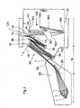
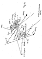
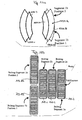
- FIG. 1 is a principle view of a projection exposure system for the production of, for example, microelectronic components, in which the invention can be used, shown.
- the projection exposure apparatus comprises a light source or an intermediate image of a light source 1.
- the light emitted by the light source 1 is collected by a collector 3 comprising a plurality of mirror shells.
- a further optical element which in the present case is designed as a plane mirror 300, follows the collector.
- the rays impinging on the plane mirror from the collector are deflected, in particular in order to provide installation space for the mechanical and optical components in an object plane 114 in which the wafer layer is arranged.
- the object plane 114 is also referred to as field level.
- the plane mirror 300 can also be designed as a diffractive spectral filter element.
- a diffractive spectral filter element is, for example, a grating as in the US Pat US-2002-0186811 A1 disclosed.
- a grating element is, for example, a grating as in the US Pat US-2002-0186811 A1 disclosed.
- unwanted radiation with, for example, wavelengths substantially greater than the desired wavelength from entering the part of the behind the aperture 302 illumination system.
- radiation with wavelengths not equal to the useful wavelength of, for example, 13.5 in EUV microlithography projection exposure systems can be prevented from entering the optical system behind the diaphragm 302.
- the aperture 302 can also serve to separate the space 304 comprising the light source and the collector 3 and the grid mirror 300 designed as a grid from the subsequent illumination system by introducing a valve near the intermediate focus Z, so that a 306 is also to be spatially separated. Both spaces are possible by pressure separation. By a spatial or a pressure separation can prevent dirt that originate from the light source 1, get into the behind the panel 302 lighting system.
- the light collected by the collector 3 and deflected via the plane mirror 300 is directed to a mirror 102 having a multiplicity of first raster elements, so-called field facets or field raster elements.
- the first raster elements are flat.
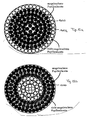
- the illumination in the plane 103 is arranged in or near the faceted mirror 102 can, as in the prior art according to FIG. 2 shown, be substantially circular, wherein each mirror shell of the collector depending an annular region is illuminated, which connects in the plane 103 substantially directly adjacent to annular regions.
- Such illumination for a collector according to the prior art as in US 2003-0043455A1 described is in FIG. 2 shown.
- a collector may be provided which has non-rotationally symmetrical, for example deformed mirror shells, so that a non-rotationally symmetrical, for example, a substantially rectangular illumination in the plane in which the first optical element 102 is arranged with field grid elements, is achieved.
- a collector with deformed mirror shells shows z. B. FIG. 4b ,
- a collector with rotationally symmetrical mirror shells can be provided to produce the substantially rectangular illumination, with an optical element, such as the optical element 300, which is arranged downstream of the collector in the light path, shaping the illumination in the FIGS. 6 and 7 described, takes over.
- the mirror 300 is formed aspherical, as in FIG. 6 shown.
- the lighting system is a double-faceted lighting system, such as in the US 6,198,793 B1 discloses and includes a first optical element 102 with field raster elements and a second optical element 104 with pupil raster elements.
- the second optical element 104 with pupil raster elements (not shown) is arranged in or near another plane, which is also referred to as the pupil plane 105.
- the light incident from the light source is decomposed by the faceted optical element 102 with field raster elements into a plurality of light bundles, wherein each field raster element is assigned exactly one pupil raster element of the second optical element.
- This assignment determines how in the US 2002-0136351 A1 shown, the illumination in the exit pupil of the illumination system.
- the exit pupil of the illumination system is usually given by the intersection of the main beam (CR) to the central field point in the field to be illuminated in the object plane 114 with the optical axis HA of the projection objective. This exit pupil is identified by the reference numeral 140 in the present exemplary embodiment.
- the optical elements 106, 108, 110 essentially serve to shape the field in the object plane 114.
- the field in the object plane 114 is usually a circular arc segment.
- an unrepresented reticle is arranged, which is illuminated with the aid of the illumination device 306 and imaged with the aid of the projection objective 128 into an image plane 124.
- the reticle arranged in the object plane 114 can be moved in direction 116.
- the exit pupil of the illumination system coincides with the entrance pupil of the projection objective 128.
- the field raster elements or field facets may have the shape of the field to be illuminated in the object plane and thus determine the shape of the field in the object plane.
- a lighting system is for example from the US 6,195,201 known. If the shape of the field in the object plane is, for example, circular-arc-shaped, the facets are likewise curved.
- the microlithography projection exposure systems are designed to be completely reflective with a useful wavelength of, for example, 13.5 nm for use in the field of EUV lithography, ie the field raster elements are designed as field facet mirrors and the pupil raster elements as pupil facet mirrors.
- the light source images are not object-true but are imaged in a pupil plane, for example the exit pupil.
- This can be compensated by aspherical field raster elements (not shown).
- Different field raster elements of the first optical element then preferably have different asphericities; depending on which asphericity is needed to compensate for the distortion caused by the illumination in the image of the light source image.
- the projection objective 128 in the illustrated embodiment has six mirrors 128.1, 128.2, 128.3, 128.4, 128.5 and 128.6 and is for example as in the US patent US 6,600,552 B2 educated.
- the projection objective 128 images the reticle (not shown) in the object plane 114 into the image plane 124.
- the illumination distribution in the plane 103 of the first optical element 102 is off FIG. 1 shown.
- the overall area A1 illuminated by the collector is defined by a boundary 400.1 originating from the outermost mirror shell and an inner boundary 400.2 originating from the innermost aperture element.
- the illumination in the plane 103 in FIG. 1 is circular.
- the field facets 402 of the first facetted optical element 102 in FIG. 1 are mirror elements which are arranged on a carrier.
- the field facets 402 have a substantially rectangular shape in the illustrated embodiment. In principle, field facets are also possible with a different shape, for example an arcuate shape, as described above.
- the geometric light loss of the illuminated area is approximately 40% compared to the area in which the field facets are arranged.
- Such optimized illumination in the field plane 103 according to FIG. 1 is in FIG. 3 shown.
- the substantially rectangular illumination A2 in the plane 103 in FIG. 1 again has an outer boundary 500.1 and an inner boundary 500.2.
- the field facets in FIG. 3 are designated by the reference numeral 502.
- the geometric light loss ie, the proportion of light that is not absorbed by the field facets, reduced to less than 10%, if the field facets are rectangular as shown.
- a substantially rectangular illumination in the plane 103 can be achieved in many different ways.
- the collector 3 according to FIG. 1 closed mirror surfaces which are arranged one inside the other about an axis of rotation.
- the deformation of the individual collector shells 602.1, 602.2, 602.3, 602.4, 602.5 directed inwards, ie towards the optical axis HA, is designated 605 and the outward directed deformation, ie directed away from the optical axis HA, is 607.
- the arrows 605 and 607 are perpendicular to the deformed collector surface. This is explained below.
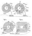
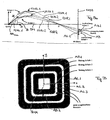
- Figure 4c is for a collector with a variety of undeformed to one common rotational axis HA rotationally symmetrical mirror shells 600.1, 600.2, 600.3, 600.4, 600.5, the illumination in the plane 103 shown.
- the common axis of rotation is also symmetry axis.
- illustrated illumination in the plane 103 in FIG. 1 is characterized by a center obscuration 700 and illuminations A3.1, A3.2, A3.3, A3.4, A3.5, which correspond to the respective mirror shells 600.1, 600.2, 600.3, 600.4 and 600.5 of the in FIG. 4a illustrated collector are associated with substantially rotationally symmetrical around the axis HA mirror shells, from.
- the illuminations A3.1, A3.2, A3.3, A3.4, A3.5 are in turn circular and essentially directly adjoin one another with a small gap.
- FIG. 4d is substantially rectangular in shape and has a central obturation 702 as well as the respective deformed mirror shells according to FIG. 4b associated illuminations A4.1, A4.2, A4.3, A4.4 and A4.5.
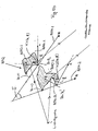
- a square illumination, as in FIG. 4d represented, due to the deformation of closed mirror surfaces can be achieved, for example, by the below-described design of a collector shell. Reference is made here FIG. 5a taken.
- the collector shell is composed of a base body, which is rotationally symmetrical about the optical axis HA, comprising a first hyperbolic mirror segment and an elliptical mirror segment adjoining the hyperbolic mirror segment.
- the hyperbolic first mirror segment 800 is obtained by rotation of a hyperboloid around the optical axis HA.
- the second rotationally symmetric elliptical mirror segment is in FIG. 5 shown in phantom and provided with reference numeral 802.
- the rotationally symmetric elliptical mirror segment is again obtained by rotation about the axis HA.
- the two components of the rotationally symmetrical basic body namely the first hyperbolic component 800 and the second elliptical component 802, are described by the following function.
- z H k ⁇ z 0 ⁇ h 2 1 + 1 - 1 + k ⁇ h ⁇ 2 + z 0 .
- k is the conic constant
- ⁇ is the curvature at the vertex.
- Table 1 Data for a rotationally symmetric mirror shell k ⁇ [mm -1 ] z 0 [mm] z 1 [mm] z 2 [mm] hyperboloid -1.26602359 0.04479337 -10,505 78374 159801 ellipsoid -0.96875135 0.03730042 -202361 159801 275000
- the collector shell shown in Table 1 above produces an annular illumination in the far field as in FIG Figure 4c shown.
- a targeted deviation of the elliptical component leads to rotational symmetry, which can be described by a correction in the normal direction of the basic body.
- the normal direction describes the direction that is perpendicular to the mirror shell at location z.
- Such a normal vector n is for different positions z in FIG. 5a shown.
- FIG. 5a Shown is the xyz coordinate system and the cylindrical coordinate system r, ⁇ in which the deviation from the rotational symmetry with which the substantially rectangular illumination in the plane 103 can be achieved, is described.
- the normal vector n is shown at each point of the rotationally symmetrical basic body.
- FIG. 4d shows the illumination in the plane 103 in FIG. 1 schematically.
- non-rotationally symmetric portion may be added or subtracted to the first hyperbolic mirror segment 800 (not shown) or to both mirror segments.
- a mirror may be formed in several pieces, wherein the mirror has sections of rotationally symmetric segments and sections not rotationally symmetric segments as described above.
- the segments can connect steadily or discontinuously to each other.
- a one-piece mirror is formed and in the second case a multi-piece mirror.
- a collector 852 as in FIG. 5b shown having at least one deformed mirror surface for generating any illumination including two surfaces 850.1, 850.2 as described below.
- Each of the two surfaces 850.1, 850.2 of the collector is defined by an axis 854.1, 854.2 and a surface function with respect to the respective axis.
- a z-axis 854.1, 854.2 is considered here for each surface.
- Perpendicular to each z-axis 854.1, 854.2 is an xy, plane 856.1, 856.2 for each Area that can be defined in polar coordinates by a radius r and an azimuth angle ⁇ .
- the area function K1, K2 of each area 850.1, 850.2 is a function of their respective z-coordinate and their respective azimuth angle ⁇ , wherein the azimuth angle may vary between 0 and 2 ⁇ .
- the azimuth angle ⁇ assumes values from 0 to 2 ⁇ . If only one mirror segment and no closed mirror surface are described, as shown here, the azimuth angle ⁇ assumes values between 0 and 2 ⁇ , for example from ⁇ / 2 to ⁇ .
- a surface in its most general form can be described by a curvature K (z, ⁇ ) dependent on z and the azimuth angle ⁇ .
- a surface function K1 (z, ⁇ ) results for the first surface 850.1 and K2 (z, ⁇ ) for the second surface 850.2.
- collectors are also conceivable which comprise more than two surfaces, for example three or four surfaces.
- the collector may also include the one-piece surface 850.2. Same reference numerals as in FIG. 5b will also be in FIG. 5c related.
- Each of the at least two adjacent surfaces is assigned in each case a local z-axis in the exemplary embodiment shown.
- a first z-axis 860.1 is associated with the first surface and a second z-axis 860.2 is associated with the second surface.
- the first and the second z-axis 860.1, 860.2 enclose an angle ⁇ with one another.
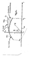
- an aspherical mirror 1105 may be arranged in the light path from the light source 1000 to the plane 1103 near the faceted optical element.
- the aspherical mirror 1300 transforms a substantially annular illumination 1007 generated by the collector 1003 with a plurality of mirror shells into a plane 1005 into a substantially rectangular illumination 1009 that is present in the plane 1103.
- FIG. 7 an alternative embodiment of the invention is shown in which a substantially annular illumination 1007 in a plane 1005 immediately adjacent to the collector 1003 by means of a grating 1302 with optical effect in a substantially rectangular, preferably square illumination 1011 in a plane 1103, in the the first optical element comes to rest with field raster elements, is transformed.
- the grating element 1302 diffracts the light into the first diffraction order.
- the light of the zeroth diffraction order which also contains wavelength components; which do not correspond to the wavelength of use can be prevented by an aperture from entering the lighting system.
- the useful wavelength is the wavelength used to image an object into an object plane into an image in an image plane in a microlithography projection exposure apparatus.
- a useful wavelength in EUV lithography would be a wavelength of 13.5 nm.
- FIG. 7 are the same components as in FIG. 6 with the same reference numerals. To the in FIG. 7 can be achieved in an illumination system according to FIG. 1 be provided to interpret the mirror 300 as a grating with optical effect.
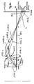
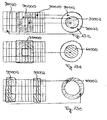
- FIG. 8a such a collector as in the US 2003-0043455A1 described in section through the xz plane.
- the source is designated by the reference numeral 1100, the first shell with reference numeral 1112.1 and the second shell with reference numeral 1112.2.
- the marginal rays 1114.1, 1114.2, 1116.1, 1116.2 of the first beam bundle 1118.1, which is received by the first collector shell 1112.1, and the second beam bundle 1118.2, which is received by the second collector shell 1112.2 are drawn.
- the marginal ray 1116 is drawn.
- the minimal collection NA Min determined by the in FIG. 8a shown collector of the light source 1100 can still be recorded.
- a diaphragm B is disposed in the interior of the second mirror shell 1112.2, which is closest to the axis of symmetry.
- the two beam tufts 1118.1, 1118.2 are reflected on the shells 1112.1, 1112.2 and shine in the plane 1103, which essentially corresponds to that in FIG FIG. 1 represented level 103, the areas A5.1 and A5.2 off.
- the two illuminations in plane 1103 are substantially directly adjacent to each other.
- the small gap existing between the illuminations which is smaller than 1 mm, is caused solely by the finite thickness of the individual reflector shells, ie the distance of the first and second illumination in the plane 1103 is less than 1 mm.
- the illumination in the plane 1103 in the xy direction for a system according to FIG. 8a is in FIG. 8b shown.
- FIG. 8b Clearly visible in FIG. 8b the individual ring segments A5.1, A5.2, A5.3, A5.4, A5.5. These individual ring segments are substantially directly adjacent to each other in the plane 1103. In FIG. 8b the symmetry axis of the illumination SMA is also shown.
- FIG. 8a only the first and second mirror shell is shown, whereas FIG. 8b also the illumination of the other mirror shells, namely the 3rd, 4th and 5th shell represents.
- the energy SE (x) integrated into the y-direction is SE (x) for the first shell with the illumination A5.1, for the second shell with the illumination A5. 2 and for the third shell with the illumination A5.3 shown.
- the scan-integrated energy for the first shell is designated by the reference numeral SE1, that for the second shell by the reference numeral SE2, and that for the third shell by the reference numeral SE3.
- the scan-integrated energy results from the integration of the contributions of the individual mirror shells along the y-axis of the ring field of the field plane 114 to be illuminated FIG. 1 the local coordinate system is specified at the field level. How out FIG. 1 it can be seen, the y-direction; which is also the direction of integration, the scan direction for the in FIG. 1 shown ring field projection exposure apparatus, which is operated in the scanning mode.
- the invention proposes that between the area illuminated by the first shell and the area illuminated by the second shell an unexposed area is provided, ie the first illumination is spaced from the second illumination, so that even with thermal deformation of the respective mirror shells the illuminations do not overlap. In this way, a largely homogeneous scan-integrated uniformity can be ensured.
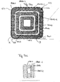
- FIG. 9a a system is shown in the xz-section, in which there is a distance AB between the illuminated area A6.1 and the illuminated area A6.2 of the first mirror shell 1212.1 and the second mirror shell 1212.2, respectively.
- the shells 1212.1, 1212.2 are preferably deformed collector shells, which in the plane 1102 not only lead to a distance between the illuminated areas, but also to a substantially rectangular shape of the illumination, as in FIG. 9b shown.
- NA Min the minimum collection aperture
- the diaphragm B is shown, which prevents the passage of stray light.
- the z-axis is shown, which at the same time in the present exemplary embodiment is also a common axis of symmetry for the closed, non-rotationally symmetrical mirror shells.
- FIG. 9b the illumination is shown for a total of 3 mirror shells, namely a first shell, a second shell and a third shell.
- the illuminated area of the first shell is denoted by A6.1
- the illuminated area of the second shell by A6.2
- the illuminated area of the third mirror shell by A6.3.
- the distances AB1 and AB2 are dimensioned such that upon deformation of the mirror shells, for example due to thermal deformation, the illuminated areas of the plane 1103 in which the first facetted optical element with field facets is arranged do not overlap.
- the illumination has an axis of symmetry SMA.
- the axis of symmetry SMA of the illumination is a fourfold symmetry axis.
- FIG. 9c the arrangement of the field facets in the illumination A6.1 of the first mirror shell in the plane 1103 is shown.
- the individual field facets are designated by reference numbers 1300.
- All field honeycombs 1300 lie within the illumination A6.1, which is enclosed by the solid lines 1320.1, 1320.2.
- the field honeycombs or field facets 1300 lying in the illumination A6.1 are completely illuminated.
- the illumination is largely rectangular and the shape of the field facets rectangular.
- the field facets lie in a region 1310 which is enclosed by the dot-dash lines 1310.1, 1310.2. This area encloses a surface B.
- the illumination ie the area A6.1 illuminated by the first mirror shell, has an area A.
- the geometric loss of light is minimized if the area 1310 in which the field facets come to rest is largely covered by the area A6.1, which is illuminated, for example, by the first collector shell. How out FIG. 9c It can be seen that only the corner regions E1, E2, E3, E4, E5, E6, E7, E8 of the illumination A6.1 are areas in which no grid elements are arranged. It is preferred if the area 1310 is completely illuminated, but the illumination is not more than 1.2 times the area B of the area 1310, ie for the area B of the area 1310 and the area A of the illumination A6.1, for example by the first mirror shell applies: A ⁇ B ⁇ 1 . 2 • A . prefers 1 . 05 • A ⁇ B ⁇ 1 . 1
- FIG. 9d is a first optical element with field raster elements which are adapted in shape to the illuminated field and the illumination of such a field raster element.
- field raster elements or field facets which have the shape of the field to be illuminated in the object plane, for example from US Pat US 6,195,201 known.
- US 6,195,201 is the shape of the field in the object plane circular arc, so that the individual field facets are also formed arcuate.
- the individual arcuate field facets are identified by the reference numeral 1350.
- the arcuate field facets are arranged in a region 1360 which is enclosed by the dot-dash lines 1360.1, 1360.2. Because the arcuate field facets.
- FIG. 1350 are arranged in this embodiment in a substantially rectangular area, the illumination caused by the collector A6a.1 in the plane in which the field facet elements are arranged, also largely rectangular.
- illumination is shown by a closed-face collector that includes but is not limited to a single mirror shell.
- multi-shell collectors can be used, as has been described in the case of rectangular field facets previously.
- other arrangements of the arcuate elements for example in blocks as for rectangular field honeycomb or field facets in FIG. 10b2 shown, possible.
- the field facets are for lighting systems or projection exposure systems, as in FIG. 1 shown reflectively for microlithography with wavelengths ⁇ 193 nm, in particular ⁇ 100 nm, in particular in the EUV wavelength range of ⁇ 15 nm are executed, also reflective, for example, designed as a single facet mirror.
- projection exposure equipment for lithography in the EUV wavelength range is only exemplary and by no means limiting for the invention.
- FIG. 10a the illumination achieved in the plane by means of the shell segments, in which the first facetted optical element with field facets or field raster elements is arranged, is in FIG. 10b shown.
- the first shell or mirror segment is designated by the reference numerals 1400.1, 1400.2, the second shell or mirror segment by the reference numerals 1400.3 and 1400.4.
- Figure 10b1-10b2 For example, the four illuminated areas are shown in the plane in which the first faceted element with field raster elements is arranged.
- FIG. 10b1 shows an embodiment with rectangular field facets.
- A7.1a and A7.2a denote the illumination in the plane 103 resulting from the mirror segment 1400.1 and 1400.2.
- the illuminations A8.1a and A8.2a denote the illuminations made by means of the mirror segments 1400.3 and 1400.4.
- the four areas A7.1a, A7.2a, A8.1a, A8.2a to be illuminated have a distance AB relative to each other.
- FIG. 10b.1 the rectangular field facets 1402.1 are all arranged within the illuminated regions A7.1a, A7.2a, A8.1a, A8.2a.
- FIG. 10b.2 an embodiment of the invention is shown in which the field facets 1402.2 is arcuate.
- the areas illuminated by the mirror segments 1400.1 and 1400.2 are denoted by A7.1b, A 7.2b, A8.1b and A8.2b.
- the distances between the illuminations are again indicated by AB.
- FIG. 11a is a further developed, in Figure 11a and Figure 11b
- the collector can be operated in two states, namely in a first and in a second position.
- the collector is then in the plane 103 in FIG. 1 in which the first faceted optical element with field facets is arranged, in each case a different area of field facets is illuminated.
- a collector is composed of two shell segments 1500.1, 1500.2, 1500.3 and 1500.4. Segment 1500.2 can be moved to two positions 1500.2A and 1500.2B.
- FIG. 11b is the associated illumination in the plane 103 according to FIG.
- the rotatable segment 1500.2 has the illumination A9.1A in position 1500.2A and the illumination A9.1B in position 1500.2B. How to clear FIG. 11b detects can be set by turning the segment 1500.2 in the two specified positions a different illumination.
- FIGS. 12a and 12b the illumination is shown on the second faceted optical element 104 with pupil facets.
- the illumination according to FIG. 12a that is, the outermost pupil facets 1600 are not illuminated, the inner pupil facets 1602 are illuminated, resulting in a conventional circular setting in the exit pupil.
- the segment 1502 is moved to the second position 1502B, the illumination according to FIG. 12b , The illuminated pupil facets 1600 are located in the outer area, the unilluminated pupil facets in the inner area. It then results in the exit pupil an annular setting.
- a so-called roof edge mirror 10000 is shown, which is rotatable about an axis A and can be moved to two different positions.
- the roof edge mirror acts as a first mirror 8000 in the light path like a plane mirror, such as the in FIG. 1 plane mirror 300 shown.
- the illumination on the optical element, which in FIG. 1 102, and thus the first raster elements, is determined, for example, by the shape of the mirror shells of the collector 3.
- the light beam, which impinges on the planar part 10002 of the roof edge mirror from a light source, not shown, is reflected without division onto the optical element with first raster elements.
- the roof edge mirror 10000 about the optical axis A in the in FIG. 13b rotated position shown so is a light beam 10004, that of a Light source, not shown, impinges on the roof edge mirror, divided into two light bundles 10004.1 and 10004.2, and illuminates two areas 9002.1, 9002.2 of the field facet mirror.
- other first raster elements ie field raster elements like in FIG. 13a can be illuminated, by assigning field facets to pupil facets, as in the FIGS. 13b to 13c shown, each set a different setting in the exit pupil.
- the roof edge mirror provides a second and third reflective surface in the form of a second mirror 8002 having two reflective surfaces 8004.1, 8004.2.
- the field raster elements in the region 30000 are assigned to the pupil raster elements in the region 30002, the field raster elements in the region 30010 to the pupil raster elements in the region 30012 and the field raster elements 30020 to the pupil raster elements 30022.
- FIG. 13d shown an area 35000 as in FIG. 13a Illuminated shown on the optical element with field raster elements, so a conventional filled pupil 40000 is substantially illuminated.
- an illumination 35002 according to FIG. 13e set on the optical element with field raster elements In the pupil, a circular illumination 40002 is realized because by the illumination of other field raster elements than in FIG. 13c other pupil grid elements are illuminated, which in turn lead to a different illumination in the exit pupil of the illumination system.
- a rotatable roof edge mirror instead of changing the illumination of the first optical element with field raster elements via a rotatable roof edge mirror, it is also possible to change the mirror element and thus achieve different illumination on the first raster element, for example with the aid of a mirror changer, for example one Mirror wheel are arranged on the different mirrors. For example, a plane mirror or even tilted mirrors with two mirror surfaces or with aspherical surfaces can be arranged on the mirror wheel.
- a collector for an EUV projection lens is given, compared to those from the US 2003-0043455A1 known collectors having an illumination with a lower geometric light loss.
- fluctuations in the scan-integrated energy in the field plane for example due to deformations of the individual mirror shells, are reduced.
- the present invention includes the aspects set forth in the following sentences, which form a part of the specification, but are not claims in accordance with the Board of Appeal's decision J15 / 88:
Landscapes
- Physics & Mathematics (AREA)
- General Physics & Mathematics (AREA)
- Engineering & Computer Science (AREA)
- Chemical & Material Sciences (AREA)
- Nanotechnology (AREA)
- Mathematical Physics (AREA)
- Theoretical Computer Science (AREA)
- Crystallography & Structural Chemistry (AREA)
- Lenses (AREA)
- Exposure Of Semiconductors, Excluding Electron Or Ion Beam Exposure (AREA)
- Optical Elements Other Than Lenses (AREA)
- Exposure And Positioning Against Photoresist Photosensitive Materials (AREA)
Applications Claiming Priority (2)
| Application Number | Priority Date | Filing Date | Title |
|---|---|---|---|
| US72789205P | 2005-10-18 | 2005-10-18 | |
| PCT/EP2006/010004 WO2007045434A2 (de) | 2005-10-18 | 2006-10-17 | Kollektor für beleuchtungssysteme mit einer wellenlänge ≤ 193 nm |
Publications (2)
| Publication Number | Publication Date |
|---|---|
| EP1938150A2 EP1938150A2 (de) | 2008-07-02 |
| EP1938150B1 true EP1938150B1 (de) | 2011-03-23 |
Family
ID=37698183
Family Applications (1)
| Application Number | Title | Priority Date | Filing Date |
|---|---|---|---|
| EP06806336A Not-in-force EP1938150B1 (de) | 2005-10-18 | 2006-10-17 | Kollektor für beleuchtungssysteme mit einer wellenlänge </= 193 nm |
Country Status (5)
| Country | Link |
|---|---|
| US (1) | US20080225387A1 (enExample) |
| EP (1) | EP1938150B1 (enExample) |
| JP (1) | JP4990287B2 (enExample) |
| DE (1) | DE502006009171D1 (enExample) |
| WO (1) | WO2007045434A2 (enExample) |
Families Citing this family (18)
| Publication number | Priority date | Publication date | Assignee | Title |
|---|---|---|---|---|
| DE102007045396A1 (de) | 2007-09-21 | 2009-04-23 | Carl Zeiss Smt Ag | Bündelführender optischer Kollektor zur Erfassung der Emission einer Strahlungsquelle |
| EP2083327B1 (en) * | 2008-01-28 | 2017-11-29 | Media Lario s.r.l. | Improved grazing incidence collector optical systems for EUV and X-ray applications |
| DE102008000967B4 (de) * | 2008-04-03 | 2015-04-09 | Carl Zeiss Smt Gmbh | Projektionsbelichtungsanlage für die EUV-Mikrolithographie |
| DE102009030501A1 (de) * | 2009-06-24 | 2011-01-05 | Carl Zeiss Smt Ag | Abbildende Optik zur Abbildung eines Objektfeldes in ein Bildfeld sowie Beleuchtungsoptik zur Ausleuchtung eines Objektfeldes |
| DE102009054540B4 (de) * | 2009-12-11 | 2011-11-10 | Carl Zeiss Smt Gmbh | Beleuchtungsoptik für die EUV-Mikrolithographie |
| EP2517066B1 (en) * | 2009-12-21 | 2022-02-23 | Harman Professional Denmark ApS | Projecting illumination device with multiple light sources |
| KR102160046B1 (ko) | 2010-04-02 | 2020-09-28 | 가부시키가이샤 니콘 | 조명 광학계, 노광 방법 및 디바이스 제조 방법 |
| DE102010029049B4 (de) * | 2010-05-18 | 2014-03-13 | Carl Zeiss Smt Gmbh | Beleuchtungsoptik für ein Metrologiesystem für die Untersuchung eines Objekts mit EUV-Beleuchtungslicht sowie Metrologiesystem mit einer derartigen Beleuchtungsoptik |
| DE102011016058B4 (de) * | 2011-04-01 | 2012-11-29 | Xtreme Technologies Gmbh | Verfahren und Vorrichtung zur Einstellung von Eigenschaften eines Strahlenbündels aus einem Plasma emittierter hochenergetischer Strahlung |
| DE102011076297A1 (de) * | 2011-05-23 | 2012-11-29 | Carl Zeiss Smt Gmbh | Blende |
| DE102011076460A1 (de) * | 2011-05-25 | 2012-11-29 | Carl Zeiss Smt Gmbh | Beleuchtungsoptik |
| DE102013204441A1 (de) | 2013-03-14 | 2014-04-03 | Carl Zeiss Smt Gmbh | Kollektor |
| DE102013218132A1 (de) | 2013-09-11 | 2015-03-12 | Carl Zeiss Smt Gmbh | Kollektor |
| DE102013218128A1 (de) | 2013-09-11 | 2015-03-12 | Carl Zeiss Smt Gmbh | Beleuchtungssystem |
| DE102015201138A1 (de) * | 2015-01-23 | 2016-01-28 | Carl Zeiss Smt Gmbh | Beleuchtungsoptik für die EUV-Projektionslithografie |
| DE102018207103A1 (de) | 2018-05-08 | 2019-03-21 | Carl Zeiss Smt Gmbh | Feldfacettenspiegel |
| DE102018214559A1 (de) | 2018-08-28 | 2019-09-12 | Carl Zeiss Smt Gmbh | Optische Anordnung und EUV-Lithographievorrichtung damit |
| US11543753B2 (en) | 2019-10-30 | 2023-01-03 | Taiwan Semiconductor Manufacturing Co., Ltd. | Tunable illuminator for lithography systems |
Family Cites Families (18)
| Publication number | Priority date | Publication date | Assignee | Title |
|---|---|---|---|---|
| US2077740A (en) * | 1934-03-30 | 1937-04-20 | Martha W Caughlan | Reflecting surface |
| DE3340462C1 (de) * | 1983-11-09 | 1985-04-18 | Westfälische Metall Industrie KG Hueck & Co, 4780 Lippstadt | Abgeblendeter Fahrzeugscheinwerfer |
| DE10138313A1 (de) | 2001-01-23 | 2002-07-25 | Zeiss Carl | Kollektor für Beleuchtugnssysteme mit einer Wellenlänge < 193 nm |
| DE10053587A1 (de) * | 2000-10-27 | 2002-05-02 | Zeiss Carl | Beleuchtungssystem mit variabler Einstellung der Ausleuchtung |
| EP0955641B1 (de) | 1998-05-05 | 2004-04-28 | Carl Zeiss | Beleuchtungssystem insbesondere für die EUV-Lithographie |
| US6195201B1 (en) * | 1999-01-27 | 2001-02-27 | Svg Lithography Systems, Inc. | Reflective fly's eye condenser for EUV lithography |
| US6600552B2 (en) * | 1999-02-15 | 2003-07-29 | Carl-Zeiss Smt Ag | Microlithography reduction objective and projection exposure apparatus |
| US7248667B2 (en) * | 1999-05-04 | 2007-07-24 | Carl Zeiss Smt Ag | Illumination system with a grating element |
| DE19935568A1 (de) * | 1999-07-30 | 2001-02-15 | Zeiss Carl Fa | Steuerung der Beleuchtungsverteilung in der Austrittspupille eines EUV-Beleuchtungssystems |
| DE10138284A1 (de) * | 2001-08-10 | 2003-02-27 | Zeiss Carl | Beleuchtungssystem mit genesteten Kollektoren |
| WO2003014833A2 (de) * | 2001-08-10 | 2003-02-20 | Carl Zeiss Smt Ag | Kollektor mit befestigungseinrichtungen zum befestigen von spiegelschalen |
| DE10208854A1 (de) * | 2002-03-01 | 2003-09-04 | Zeiss Carl Semiconductor Mfg | Beleuchtungssystem mit genestetem Kollektor zur annularen Ausleuchtung einer Austrittspupille |
| US7084412B2 (en) * | 2002-03-28 | 2006-08-01 | Carl Zeiss Smt Ag | Collector unit with a reflective element for illumination systems with a wavelength of smaller than 193 nm |
| DE10214259A1 (de) | 2002-03-28 | 2003-10-23 | Zeiss Carl Semiconductor Mfg | Kollektoreinheit für Beleuchtungssysteme mit einer Wellenlänge <193 nm |
| DE10219514A1 (de) * | 2002-04-30 | 2003-11-13 | Zeiss Carl Smt Ag | Beleuchtungssystem, insbesondere für die EUV-Lithographie |
| EP1573402B1 (en) * | 2002-12-19 | 2008-03-12 | Carl Zeiss SMT AG | Illumination system having a more efficient collector optic |
| US7481544B2 (en) * | 2004-03-05 | 2009-01-27 | Optical Research Associates | Grazing incidence relays |
| JP2006245147A (ja) * | 2005-03-01 | 2006-09-14 | Canon Inc | 投影光学系、露光装置及びデバイスの製造方法 |
-
2006
- 2006-10-17 WO PCT/EP2006/010004 patent/WO2007045434A2/de not_active Ceased
- 2006-10-17 EP EP06806336A patent/EP1938150B1/de not_active Not-in-force
- 2006-10-17 JP JP2008535955A patent/JP4990287B2/ja not_active Expired - Fee Related
- 2006-10-17 DE DE502006009171T patent/DE502006009171D1/de active Active
-
2008
- 2008-03-21 US US12/053,305 patent/US20080225387A1/en not_active Abandoned
Also Published As
| Publication number | Publication date |
|---|---|
| DE502006009171D1 (de) | 2011-05-05 |
| WO2007045434A2 (de) | 2007-04-26 |
| JP4990287B2 (ja) | 2012-08-01 |
| EP1938150A2 (de) | 2008-07-02 |
| US20080225387A1 (en) | 2008-09-18 |
| WO2007045434A3 (de) | 2007-07-19 |
| JP2009512223A (ja) | 2009-03-19 |
Similar Documents
| Publication | Publication Date | Title |
|---|---|---|
| EP1938150B1 (de) | Kollektor für beleuchtungssysteme mit einer wellenlänge </= 193 nm | |
| EP1076906B1 (de) | Beleuchtungssystem insbesondere für die euv-lithographie | |
| DE102012202057B4 (de) | Projektionsobjektiv für EUV-Mikrolithographie, Folienelement und Verfahren zur Herstellung eines Projektionsobjektivs mit Folienelement | |
| DE102011003928B4 (de) | Beleuchtungsoptik für die Projektionslithographie | |
| EP1884831A2 (de) | Beleuchtungssystem für eine Projektionsbelichtungsanlage mit Wellenlängen < 193 nm | |
| DE19903807A1 (de) | Beleuchtungssystem insbesondere für die EUV-Lithographie | |
| DE10138284A1 (de) | Beleuchtungssystem mit genesteten Kollektoren | |
| DE10317667A1 (de) | Optisches Element für ein Beleuchtungssystem | |
| DE102014203187A1 (de) | Beleuchtungsoptik für die Projektionslithografie | |
| DE102006014380A1 (de) | Projektionsobjektiv und Projektionsbelichtungsanlage mit negativer Schnittweite der Eintrittspupille | |
| DE102008049586A1 (de) | Feldfacettenspiegel zum Einsatz in einer Beleuchtungsoptik einer Projektionsbelichtungsanlage für die EUV-Mikrolithographie | |
| EP1845417B1 (de) | Beleuchtungssystem mit Zoomobjetiv | |
| DE102009030501A1 (de) | Abbildende Optik zur Abbildung eines Objektfeldes in ein Bildfeld sowie Beleuchtungsoptik zur Ausleuchtung eines Objektfeldes | |
| DE102010040108A1 (de) | Obskurationsblende | |
| DE102012207377A1 (de) | Beleuchtungsoptik sowie optisches System für die EUV-Projektionslithographie | |
| DE102022200372A1 (de) | Verfahren zum Nachbilden von Beleuchtungs- und Abbildungseigenschaften eines optischen Produktionssystems bei der Beleuchtung und Abbildung eines Objekts mittels eines optischen Messsystems | |
| DE102009006685A1 (de) | Beleuchtungssystem für die Mikro-Lithographie | |
| DE102006059024A1 (de) | Projektionsbelichtungsanlage für die Mikrolithographie, Beleuchtungsoptik für eine derartige Projektionsbelichtungsanlage, Verfahren zum Betrieb einer derartigen Projektionsbelichtungsanlage, Verfahren zur Herstellung eines mikrostrukturierten Bauteils sowie durch das Verfahren hergestelltes mikrostrukturiertes Bauteil | |
| EP1481276A1 (de) | Beleuchtungssystem mit genestetem kollektor zur annularen ausleuchtung einer austrittspupille | |
| DE102012207866A1 (de) | Baugruppe für eine Projektionsbelichtungsanlage für die EUV-Projektionslithografie | |
| DE10037870A1 (de) | 6-Spiegel-Mikrolithographie-Projektionsobjektiv | |
| DE102018201457A1 (de) | Beleuchtungsoptik für die Projektionslithographie | |
| DE60319735T2 (de) | Beleuchtungssytem mit einer effizienteren kollektoroptik | |
| DE102022206110A1 (de) | Abbildende EUV-Optik zur Abbildung eines Objektfeldes in ein Bildfeld | |
| WO2005036266A1 (de) | Masken, lithographievorrichtung und halbleiterbauelement |
Legal Events
| Date | Code | Title | Description |
|---|---|---|---|
| PUAI | Public reference made under article 153(3) epc to a published international application that has entered the european phase |
Free format text: ORIGINAL CODE: 0009012 |
|
| 17P | Request for examination filed |
Effective date: 20080213 |
|
| AK | Designated contracting states |
Kind code of ref document: A2 Designated state(s): DE FR IT NL |
|
| DAX | Request for extension of the european patent (deleted) | ||
| RBV | Designated contracting states (corrected) |
Designated state(s): DE FR IT NL |
|
| 17Q | First examination report despatched |
Effective date: 20100823 |
|
| GRAP | Despatch of communication of intention to grant a patent |
Free format text: ORIGINAL CODE: EPIDOSNIGR1 |
|
| RTI1 | Title (correction) |
Free format text: COLLECTOR FOR LIGHTING SYSTEMS WITH A WAVELENGTH SMALLER/EQUAL 193 NM |
|
| GRAS | Grant fee paid |
Free format text: ORIGINAL CODE: EPIDOSNIGR3 |
|
| GRAA | (expected) grant |
Free format text: ORIGINAL CODE: 0009210 |
|
| RAP1 | Party data changed (applicant data changed or rights of an application transferred) |
Owner name: CARL ZEISS SMT GMBH |
|
| AK | Designated contracting states |
Kind code of ref document: B1 Designated state(s): DE FR IT NL |
|
| REF | Corresponds to: |
Ref document number: 502006009171 Country of ref document: DE Date of ref document: 20110505 Kind code of ref document: P |
|
| REG | Reference to a national code |
Ref country code: DE Ref legal event code: R096 Ref document number: 502006009171 Country of ref document: DE Effective date: 20110505 |
|
| REG | Reference to a national code |
Ref country code: NL Ref legal event code: T3 |
|
| PLBE | No opposition filed within time limit |
Free format text: ORIGINAL CODE: 0009261 |
|
| 26N | No opposition filed |
Effective date: 20111227 |
|
| REG | Reference to a national code |
Ref country code: DE Ref legal event code: R097 Ref document number: 502006009171 Country of ref document: DE Effective date: 20111227 |
|
| REG | Reference to a national code |
Ref country code: FR Ref legal event code: ST Effective date: 20120629 |
|
| PG25 | Lapsed in a contracting state [announced via postgrant information from national office to epo] |
Ref country code: FR Free format text: LAPSE BECAUSE OF NON-PAYMENT OF DUE FEES Effective date: 20111102 |
|
| PGFP | Annual fee paid to national office [announced via postgrant information from national office to epo] |
Ref country code: DE Payment date: 20171019 Year of fee payment: 12 |
|
| PGFP | Annual fee paid to national office [announced via postgrant information from national office to epo] |
Ref country code: IT Payment date: 20171023 Year of fee payment: 12 |
|
| PLAA | Information modified related to event that no opposition was filed |
Free format text: ORIGINAL CODE: 0009299DELT |
|
| STAA | Information on the status of an ep patent application or granted ep patent |
Free format text: STATUS: NO OPPOSITION FILED WITHIN TIME LIMIT |
|
| PLBE | No opposition filed within time limit |
Free format text: ORIGINAL CODE: 0009261 |
|
| PGFP | Annual fee paid to national office [announced via postgrant information from national office to epo] |
Ref country code: NL Payment date: 20181019 Year of fee payment: 13 |
|
| D26N | No opposition filed (deleted) | ||
| RIN2 | Information on inventor provided after grant (corrected) |
Inventor name: ENDRES, MARTIN Inventor name: BADER, DIETER Inventor name: HAINZ, JOACHIM Inventor name: SINGER, WOLFGANG Inventor name: KLEEMANN, BERND |
|
| 26N | No opposition filed |
Effective date: 20111227 |
|
| REG | Reference to a national code |
Ref country code: DE Ref legal event code: R119 Ref document number: 502006009171 Country of ref document: DE |
|
| PG25 | Lapsed in a contracting state [announced via postgrant information from national office to epo] |
Ref country code: DE Free format text: LAPSE BECAUSE OF NON-PAYMENT OF DUE FEES Effective date: 20190501 |
|
| PG25 | Lapsed in a contracting state [announced via postgrant information from national office to epo] |
Ref country code: IT Free format text: LAPSE BECAUSE OF NON-PAYMENT OF DUE FEES Effective date: 20181017 |
|
| REG | Reference to a national code |
Ref country code: NL Ref legal event code: MM Effective date: 20191101 |
|
| PG25 | Lapsed in a contracting state [announced via postgrant information from national office to epo] |
Ref country code: NL Free format text: LAPSE BECAUSE OF NON-PAYMENT OF DUE FEES Effective date: 20191101 |