EP1933382A2 - Phasenwechsel-RAM-Speichervorrichtung mit Transistor und Verfahren zur Herstellung einer Speichervorrichtung - Google Patents
Phasenwechsel-RAM-Speichervorrichtung mit Transistor und Verfahren zur Herstellung einer Speichervorrichtung Download PDFInfo
- Publication number
- EP1933382A2 EP1933382A2 EP07021307A EP07021307A EP1933382A2 EP 1933382 A2 EP1933382 A2 EP 1933382A2 EP 07021307 A EP07021307 A EP 07021307A EP 07021307 A EP07021307 A EP 07021307A EP 1933382 A2 EP1933382 A2 EP 1933382A2
- Authority
- EP
- European Patent Office
- Prior art keywords
- nanotube
- integrated circuit
- active material
- volume
- switching active
- Prior art date
- Legal status (The legal status is an assumption and is not a legal conclusion. Google has not performed a legal analysis and makes no representation as to the accuracy of the status listed.)
- Withdrawn
Links
- 238000000034 method Methods 0.000 title claims abstract description 26
- 230000008859 change Effects 0.000 title abstract description 8
- 239000002071 nanotube Substances 0.000 claims abstract description 67
- 239000011149 active material Substances 0.000 claims abstract description 61
- 239000002070 nanowire Substances 0.000 claims abstract description 45
- 239000004020 conductor Substances 0.000 claims abstract description 44
- XUIMIQQOPSSXEZ-UHFFFAOYSA-N Silicon Chemical compound [Si] XUIMIQQOPSSXEZ-UHFFFAOYSA-N 0.000 claims description 43
- 229910052710 silicon Inorganic materials 0.000 claims description 43
- 239000010703 silicon Substances 0.000 claims description 43
- 125000006850 spacer group Chemical group 0.000 claims description 28
- 238000000151 deposition Methods 0.000 claims description 27
- 239000000463 material Substances 0.000 claims description 26
- 239000003054 catalyst Substances 0.000 claims description 18
- VYPSYNLAJGMNEJ-UHFFFAOYSA-N Silicium dioxide Chemical compound O=[Si]=O VYPSYNLAJGMNEJ-UHFFFAOYSA-N 0.000 claims description 12
- NRTOMJZYCJJWKI-UHFFFAOYSA-N Titanium nitride Chemical group [Ti]#N NRTOMJZYCJJWKI-UHFFFAOYSA-N 0.000 claims description 9
- 230000008878 coupling Effects 0.000 claims description 5
- 238000010168 coupling process Methods 0.000 claims description 5
- 238000005859 coupling reaction Methods 0.000 claims description 5
- 229910052751 metal Inorganic materials 0.000 claims description 5
- 239000002184 metal Substances 0.000 claims description 5
- 239000012782 phase change material Substances 0.000 claims description 5
- 229910052814 silicon oxide Inorganic materials 0.000 claims description 4
- KRHYYFGTRYWZRS-UHFFFAOYSA-N Fluorane Chemical compound F KRHYYFGTRYWZRS-UHFFFAOYSA-N 0.000 claims description 3
- PXHVJJICTQNCMI-UHFFFAOYSA-N Nickel Chemical compound [Ni] PXHVJJICTQNCMI-UHFFFAOYSA-N 0.000 claims description 3
- 229910000040 hydrogen fluoride Inorganic materials 0.000 claims description 2
- 229910052759 nickel Inorganic materials 0.000 claims description 2
- 229910021332 silicide Inorganic materials 0.000 claims description 2
- FVBUAEGBCNSCDD-UHFFFAOYSA-N silicide(4-) Chemical compound [Si-4] FVBUAEGBCNSCDD-UHFFFAOYSA-N 0.000 claims description 2
- 229910017052 cobalt Inorganic materials 0.000 claims 1
- 239000010941 cobalt Substances 0.000 claims 1
- GUTLYIVDDKVIGB-UHFFFAOYSA-N cobalt atom Chemical compound [Co] GUTLYIVDDKVIGB-UHFFFAOYSA-N 0.000 claims 1
- 230000007423 decrease Effects 0.000 claims 1
- 239000010410 layer Substances 0.000 description 30
- 238000012545 processing Methods 0.000 description 18
- 238000005530 etching Methods 0.000 description 14
- 229920002120 photoresistant polymer Polymers 0.000 description 13
- 230000008569 process Effects 0.000 description 10
- 239000011810 insulating material Substances 0.000 description 9
- 230000015572 biosynthetic process Effects 0.000 description 7
- 239000011229 interlayer Substances 0.000 description 7
- 229910052721 tungsten Inorganic materials 0.000 description 7
- 238000011049 filling Methods 0.000 description 6
- 238000010438 heat treatment Methods 0.000 description 6
- WFKWXMTUELFFGS-UHFFFAOYSA-N tungsten Chemical compound [W] WFKWXMTUELFFGS-UHFFFAOYSA-N 0.000 description 6
- 239000010937 tungsten Substances 0.000 description 6
- 238000005229 chemical vapour deposition Methods 0.000 description 5
- 230000008021 deposition Effects 0.000 description 5
- HBMJWWWQQXIZIP-UHFFFAOYSA-N silicon carbide Chemical compound [Si+]#[C-] HBMJWWWQQXIZIP-UHFFFAOYSA-N 0.000 description 5
- 229910010271 silicon carbide Inorganic materials 0.000 description 5
- 229910052581 Si3N4 Inorganic materials 0.000 description 4
- 229910052681 coesite Inorganic materials 0.000 description 4
- 238000007796 conventional method Methods 0.000 description 4
- 229910052906 cristobalite Inorganic materials 0.000 description 4
- 239000000377 silicon dioxide Substances 0.000 description 4
- HQVNEWCFYHHQES-UHFFFAOYSA-N silicon nitride Chemical compound N12[Si]34N5[Si]62N3[Si]51N64 HQVNEWCFYHHQES-UHFFFAOYSA-N 0.000 description 4
- 229910052682 stishovite Inorganic materials 0.000 description 4
- 229910052905 tridymite Inorganic materials 0.000 description 4
- 235000012239 silicon dioxide Nutrition 0.000 description 3
- LIVNPJMFVYWSIS-UHFFFAOYSA-N silicon monoxide Chemical compound [Si-]#[O+] LIVNPJMFVYWSIS-UHFFFAOYSA-N 0.000 description 3
- 238000003786 synthesis reaction Methods 0.000 description 3
- OKTJSMMVPCPJKN-UHFFFAOYSA-N Carbon Chemical compound [C] OKTJSMMVPCPJKN-UHFFFAOYSA-N 0.000 description 2
- 238000000231 atomic layer deposition Methods 0.000 description 2
- 239000002041 carbon nanotube Substances 0.000 description 2
- 229910021393 carbon nanotube Inorganic materials 0.000 description 2
- -1 chalcogenide compound Chemical class 0.000 description 2
- 150000004770 chalcogenides Chemical class 0.000 description 2
- AIOWANYIHSOXQY-UHFFFAOYSA-N cobalt silicon Chemical compound [Si].[Co] AIOWANYIHSOXQY-UHFFFAOYSA-N 0.000 description 2
- 239000007943 implant Substances 0.000 description 2
- 238000005468 ion implantation Methods 0.000 description 2
- 150000002500 ions Chemical class 0.000 description 2
- 238000002955 isolation Methods 0.000 description 2
- 238000004519 manufacturing process Methods 0.000 description 2
- 229910021421 monocrystalline silicon Inorganic materials 0.000 description 2
- 239000002121 nanofiber Substances 0.000 description 2
- PEUPIGGLJVUNEU-UHFFFAOYSA-N nickel silicon Chemical compound [Si].[Ni] PEUPIGGLJVUNEU-UHFFFAOYSA-N 0.000 description 2
- 229910021420 polycrystalline silicon Inorganic materials 0.000 description 2
- 229920005591 polysilicon Polymers 0.000 description 2
- 238000007493 shaping process Methods 0.000 description 2
- 229910052580 B4C Inorganic materials 0.000 description 1
- PZNSFCLAULLKQX-UHFFFAOYSA-N Boron nitride Chemical compound N#B PZNSFCLAULLKQX-UHFFFAOYSA-N 0.000 description 1
- 101100126625 Caenorhabditis elegans itr-1 gene Proteins 0.000 description 1
- 229910007991 Si-N Inorganic materials 0.000 description 1
- 229910006294 Si—N Inorganic materials 0.000 description 1
- 230000006978 adaptation Effects 0.000 description 1
- 238000013459 approach Methods 0.000 description 1
- QVGXLLKOCUKJST-UHFFFAOYSA-N atomic oxygen Chemical compound [O] QVGXLLKOCUKJST-UHFFFAOYSA-N 0.000 description 1
- 230000006399 behavior Effects 0.000 description 1
- INAHAJYZKVIDIZ-UHFFFAOYSA-N boron carbide Chemical compound B12B3B4C32B41 INAHAJYZKVIDIZ-UHFFFAOYSA-N 0.000 description 1
- 238000012512 characterization method Methods 0.000 description 1
- 238000006243 chemical reaction Methods 0.000 description 1
- 229910052804 chromium Inorganic materials 0.000 description 1
- 230000015271 coagulation Effects 0.000 description 1
- 238000005345 coagulation Methods 0.000 description 1
- 150000001875 compounds Chemical class 0.000 description 1
- 239000012141 concentrate Substances 0.000 description 1
- 238000001816 cooling Methods 0.000 description 1
- 229910052802 copper Inorganic materials 0.000 description 1
- 238000002425 crystallisation Methods 0.000 description 1
- 230000008025 crystallization Effects 0.000 description 1
- 238000007323 disproportionation reaction Methods 0.000 description 1
- 230000000694 effects Effects 0.000 description 1
- 229910052737 gold Inorganic materials 0.000 description 1
- 229910052735 hafnium Inorganic materials 0.000 description 1
- 238000011835 investigation Methods 0.000 description 1
- 229910052741 iridium Inorganic materials 0.000 description 1
- 229910052748 manganese Inorganic materials 0.000 description 1
- 239000011859 microparticle Substances 0.000 description 1
- 229910052750 molybdenum Inorganic materials 0.000 description 1
- 239000005543 nano-size silicon particle Substances 0.000 description 1
- 230000003287 optical effect Effects 0.000 description 1
- 229910052760 oxygen Inorganic materials 0.000 description 1
- 239000001301 oxygen Substances 0.000 description 1
- 229910052763 palladium Inorganic materials 0.000 description 1
- 230000037361 pathway Effects 0.000 description 1
- 238000001020 plasma etching Methods 0.000 description 1
- 229910052697 platinum Inorganic materials 0.000 description 1
- 238000005498 polishing Methods 0.000 description 1
- 238000003672 processing method Methods 0.000 description 1
- 239000011253 protective coating Substances 0.000 description 1
- 238000010791 quenching Methods 0.000 description 1
- 238000011160 research Methods 0.000 description 1
- 229910052703 rhodium Inorganic materials 0.000 description 1
- 239000000126 substance Substances 0.000 description 1
- 238000006467 substitution reaction Methods 0.000 description 1
- 229910052715 tantalum Inorganic materials 0.000 description 1
- 239000010936 titanium Substances 0.000 description 1
- 229910052719 titanium Inorganic materials 0.000 description 1
- 229910052726 zirconium Inorganic materials 0.000 description 1
Images







Classifications
-
- G—PHYSICS
- G11—INFORMATION STORAGE
- G11C—STATIC STORES
- G11C11/00—Digital stores characterised by the use of particular electric or magnetic storage elements; Storage elements therefor
- G11C11/56—Digital stores characterised by the use of particular electric or magnetic storage elements; Storage elements therefor using storage elements with more than two stable states represented by steps, e.g. of voltage, current, phase, frequency
- G11C11/5678—Digital stores characterised by the use of particular electric or magnetic storage elements; Storage elements therefor using storage elements with more than two stable states represented by steps, e.g. of voltage, current, phase, frequency using amorphous/crystalline phase transition storage elements
-
- H—ELECTRICITY
- H10—SEMICONDUCTOR DEVICES; ELECTRIC SOLID-STATE DEVICES NOT OTHERWISE PROVIDED FOR
- H10B—ELECTRONIC MEMORY DEVICES
- H10B63/00—Resistance change memory devices, e.g. resistive RAM [ReRAM] devices
- H10B63/30—Resistance change memory devices, e.g. resistive RAM [ReRAM] devices comprising selection components having three or more electrodes, e.g. transistors
-
- H—ELECTRICITY
- H10—SEMICONDUCTOR DEVICES; ELECTRIC SOLID-STATE DEVICES NOT OTHERWISE PROVIDED FOR
- H10B—ELECTRONIC MEMORY DEVICES
- H10B63/00—Resistance change memory devices, e.g. resistive RAM [ReRAM] devices
- H10B63/80—Arrangements comprising multiple bistable or multi-stable switching components of the same type on a plane parallel to the substrate, e.g. cross-point arrays
-
- H—ELECTRICITY
- H10—SEMICONDUCTOR DEVICES; ELECTRIC SOLID-STATE DEVICES NOT OTHERWISE PROVIDED FOR
- H10N—ELECTRIC SOLID-STATE DEVICES NOT OTHERWISE PROVIDED FOR
- H10N70/00—Solid-state devices having no potential barriers, and specially adapted for rectifying, amplifying, oscillating or switching
- H10N70/011—Manufacture or treatment of multistable switching devices
- H10N70/061—Shaping switching materials
- H10N70/066—Shaping switching materials by filling of openings, e.g. damascene method
-
- H—ELECTRICITY
- H10—SEMICONDUCTOR DEVICES; ELECTRIC SOLID-STATE DEVICES NOT OTHERWISE PROVIDED FOR
- H10N—ELECTRIC SOLID-STATE DEVICES NOT OTHERWISE PROVIDED FOR
- H10N70/00—Solid-state devices having no potential barriers, and specially adapted for rectifying, amplifying, oscillating or switching
- H10N70/20—Multistable switching devices, e.g. memristors
- H10N70/231—Multistable switching devices, e.g. memristors based on solid-state phase change, e.g. between amorphous and crystalline phases, Ovshinsky effect
-
- H—ELECTRICITY
- H10—SEMICONDUCTOR DEVICES; ELECTRIC SOLID-STATE DEVICES NOT OTHERWISE PROVIDED FOR
- H10N—ELECTRIC SOLID-STATE DEVICES NOT OTHERWISE PROVIDED FOR
- H10N70/00—Solid-state devices having no potential barriers, and specially adapted for rectifying, amplifying, oscillating or switching
- H10N70/801—Constructional details of multistable switching devices
- H10N70/821—Device geometry
- H10N70/826—Device geometry adapted for essentially vertical current flow, e.g. sandwich or pillar type devices
-
- H—ELECTRICITY
- H10—SEMICONDUCTOR DEVICES; ELECTRIC SOLID-STATE DEVICES NOT OTHERWISE PROVIDED FOR
- H10N—ELECTRIC SOLID-STATE DEVICES NOT OTHERWISE PROVIDED FOR
- H10N70/00—Solid-state devices having no potential barriers, and specially adapted for rectifying, amplifying, oscillating or switching
- H10N70/801—Constructional details of multistable switching devices
- H10N70/841—Electrodes
- H10N70/8418—Electrodes adapted for focusing electric field or current, e.g. tip-shaped
-
- H—ELECTRICITY
- H10—SEMICONDUCTOR DEVICES; ELECTRIC SOLID-STATE DEVICES NOT OTHERWISE PROVIDED FOR
- H10N—ELECTRIC SOLID-STATE DEVICES NOT OTHERWISE PROVIDED FOR
- H10N70/00—Solid-state devices having no potential barriers, and specially adapted for rectifying, amplifying, oscillating or switching
- H10N70/801—Constructional details of multistable switching devices
- H10N70/881—Switching materials
- H10N70/882—Compounds of sulfur, selenium or tellurium, e.g. chalcogenides
- H10N70/8825—Selenides, e.g. GeSe
-
- H—ELECTRICITY
- H10—SEMICONDUCTOR DEVICES; ELECTRIC SOLID-STATE DEVICES NOT OTHERWISE PROVIDED FOR
- H10N—ELECTRIC SOLID-STATE DEVICES NOT OTHERWISE PROVIDED FOR
- H10N70/00—Solid-state devices having no potential barriers, and specially adapted for rectifying, amplifying, oscillating or switching
- H10N70/801—Constructional details of multistable switching devices
- H10N70/881—Switching materials
- H10N70/882—Compounds of sulfur, selenium or tellurium, e.g. chalcogenides
- H10N70/8828—Tellurides, e.g. GeSbTe
-
- G—PHYSICS
- G11—INFORMATION STORAGE
- G11C—STATIC STORES
- G11C13/00—Digital stores characterised by the use of storage elements not covered by groups G11C11/00, G11C23/00, or G11C25/00
- G11C13/0002—Digital stores characterised by the use of storage elements not covered by groups G11C11/00, G11C23/00, or G11C25/00 using resistive RAM [RRAM] elements
- G11C13/0004—Digital stores characterised by the use of storage elements not covered by groups G11C11/00, G11C23/00, or G11C25/00 using resistive RAM [RRAM] elements comprising amorphous/crystalline phase transition cells
Definitions
- the invention relates to a memory device, in particular to a resistively switching memory device such as a Phase Change Random Access Memory ("PCRAM"). Further, the invention relates to a method for fabricating said memory device, in particular a Phase Change Random Access Memory device.
- PCRAM Phase Change Random Access Memory
- resistive or resistively switching memory devices an active or switching active material can be switched by an appropriate switching process into a first, conducting state and a second, non or less conducting state wherein the conducting state corresponds to a logic "one" and the less conducting state can be assigned a logic "zero", or vice versa.
- a first kind of these memory devices is so-called Phase Change Random Access Memory, hereinafter called PCRAM.
- PCRAM Phase Change Random Access Memory
- CBRAM Conductive Bridge Random Access Memory
- CBRAM Conductive Bridge Random Access Memory
- a chalcogenide or chalcogenide compound can be used as a "switching active” material, e.g. a Ge-Sb-Te (GST) or an AG-In-Sb-Te compound.
- This "switching active” e.g. the chalcogenide material
- GST Ge-Sb-Te
- AG-In-Sb-Te compound AG-In-Sb-Te compound.
- This "switching active” e.g. the chalcogenide material
- the switching active material can be switched between an amorphous and a crystalline state, wherein the amorphous state is the relatively weakly conducting state, which accordingly can be assigned a logic zero, and the crystalline state, i.e. a relatively strongly conductive state, accordingly can be assigned a logic one.
- this material will be referred to as the switching active material.
- the material has to be heated.
- a heating current pulse is sent through material, which heats the switching active material beyond its crystallization temperature thus lowering its resistance.
- the value of a memory cell can be set to a first logic state, i.e. a logic one.
- the switching material can be heated by applying a relatively high current to the cell which causes the switching active material to melt and by subsequently "quench cooling" the material can brought into an amorphous, i.e. relatively weakly conductive state, which may be assigned the second logic state, that is to reset the first logic state.
- the heating current pulses are provided via respective source lines and bit lines, wherein the current pulse is controlled by selection transistor, with which a memory cell can be selected from an array of memory cells arranged in a memory device, which typically is an integrated circuit (IC).
- the state of said selection transistor typically is controlled by a word line, which is coupled to the gate of the selection transistor.
- the drain of the selection transistor is coupled to the switching active material, such that a current flowing through the selection transistor is conducted through the switching active material, thus the heating current pulse is controlled by the transistor.
- An ever-challenging problem is to reduce the size of such a memory cell.
- One approach known from prior art is to improve the thermal isolation of a cell to accelerate the process of heating.
- an integrated circuit comprising an array of memory cells, wherein each memory cell comprises a volume of switching active material, said volume of switching active material being contacted by a ring-shaped contact formed around a non-conducting nanowire.
- each memory cell comprising a volume of switching active material and a selection element and a nanotube of conducting material formed as a layer of conducting material around surrounding a nanowire of non-conducting material, wherein the volume of switching active material is coupled to the selection element via the nanotube and wherein a first ring-shaped front face of the nanotube forms a contact to the volume of switching active material.
- each of the memory cells comprises:
- a method of producing an integrated circuit comprising a plurality of memory cells on a wafer wherein the original surface of the wafer forms a horizontal reference plane, and wherein each memory cell comprises a volume of switching active material and a selection element for selecting one memory cell from the plurality of memory cells, the method comprising the following steps:
- Also disclosed is a method of producing an integrated circuit comprising a plurality of memory cells on a wafer, the original surface of the wafer forming a horizontal reference plane, and wherein each memory cell comprises a volume of switching active material and a selection element for selecting one of the plurality of memory cells, the method comprising the following steps:
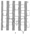
- Figure 1 depicts schematically a top view on a wafer showing the layout of active areas 110, wherein the active areas 110 are formed from the original wafer material Si. These active areas are embedded in a shallow trench isolation (STI) 100 formed from any suitable insulating material, which typically is silicon oxide SiO2. In this processing stage the STI 100 forms a planar surface, which will serve as a horizontal reference throughout the following description. Actually, the active areas 110 are covered by gate oxide, which is not shown here. However reference sign 110 shows the contour and location of the active areas 110.
- STI shallow trench isolation
- the active areas are arranged in a staggered manner.
- the active areas of adjacent columns are staggered by one half of the periodicity of the active areas in a column.
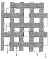
- Figure 2 depicts a view on the wafer after transistor gates have been formed as lines, such that a pair of parallel lines runs across a plurality of active areas 110.
- a suitable insulating layer which can be silicon nitride SiN or any other suitable insulating material covers the lines forming the transistor gates. Consequently in this view the insulating covers 200 upon the lines are visible, whereas the gate lines are hidden below the covers 200.
- Dotted line X-X' denotes the length and the direction of a cut line through the wafer, which in this figure runs into the paper plane.
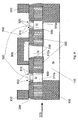
- Figure 3 depicts a cross sectional view along the cut line X-X' as shown in Fig. 2 .
- the arrow denoted by reference numeral 310 denotes the surface of the wafer serving as a reference plane, wherein the surface is the top surface of the STI 100.
- the active area 110 is embedded into the STI 100 and also covered by a thin layer of SiO2 material.
- Two parallel gate lines 320 each forming one transistor gate when running across the active area 110, run across the active area 110.
- the gate lines 320 are electrically insulated from the active area 110 by the thin layer of insulating material, which thus forms a gate dielectric.
- the material of the gate lines can be poly silicon or any other suitable conducting material or a stack of different layers, for example a stack of poly silicon below a suitable metal such as tungsten (W) and an insulating top layer such as silicon nitride SiN.
- each of the gate lines 320 serves as a gate for one selection transistor, thus the area denoted by reference numeral 110 will actually form two active areas of two respective, adjacent selection transistors.
- the two transistors will have a common source, which will be formed in later processing steps.
- the drains of the transistors are at the right hand end and at the left hand end respectively of area 110.
- Reference numerals 340, 341 thus denote the pathway of the current through the active area of a first and a second transistor respectively.
- the gate lines 320 are covered by a layer of insulating material 200.
- the sidewalls of the gate lines 320 are covered by insulating spacers 330, which have been produced by depositing a layer of suitable insulating material, preferably the same material, e.g. SiN, as used for the covering layer, and subsequent anisotropic etching. According to the anisotropic etching the bottom region of a spacer is thicker than the top region of a spacer.
- Source/Drain formation (not shown in the figures) with LDD (Low Density Drain) structure is performed by standard ion-implantation processes well known to those skilled in the art.
- a liner of a suitable insulating material e.g. SiN, can be deposited optionally, in order to protect the active areas in subsequent etching steps.
- arrow 350 denotes the distance between two gate lines 320, which can be 65 nanometers in this embodiment. Accordingly half-pitch size is 65 nanometers.
- interlayer dielectric for example such as silicon oxide (SiO) is deposited.
- SiO silicon oxide
- CMP chemical-mechanical polishing
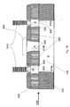
- Figure 4 depicts a top view on the surface of the wafer, wherein the ILD is omitted, as it would otherwise hide the structure, and showing stripes of a photo resist 410 positioned on the wafer.
- the stripes have been produced by a conventional processing, for example by depositing a layer photo resist on the entire wafer surface and subsequent lithographic steps and etching. Subsequently the ILD material is removed by etching, wherein due to the photo resist the ILD is maintained under the stripes.
- silicon is deposited on the structure, for example by using a chemical vapor deposition (CVD), such that gaps between the ILD under the stripes 410 and the gate lines 320 are filled. Said layer of silicon is then planarized by conventional CMP processing with reference to the top of the gate line covers 200.
- CVD chemical vapor deposition
- Figure 5 depicts a cross sectional view along cut line X-X' after depositing and planarizing the just deposited layer of silicon. In this way the gaps between the gate lines are filled with silicon, denoted by reference numerals 510a, 510b and 510c, wherein 510a and 510c will each serve as a drain contact for a transistor having 510b as a common source.
- Figure 6 shows a top view onto the surface of the structure after depositing and structuring a layer of photo resist 610 in order to protect the areas where the bit line contacts will be produced in the next processing steps.
- Said memory elements contacts will be produced on the silicon 510 deposited between the gate line stacks and the ILD. Accordingly the memory cells will be produced on the silicon 510.
- the silicon 510 is etched selectively in order to recess it.
- Fig. 7 depicts a cross sectional view as shown in Fig. 5 , but after performing the above mentioned processing steps of forming the photo resist stripes and subsequent selective etching of silicon, which can be a dry, chemical, for example a reactive ion etching (rie) process.
- the selective etching of the silicon causes the recession of the silicon 510 not covered by a photo resist layer. Accordingly the silicon 510a and 510 c are recessed, as they are not covered, whereas the silicon 510b is maintained without change. This etching process is performed until the height of the silicon 510a and 510c is recessed significantly, so as to provide an increasing opening above said silicon areas 510a and 510c.
- Figure 8 shows the cross sectional view of Fig. 7 after removal of the stripes of photo resist, which can be achieved by a conventional oxygen plasma processing, and producing spacers 810 on top of the silicon 510a and 510c and - horizontally - between the insulating spacers 330.
- These spacers 810 can be formed from any suitable material such as SiO 2 or SiN by a conventional process as described above for the insulating spacers 330.
- silicon 820 is epitactically grown on the silicon 510a and 510c to an extend so as to nearly fill the remaining gap between the spacers 810. Also silicon 830 is grown on the silicon 510b. Subsequently a salicidation with cobalt silicon (CoSi) or nickel silicon (NiSi) is performed to reduce contact resistances. As the salicidation takes place on the silicon surfaces only, the salicidation is self-aligned.
- CoSi cobalt silicon
- NiSi nickel silicon
- Figure 9 schematically depicts the cross sectional view after a layer of photo resist has been deposited on the structure, in particular in the form of stripes 910, which in this view are running into the paper plane, covering the structure where the bit line contacts will be formed, and with the exception of the area around the spacers 810 and the silicon 820, which will be the area of contacting the memory cells, in particular the area to form a contact for coupling to a volume of switching active material.
- a diluted hydrogen-fluoride (HF) dip is performed to recess the spacers 810, such that small chasms 920 are formed between the silicon 820 and the spacers 810.
- HF hydrogen-fluoride
- a suitable catalyst 930 for forming a nanowire or nanofiber or nanotube is deposited on the silicided areas 820.
- the catalyst can be a silicide forming metal, for example Ti, Pd, Pt, Au, Cu, Co, Cr, Hf, Ir, Mn, Mo, Ni, Rh, Ta, W, Zr, which can be deposited for example by an selective electroless deposition method, such that the catalyst is deposited on the silicided areas 820 only, as known e.g. from US 6,787,450 .
- any catalyst suitable for starting to grow a nanotube or nanowire or nanofiber can be used using any suitable deposition method.
- FIG. 10 The next processing steps are illustrated in Figure 10 , wherein the photo resist has been removed by using a conventional process. Furthermore the catalyst has been heated for coagulation thus scaling down the base area of the catalyst before a nanowire 1010 has been grown on the catalyst.
- the growth of the nanowire 1010 can be performed for example by a method described in " Nanowire Superlattices" by Charles M. Lieber in NANO LETTERS, Vol. 2 No.
- the nanowire 1010 is non-conducting or semi-conducting. Although any non-conducting material such as any non-conducting silicon derivate like SiN can be used, an intrinsic silicon nanowire is preferred.
- the nanowire has a diameter of 30 nanometers and a height of 50 to 200 nanometers.
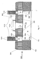
- Figure 11 depicts the cross sectional view along cut line X-X' after a nanotube 1110 of conducting material has been formed around the nanowires 1010. That is the nanowires 1010 have been used as a shaping die or mould for producing the nanotubes 1110 by depositing a liner of the conducting material, which at first covers the entire surface of the chip. Subsequently an anisotropic spacer etch is performed, which removes the conducting material from any horizontal surface, but substantially leaves the material at vertical surfaces, such that as a result the tubes are produced. In this way tubes 1110 of conducting material have been produced around the nanowires 1010. According to the direction of the nanowires, the rotation-axis of the tubes is perpendicular to the reference plane.
- the conducting material of the nanotubes can be any suitable conducting material, preferably titanium nitride (TiN), which can be deposited by a chemical vapor deposition (CVD) or an atomic layer deposition (ALD) process, which provide a good control of the thickness of the deposited layer.
- TiN titanium nitride
- CVD chemical vapor deposition
- ALD atomic layer deposition
- the thickness of the deposited TiN layer is less than 10 nanometers, preferably less than 5 nanometers and in particular below 2 nanometers.
- the chasms between the spacers 810 and the silicon 820 and the catalyst 930 respectively have been filled with the conducting material of the nanotubes.
- the nanotubes 1110 have a good electrical connection to the silicon 820 and 510a, 510c, wherein 510a is - as mentioned above - the drain of a first transistor and 510c is the drain of a second selection transistor respectively. Consequently the tubes 1110 are coupled to the drain of a first and a second transistor respectively.
- each nanotube 1110 forms a contact to the drain of a transistor and will be used, as will become clear later, as a contact to a volume of phase change material.
- spacers 1120 of the conducting material have been formed at the sidewalls of silicon 830. These spacers have not been formed intentionally but as a side effect when depositing the TiN layer and are left without any further treatment, as they do neither fulfill a specific purpose nor bother.
- Figure 12 shows a top view on the surface of the chip illustrating the layout after nanowires 1010 and the ring-shaped contacts, namely the nanotubes 1110 have been formed. Further on the spacers 1120 arranged around the blocks of silicon 830, 830 are shown, onto which the bitlines will be formed in later processing steps.
- an interlayer dielectric (ILD) 1310 is deposited on the structure, which is planarized by a conventional method, e.g. a CMP processing, wherein the planarization stops at the top of the nanotubes 1110 and the nanowires 1010 respectively.
- a conventional method e.g. a CMP processing
- the ILD covers the entire structure with the exception of the nanowires 1010 surrounded by the ring-shaped contacts - the nanotubes - 1110. Accordingly in a top view only the nanowires 1010 surround by the nanotubes 1110 embedded in the interlayer dielectric 1310 would be visible.
- the cross sectional view shows the volumes of switching active material 1320 contacting the ring-shaped front faces of the nanotubes 1110.
- the titanium nitride of the ring-shaped contacts and the material of the nanowires 1010 which can be intrinsic silicon, is selectively etched, to form a recess in the surface of the structure above every ring-shaped contact 1110.
- the bottom of the recess is thus formed by the nanowire 1010 and the ring-shaped front face of a nanotube 1110.
- the switching active material is deposited on the structure for filling the recesses.
- the switching active material which may be any conventional switching active material, preferably phase change material, can be deposited by any conventional process.
- the surface of the chip is again planarized using a conventional processing method, e.g. CMP, in order to remove the surplus of phase change material, which was not deposited in a recess, but on the surface structure.
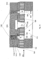
- Figure 14 depicts the cross sectional view after further processing in order to couple the volume of switching active material 1320 to a wordline.
- the stripe 1410 as well as its insulating cover 1420 are running into the paper plane. They have be formed using conventional method steps, namely by depositing the layers and subsequent lithographic and etch processing.
- insulating spacers 1430 of any suitable insulating material preferably of the same material as the insulating cover 1420, are produced at the sidewalls of the stack of 1410 and 1420 so as to insulate the sidewalls of the stripe of tungsten.
- These spacers can be formed conventionally as described above with respect to forming the spacers 330 at the sidewalls of the gate lines 320.
- interlayer dielectric 1440 of any suitable insulating material for example silicon oxide SiO, is deposited on the structure by any conventional method and planarized with respect to the top of the insulating cover 1420.
- a bitline contact 1450 is formed by etching a via into the interlayer dielectric layers 1440 and 1310 by using conventional lithographic processing and etching, wherein the etching is selective to the material of the insulating cover 1420 and spacers 1430, so that even in the case of a huge misalignment from the ideal position the insulating cover 1420 and the spacers 1430 remain without damage.
- a suitable conducting material for example tungsten (W)
- W tungsten
- TiN titanium nitride
- a liner of titanium nitride (TiN) is deposited on the walls of the via before it is filled with tungsten, in particular on the ground of the via in order to prevent the tungsten, that will be used for filling the via, from reacting with the silicon 510b.
- the TiN layer thus serves as a protective coating for the silicon of 510b.
- bitline 1460 is formed on the structure, wherein the shown bitline exemplifies a plurality of bitlines positioned in front of and behind the paper plane of the drawing and wherein each bitline couples a plurality of bitline contacts 1450.
- the bitline 1460 is running parallel to the paper plane and coupling to further bitline contacts 1450 of adjacent memory cells.
- the gate lines 320 serve as word lines
- bit lines 1460 are arranged orthogonal to the word lines.
- the bit lines 1460 can be formed by conventional processing steps, namely by depositing a layer of a suitable conducting material and subsequent lithographic processing and etching steps.
- Each memory cell comprises a volume of switching active material 1320 and a selection transistor for selecting one memory cell from the plurality of cells.
- the front face of a nanotube 1110 as described in the embodiment the bottom electrode contact, forms one electrode contacting the volume of the switching active material 1320.
- the nanotubes have been produced by first forming nanowires 1010, which subsequently served as a mould for forming nanotubes 1110. As the nanotubes 1110 are contacting the drain of a selection transistor, the volumes of switching active material 1320 are coupled to the drain of a selection transistor via a conducting nanotube.
- selection elements like diodes can be used instead of a selection transistor.
- vertical diodes more specifically vertical pn diodes as a selection element. To fabricate such vertical diodes, an array of heavily n+ doped active area silicon lines separated by STI regions are formed constituting the word lines. After depositing an ILD layer (e.g.
- contact holes are formed by conventional litho and etch processing, opening parts of the heavily n+ doped active area.
- single-crystal silicon can be grown by selective epitaxial growth with CVD method on the opened n+ doped active area regions to fill the contact holes.
- the vertical pn diode is formed inside the contact holes by two sequential ion implantation steps (a first deep n+ implant followed by a shallow p+ implant).
- the fabrication of the switching active elements can be continued as already described in the other preferred embodiments.
- a heating current for heating the volume or only a part of the volume of switching active material 1320 will flow through bit line 1460 and through bit line contact 1450 into the silicon 510b, which can be seen as a source of the two adjacent transistors.
- bit line 1460 In case that one - or both - of the gate lines 320 has a suitable potential then a conducting channel will be produced in the active area 110.
- the current correspondingly will flow through 510 to either 510a or 510c - or both- and further to 930. From thereon the current will flow through the sidewalls of 930 into a tube 1110, which forms a bottom electrode contact of a volume of switching active material 1320.
- the current will leave the switching active material through a top electrode contact 1410 which also forms the ground or reference electrode having ground or a reference potential, and which runs into the paper plane in this view.
- Figure 15 depicts a top view onto the structure showing the layout. Although in the drawing each of the bit lines 1460 is coupled to only one bit line contact 1450, each bit line 1460 is coupled to a plurality of bit line contacts 1450 and thus to a plurality of memory cells, in bit line direction, wherein the other bit line contacts are not shown in this top view. Each bit line 1460 is further coupled to logic - not shown - for sensing the voltage or current level of the bit line.
- a further layer of interlayer dielectric filling the gaps between the bit lines 1460 is omitted in this view, as otherwise the layers below would be invisible in this view.
- bit line contacts 1450 are circumferentially embedded in non-conducting inter layer dielectric 1440.
Landscapes
- Engineering & Computer Science (AREA)
- Chemical & Material Sciences (AREA)
- Crystallography & Structural Chemistry (AREA)
- Computer Hardware Design (AREA)
- Manufacturing & Machinery (AREA)
- Semiconductor Memories (AREA)
- Internal Circuitry In Semiconductor Integrated Circuit Devices (AREA)
Applications Claiming Priority (1)
| Application Number | Priority Date | Filing Date | Title |
|---|---|---|---|
| US11/640,065 US8188569B2 (en) | 2006-12-15 | 2006-12-15 | Phase change random access memory device with transistor, and method for fabricating a memory device |
Publications (1)
| Publication Number | Publication Date |
|---|---|
| EP1933382A2 true EP1933382A2 (de) | 2008-06-18 |
Family
ID=39125195
Family Applications (1)
| Application Number | Title | Priority Date | Filing Date |
|---|---|---|---|
| EP07021307A Withdrawn EP1933382A2 (de) | 2006-12-15 | 2007-10-31 | Phasenwechsel-RAM-Speichervorrichtung mit Transistor und Verfahren zur Herstellung einer Speichervorrichtung |
Country Status (5)
| Country | Link |
|---|---|
| US (1) | US8188569B2 (de) |
| EP (1) | EP1933382A2 (de) |
| JP (1) | JP2008172218A (de) |
| KR (1) | KR20080056090A (de) |
| CN (1) | CN101207149A (de) |
Families Citing this family (18)
| Publication number | Priority date | Publication date | Assignee | Title |
|---|---|---|---|---|
| US20080265234A1 (en) * | 2007-04-30 | 2008-10-30 | Breitwisch Matthew J | Method of Forming Phase Change Memory Cell With Reduced Switchable Volume |
| US8283786B2 (en) * | 2007-12-21 | 2012-10-09 | Advanced Micro Devices, Inc. | Integrated circuit system with contact integration |
| US8558220B2 (en) * | 2007-12-31 | 2013-10-15 | Sandisk 3D Llc | Memory cell that employs a selectively fabricated carbon nano-tube reversible resistance-switching element formed over a bottom conductor and methods of forming the same |
| US8878235B2 (en) | 2007-12-31 | 2014-11-04 | Sandisk 3D Llc | Memory cell that employs a selectively fabricated carbon nano-tube reversible resistance-switching element and methods of forming the same |
| US8530318B2 (en) * | 2008-04-11 | 2013-09-10 | Sandisk 3D Llc | Memory cell that employs a selectively fabricated carbon nano-tube reversible resistance-switching element formed over a bottom conductor and methods of forming the same |
| US20090257264A1 (en) * | 2008-04-11 | 2009-10-15 | Heinz Hoenigschmid | Memory and method of evaluating a memory state of a resistive memory cell |
| KR100968449B1 (ko) * | 2008-05-27 | 2010-07-07 | 주식회사 하이닉스반도체 | 고집적 상변화 메모리 장치 및 그 제조방법 |
| KR101429724B1 (ko) * | 2008-12-10 | 2014-08-13 | 삼성전자주식회사 | 콘택 구조체 형성방법, 이를 이용하는 반도체소자의 제조방법 및 그에 의해 제조된 반도체소자 |
| KR101565797B1 (ko) * | 2009-02-16 | 2015-11-05 | 삼성전자주식회사 | 콘택 플러그를 포함하는 반도체 장치 |
| US8058095B2 (en) | 2009-06-23 | 2011-11-15 | Micron Technology, Inc. | Encapsulated phase change cell structures and methods |
| US8574954B2 (en) | 2010-08-31 | 2013-11-05 | Micron Technology, Inc. | Phase change memory structures and methods |
| US9564447B1 (en) * | 2015-09-01 | 2017-02-07 | Globalfoundries Inc. | Methods for fabricating programmable devices and related structures |
| US9865655B2 (en) * | 2015-12-15 | 2018-01-09 | Taiwan Semiconductor Manufacturing Co., Ltd. | Memory cell structure with resistance-change material and method for forming the same |
| CN110945656B (zh) * | 2017-08-17 | 2024-05-24 | 英特尔公司 | 晶体管制造中的集成的纳米线及纳米带图案化 |
| CN113948476B (zh) | 2020-07-16 | 2025-01-14 | 长鑫存储技术有限公司 | 半导体结构及其制备方法 |
| US11895821B2 (en) | 2020-07-16 | 2024-02-06 | Changxin Memory Technologies, Inc. | Semiconductor structure and manufacturing method thereof |
| US11653581B2 (en) | 2020-08-13 | 2023-05-16 | Taiwan Semiconductor Manufacturing Co., Ltd. | RRAM device structure and manufacturing method |
| CN113121235B (zh) * | 2021-04-09 | 2022-04-12 | 哈尔滨工业大学 | 一种温差发电材料的制备方法 |
Family Cites Families (14)
| Publication number | Priority date | Publication date | Assignee | Title |
|---|---|---|---|---|
| US6969866B1 (en) * | 1997-10-01 | 2005-11-29 | Ovonyx, Inc. | Electrically programmable memory element with improved contacts |
| US6312304B1 (en) * | 1998-12-15 | 2001-11-06 | E Ink Corporation | Assembly of microencapsulated electronic displays |
| JP4558950B2 (ja) * | 1999-03-25 | 2010-10-06 | オヴォニクス インコーポレイテッド | 改善された接合を有する電気的にプログラム可能なメモリ素子 |
| US6611039B2 (en) * | 2001-09-28 | 2003-08-26 | Hewlett-Packard Development Company, L.P. | Vertically oriented nano-fuse and nano-resistor circuit elements |
| KR100437458B1 (ko) * | 2002-05-07 | 2004-06-23 | 삼성전자주식회사 | 상변화 기억 셀들 및 그 제조방법들 |
| US6787450B2 (en) * | 2002-05-29 | 2004-09-07 | Micron Technology, Inc. | High aspect ratio fill method and resulting structure |
| KR100982419B1 (ko) * | 2003-05-01 | 2010-09-15 | 삼성전자주식회사 | 탄소나노튜브를 이용한 반도체 소자의 배선 형성 방법 및이 방법에 의해 제조된 반도체 소자 |
| US7291556B2 (en) * | 2003-12-12 | 2007-11-06 | Samsung Electronics Co., Ltd. | Method for forming small features in microelectronic devices using sacrificial layers |
| WO2006003620A1 (en) * | 2004-06-30 | 2006-01-12 | Koninklijke Philips Electronics N.V. | Method for manufacturing an electric device with a layer of conductive material contacted by nanowire |
| US7323730B2 (en) * | 2004-07-21 | 2008-01-29 | Commissariat A L'energie Atomique | Optically-configurable nanotube or nanowire semiconductor device |
| US20060034116A1 (en) * | 2004-08-13 | 2006-02-16 | Lam Chung H | Cross point array cell with series connected semiconductor diode and phase change storage media |
| DE102005014645B4 (de) * | 2005-03-31 | 2007-07-26 | Infineon Technologies Ag | Anschlusselektrode für Phasen-Wechsel-Material, zugehöriges Phasen-Wechsel-Speicherelement sowie zugehöriges Herstellungsverfahren |
| KR100707190B1 (ko) * | 2005-05-07 | 2007-04-13 | 삼성전자주식회사 | 나노 와이어를 포함하는 상변환 메모리 소자 및 그 제조방법 |
| US7420199B2 (en) * | 2005-07-14 | 2008-09-02 | Infineon Technologies Ag | Resistivity changing memory cell having nanowire electrode |
-
2006
- 2006-12-15 US US11/640,065 patent/US8188569B2/en not_active Expired - Fee Related
-
2007
- 2007-10-31 EP EP07021307A patent/EP1933382A2/de not_active Withdrawn
- 2007-11-23 CN CNA2007101877542A patent/CN101207149A/zh active Pending
- 2007-12-13 KR KR1020070129966A patent/KR20080056090A/ko not_active Ceased
- 2007-12-14 JP JP2007323805A patent/JP2008172218A/ja active Pending
Also Published As
| Publication number | Publication date |
|---|---|
| US20080142776A1 (en) | 2008-06-19 |
| JP2008172218A (ja) | 2008-07-24 |
| CN101207149A (zh) | 2008-06-25 |
| KR20080056090A (ko) | 2008-06-20 |
| US8188569B2 (en) | 2012-05-29 |
Similar Documents
| Publication | Publication Date | Title |
|---|---|---|
| EP1933382A2 (de) | Phasenwechsel-RAM-Speichervorrichtung mit Transistor und Verfahren zur Herstellung einer Speichervorrichtung | |
| US6943365B2 (en) | Electrically programmable memory element with reduced area of contact and method for making same | |
| US8039372B2 (en) | Methods of manufacturing variable resistance non-volatile memory devices including a uniformly narrow contact layer | |
| US7696508B2 (en) | Phase change memory devices having dual lower electrodes | |
| CN102237390B (zh) | 半导体装置及其制造方法 | |
| US20120007031A1 (en) | Phase change memory cell with heater and method therefor | |
| WO2015038246A2 (en) | Method of integrating select gate source and memory hole for three-dimensional non-volatile memory device | |
| WO2015041743A1 (en) | High aspect ratio memory hole channel contact formation | |
| KR20070115707A (ko) | 메모리 디바이스, 특히 트랜지스터를 갖는 상 변화 랜덤액세스 메모리, 및 메모리 디바이스를 제조하는 방법 | |
| CN110600499A (zh) | 高密度电阻性随机存取存储器(rram) | |
| US7989795B2 (en) | Phase change memory device and method for fabricating the same | |
| CN101483185B (zh) | 存储器单元和存储器阵列 | |
| TW201135873A (en) | A memory cell that includes a carbon-based memory element and methods of forming the same | |
| US9177995B2 (en) | Vertical interconnect structure, memory device and associated production method | |
| US8043924B2 (en) | Methods of forming phase-change memory units, and methods of manufacturing phase-change memory devices using the same | |
| US7745809B1 (en) | Ultra high density phase change memory having improved emitter contacts, improved GST cell reliability and highly matched UHD GST cells using column mirco-trench strips | |
| US9076866B2 (en) | Semiconductor device and method for fabricating the same | |
| US20110108792A1 (en) | Single Crystal Phase Change Material | |
| CN114270514B (zh) | 制造具有垂直的预定灯丝的电阻式存储器的结构和方法 | |
| US20230160944A1 (en) | Reliability Macros for Contact Over Active Gate Layout Designs | |
| US20240268115A1 (en) | Three-dimensional memory device containing heterojunction source layer and method for manufacturing the same | |
| US20260123294A1 (en) | Phase change material device and methods for forming the same | |
| KR20090084218A (ko) | 가변 저항 메모리 장치 | |
| KR20260054621A (ko) | 측벽 라이너를 사용하는 상 변화 재료 디바이스 및 그 형성 방법들 | |
| WO2025014569A1 (en) | Three-dimensional memory device including horizontal semiconductor channels and methods of forming the same |
Legal Events
| Date | Code | Title | Description |
|---|---|---|---|
| PUAI | Public reference made under article 153(3) epc to a published international application that has entered the european phase |
Free format text: ORIGINAL CODE: 0009012 |
|
| AK | Designated contracting states |
Kind code of ref document: A2 Designated state(s): AT BE BG CH CY CZ DE DK EE ES FI FR GB GR HU IE IS IT LI LT LU LV MC MT NL PL PT RO SE SI SK TR |
|
| AX | Request for extension of the european patent |
Extension state: AL BA HR MK RS |
|
| 19U | Interruption of proceedings before grant |
Effective date: 20090401 |
|
| 19W | Proceedings resumed before grant after interruption of proceedings |
Effective date: 20091123 |
|
| STAA | Information on the status of an ep patent application or granted ep patent |
Free format text: STATUS: THE APPLICATION IS DEEMED TO BE WITHDRAWN |
|
| 18D | Application deemed to be withdrawn |
Effective date: 20100526 |