EP1933294A2 - Bildanzeigevorrichtung und Antriebsverfahren für die Bildanzeigevorrichtung - Google Patents
Bildanzeigevorrichtung und Antriebsverfahren für die Bildanzeigevorrichtung Download PDFInfo
- Publication number
- EP1933294A2 EP1933294A2 EP07122812A EP07122812A EP1933294A2 EP 1933294 A2 EP1933294 A2 EP 1933294A2 EP 07122812 A EP07122812 A EP 07122812A EP 07122812 A EP07122812 A EP 07122812A EP 1933294 A2 EP1933294 A2 EP 1933294A2
- Authority
- EP
- European Patent Office
- Prior art keywords
- pixel
- data
- modulation signal
- pixels
- luminance
- Prior art date
- Legal status (The legal status is an assumption and is not a legal conclusion. Google has not performed a legal analysis and makes no representation as to the accuracy of the status listed.)
- Withdrawn
Links
Images






Classifications
-
- G—PHYSICS
- G09—EDUCATION; CRYPTOGRAPHY; DISPLAY; ADVERTISING; SEALS
- G09G—ARRANGEMENTS OR CIRCUITS FOR CONTROL OF INDICATING DEVICES USING STATIC MEANS TO PRESENT VARIABLE INFORMATION
- G09G3/00—Control arrangements or circuits, of interest only in connection with visual indicators other than cathode-ray tubes
- G09G3/20—Control arrangements or circuits, of interest only in connection with visual indicators other than cathode-ray tubes for presentation of an assembly of a number of characters, e.g. a page, by composing the assembly by combination of individual elements arranged in a matrix no fixed position being assigned to or needed to be assigned to the individual characters or partial characters
- G09G3/22—Control arrangements or circuits, of interest only in connection with visual indicators other than cathode-ray tubes for presentation of an assembly of a number of characters, e.g. a page, by composing the assembly by combination of individual elements arranged in a matrix no fixed position being assigned to or needed to be assigned to the individual characters or partial characters using controlled light sources
-
- G—PHYSICS
- G09—EDUCATION; CRYPTOGRAPHY; DISPLAY; ADVERTISING; SEALS
- G09G—ARRANGEMENTS OR CIRCUITS FOR CONTROL OF INDICATING DEVICES USING STATIC MEANS TO PRESENT VARIABLE INFORMATION
- G09G3/00—Control arrangements or circuits, of interest only in connection with visual indicators other than cathode-ray tubes
- G09G3/20—Control arrangements or circuits, of interest only in connection with visual indicators other than cathode-ray tubes for presentation of an assembly of a number of characters, e.g. a page, by composing the assembly by combination of individual elements arranged in a matrix no fixed position being assigned to or needed to be assigned to the individual characters or partial characters
- G09G3/2007—Display of intermediate tones
- G09G3/2014—Display of intermediate tones by modulation of the duration of a single pulse during which the logic level remains constant
-
- G—PHYSICS
- G09—EDUCATION; CRYPTOGRAPHY; DISPLAY; ADVERTISING; SEALS
- G09G—ARRANGEMENTS OR CIRCUITS FOR CONTROL OF INDICATING DEVICES USING STATIC MEANS TO PRESENT VARIABLE INFORMATION
- G09G2320/00—Control of display operating conditions
- G09G2320/02—Improving the quality of display appearance
- G09G2320/0223—Compensation for problems related to R-C delay and attenuation in electrodes of matrix panels, e.g. in gate electrodes or on-substrate video signal electrodes
-
- G—PHYSICS
- G09—EDUCATION; CRYPTOGRAPHY; DISPLAY; ADVERTISING; SEALS
- G09G—ARRANGEMENTS OR CIRCUITS FOR CONTROL OF INDICATING DEVICES USING STATIC MEANS TO PRESENT VARIABLE INFORMATION
- G09G2320/00—Control of display operating conditions
- G09G2320/04—Maintaining the quality of display appearance
- G09G2320/043—Preventing or counteracting the effects of ageing
-
- G—PHYSICS
- G09—EDUCATION; CRYPTOGRAPHY; DISPLAY; ADVERTISING; SEALS
- G09G—ARRANGEMENTS OR CIRCUITS FOR CONTROL OF INDICATING DEVICES USING STATIC MEANS TO PRESENT VARIABLE INFORMATION
- G09G2320/00—Control of display operating conditions
- G09G2320/04—Maintaining the quality of display appearance
- G09G2320/043—Preventing or counteracting the effects of ageing
- G09G2320/048—Preventing or counteracting the effects of ageing using evaluation of the usage time
-
- G—PHYSICS
- G09—EDUCATION; CRYPTOGRAPHY; DISPLAY; ADVERTISING; SEALS
- G09G—ARRANGEMENTS OR CIRCUITS FOR CONTROL OF INDICATING DEVICES USING STATIC MEANS TO PRESENT VARIABLE INFORMATION
- G09G2360/00—Aspects of the architecture of display systems
- G09G2360/16—Calculation or use of calculated indices related to luminance levels in display data
Definitions
- the present invention relates to an image display apparatus and a driving method of the image display apparatus.
- JP-A Japanese Patent Application Laid-Open ( JP-A) No. 2-257553 discloses controlling of a pulse width of a voltage to be applied to each of modulation electrodes in order to compensate variation of the amount of electron-emitting beam from each of a plurality of electron-emitting devices due to variation of a voltage to be applied to each of the plurality of electron-emitting devices.
- JP-A No. 8-248920 discloses an image forming apparatus using electron-emitting devices that are arranged in a simple matrix.
- This image forming apparatus is provided with drive signal generating unit for outputting a drive pulse for driving a cold-cathode device to be connected to a selected row wiring to each of a plurality of column wirings.
- This drive signal generating unit outputs a drive pulse that is corrected by a correction value corresponding to each column wiring.
- JP-A No. 2003-223131 discloses a structure providing a plurality of reference positions in row wirings in order to make hardware for calculating a correction value small and obtaining a correction value for this.
- a quality of an image to be displayed is lowered if a signal loss such as a voltage drop takes place.
- a signal loss such as a voltage drop
- the present invention provides an image display apparatus having improved correction accuracy.
- the present invention in its first aspect provides an image display apparatus as specified in claim 1.
- the present invention in its second aspect provides a driving method of an image display apparatus as specified in claim 2.
- the present invention in its third aspect provides an image display apparatus as specified in claim 3.
- the present invention in its fourth aspect provides a driving method of an image display apparatus as specified in claim 4.
- the present invention in its fifth aspect provides an image display apparatus as specified in claims 5, and 7-11.
- the present invention in its sixth aspect provides a driving method of an image display apparatus as specified in claim 6.
- the present invention in its seventh aspect provides an image display apparatus as specified in claims 12 and 14.
- the present invention in its eighth aspect provides a driving method of an image display apparatus as specified in claim 13.
- the present invention can be preferably applied to a display apparatus for displaying an image while driving a plurality of pixels.
- the present invention can be preferably applied to a display apparatus that is configured so that a loss of a signal to be provided to a predetermined pixel affects the lighting state of other pixel.
- a loss of a signal to be provided to a predetermined pixel affects the lighting state of other pixel.
- the lighting state of each pixel is affected by the lighting state of other pixels.
- a configuration such that a plurality of pixels are driven in a matrix by a plurality of scan signal wirings (each of the scan signal wirings is equivalent to a common wiring) and a plurality of modulation signal wirings in a line-sequence.
- the pixels are driven.
- a signal level on the scan signal wiring is different depending on a position on the scan signal wiring because a voltage drop takes place when an electric current flows through the scan signal wiring. Accordingly, the voltage drop becomes large on the position far from the position where the scan signal is applied. In other words, the signal loss becomes large.
- the value of the electric current flowing through the scan signal wiring is decided by the driving state of each pixel.
- the driving state of each pixel is decided by the data to indicate the luminance of each pixel, for example, luminance data, so that the signal loss depends not only on a distance from the position where the signal is applied but also an image to be displayed.
- a pixel that is formed by combining a pixel circuit using a device such as a TFT for controlling the voltage to be applied with a liquid crystal, and a pixel that is formed by combining a pixel circuit using a device such as a TFT for controlling an electric current to be supplied to an EL material with the EL material.
- a sub pixel is not particularly distinguished from “a pixel” formed by combining a plurality of "sub pixels”. Accordingly, the present invention does not exclude the configuration such that "the pixel” defined by the present invention is used as "the sub pixel” in the configuration that one pixel is formed by combining the sub pixels having plural different colors.
- the pixel formed by combining the electron-emitting device and a light-emitting member that emits light when electrons to be emitted from the electron-emitting device are irradiated thereto is used.
- An example of an image display apparatus having a display panel for driving a plurality of electron-emitting devices in a simple matrix is shown below.
- the electron-emitting devices on the selected row wiring are turned on electricity.
- the current to be turned on flows through the same row wiring, the current is concentrated on the row wiring and this generates a voltage drop.
- the configuration that the surface conduction electron-emitting device is used as the electron-emitting device is illustrated by an example below. Since the surface conduction electron-emitting device is characterized in that large amounts of currents flow through the row wiring and a voltage drop amount is large, particularly, the present invention can be preferably applied to the surface conduction electron-emitting device.
- an image display apparatus having a display panel having the surface conduction electron-emitting devices connected in a simple matrix and a correction circuit for outputting corrected image data on the basis of inputted image data or the like
- a drive circuit according to the present embodiment, an example using the drive circuit for driving the row wiring in a line-sequence and applying the modulation pulse which is modulated at least a pulse width thereof to the column wiring will be described.
- the lighting time of each pixel is controlled by a pulse width modulation (PWM).
- PWM pulse width modulation
- a pulse height modulation is also carried out together with control of the lighting time by the pulse width modulation and a lighting intensity within a lighting time is controlled by a pulse height modulation, so that the number of tones that can be modulated may be increased.
- PLM pulse height modulation
- the image display apparatus can display a preferable image. Further, the influence of the voltage drop in the pulse width modulation is described in columns 0084 to 0095 of JP-A No. 2003-223131 (columns [0095] to [0107] of US2003/0006976A1 ).
- FIG. 2 is a block diagram of the image display apparatus according to the present embodiment.
- the image display apparatus includes an inverse ⁇ conversion unit 201, a corrected image data calculation circuit 202, a modulation circuit 203 that is a modulation signal output circuit, a scan circuit 204, a display panel 205, a high voltage electric source 206, a timing generation circuit 207, and a surface conduction electron-emitting device 208.
- the image display apparatus may be operated on the basis of a timing signal generated by the timing generation circuit 207 with reference to a horizontal synchronization HD and a vertical synchronization VD of the picture signal.
- the image data Data are inputted in the inverse ⁇ conversion unit 201.
- the image data Data are represented as "Data" in FIG. 2 for simplification and they correspond to color picture signals R, G, and B, in color image display apparatus, respectively to be inputted in the inverse ⁇ conversion unit 201 in a point-sequence.
- the display panel 205 using the surface conduction electron-emitting device 208 has a property of emitting a light of luminance that is nearly linear for the application time of the pulse. Further, the pulse width modulation may modulate a time integration value of the luminance.
- the inverse ⁇ conversion unit 201 converts the image data Data using a curve of 2.2 powers so as to generate image data D1. Then, the inverse ⁇ conversion unit 201 provides the image data D1 having a value in proportion to the luminance to the corrected image data calculation circuit 202.
- the image data D1 corresponds to the data to indicate the luminance of the pixel.
- the corrected image data calculation circuit 202 outputs corrected image data D2 with reference to the image data D1.
- the corrected image data D2 corresponds to the data to determine the lighting time of the pixel.
- the modulation circuit 203 is connected to the column wiring that is the modulation signal wiring of the display panel 205.
- the corrected image data D2 is inputted from the corrected image data calculation circuit 202 in this modulation circuit 203 and timing data is inputted from the timing generation circuit 207 in this modulation circuit 203.
- the modulation circuit 203 generates a modulation signal in accordance with the inputted corrected image data D2. Specifically, counting a clock signal in the number of time that is indicated by the corrected image data D2, a time that is not turned off of the modulation signal (namely, a time that is turned on) is determined. One period of the clock signal is made into a unit time (a time slot) for controlling the lighting time of the pixel.
- the modulation circuit 203 outputs the modulation signal to the column wiring that is connected to each of a plurality of the surface conduction electron-emitting devices 208.
- the scan circuit 204 is connected to the row wiring that is the scan signal wiring of the display panel 205.
- the scan circuit 204 provides a selection signal (a scan signal) to the scan signal wiring to which the surface conduction electron-emitting devices 208 to be driven is connected.
- the scan circuit 204 carries out scanning in a line-sequence for selecting the scan signal wiring in sequence for each row.
- the present embodiment is not limited to this and the present embodiment may be configured so that the scan circuit 204 carries out interlace scanning or selects a plurality of rows at the same time.
- the scan circuit 204 selects a row by giving a selection electric potential for a predetermined time to the row wiring to which some surface conduction electron-emitting devices 208 that are target for driving among a plurality of surface conduction electron-emitting devices 208 included in the display panel 205.
- the scan circuit 204 does not select the row by giving a no-selection electric potential for a time other than the predetermined time to the row wiring.
- the timing generation circuit 207 generates a timing signal for the modulation circuit 203, the scan circuit 204, and the corrected image data calculation circuit 202.
- the display panel 205 includes an electron source to arrange a plurality of surface conduction electron-emitting devices 208 in its inside and a plurality of light-emitting members that are arranged so as to be opposite to the electron source.
- FIG. 13 is a typical view of a scan signal wiring that is a common wiring, a plurality of surface conduction electron-emitting devices to configure a plurality of pixels to be connected to the scan signal wiring, a plurality of modulation signal wirings, and a light-emitting member to configure a pixel.
- a pixel only for one row is described.
- One pixel (a first pixel) is configured by a surface conduction electron-emitting device 1304 that is an electron-emitting device and a phosphor 1306 that is a light-emitting member.
- One pixel (a second pixel) is configured by a surface conduction electron-emitting device 1305 that is an electron-emitting device and a phosphor 1307 that is a light-emitting member.
- the surface conduction electron-emitting devices 1304 and 1305 are connected to one common wiring (namely, a scan signal wiring 1301) in common. Accordingly, the first pixel and the second pixel are connected to one common wiring in common.
- the modulation signal is supplied to the first pixel by a modulation signal wiring 1302 and the modulation signal is supplied to the second pixel by a modulation signal wiring 1303.
- an electron to be emitted from the surface conduction electron-emitting device is irradiated to the light-emitting member arranged so as to be opposite to the electron source to generate a light. Due to this set of lights, an image is displayed.
- the luminance of the light is controlled by an irradiation amount of electrons from the surface conduction electron-emitting device.
- the irradiation amount of electrons from the surface conduction electron-emitting device is controlled by a volume of a voltage to be applied to the surface conduction electron-emitting device and an application time of the voltage.
- the electron source has a plurality of scan signal wirings and a plurality of modulation signal wirings so that a plurality of surface conduction electron-emitting devices 208 can be driven in a matrix. Applying a scan signal to this scan signal wiring, a modulation signal is applied to a modulation signal wiring.
- the high voltage electric source 206 provides a high voltage to the side of a light-emitting member in order to direct an electron emitted from the electron source to the light-emitting member.
- FIG. 1 is a schematic view showing the corrected image data calculation circuit 202 that is a correction circuit.
- the corrected image data calculation circuit 202 includes a lighting pattern calculation circuit 101, a voltage drop amount calculation circuit 102, an accumulation circuit (an accumulator) 103, a comparator 104, a register 105, and a shift register 106.
- a block formed by the voltage drop amount calculation circuit 102, the accumulation circuit 103, the comparator 104, and the register 105 is referred to as a luminance accumulation circuit 100.
- the top luminance accumulation circuit 100 in FIG. 1 corresponds to a first correction unit
- the second top luminance accumulation circuit 100 and the lighting pattern calculation circuit 101 in FIG. 1 correspond to a second correction unit.
- the luminance accumulation circuit 100 is provided for each wiring corresponding to each modulation signal wiring of the display panel 205.
- a timing controller 107 synchronizes the luminance accumulation circuit 100, the lighting pattern calculation circuit 101, the shift register 106, and a slot number counter 108.
- the timing controller 107 controls the operation of the luminance accumulation circuit 100 for each modulation signal wiring and the operation of the slot number counter to be described later. Specifically, by controlling clear and enable of the accumulator 103 and clear and enable of the slot number counter 108, timing for accumulating the luminance and time slots per modulation signal wiring are managed.
- the voltage drop amount calculation circuit 102 is a circuit for calculating luminance ⁇ L[I] in a modulation signal wiring I (column I) defining the lighting patterns of all modulation signal wirings as input.
- the luminance ⁇ L[I] is a value representing luminance within a predetermined period of time of the Ith pixel.
- the luminance ⁇ L[I] is calculated in response to each period of time, respectively. Further, it is not necessary to synchronize the calculation by the correction circuit with output of the modulation signal from the modulation signal output circuit and the calculation may be carried out without synchronization.
- the luminance ⁇ L to be calculated by the voltage drop amount calculation circuit 102 will be obtained as follows.
- the calculation will be carried out according to a Kirchhoff law in consideration of: a lighting pattern; output resistances of a scan signal wiring, a modulation signal wiring, the scan circuit 204, and the modulation circuit 203; and an I-V characteristic of the surface conduction electron-emitting device 208.
- a voltage drop amount (a signal loss amount) of each part of the scan signal wiring and a voltage to be applied to each surface conduction electron-emitting device are calculated.
- the emission current amount is estimated.
- the luminance ⁇ L to be stored in the voltage drop amount calculation circuit 102 is obtained.
- the slot number counter 108 counts the number of slots indicating how many times accumulation is made when accumulating the luminance in a sequence in synchronization with a slot. For example, the slot number counter 108 counts the number of slots "1" when the luminance is accumulated at the first timing and the slot number counter 108 counts the number of slots "2" when the luminance is accumulated at the second timing.
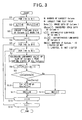
- FIG. 3 is a flow chart showing the operation of the corrected image data calculation circuit 202 of the image display apparatus according to the present embodiment.
- the flow chart in FIG. 3 is partially indicated in a sequence processing for convenience of description.
- the lighting pattern calculation circuit 101 is a circuit for creating a lighting pattern for a certain time. Further, the lighting pattern refers to the application state of the voltage to each modulation signal wiring. For example, in the case of lighting (turning ON) the all display devices connected to four modulation signal wirings, the lighting pattern is represented as (1, 1, 1, 1) ("1" means ON and "0" means OFF).
- the lighting pattern to be determined in the lighting pattern calculation circuit 101 is formed to be rewritten on the basis of a result of correction calculation. Further, practical application of a modulation signal is made after the calculation in this correction circuit is completed, so that on the stage of the correction calculation, the lighting having the result of the correction reflected is not carried out.
- the procedures will be described in sequence.
- the lighting pattern calculation circuit 101 creates the lighting patterns from the first modulation signal wiring 0 to a modulation signal wiring N - 1 on the basis of the image data D1.
- the lighting patterns are calculated (S1 to S4). Further, in a step S2, setting the accumulated luminance value (L[1]) in the scan signal wiring I at "0", a value of the corrected image data in the scan signal wiring I (CDdata[I]) is set at "0".
- the luminance accumulation circuit 100 calculates while counting the number of time slots from the first time slot 0 to the Mth time slot M - 1 (S5, S14).
- the M pieces of time slots correspond to M pieces of periods of time in a selection period (a period that a modulation signal can be outputted).
- M is defined to be a natural number not less than 2.
- Step S7 corresponds to the operation of the voltage drop amount calculation circuit 102 in FIG. 1 .
- Step S8 corresponds to the accumulation circuit 103 in FIG. 1 and step S9 corresponds to the comparator 104 in FIG. 1 .
- a plurality of luminance accumulation circuits 100 obtains the corrected image data for each modulation signal wiring by the parallel operation.
- the processing for obtaining the corrected image data is represented by loop processing (S6, S13) for convenience of description. In any of the serial processing by the loop calculation or the parallel processing using a plurality of circuit blocks, the present invention is practicable.
- the voltage drop amount calculation circuit 102 refers to a lighting pattern of all modulation signal wirings and calculates the luminance ⁇ L[I] in the modulation signal wiring I (S7).
- the voltage drop amount calculation circuit 102 calculates the luminance amount that is different for each modulation signal wiring even if referring to the same lighting pattern. It is because that the voltage drop amount in a row wiring direction is different for each modulation signal wiring.
- the luminance ⁇ L is an amount that is decided by the volume of the voltage drop on the scan signal wiring that is selected when the pixel is driven by the lighting pattern, a characteristic curve between the applied voltage and the emission current of the surface conduction electron-emitting device, and a characteristic of a phosphor that is placed on the display panel.
- the voltage drop amount calculation circuit 102 calculates the volume of the voltage drop for the lighting pattern for each time, however, a table that has been calculated in advance may be referred.
- the voltage drop amount calculation circuit 102 outputs the calculation result to the accumulation circuit 103.
- the luminance ⁇ L (namely, the value representing the luminance during this period of time) is calculated.
- the luminance ⁇ L is calculated.
- the accumulation circuit 103 in synchronization with a timing signal from the timing controller 107, accumulates the luminance ⁇ L[I] in sequence in accordance with counting up of the slot number counter 108 and outputs the accumulated luminance L (corresponding to "the accumulated value” according to the present invention) in sequence (S8). In other words, the accumulation circuit 103 outputs the luminance L in sequence by accumulating the value calculated by the voltage drop amount calculation circuit 102 (the luminance ⁇ L [I]) for each timing in sequence. In other words, the accumulation circuit 103 temporarily accumulates the value that is calculated by the voltage drop amount calculation circuit 102 so as to calculate the accumulated value. The accumulation circuit 103 accumulates the luminance ⁇ L of each period of time in sequence.
- the accumulation circuit 103 may be configured so as to stop the accumulation with respect to that pixel after that period of time.
- the accumulation circuit 103 outputs the accumulated luminance L to the comparator 104.
- the comparator 104 compares the Data [I] of the image data D1 corresponding to each modulation signal wiring (corresponding to a value of the data to indicate the luminance of the pixel) with the accumulated luminance L[I], whenever the luminance ⁇ L[I] during each period of time is calculated and further added to the accumulated value from the first period of time to the former period of time (S9).
- the value obtained by accumulating the luminance ⁇ L up to a predetermined period of time (corresponding to a qth period of time) exceeds the image data, in order to reflect the result of the correction calculation here on a condition for carrying out the correction calculation, the lighting pattern is updated.
- the comparator 104 makes output Carry [I] into "High” (S10).
- the accumulated value is the same as the value of the image data or becomes the larger value than the value of the image data, determination of "exceed” is made.
- determination of "exceed” may be made.
- the register 105 holds the value of the slot number counter 108 (CData[I]) as the corrected image data (corresponding to "the data to be outputted by the correction unit” of the present invention) (S10).
- the comparator 104 also outputs a signal indicating that Carry[I] is "High” to the lighting pattern calculation circuit 101.
- the comparator 104 determines if the accumulated luminance exceeds the image data, and on the basis of this result, the lighting state is updated. On the basis of this updated lighting state, the luminance ⁇ L for a period of time after that is calculated.
- the register 105 outputs the corrected image data to the shift register 106 in parallel if the corrected image data of all modulation signal wirings for one horizontal scan period of time are decided.
- the shift register 106 serializes the corrected image data that is inputted in parallel on the basis of a timing signal (a shift clock "sft_clk", a load “load”, a shift enable "sft_en”) from the timing generation circuit 207.
- the shift register 106 outputs the serialized corrected image data D2 to the modulation circuit 203.
- the modulation circuit 203 If the corrected image data D2 is inputted in the modulation circuit 203, the modulation circuit 203 outputs a modulation signal of a pulse width corresponding to the corrected image data D2 to each modulation signal wiring. On the basis of a timing signal from the timing generation circuit 207, the scan circuit 204 outputs a selection signal to each scan signal wiring in synchronization with the modulation signal.
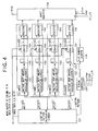
- FIG. 4 is a view showing a constituent example of the corrected image data calculation circuit 202 of the image display apparatus according to the present embodiment.
- all of the modulation signal wirings are turned ON (all of 4, 8, 16, and 12 are larger than 0), namely, a lighting pattern (1, 1, 1, 1).
- the lighting pattern corresponds to the lighting states of modulation signal wirings 0 to 3 in sequence from left.
- the voltage drop amount calculation circuit 102 calculates the luminance for the inputted lighting pattern.
- the voltage drop amount calculation circuit 102 calculates the volume of the luminance ⁇ L for the lighting pattern in consideration of the voltage drop amount defining the luminance ⁇ L when no voltage drop takes place as "1".
- the luminance ⁇ L is calculated on the basis of the above-described lighting pattern to be determined by the image data.
- the luminance ⁇ L is calculated on the basis of the lighting pattern that is updated by the following calculation.
- the accumulation circuit 103 accumulates the luminance in sequence corresponding to counting-up of the slot number counter and may calculate the luminance amount (the accumulated value) corresponding to each time slot in sequence.
- the comparator 104 compares the value of the image data (4, 8, 16, 12) for each modulation signal wiring with the accumulated luminance amount for each timing.
- FIG. 5A and FIG. 5B are typical views showing an example of comparing a value of the image data for each modulation signal wiring (corresponding to "a value of data to indicate the luminance of the pixel" of the present invention) with the accumulated value.
- a value of the image data for each modulation signal wiring corresponding to "a value of data to indicate the luminance of the pixel" of the present invention
- lateral axes of respective bar graphs corresponding to the inputted data D1[0] to D1[3] show a time.
- Each bar graph is formed in a shape such that rectangles corresponding to each period of time (time slot) shown in FIG. 5B are connected laterally.
- the size in a longitudinal axial direction (a vertical direction on the paper) of each rectangle indicates the luminance that is expected as the luminance of that period of time.
- the expected luminance is that assuming that no voltage drop takes place, and here, the expected luminance is defined as "1".
- the upper dotted portion in each rectangle indicates a loss of luminance due to loss of a signal.
- the dotted portion indicates a loss of luminance due to a voltage drop.
- the lower white portion in the rectangle indicates luminance ⁇ L to be calculated as the luminance that is obtained in practice in consideration of the voltage drop.
- a shaded portion corresponds to the luminance that is compensated by extending the length of the pulse by this correction calculation.
- image data D1 corresponding to modulation signal wirings 0 to 3 are 4, 8, 16, and 12.
- the value of the image data Data[0] to be inputted corresponding to a pixel connected to a modulation signal wiring 0 is "4".
- the pixel is driven for four time slots and at that point, driving has been terminated.
- the luminance for one time slot does not take a value "1" indicating the luminance to be required for the display device to be lowered (the dotted portion of the drawing).
- the accumulation circuit 103 accumulates the luminance amount when this luminance is lowered. In other words, calculating the sizes of the white portions in the rectangles for each period of time, they are accumulated. The sizes of the white portions are calculated by the voltage drop amount calculation circuit in accordance with the set lighting pattern. For the first period of time, the lighting pattern which is set on the basis of the image data is used.
- the lighting pattern calculation circuit 101 updates the lighting pattern from the next time slot.
- the lighting pattern is changed from (1, 1, 1, 1) into (0, 1, 1, 1). If the lighting pattern is updated, the voltage drop amount in the scan signal wiring is changed. Further, the influence of the voltage drop in the pulse width modulation is described in columns 0084 to 0095 of JP-A No. 2003-223131 (columns [0095] to [0107] of US 2003/0006976 A1 ).
- the voltage drop amount up to the time slot 7 and the voltage drop amount after the time slot 8 are different.
- the lighting pattern becomes (0, 1, 1, 1) the voltage drop amount is decreased.
- elevation of the electric potential on the scan signal wiring due to the voltage drop is decreased and the luminance ⁇ L of the display devices corresponding to the modulation signal wirings 1 to 3 are increased as compared to the previous period of time.
- FIG. 5A it is shown that the dotted portions are decreased and the luminance ⁇ L is increased.
- the luminance ⁇ L is calculated. By making calculation on the basis of the updated lighting state, it becomes possible to perform compensation with predicting the corrected lighting state.
- the lighting pattern calculation circuit 101 updates the lighting pattern from the next time slot.
- the lighting pattern is changed from (0, 1, 1, 1) into (0, 0, 1, 1). If the lighting pattern is updated, the voltage drop amount in the scan signal wiring is changed.
- the lighting pattern calculation circuit 101 updates the lighting pattern from the next time slot.
- the lighting pattern is changed from (0, 0, 1, 1) into (0, 0, 1, 0). If the lighting pattern is updated, the voltage drop amount in the scan signal wiring is changed.
- the lighting pattern calculation circuit 101 updates the lighting pattern from the next time slot. In FIG. 5A , the lighting pattern is changed from (0, 0, 1, 0) into (0, 0, 0, 0). Then, if the lighting pattern becomes (0, 0, 0, 0), calculation of the corrected data is terminated.
- the corrected image data D2 (7, 11, 22, 16) is decided for the inputted image data D1 (4, 8, 16, 12) in each modulation signal wiring.
- the corrected image data calculation circuit 202 outputs the decided corrected image data D2 to the modulation circuit 203.
- the modulation circuit 203 performs the pulse width modulation on the basis of the inputted corrected image data and outputs a drive signal to the display panel 205.
- the display panel 205 can display an image with reduced influence of the voltage drop in the scan signal wiring.
- the present embodiment can be applied to the display panel that is used in practice.
- change of the voltage drop can be also considered, so that the correction can be carried out at a high degree of accuracy.
- the display panel can display an excellent image having small influence of the voltage drop.
- a time width that is the same as an unit time for controlling the pulse width of the pulse width modulation signal is set as a time width for each period of time to calculate the luminance ⁇ L and the unit time to control the pulse width of the pulse width modulation signal is always fixed.
- the present embodiment is not limited to this.
- the time step may be changed.
- the time slot width of the position corresponding to a low tone may be made short and the time slot width of the position corresponding to a high tone may be made long. In this way, in the case that the time step is changed, accumulation in response to this time slot width may be carried out when accumulating the luminance.
- Counting-up of the slot number counter is defined to be changed in accordance with this.
- FIG. 9 is a flow chart for explaining the processing to make a time slot width uneven.
- the lighting pattern calculation circuit 101 analyzes the image data D1 and calculates the lighting pattern (S1 to S4).
- the accumulation circuit 103 carries out the accumulation calculation for each modulation signal wiring, however, according to the present embodiment, differently from FIG. 3 , the time slot width is multiplied to the luminance ⁇ T when performing accumulation to accumulate the luminance ⁇ T after accumulation.
- a lighting pattern ON[I] and a carry are generated so as to calculate correction data (S9 to S11).
- the time slot width ⁇ T is added.
- a visual feature of a human being has a tendency that, the lower a tone is for the volume of the luminance, the higher a resolution performance is, and the higher a tone is for the volume of the luminance, the lower a resolution performance is. In consideration of such a point, even from a point of view of an error of correction, when the time step is made uneven, a more excellent advantage can be obtained than the case of calculating the same step number evenly.
- the comparator 104 detects that the accumulated luminance is not less than the inputted image data, however, the present embodiment is not limited to this. For example, it may be detected that the accumulated luminance is larger than the image data, and it may be detected that the accumulated luminance is larger than the image data for a predetermined amount.
- the luminance accumulation circuits 100 are provided corresponding to all modulation signal wirings.
- the configuration such that the modulation signal wirings are divided into blocks each of which has a plurality of modulation signal wirings to calculate corrected image data will be described.
- the corrected image data of the input image data corresponding to the plurality of modulation signal wirings are calculated for each block.
- a configuration is employed below, in which a plurality of pixels to be connected to a common wiring are divided into plural pixel groups, each pixel group including plural pixels.
- the correction data to be used for obtaining the corrected image data corresponding to the pixels in the pixel group are calculated for each pixel group.
- the configuration such that a representative value showing lighting states of plural pixels belonging to a pixel group is used as data for evaluating a signal loss or data for evaluating luminance for each period of time after the signal loss occurs is employed below.
- FIG. 7 is a block diagram of the image display apparatus according to the present embodiment.
- the image display apparatus includes an inverse ⁇ conversion unit 701, a FIFO memory 702, a discrete corrected image data calculation circuit 703, a biaxial interpolation circuit 704, a modulation circuit 705, a display panel 706, a scan circuit 707, a high voltage electric source 708, and a timing generation circuit 709 for synchronizing each part.
- the image display apparatus is operated on the basis of a timing signal that is generated in the timing generation circuit 709 with reference to a horizontal synchronization HD and a vertical synchronization VD of image signal.
- the image data Data are inputted.
- the image data Data are represented as "Data" in FIG. 7 , however, the image data Data correspond to color image signals R, G, and B in color image display apparatus, respectively to be inputted in the inverse ⁇ conversion unit 701 in a point-sequence.
- the inverse ⁇ conversion unit 701 makes the input image data Data into inverse ⁇ conversion.
- the inverse ⁇ conversion unit 701 outputs the inverse ⁇ converted image data to the discrete corrected image data calculation circuit 703.
- a plurality of reference positions are arranged on the scan signal wiring.
- One pixel group (one block) corresponds to one reference position.
- the corrected image data corresponding to the reference position is discretely calculated.
- Each reference position is equivalent to a position of a modulation signal wiring representing each block when dividing a plurality of modulation signal wirings into blocks.
- the discrete corrected image data calculation circuit 703 determines "a plurality of discrete image data reference values (equivalent to a plurality of reference values)" also in a direction of a size (value) of the image data to calculate a discrete corrected image data CD for the image data reference value.
- the discrete corrected image data calculation circuit 703 outputs the discrete corrected image data CD to the biaxial interpolation circuit 704.
- the biaxial interpolation circuit 704 interpolates the corrected image data calculated for the discrete reference position and the discrete image data reference value in two axes, namely, in a horizontal direction of a screen and a direction of a size of data.
- any interpolation method can be employed.
- an example of the interpolation method is described in FIG. 22 of JP-A No. 2003-223131 , columns 0210 to 0218 and columns 0290 to 0294 (FIG. 22 of US 2003/0006976 A1 , columns [0241] to [0250] and [0332] to [0336]).
- the biaxial interpolation circuit calculates corrected image data corresponding to each pixel by carrying out interpolation calculation to be described later with reference to the image data to be transmitted from the FIFO memory 702 and the horizontal display position.
- the FIFO memory 702 is provided so as to absorb a calculation time in the discrete corrected image data calculation circuit 703.
- the image data delayed by the FIFO memory 702 and the corrected image data calculated by the discrete corrected image data calculation circuit 703 are synchronized to be inputted in the biaxial interpolation circuit.
- Read/Write or the like of the FIFO memory 702 is controlled by a timing signal (not illustrated) from the timing generation circuit 709.
- the corrected image data CD that is calculated in this way is inputted in a modulation circuit and a modulation signal is provided to each modulation signal wiring in accordance with the corrected image data.
- FIG. 6 is a view showing the structure of the discrete corrected image data calculation circuit 703 of the image display apparatus according to the present embodiment.
- the discrete corrected image data calculation circuit 703 includes a block lighting pattern calculation circuit 601, a voltage drop amount calculation circuit 602, an accumulation circuit 603, a comparator 604, a register for a comparison value 605, a pointer 606, a timing controller 607 for synchronizing each part, and a slot number counter 608 for counting the slot number.
- a block luminance accumulation circuit 600 is formed by the voltage drop amount calculation circuit 602, the accumulation circuit 603, the comparator 604, the register for a comparison value 605, and the pointer 606.
- a block in this case is defined to be a group as a bundle of a plurality of modulation signal wirings.
- a plurality of modulation signal wirings is divided into four blocks.
- the top block luminance accumulation circuit 600 (BLOCK1) is equivalent to a first correction unit.
- the second top block luminance accumulation circuit (BLOCK2) is equivalent to a second correction unit.
- FIG. 8 is a flow chart showing the operation of the discrete corrected image data calculation circuit 703 of the image display apparatus according to the present embodiment.
- the flow chart of FIG. 8 is partially indicated in a sequence processing for convenience of description.
- the block lighting pattern calculation circuit 601 sets, for each block, one value reflecting the lighting state of the pixels in the block.
- a lighting pattern is represented making the lighting state of each pixel into one bit of ON and OFF.
- the lighting pattern is represented by the data of the number of pixels x the information indicating the lighting state for each pixel (the number of pixels x 1 bit).
- the lighting pattern is represented by the data of the block number x the information indicating the lighting state for a plurality of pixels in each block.
- the lighting state of each block is represented by a value of three bits in proportion to a lighting ratio of a pixel in a block (a ratio of an ON element in a display device included in the block).
- the lighting pattern is represented by the data of the block number ⁇ 3 bits.
- the block lighting pattern calculation circuit 601 creates lighting patterns of respective blocks from the first block 0 up to a block NB - 1 on the basis of the image data DD1.
- the number of the image data not less than the data reference value DTH[J] is calculated for NB pieces of blocks from the block 0 up to the block NB - 1 (S21 to S26).
- step S22 the accumulated luminance value (L[I]) in each block is set at "0" and a value of the corrected image data (CData [I]) for the Jth image data reference value DTH [J] of the block I is set at "0".
- K pieces of the image data reference values DTH K is an integer not less than 1.
- the number of the image data not less than the image data reference value DTH[J], namely, from the first image data reference value DTH[0] up to the image data reference value DTH[K - 1] is calculated.
- the block lighting pattern calculation circuit 601 calculates a histogram of the image data for each block (S24).
- the block lighting pattern calculation circuit 601 counts a ratio that the modulation signal not less than a reference value of each image data is included for each block and converts it into a value of three bits (0 to 7 in a binary digit).
- the block lighting pattern calculation circuit 601 outputs a value of a lighting pattern represented by total 12 bits of 4 ⁇ 3 bits to the voltage drop amount calculation circuit 602.
- FIG. 12 shows an example of a histogram that is calculated for the image data during a certain one horizontal scanning period.
- the value indicating the lighting state of the pixels in the block is not limited to the lighting ratio of the pixels included in the block but various values such as the number of the lighting pixels, the number of the no-lighting pixels, and the accumulated value of the image data corresponding to the pixels included in the block can be employed.
- the voltage drop amount calculation circuit 602 calculates luminance ⁇ L of each block in accordance with the inputted lighting pattern of 12 bits.
- the voltage drop amount calculation circuit 602 calculates the luminance ⁇ L as a value of the luminance ⁇ L (a value showing the luminance of the pixel group) on the reference position on the center of the block when the pixels are not blocked (S29).
- the reference position is located on the center of each block.
- the value to be calculated from the reference position corresponds to the same spacious position as that in the case that the pixels are not blocked.
- the luminance ⁇ L based on the lighting pattern decided as described above on the basis of the inputted image data.
- the updated lighting pattern is calculated on and after the second period of time if the lighting pattern is updated on the basis of the accumulation results of the former luminance ⁇ L.
- the voltage drop amount calculation circuit 602 As the voltage drop amount calculation circuit 602, a memory having a parameter set in advance is used. Then, if the lighting pattern is inputted, the voltage drop amount calculation circuit 602 outputs the luminance ⁇ L[I] of that block to the accumulation circuit 603.
- the voltage drop amount calculation circuit 602 of the block 0 calculates the luminance of the block 0 on the basis of this lighting pattern. Then, the voltage drop amount calculation circuit 602 outputs the luminance of the block 0 to the accumulation circuit 603.
- the accumulation circuit 603 in synchronization with a timing signal from the timing controller 607 accumulates the luminance ⁇ L[I] in sequence in accordance with a counting-up of the slot number counter 608 and outputs the accumulated luminance L (corresponding to "an accumulated value obtained by an accumulation” of the present invention) in sequence (S30).
- the accumulation circuit 603 outputs the accumulated luminance L to the comparator 604.
- the accumulation circuit 603 accumulates the luminance ⁇ L of each period of time in sequence. However, since the luminance ⁇ L corresponding to a pixel becomes 0 after a period of time at which the accumulated value exceeds the image data for the pixel, the accumulation circuit 603 may be configured so as to stop the accumulation with respect to that pixel after that period of time.
- the comparator 604 may compare the accumulated luminance L[I] with the image data reference value DTH[POINT[I]] for each timing (S31). The comparator 604 makes Carry[I] into "High” when the accumulated luminance L[I] is not less than the image data reference value DTH[POINT[I] (Yes) (S31).
- the pointer 606 advances a pointer one and the value of the register for the comparison value 605 is changed one(S33).
- the image data reference value that is set for the image data is recorded in the register for the comparison value 605 and if the pointer is changed, the next image data reference value is inputted in the comparator.
- the value of the pointer is reset at a point of time when the accumulation is started and next, the smallest image data reference value is inputted in the comparator 604.
- an image data reference value "4" is set as an initial value. Then, when the accumulated luminance L[0] of the block 0 becomes larger than the image data reference value "4", Carry[0] is made into “High”. If Carry[0] is made into "High”, the pointer 606 advances the pointer one. Then, the register for the comparison value 605 sets the image data reference value at "8" (S33). In addition, if Carry[0] is made into "High”, the lighting patter is made into "6, 7, 7, 7". Further, by advancing the pointer one, a value val to be outputted by the comparison value register is updated, so that Carry[0] is made into "low”.
- a point of time when Carry of one block is made into High indicates that the corrected image data for the image data reference value that is a comparison target at that point of time is a count value of the slot number counter at that point of time.
- this corrected image data will be used as the corrected image data for its pixel.
- a Carry signal of each block is feed-backed to the block lighting pattern calculation circuit and in accordance with this, the block lighting pattern is updated in sequence.
- a lighting pattern of a block that its Carry is made into High moves into a lighting state for a next image data reference value.
- the corrected image data for the discrete image data reference value for each block can be calculated.
- the lighting state for each block is updated by a determination result by the comparator and in accordance with the updated lighting state, subsequent calculations are carried out.
- the reference value to be compared with the value obtained by the accumulation is defined as a discrete value such as 4, 8, 16, .... Then, the present embodiment is configured so as to obtain the corrected image data corresponding to each reference value.
- the configuration may be employed, in which all values (1, 2, 3, ... 255) that can be obtained by the image data are defined as a reference value, respectively. In this case, the interpolation in the direction of the size of the image data to be described later is not needed.
- the corrected image data that has been calculated in this way is inputted in the biaxial interpolation circuit 704, the interpolation is carried out in accordance with the image data and a horizontal position (a number of a modulation signal wiring) of a screen, and then, the corrected image data in accordance with each of them is calculated.
- FIG. 10 is a view for explaining the biaxial interpolation circuit 704 according to the present embodiment.
- the present embodiment is configured so as to obtain the corrected image data in accordance with a value (a reference value) within a value that can be obtained by the image data for each pixel group. Accordingly, the corrected image data corresponding to the image data of the value other than the reference value is obtained by interpolation.
- interpolation in accordance with the position of the pixel is also carried out.
- various interpolation processing can be employed, however, the following preferable configurations are shown.
- the biaxial interpolation circuit includes: a decoder 1001; read address generation circuits 1002, write address generation circuits 1003, and Dual Port memories 1004 which respectively corresponds to blocks; selectors 1005; and interpolation circuits 1, 2, and 3.
- a time slot value (CD) from the discrete corrected image data calculation circuit 703 and a Carry signal [I] for each block are provided in chronologic order.
- the write address generation circuit 1003 counts the number of carry signals from start of 1H. Counting-up an address for writing in sequence from 0 at timing when the signal becomes Carry, and using a time slot value CD in that case as the data for writing, the correction data of its block is written in the Dual Port memory 1004. Since Carry is made into High whenever the luminance of the block attains to an image data reference value, the correction value for the each image date reference value of the block will be stored in the Dual Port memory 1004.
- the image data DD2 and a horizontal display position X are inputted in the biaxial interpolation circuit 704.
- the read address generation circuit 1002 with reference to the size of the image data and the value of the horizontal display position X, an address for reading the data from the Dual Port memory 1004 is generated.
- the decoder 1001 is a circuit for switching the selectors 1005 with reference to the size of the image data and the value of the horizontal display position x.
- the selector 1005 further switches the value read from the Dual Port memory 1004 and provides this value to interpolation circuits 1 and 2 on a next stage.
- the interpolation circuits 1 and 2 are circuits to interpolate the corrected image data for each block in accordance with the horizontal display position x of the screen.
- the interpolation circuit 3 calculates the corrected image data DD3 by interpolating the results calculated by the interpolation circuits 1 and 2 in a direction of the size of the image data.
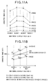
- FIG. 11 is a view for explaining a process when carrying out an interpolation calculation of the biaxial interpolation circuit 704.
- the correction value stored in the Dual Port memory 1004 corresponds to portions represented by marks such as a white circle, a white triangle, a black triangle, a black rhombus, and a black rectangle in FIG. 11A . No data between the correction values is stored.
- CA a correction value for a block n and an image data reference value DTH[k]
- CB the correction value for a block n + 1 and the image data reference value DTH[k]
- CC the correction value for the block n and the image data reference value DTH[k + 1]
- CD the correction value for a block n + 1 and the image data reference value DTH[k + 1]
- n is a number of block, satisfying Xn ⁇ x ⁇ Xn + 1 (Xn represents a horizontal display position corresponding to the nth block)
- k is a number of an image data reference value, satisfying DTH k ⁇ DD ⁇ 2 ⁇ DTH ⁇ k + 1 (DTH[k] represents the kth image data reference value).
- the interpolation calculation is carried out for the selected correction values CA, CB, CC, and CD corresponding to the size of the real image data and the horizontal display position by the interpolation circuits 1 to 3.
- C1 is calculated from CA and CB by the interpolation circuit 1 as the interpolation for the horizontal display position.
- C2 is calculated from CC and CD.
- corrected image data DD3 is calculated from c1 and c2 by the interpolation circuit 3 ( FIG. 11B shows a calculation formula in the case of a linear approximation).
- discretization is simultaneously carried out for the horizontal direction of the screen and the size of the image data, however, the present embodiment is not limited to this and for example, discretization may be carried out only in the direction of the size of the image data or only in the horizontal direction of the screen.
- the luminance is accumulated in a time direction, however, its time slot width is not necessarily even.
- the time slot width may be changed. For example, a short time slot width may be set in a portion having a small time slot corresponding to a low tone and a long time slot width may be set in a portion having a large time slot corresponding to a high tone.
- a short time slot width may be set in a portion having a small time slot corresponding to a low tone
- a long time slot width may be set in a portion having a large time slot corresponding to a high tone.
- the time slot width is changed in this way, upon accumulation of luminance, it is necessary to carry out accumulation in accordance with this time slot width and it is necessary to change the time slot width in accordance with this upon counting-up of the slot number counter.
- the number of the corrected image data to be referred by the interpolation circuit is decreased and this leads to simplification of a circuit.
- a visual feature of a human being has a tendency that, the lower a tone is, the higher a resolution performance is and the higher a tone is, the lower a resolution performance is with respect to the volume of the luminance.
- a more excellent advantage can be obtained than the case of calculating the same step number evenly.
- the comparator detects that the accumulated luminance takes a value not less than the image data reference value, however, the present embodiment is not limited to this in a precise sense. In other words, the comparator may detect that the accumulated luminance is larger than the image data reference value or may detect that the accumulated luminance is larger than the image data by a predetermined amount (in this case, although an error is increased, there is an advantage to some extent as correction).
- a signal loss an example to compensate a loss due to a voltage drop on a common wiring is cited.
- a correction to compensate a signal loss on a modulation signal wiring may be carried out.
- the compensation in the present application is not limited to that to completely compensate the loss in just proportion and it is enough to prevent deterioration of an image quality due to the loss.
- the size of the image data is corrected for input in a direction to compensate the shortage.
- the size of the image data generally has one upper limit, in order to carry out the correction preferably, it is necessary to control the corrected image data so as to be in the range of the upper limit.
- JP-A No. 2005-031636 ( US 2004/0257311 A1 ) is the configuration so as to decrease a visual feature by the halation of the image display apparatus.
- JP-A No. 07-181911 discloses the configuration so as to correct a uniformity of the display apparatus.
- the inventor(s) of the present invention has confirmed that a more preferable display can be realized by combining the corrections of the present invention.
- a light emission property of a phosphor has non-linearity to driving, by providing a table to cancel the non-linearity before the correction of the voltage drop or providing a table to cancel the non-linearity after the correction of the voltage drop, it is possible to preferably display an image.
- an image display apparatus including: a first correction unit for outputting data to determine a lighting time of a first pixel on the basis of data to indicate luminance of the first pixel, wherein the first correction unit carries out first correction to compensate a loss of the luminance of the first pixel; and a second correction unit for outputting data to determine a lighting time of a second pixel on the basis of data to indicate luminance of the second pixel, wherein the second correction unit carries out second correction to compensate a loss of the luminance of the second pixel by predicting a lighting state of the first pixel that is corrected by the first correction.
Landscapes
- Engineering & Computer Science (AREA)
- Physics & Mathematics (AREA)
- Computer Hardware Design (AREA)
- General Physics & Mathematics (AREA)
- Theoretical Computer Science (AREA)
- Control Of Indicators Other Than Cathode Ray Tubes (AREA)
Applications Claiming Priority (2)
| Application Number | Priority Date | Filing Date | Title |
|---|---|---|---|
| JP2006335839 | 2006-12-13 | ||
| JP2007312167A JP2008170970A (ja) | 2006-12-13 | 2007-12-03 | 画像表示装置及び画像表示装置の駆動方法 |
Publications (1)
| Publication Number | Publication Date |
|---|---|
| EP1933294A2 true EP1933294A2 (de) | 2008-06-18 |
Family
ID=39155334
Family Applications (1)
| Application Number | Title | Priority Date | Filing Date |
|---|---|---|---|
| EP07122812A Withdrawn EP1933294A2 (de) | 2006-12-13 | 2007-12-11 | Bildanzeigevorrichtung und Antriebsverfahren für die Bildanzeigevorrichtung |
Country Status (2)
| Country | Link |
|---|---|
| US (1) | US8085282B2 (de) |
| EP (1) | EP1933294A2 (de) |
Families Citing this family (6)
| Publication number | Priority date | Publication date | Assignee | Title |
|---|---|---|---|---|
| JP5340083B2 (ja) * | 2009-08-28 | 2013-11-13 | キヤノン株式会社 | 画像表示装置及びその輝度制御方法 |
| JP2011154187A (ja) * | 2010-01-27 | 2011-08-11 | Canon Inc | 画像表示装置 |
| WO2011162040A1 (ja) * | 2010-06-23 | 2011-12-29 | シャープ株式会社 | 画像表示装置および画像表示方法 |
| KR20160059573A (ko) * | 2014-11-18 | 2016-05-27 | 삼성디스플레이 주식회사 | 표시 장치 및 그 구동 방법 |
| WO2018235372A1 (ja) * | 2017-06-21 | 2018-12-27 | シャープ株式会社 | 画像表示装置 |
| KR102676645B1 (ko) * | 2019-10-10 | 2024-06-21 | 삼성디스플레이 주식회사 | 표시 장치 |
Citations (9)
| Publication number | Priority date | Publication date | Assignee | Title |
|---|---|---|---|---|
| JPH02257553A (ja) | 1989-03-30 | 1990-10-18 | Canon Inc | 画像形成装置の駆動方法 |
| JPH07181911A (ja) | 1993-12-22 | 1995-07-21 | Canon Inc | マルチ電子ビーム源とその駆動方法及びそれを用いた画像形成装置 |
| JPH08248920A (ja) | 1994-06-08 | 1996-09-27 | Canon Inc | 電子線発生方法とその装置、並びにその駆動方法、並びにそれを応用した画像形成方法とその装置 |
| US5659328A (en) | 1993-12-22 | 1997-08-19 | Canon Kabushiki Kaisha | Electron beam generating apparatus, image display apparatus, and method of driving the apparatus |
| US20030006976A1 (en) | 2001-06-14 | 2003-01-09 | Osamu Sagano | Image display apparatus |
| US20030030654A1 (en) | 2001-07-09 | 2003-02-13 | Canon Kabushiki Kaisha | Image display apparatus |
| JP2003223131A (ja) | 2001-06-14 | 2003-08-08 | Canon Inc | 画像表示装置 |
| JP2003233344A (ja) | 2001-07-09 | 2003-08-22 | Canon Inc | 画像表示装置 |
| US20040257311A1 (en) | 2003-06-20 | 2004-12-23 | Canon Kabushiki Kaisha | Image display apparatus |
Family Cites Families (14)
| Publication number | Priority date | Publication date | Assignee | Title |
|---|---|---|---|---|
| US6140985A (en) | 1995-06-05 | 2000-10-31 | Canon Kabushiki Kaisha | Image display apparatus |
| JP3049061B1 (ja) | 1999-02-26 | 2000-06-05 | キヤノン株式会社 | 画像表示装置及び画像表示方法 |
| JP3305283B2 (ja) | 1998-05-01 | 2002-07-22 | キヤノン株式会社 | 画像表示装置及び前記装置の制御方法 |
| JP2000056730A (ja) | 1998-06-05 | 2000-02-25 | Canon Inc | 画像形成装置及び画像形成方法 |
| JP2000310969A (ja) | 1999-02-25 | 2000-11-07 | Canon Inc | 画像表示装置及び画像表示装置の駆動方法 |
| JP3840027B2 (ja) | 1999-02-26 | 2006-11-01 | キヤノン株式会社 | 画像表示装置及び表示制御方法 |
| JP2000352952A (ja) | 1999-04-05 | 2000-12-19 | Canon Inc | 画像形成装置 |
| US7154457B2 (en) | 2001-06-14 | 2006-12-26 | Canon Kabushiki Kaisha | Image display apparatus |
| CN1265338C (zh) | 2001-11-21 | 2006-07-19 | 佳能株式会社 | 显示装置、其图像信号处理装置及驱动控制装置 |
| JP3789108B2 (ja) | 2002-10-09 | 2006-06-21 | キヤノン株式会社 | 画像表示装置 |
| JP4040454B2 (ja) | 2002-12-27 | 2008-01-30 | キヤノン株式会社 | 画像表示装置 |
| JP3789113B2 (ja) | 2003-01-17 | 2006-06-21 | キヤノン株式会社 | 画像表示装置 |
| JP4012118B2 (ja) | 2003-05-19 | 2007-11-21 | キヤノン株式会社 | 画像表示装置 |
| US20060208671A1 (en) * | 2005-03-15 | 2006-09-21 | Hitachi Displays, Ltd. | Display device |
-
2007
- 2007-12-06 US US11/951,776 patent/US8085282B2/en not_active Expired - Fee Related
- 2007-12-11 EP EP07122812A patent/EP1933294A2/de not_active Withdrawn
Patent Citations (12)
| Publication number | Priority date | Publication date | Assignee | Title |
|---|---|---|---|---|
| JPH02257553A (ja) | 1989-03-30 | 1990-10-18 | Canon Inc | 画像形成装置の駆動方法 |
| JPH07181911A (ja) | 1993-12-22 | 1995-07-21 | Canon Inc | マルチ電子ビーム源とその駆動方法及びそれを用いた画像形成装置 |
| US5659328A (en) | 1993-12-22 | 1997-08-19 | Canon Kabushiki Kaisha | Electron beam generating apparatus, image display apparatus, and method of driving the apparatus |
| JPH08248920A (ja) | 1994-06-08 | 1996-09-27 | Canon Inc | 電子線発生方法とその装置、並びにその駆動方法、並びにそれを応用した画像形成方法とその装置 |
| US5734361A (en) | 1994-06-08 | 1998-03-31 | Canon Kabushiki Kaisha | Electron-beam generating device having plurality of cold cathode elements, method of driving said device and image forming apparatus applying same |
| US20030006976A1 (en) | 2001-06-14 | 2003-01-09 | Osamu Sagano | Image display apparatus |
| JP2003223131A (ja) | 2001-06-14 | 2003-08-08 | Canon Inc | 画像表示装置 |
| US7079161B2 (en) | 2001-06-14 | 2006-07-18 | Canon Kabushiki Kaisha | Image display apparatus |
| US20030030654A1 (en) | 2001-07-09 | 2003-02-13 | Canon Kabushiki Kaisha | Image display apparatus |
| JP2003233344A (ja) | 2001-07-09 | 2003-08-22 | Canon Inc | 画像表示装置 |
| US20040257311A1 (en) | 2003-06-20 | 2004-12-23 | Canon Kabushiki Kaisha | Image display apparatus |
| JP2005031636A (ja) | 2003-06-20 | 2005-02-03 | Canon Inc | 画像表示装置 |
Also Published As
| Publication number | Publication date |
|---|---|
| US20080150969A1 (en) | 2008-06-26 |
| US8085282B2 (en) | 2011-12-27 |
Similar Documents
| Publication | Publication Date | Title |
|---|---|---|
| US8816945B2 (en) | Display apparatus | |
| JP6665228B2 (ja) | 表示装置の駆動方法 | |
| TWI395184B (zh) | 液晶顯示面板之背光亮度控制 | |
| JP4115330B2 (ja) | 画像形成装置の製造方法 | |
| US8085282B2 (en) | Image display apparatus and driving method of image display apparatus | |
| US20130169663A1 (en) | Apparatus and method for displaying images and apparatus and method for processing images | |
| CN114141210A (zh) | 显示装置以及显示控制器 | |
| CN101572058A (zh) | 背光驱动电路及其驱动方法 | |
| US20090015536A1 (en) | Liquid crystal display apparatus | |
| JP6438161B2 (ja) | 表示装置及び表示コントローラ | |
| US11145260B2 (en) | Display backlighting systems and methods for adaptive pulse width modulation and modulo pulse width modulation | |
| US8330748B2 (en) | Image display apparatus, correction circuit thereof and method for driving image display apparatus | |
| CN110599945B (zh) | Led显示装置及其驱动方法 | |
| US20060007202A1 (en) | Image display apparatus | |
| CN101202006B (zh) | 图像显示设备和图像显示设备的驱动方法 | |
| US20200168172A1 (en) | Display apparatus and method of controlling display apparatus | |
| JP2012088550A (ja) | 画像表示装置及びその制御方法 | |
| US8054305B2 (en) | Image display apparatus, correction circuit thereof and method for driving image display apparatus | |
| JP2007508578A (ja) | スクロールアドレス指定によるエレクトロルミネッセント表示装置 | |
| KR20210096729A (ko) | 표시 장치 및 그 구동 방법 | |
| US20060214883A1 (en) | Plasma display panel driving apparatus, signal processing method for plasma display panel and image display apparatus for plasma display panel | |
| JP2004045674A (ja) | 表示装置 | |
| JP2010079023A (ja) | 画像表示装置および方法 | |
| KR102319311B1 (ko) | 표시 장치 및 표시 장치의 구동 방법 | |
| KR100634951B1 (ko) | 표시 장치 |
Legal Events
| Date | Code | Title | Description |
|---|---|---|---|
| PUAI | Public reference made under article 153(3) epc to a published international application that has entered the european phase |
Free format text: ORIGINAL CODE: 0009012 |
|
| AK | Designated contracting states |
Kind code of ref document: A2 Designated state(s): AT BE BG CH CY CZ DE DK EE ES FI FR GB GR HU IE IS IT LI LT LU LV MC MT NL PL PT RO SE SI SK TR |
|
| AX | Request for extension of the european patent |
Extension state: AL BA HR MK RS |
|
| STAA | Information on the status of an ep patent application or granted ep patent |
Free format text: STATUS: THE APPLICATION HAS BEEN WITHDRAWN |
|
| 18W | Application withdrawn |
Effective date: 20110614 |