EP1931029A2 - Sägezahnoszillator mit gesteuerten Endpunkten und Verfahren dafür - Google Patents
Sägezahnoszillator mit gesteuerten Endpunkten und Verfahren dafür Download PDFInfo
- Publication number
- EP1931029A2 EP1931029A2 EP07121448A EP07121448A EP1931029A2 EP 1931029 A2 EP1931029 A2 EP 1931029A2 EP 07121448 A EP07121448 A EP 07121448A EP 07121448 A EP07121448 A EP 07121448A EP 1931029 A2 EP1931029 A2 EP 1931029A2
- Authority
- EP
- European Patent Office
- Prior art keywords
- circuit
- recited
- charge
- charge storage
- capacitor
- Prior art date
- Legal status (The legal status is an assumption and is not a legal conclusion. Google has not performed a legal analysis and makes no representation as to the accuracy of the status listed.)
- Granted
Links
Images




Classifications
-
- H—ELECTRICITY
- H03—ELECTRONIC CIRCUITRY
- H03K—PULSE TECHNIQUE
- H03K4/00—Generating pulses having essentially a finite slope or stepped portions
- H03K4/06—Generating pulses having essentially a finite slope or stepped portions having triangular shape
- H03K4/08—Generating pulses having essentially a finite slope or stepped portions having triangular shape having sawtooth shape
- H03K4/48—Generating pulses having essentially a finite slope or stepped portions having triangular shape having sawtooth shape using as active elements semiconductor devices
- H03K4/50—Generating pulses having essentially a finite slope or stepped portions having triangular shape having sawtooth shape using as active elements semiconductor devices in which a sawtooth voltage is produced across a capacitor
- H03K4/501—Generating pulses having essentially a finite slope or stepped portions having triangular shape having sawtooth shape using as active elements semiconductor devices in which a sawtooth voltage is produced across a capacitor the starting point of the flyback period being determined by the amplitude of the voltage across the capacitor, e.g. by a comparator
Definitions
- the subject matter herein relates generally to oscillators, and more particularly to oscillators such as sawtooth generators configured to produce accurate, high speed sawtooth signals having controlled endpoints.
- Oscillator circuits that have rapid charge / discharge characteristics are a vital part of many system architectures.
- a sawtooth waveform oscillator is used as a reference signal in the control loops of typical PWM-based power conversion systems, for example.
- Voltage mode switching DC/DC converter architectures often use this type of waveform to compare against an output voltage error signal, the result of which ultimately determines switch duty-cycle.
- Most current mode architectures require a sawtooth waveform to use as the basis for generation of a slope compensation signal.
- a controlled endpoint sawtooth signal generator circuit in accord with the teachings herein, comprises first and second charge sharing charge storage devices, and a source of charging current.
- the generator circuit is configured to operate in a first circuit state in which the first charge storage device is charged by the source of charging current and in which the first and second charge storage devices are mutually isolated, and, in a second circuit state in which the first and second charge storage devices are interconnected for charge sharing.
- One embodiment comprises a first charge storage device having an output node to which a charging source is coupled, and a second charge storage device coupled to the first charge storage device through a first controlled switch and to a first source of reference voltage through a second controlled switch.
- the first and second controlled switches are responsive to a control signal for mutually exclusive operation thereof.
- the control signal may be an externally provided trigger signal.
- the control signal may be produced internally by a circuit such as a comparator having a first input coupled to the first charge storage device, and a second input coupled to a second reference voltage source, and an output, wherein the output of the comparator is coupled to inputs of the first and second controlled switches.
- a method for generating an oscillating signal in accord with another aspect of the teachings herein, is carried out by applying charge to a first capacitor, sharing charge accumulated in the first capacitor with a second capacitor in response to a signal, and successively repeating the preceding steps.
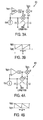
- Fig. 1A is a simplified circuit diagram showing a conventional ground referenced sawtooth waveform generator; Fig. 1B shows a waveform generated thereby.
- Fig. 2A is a simplified circuit diagram showing a conventional suspended endpoint sawtooth waveform generator; Fig. 2B shows a waveform generated thereby.
- Fig. 3A shows a first embodiment, in which a novel controlled endpoint sawtooth waveform generator is triggered by an internally produced pulse to produce a fast discharge charge sharing oscillator per the teachings herein;
- Fig. 3B shows the sawtooth waveform generated thereby.
- Figs. 4A and 4B describe a slow discharge charge sharing oscillator and sawtooth waveform using a modification of the foregoing architecture.
- Fig. 5 is a more detailed circuit diagram of Fig. 3A .
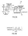
- Fig. 6A is a circuit diagram of a second embodiment in which the generator is fast discharging, triggered by an external signal;
- Fig. 6B shows a sawtooth waveform generated thereby.
- Figs. 7A , 7B are a more detailed circuit diagram of Fig 6A .
- a sawtooth waveform signal generator in which one or both of the endpoints of the sawtooth are suspended between the power supply rail and ground.
- a single source of reference voltage defines one end point of the sawtooth, and a novel switched capacitor pair charge sharing architecture establishes the other end point, the level of which may be related to capacitor ratio.
- the generator may be synchronized to oscillate by an internally or externally produced trigger.
- one embodiment of oscillator 300 comprises a first charge storage device in the form of a timing capacitor C1 and a second charge storage device in the form of a switched capacitor C2, interconnected by a low resistance controlled switch S1.
- a source of charging current I CHG is connected to the storage node of timing capacitor C1 and to the negative input of a comparator COMP.
- a source of reference voltage V REF3 is connected to the storage node of switched capacitor C2 through a resistive controlled switch S2 (the resistance of the switch is designated by R). Switches S1 and S1 are controlled to be mutually complementary.
- a source of reference voltage V REF1 is applied to the positive input of comparator COMP, the output of which is applied to the complementary control inputs of switches S1 and S2.
- a time delay element t d2 in the signal flow path between the comparator COMP and controlled switches S1, S2 may be inherent to the comparator, or may be an external component.
- capacitor C1 charges by current flow from I CHG , voltage on the capacitor rises slowly, forming the upslope portion of the sawtooth waveform shown in Fig. 3b .
- the output of comparator COMP becomes low, causing the states of switches S1 and S2 to reverse.
- Switch S1 is now closed and switch S2 open, to establish the ramp down portion of the sawtooth.
- capacitors C1, C1 are connected in parallel, rapidly sharing charge. Since the timing capacitor C1 initially is charged to a voltage greater than that of switched capacitor C2, capacitor C1 discharges into C2, as shown by the arrow in Fig. 3a , until the voltages on both capacitors are equalized at V REF2 .
- V REF2 is a floating voltage of a magnitude which is a function of the two capacitor voltages prior to discharge and the ratio of the two capacitances. Switches S1, S2 remain in the discharge position for the duration of the propagation delay t d2 , after which another charge accumulation cycle begins.
- V REF ⁇ 2 Q C ⁇ 1 + Q C ⁇ 2 / C ⁇ 1 + C ⁇ 2 , or
- V REF ⁇ 2 C ⁇ 1 * V REF ⁇ 1 + ( C ⁇ 2 * V REF ⁇ 3 ) / C ⁇ 1 + C ⁇ 2 .
- the circuit of Fig. 3a produces a slow charge sawtooth waveform, in which endpoints of the sawtooth are at V REF1 and V REF2 , and in which only one endpoint at V REF1 is established by a reference voltage source, the other endpoint being established internally by charge sharing between capacitors C1, C2.
- Fig. 4A shows a complementary implementation in which a fast charge, charge-sharing oscillator 400 is produced.
- This implementation is identical to that of Fig. 3a , except that the polarity of I CHG and the polarity of comparator COMP are reversed compared to the Fig. 3a implementation.
- Switches S1 and S2 initially are off and on, respectively.
- Switched capacitor C2 is charged through S2 to the switched capacitor reference V REF3.
- Timing capacitor C1 is discharged as current is sourced into Ichg, and the voltage across C1 drops toward V REF1.
- Capacitor C2 is charged to V REF3 during this interval through S2.
- Fig. 5 is a circuit diagram of an oscillator that implements the foregoing. This circuit generates a slow-charge, fast-discharge sawtooth output, as well as a synchronized pulsed output that corresponds to the fast-discharge interval.
- V REF1 1.25V
- V REF3 switched capacitor reference
- V REF ⁇ 2 C ⁇ 1 * V REF ⁇ 1 / C ⁇ 1 + C ⁇ 2 .
- V REF ⁇ 2 1 / 3 * V REF ⁇ 1 .
- V REF1 is imposed across R TRIM1 through transistors U9 and U11 to generate a reference current through transistor U11. This current is mirrored by multiple collector transistors U1 and U7.
- Transistor U1 provides general circuit bias, and transistor U7 provides the timing capacitor charge current I CHG .
- Transistor U9 provides temperature compensation for I CHG , to cause oscillator output frequency to be temperature invariant.
- the oscillator control comparator COMP in Fig. 5 comprises transistors U2-U5, and U13. This comparator trips when the voltage on timing capacitor C1 exceeds V REF1, or 1.25V, initiating the charge-sharing interval.
- the capacitor control switches are driven by an inverter / buffer string, X1 - X3, connected to the output of the comparator.
- transistor U7 sources I CHG onto timing capacitor C1.
- the voltage across switched capacitor C2 is held at 0V, by the ground-referred small switch transistor M8.
- Transistor M8 is sized such that a full discharge of capacitor C2 is assured during the charge interval, while minimizing C2 discharge current.
- the voltage on C1 is reduced by approximately 2/3, as derived above, to 0.45V.
- transistor M8 shunts the charge on capacitor C2 to ground, and the voltage on capacitor C1 begins to climb again as it accumulates charge due to I CHG , initiating another oscillator cycle.
- oscillator 600 switches S1 and S2 are controlled by a source of synchronization pulses which may be produced from within the oscillator circuit or from an external source of timing pulses to which the sawtooth is to be synchronized.
- the synchronization pulses which may be produced by a frequency control oscillator 602 as depicted, have a repetition rate corresponding to the frequency of the sawtooth and a width corresponding to the charge-sharing interval.
- the pulses are applied to the complimentary control inputs of switches S1 and S2 which function in a manner similar to that of the previous embodiment ( Fig. 3A ), in which the oscillator is synchronized internally by comparator COMP.
- charge current servo 604 comprises an integrator formed by transconductance comparator 604a receiving the sawtooth output and fixed reference V REF1, and in response, outputting the sawtooth to an integrating capacitor C3 and to a controlled current source 604b.
- the servo 604 translates the baseline of the sawtooth to V REF1. The high and low endpoints of the sawtooth per Fig.
- establishing the magnitude of the sawtooth are related by capacitor charge sharing based on the ratio between the two capacitors C1, C2, as in the previous embodiment, but with baseline, or waveform average value, determined by the fixed reference V REF1 as shown in Fig. 6A .
- Figs. 7A , 7B are a diagram of an illustrated circuit for implementing the architecture of Fig. 6A .
- This circuit generates a controlled amplitude slow-charge, fast-discharge sawtooth output, the oscillation frequency of which is controlled by a digital pulse train at 'control pulse' node 702, which is generated by a frequency control section 704.
- the frequency control section 704 is composed of a free-run reference oscillator 706, a synchronization pulse input buffer 708, a sync detection circuit 710, control logic 712 and a one-shot 714, interconnected as shown.
- a D flip-flop 716 is used to implement the one-shot function, and yields (in this example) a 50ns pulse when a pulse of longer-duration is applied at its complementary clock inputs (CLK and /CLK).
- the D flip-flop one-shot requires a clock signal that has pulse widths of adequate duration such that they exceed the programmed one-shot time, or 50ns in the example. This requirement thus applies to both the output of the free-run reference oscillator 706 and any synchronization signal that is applied at SYNC node 711.
- the free-run oscillator 716 is one that outputs a logic-level digital pulse-train at ⁇ 1MHz and 50% duty-cycle.
- the synchronization pulse input buffer 708 converts any digital signal on the SYNC node 711 to a logic-level signal with the same frequency and duty-cycle. If there is no signal at the SYNC input, 'control pulse' node 702 follows the output of the free-run reference oscillator 706. If a synchronization pulse is imposed on the SYNC input, the sync detection circuit 710 reconfigures control logic 712 such that 'control pulse' node 702 follows the output of the synchronization pulse input buffer, or the 'sync out' node.
- This signal is then imposed onto the clock inputs of one-shot 714.
- the final output of one-shot 714, and thus of the frequency control section 704, is a series of 50ns pulses that coincide with the rising edge of the signal on 'control pulse' node 702. The complement of this pulse train appears on 'freq in' node 715.
- timing capacitor C1 While 'freq in' is logic high, the switched capacitor C2, comprised of capacitive elements U10 and U11, is discharged to ground through the small switch transistor M2.
- Timing capacitor C1 implemented by capacitive element U12, is charged by the current sourced by one of the collectors in the multi-collector PNP, U9. The voltage on the timing capacitor C1 (U12) climbs until a 50ns pulse is output from the frequency control section. When this pulse is generated, 'freq in' is pulled to logic low, which disables transistor M2, and the timing and switched capacitors charge-share through a low-impedance switch transistor M5. At the instant before the switch transistors initiate a charge-sharing event, timing capacitor C1 has achieved a maximum voltage of V1.
- the switched capacitor C2 (U10+U11) is twice the value of the timing capacitor, and is referenced to ground through M2, the voltage across timing capacitor C1 is immediately reduced to 1/3 of the value achieved at the end of charging interval.
- This lower voltage, V2 is related to V1 by the capacitor ratio such that:
- V ⁇ 2 V ⁇ 1 * U ⁇ 12 / U ⁇ 12 + U ⁇ 10 + U ⁇ 11
- V AVG V ⁇ 1 + V ⁇ 2 / 2 ,
- V ⁇ 2 1 / 3 * V ⁇ 1
- V AVG 2 / 3 * V ⁇ 1
- transistor M5 is disabled, and transistor M2 is enabled, re-initiating another charging interval.
- the resultant voltage across the timing capacitor U12 thus becomes slow-charge, fast discharge sawtooth, output at 'osc out' node 716.
- the 'osc out' sawtooth oscillation rate directly follows the frequency control section. This output is also accompanied with a pulse train output at the 'pulse out' node, each pulse representing a 50ns discharge interval.
- the sawtooth waveform produced at 'osc out' node 716 is imposed onto an integration amplifier 718, comprised of transistors U1-U5, which forms an error signal related to the difference in the average-value of the sawtooth waveform and a reference voltage.
- This reference which corresponds to V REF1 in Fig. 6B , is formed by dividing the 2.7V supply rail voltage using resistors R5 and R14 to 0.9V, and is input to the noninverting input of the integrating amplifier 718 at 'ref avg' node 720.
- the output of amplifier 718, or collector of U5 drives a voltage-to-current converter 722, comprised of transistors U7 and U9.
- the multi-collector PNP transistor, U9 provides charging current to timing capacitor U12. These elements act to servo the timing capacitor U12 charging currents such that the average value of the sawtooth waveform is 0.9V. For example, if the average value of the sawtooth is lower than 0.9V, the output of the amplifier 718, or collector of U5, will rise. This, in turn, increases the voltage across R2 via the emitter-follower U7, and in turn the current in U7 will increase. This current is mirrored by U9, increasing the charging current onto the timing capacitor U12, increasing the charging rate. As the charge interval is fixed by the frequency control pulse, the voltage achieved during that charging interval (V1) will also increase.
- the embodiments described herein provide an oscillator circuit, particularly useful for generating a sawtooth signal having endpoints that are controlled to specific values, doing so by a novel capacitor charge sharing methodology in which a capacitor is charged for the upslope, and charge sharing with another capacitor for the downslope. Both endpoints thereby are controlled, using as few as one fixed voltage reference, having both endpoints related by capacitor ratios.
- high discharge currents are isolated with respect to the capacitors, and thus do not corrupt the supply rail or ground reference.
Landscapes
- Engineering & Computer Science (AREA)
- Power Engineering (AREA)
- Dc-Dc Converters (AREA)
- Pulse Circuits (AREA)
- Details Of Television Scanning (AREA)
Priority Applications (1)
| Application Number | Priority Date | Filing Date | Title |
|---|---|---|---|
| EP11009533.8A EP2426819B1 (de) | 2006-12-04 | 2007-11-23 | Sägezahnoszillator mit gesteuerten Endpunkten und Verfahren dafür |
Applications Claiming Priority (1)
| Application Number | Priority Date | Filing Date | Title |
|---|---|---|---|
| US11/607,899 US7583113B2 (en) | 2006-12-04 | 2006-12-04 | Sawtooth oscillator having controlled endpoints and methodology therefor |
Related Child Applications (2)
| Application Number | Title | Priority Date | Filing Date |
|---|---|---|---|
| EP11009533.8A Division EP2426819B1 (de) | 2006-12-04 | 2007-11-23 | Sägezahnoszillator mit gesteuerten Endpunkten und Verfahren dafür |
| EP11009533.8 Division-Into | 2011-12-01 |
Publications (3)
| Publication Number | Publication Date |
|---|---|
| EP1931029A2 true EP1931029A2 (de) | 2008-06-11 |
| EP1931029A3 EP1931029A3 (de) | 2010-03-10 |
| EP1931029B1 EP1931029B1 (de) | 2013-01-16 |
Family
ID=39156298
Family Applications (2)
| Application Number | Title | Priority Date | Filing Date |
|---|---|---|---|
| EP11009533.8A Not-in-force EP2426819B1 (de) | 2006-12-04 | 2007-11-23 | Sägezahnoszillator mit gesteuerten Endpunkten und Verfahren dafür |
| EP07121448A Not-in-force EP1931029B1 (de) | 2006-12-04 | 2007-11-23 | Sägezahnoszillator mit gesteuerten Endpunkten und Verfahren dafür |
Family Applications Before (1)
| Application Number | Title | Priority Date | Filing Date |
|---|---|---|---|
| EP11009533.8A Not-in-force EP2426819B1 (de) | 2006-12-04 | 2007-11-23 | Sägezahnoszillator mit gesteuerten Endpunkten und Verfahren dafür |
Country Status (4)
| Country | Link |
|---|---|
| US (1) | US7583113B2 (de) |
| EP (2) | EP2426819B1 (de) |
| CN (1) | CN101257292B (de) |
| TW (1) | TWI418149B (de) |
Cited By (1)
| Publication number | Priority date | Publication date | Assignee | Title |
|---|---|---|---|---|
| FR2975246A1 (fr) * | 2011-05-09 | 2012-11-16 | St Microelectronics Grenoble 2 | Dispositif de generation d'un signal en dents de scie |
Families Citing this family (10)
| Publication number | Priority date | Publication date | Assignee | Title |
|---|---|---|---|---|
| US20080143408A1 (en) * | 2006-12-19 | 2008-06-19 | Fabrice Paillet | Pulse width modulator |
| JP2008167091A (ja) * | 2006-12-28 | 2008-07-17 | Matsushita Electric Ind Co Ltd | 三角波発生回路およびpwm変調回路 |
| CN103051308B (zh) * | 2013-01-09 | 2015-04-29 | 武汉科技大学 | 一种基于忆阻器的方波和锯齿波产生电路 |
| US8803569B1 (en) | 2013-06-27 | 2014-08-12 | International Business Machines Corporation | Ramp generator using operational amplifier based integration and switched capacitor techniques |
| CN106026989B (zh) * | 2016-06-17 | 2019-03-29 | 沈阳工业大学 | 数字信号控制的连续时间函数信号生成电路 |
| US10924261B2 (en) * | 2017-05-22 | 2021-02-16 | Arm Limited | Efficient power distribution |
| US10997322B2 (en) | 2017-05-22 | 2021-05-04 | Arm Limited | Efficient power distribution |
| TWI668957B (zh) * | 2018-05-15 | 2019-08-11 | 華邦電子股份有限公司 | 震盪器電路 |
| US10778199B2 (en) * | 2018-11-20 | 2020-09-15 | Analog Devices International Unlimited Company | Oscillator temperature compensation techniques |
| US11394308B1 (en) | 2021-05-05 | 2022-07-19 | Arm Limited | Apparatuses and methods for power isolation |
Citations (2)
| Publication number | Priority date | Publication date | Assignee | Title |
|---|---|---|---|---|
| US6163190A (en) | 1998-06-22 | 2000-12-19 | Ricoh Company, Ltd. | Hysteresis comparator circuit consuming a small current |
| WO2006117236A2 (en) | 2005-05-05 | 2006-11-09 | Infineon Technologies Ag | Apparatus and method for reducing power comsumption within an oscillator |
Family Cites Families (10)
| Publication number | Priority date | Publication date | Assignee | Title |
|---|---|---|---|---|
| DE2511642C3 (de) * | 1975-03-17 | 1980-09-11 | Siemens Ag, 1000 Berlin Und 8000 Muenchen | Schaltungsanordnung zur Amplitudenregelung eines Sägezahngenerators |
| NL9201053A (nl) * | 1992-06-15 | 1994-01-03 | Koninkl Philips Electronics Nv | Switched capacitor ladingspomp, alsmede zaagtandoscillator voorzien van een dergelijke switched capacitor ladingspomp. |
| US5502410A (en) * | 1994-03-14 | 1996-03-26 | Motorola, Inc. | Circuit for providing a voltage ramp signal |
| KR0134914B1 (ko) * | 1995-06-29 | 1998-04-25 | 김광호 | 아날로그 방식의 발진회로 |
| US5969513A (en) * | 1998-03-24 | 1999-10-19 | Volterra Semiconductor Corporation | Switched capacitor current source for use in switching regulators |
| DE60039101D1 (de) * | 2000-03-31 | 2008-07-17 | St Microelectronics Srl | Integrierter Generator einer langsamen Spannungsrampe |
| GB2368474A (en) * | 2000-09-28 | 2002-05-01 | Seiko Epson Corp | Sawtooth or triangular waveform generator |
| US6930520B2 (en) * | 2003-05-13 | 2005-08-16 | Intersil Americas Inc. | High bandwidth feed-forward oscillator |
| US7355461B2 (en) * | 2004-12-15 | 2008-04-08 | Asahi Kasei Microsystems Co., Ltd. | Waveform generating circuit and spread spectrum clock generator |
| JP2007074190A (ja) * | 2005-09-06 | 2007-03-22 | Rohm Co Ltd | 三角波発生回路ならびにそれを用いたパルス幅変調器およびスイッチングレギュレータ |
-
2006
- 2006-12-04 US US11/607,899 patent/US7583113B2/en active Active
-
2007
- 2007-10-25 TW TW096140126A patent/TWI418149B/zh not_active IP Right Cessation
- 2007-11-16 CN CN2007101872322A patent/CN101257292B/zh not_active Expired - Fee Related
- 2007-11-23 EP EP11009533.8A patent/EP2426819B1/de not_active Not-in-force
- 2007-11-23 EP EP07121448A patent/EP1931029B1/de not_active Not-in-force
Patent Citations (2)
| Publication number | Priority date | Publication date | Assignee | Title |
|---|---|---|---|---|
| US6163190A (en) | 1998-06-22 | 2000-12-19 | Ricoh Company, Ltd. | Hysteresis comparator circuit consuming a small current |
| WO2006117236A2 (en) | 2005-05-05 | 2006-11-09 | Infineon Technologies Ag | Apparatus and method for reducing power comsumption within an oscillator |
Cited By (1)
| Publication number | Priority date | Publication date | Assignee | Title |
|---|---|---|---|---|
| FR2975246A1 (fr) * | 2011-05-09 | 2012-11-16 | St Microelectronics Grenoble 2 | Dispositif de generation d'un signal en dents de scie |
Also Published As
| Publication number | Publication date |
|---|---|
| US7583113B2 (en) | 2009-09-01 |
| EP2426819B1 (de) | 2014-03-19 |
| TW200830717A (en) | 2008-07-16 |
| EP1931029B1 (de) | 2013-01-16 |
| EP1931029A3 (de) | 2010-03-10 |
| EP2426819A1 (de) | 2012-03-07 |
| TWI418149B (zh) | 2013-12-01 |
| US20080129400A1 (en) | 2008-06-05 |
| CN101257292B (zh) | 2011-12-28 |
| CN101257292A (zh) | 2008-09-03 |
Similar Documents
| Publication | Publication Date | Title |
|---|---|---|
| EP1931029B1 (de) | Sägezahnoszillator mit gesteuerten Endpunkten und Verfahren dafür | |
| US7109804B2 (en) | Precision relaxation oscillator without comparator delay errors | |
| US8884676B2 (en) | Clock generator with duty cycle control and method | |
| TWI470932B (zh) | 差分式振幅控制鋸齒波產生器及產生雙差分式鋸齒波信號之方法 | |
| US8164357B2 (en) | Digital noise protection circuit and method | |
| CN103997317A (zh) | 一种显著提高控制电流—输出频率线性度的张弛振荡器 | |
| CN102820852B (zh) | 用于产生振荡信号的方法和振荡器电路 | |
| KR20070081099A (ko) | 발진회로 | |
| US11863191B2 (en) | Combining voltage ramps to create linear voltage ramp | |
| US4024414A (en) | Electrical circuit means for detecting the frequency of input signals | |
| US6924633B2 (en) | Pulse width modulation controller with double pulse immunity | |
| CN110708044B (zh) | 一种锯齿波产生电路及升降压变换器 | |
| US7663351B2 (en) | Synchronization circuitry for multiple power converters coupled at a common node | |
| CN112104203B (zh) | 开关限流电路及电源芯片 | |
| JP4520998B2 (ja) | 充電昇圧器を伴うパルス電流源回路 | |
| WO2018192790A1 (en) | Oscillator circuit with comparator delay cancelation | |
| US7391242B1 (en) | Sawtooth waveform generator | |
| CN117118207B (zh) | 一种用于大型mlcc的cot模式pwm驱动电路 | |
| JP6956052B2 (ja) | ゲート制御回路、電源回路及びインバータ回路 | |
| JP7629490B1 (ja) | 発振回路 | |
| KR940010481A (ko) | 저주파 발진기 | |
| JP2001157443A (ja) | パルス制御回路及び同期整流回路 | |
| US8294496B2 (en) | Sawtooth oscillator | |
| RU2254670C1 (ru) | Управляемый генератор импульсов | |
| SU1413700A1 (ru) | Генератор |
Legal Events
| Date | Code | Title | Description |
|---|---|---|---|
| PUAI | Public reference made under article 153(3) epc to a published international application that has entered the european phase |
Free format text: ORIGINAL CODE: 0009012 |
|
| AK | Designated contracting states |
Kind code of ref document: A2 Designated state(s): AT BE BG CH CY CZ DE DK EE ES FI FR GB GR HU IE IS IT LI LT LU LV MC MT NL PL PT RO SE SI SK TR |
|
| AX | Request for extension of the european patent |
Extension state: AL BA HR MK RS |
|
| 17P | Request for examination filed |
Effective date: 20081212 |
|
| PUAL | Search report despatched |
Free format text: ORIGINAL CODE: 0009013 |
|
| AK | Designated contracting states |
Kind code of ref document: A3 Designated state(s): AT BE BG CH CY CZ DE DK EE ES FI FR GB GR HU IE IS IT LI LT LU LV MC MT NL PL PT RO SE SI SK TR |
|
| AX | Request for extension of the european patent |
Extension state: AL BA HR MK RS |
|
| AKX | Designation fees paid |
Designated state(s): AT BE BG CH CY CZ DE DK EE ES FI FR GB GR HU IE IS IT LI LT LU LV MC MT NL PL PT RO SE SI SK TR |
|
| 17Q | First examination report despatched |
Effective date: 20110606 |
|
| RAP1 | Party data changed (applicant data changed or rights of an application transferred) |
Owner name: LINEAR TECHNOLOGY CORPORATION |
|
| GRAP | Despatch of communication of intention to grant a patent |
Free format text: ORIGINAL CODE: EPIDOSNIGR1 |
|
| GRAS | Grant fee paid |
Free format text: ORIGINAL CODE: EPIDOSNIGR3 |
|
| GRAP | Despatch of communication of intention to grant a patent |
Free format text: ORIGINAL CODE: EPIDOSNIGR1 |
|
| GRAC | Information related to communication of intention to grant a patent modified |
Free format text: ORIGINAL CODE: EPIDOSCIGR1 |
|
| GRAJ | Information related to disapproval of communication of intention to grant by the applicant or resumption of examination proceedings by the epo deleted |
Free format text: ORIGINAL CODE: EPIDOSDIGR1 |
|
| GRAS | Grant fee paid |
Free format text: ORIGINAL CODE: EPIDOSNIGR3 |
|
| GRAP | Despatch of communication of intention to grant a patent |
Free format text: ORIGINAL CODE: EPIDOSNIGR1 |
|
| GRAA | (expected) grant |
Free format text: ORIGINAL CODE: 0009210 |
|
| AK | Designated contracting states |
Kind code of ref document: B1 Designated state(s): AT BE BG CH CY CZ DE DK EE ES FI FR GB GR HU IE IS IT LI LT LU LV MC MT NL PL PT RO SE SI SK TR |
|
| REG | Reference to a national code |
Ref country code: GB Ref legal event code: FG4D |
|
| REG | Reference to a national code |
Ref country code: CH Ref legal event code: EP |
|
| REG | Reference to a national code |
Ref country code: IE Ref legal event code: FG4D |
|
| REG | Reference to a national code |
Ref country code: AT Ref legal event code: REF Ref document number: 594357 Country of ref document: AT Kind code of ref document: T Effective date: 20130215 Ref country code: CH Ref legal event code: EP |
|
| REG | Reference to a national code |
Ref country code: DE Ref legal event code: R096 Ref document number: 602007028056 Country of ref document: DE Effective date: 20130314 |
|
| REG | Reference to a national code |
Ref country code: NL Ref legal event code: T3 |
|
| REG | Reference to a national code |
Ref country code: AT Ref legal event code: MK05 Ref document number: 594357 Country of ref document: AT Kind code of ref document: T Effective date: 20130116 |
|
| REG | Reference to a national code |
Ref country code: LT Ref legal event code: MG4D |
|
| PG25 | Lapsed in a contracting state [announced via postgrant information from national office to epo] |
Ref country code: ES Free format text: LAPSE BECAUSE OF FAILURE TO SUBMIT A TRANSLATION OF THE DESCRIPTION OR TO PAY THE FEE WITHIN THE PRESCRIBED TIME-LIMIT Effective date: 20130427 Ref country code: BE Free format text: LAPSE BECAUSE OF FAILURE TO SUBMIT A TRANSLATION OF THE DESCRIPTION OR TO PAY THE FEE WITHIN THE PRESCRIBED TIME-LIMIT Effective date: 20130116 Ref country code: AT Free format text: LAPSE BECAUSE OF FAILURE TO SUBMIT A TRANSLATION OF THE DESCRIPTION OR TO PAY THE FEE WITHIN THE PRESCRIBED TIME-LIMIT Effective date: 20130116 Ref country code: BG Free format text: LAPSE BECAUSE OF FAILURE TO SUBMIT A TRANSLATION OF THE DESCRIPTION OR TO PAY THE FEE WITHIN THE PRESCRIBED TIME-LIMIT Effective date: 20130416 Ref country code: IS Free format text: LAPSE BECAUSE OF FAILURE TO SUBMIT A TRANSLATION OF THE DESCRIPTION OR TO PAY THE FEE WITHIN THE PRESCRIBED TIME-LIMIT Effective date: 20130516 Ref country code: LT Free format text: LAPSE BECAUSE OF FAILURE TO SUBMIT A TRANSLATION OF THE DESCRIPTION OR TO PAY THE FEE WITHIN THE PRESCRIBED TIME-LIMIT Effective date: 20130116 Ref country code: SE Free format text: LAPSE BECAUSE OF FAILURE TO SUBMIT A TRANSLATION OF THE DESCRIPTION OR TO PAY THE FEE WITHIN THE PRESCRIBED TIME-LIMIT Effective date: 20130116 |
|
| PG25 | Lapsed in a contracting state [announced via postgrant information from national office to epo] |
Ref country code: GR Free format text: LAPSE BECAUSE OF FAILURE TO SUBMIT A TRANSLATION OF THE DESCRIPTION OR TO PAY THE FEE WITHIN THE PRESCRIBED TIME-LIMIT Effective date: 20130417 Ref country code: PL Free format text: LAPSE BECAUSE OF FAILURE TO SUBMIT A TRANSLATION OF THE DESCRIPTION OR TO PAY THE FEE WITHIN THE PRESCRIBED TIME-LIMIT Effective date: 20130116 Ref country code: FI Free format text: LAPSE BECAUSE OF FAILURE TO SUBMIT A TRANSLATION OF THE DESCRIPTION OR TO PAY THE FEE WITHIN THE PRESCRIBED TIME-LIMIT Effective date: 20130116 Ref country code: PT Free format text: LAPSE BECAUSE OF FAILURE TO SUBMIT A TRANSLATION OF THE DESCRIPTION OR TO PAY THE FEE WITHIN THE PRESCRIBED TIME-LIMIT Effective date: 20130516 Ref country code: LV Free format text: LAPSE BECAUSE OF FAILURE TO SUBMIT A TRANSLATION OF THE DESCRIPTION OR TO PAY THE FEE WITHIN THE PRESCRIBED TIME-LIMIT Effective date: 20130116 Ref country code: SI Free format text: LAPSE BECAUSE OF FAILURE TO SUBMIT A TRANSLATION OF THE DESCRIPTION OR TO PAY THE FEE WITHIN THE PRESCRIBED TIME-LIMIT Effective date: 20130116 |
|
| PG25 | Lapsed in a contracting state [announced via postgrant information from national office to epo] |
Ref country code: DK Free format text: LAPSE BECAUSE OF FAILURE TO SUBMIT A TRANSLATION OF THE DESCRIPTION OR TO PAY THE FEE WITHIN THE PRESCRIBED TIME-LIMIT Effective date: 20130116 Ref country code: SK Free format text: LAPSE BECAUSE OF FAILURE TO SUBMIT A TRANSLATION OF THE DESCRIPTION OR TO PAY THE FEE WITHIN THE PRESCRIBED TIME-LIMIT Effective date: 20130116 Ref country code: RO Free format text: LAPSE BECAUSE OF FAILURE TO SUBMIT A TRANSLATION OF THE DESCRIPTION OR TO PAY THE FEE WITHIN THE PRESCRIBED TIME-LIMIT Effective date: 20130116 Ref country code: EE Free format text: LAPSE BECAUSE OF FAILURE TO SUBMIT A TRANSLATION OF THE DESCRIPTION OR TO PAY THE FEE WITHIN THE PRESCRIBED TIME-LIMIT Effective date: 20130116 Ref country code: CZ Free format text: LAPSE BECAUSE OF FAILURE TO SUBMIT A TRANSLATION OF THE DESCRIPTION OR TO PAY THE FEE WITHIN THE PRESCRIBED TIME-LIMIT Effective date: 20130116 |
|
| PLBE | No opposition filed within time limit |
Free format text: ORIGINAL CODE: 0009261 |
|
| STAA | Information on the status of an ep patent application or granted ep patent |
Free format text: STATUS: NO OPPOSITION FILED WITHIN TIME LIMIT |
|
| PG25 | Lapsed in a contracting state [announced via postgrant information from national office to epo] |
Ref country code: CY Free format text: LAPSE BECAUSE OF FAILURE TO SUBMIT A TRANSLATION OF THE DESCRIPTION OR TO PAY THE FEE WITHIN THE PRESCRIBED TIME-LIMIT Effective date: 20130116 |
|
| 26N | No opposition filed |
Effective date: 20131017 |
|
| REG | Reference to a national code |
Ref country code: DE Ref legal event code: R097 Ref document number: 602007028056 Country of ref document: DE Effective date: 20131017 |
|
| REG | Reference to a national code |
Ref country code: CH Ref legal event code: PL |
|
| PG25 | Lapsed in a contracting state [announced via postgrant information from national office to epo] |
Ref country code: MC Free format text: LAPSE BECAUSE OF FAILURE TO SUBMIT A TRANSLATION OF THE DESCRIPTION OR TO PAY THE FEE WITHIN THE PRESCRIBED TIME-LIMIT Effective date: 20130116 Ref country code: LI Free format text: LAPSE BECAUSE OF NON-PAYMENT OF DUE FEES Effective date: 20131130 Ref country code: CH Free format text: LAPSE BECAUSE OF NON-PAYMENT OF DUE FEES Effective date: 20131130 |
|
| REG | Reference to a national code |
Ref country code: IE Ref legal event code: MM4A |
|
| PG25 | Lapsed in a contracting state [announced via postgrant information from national office to epo] |
Ref country code: IE Free format text: LAPSE BECAUSE OF NON-PAYMENT OF DUE FEES Effective date: 20131123 |
|
| PG25 | Lapsed in a contracting state [announced via postgrant information from national office to epo] |
Ref country code: TR Free format text: LAPSE BECAUSE OF FAILURE TO SUBMIT A TRANSLATION OF THE DESCRIPTION OR TO PAY THE FEE WITHIN THE PRESCRIBED TIME-LIMIT Effective date: 20130116 |
|
| PG25 | Lapsed in a contracting state [announced via postgrant information from national office to epo] |
Ref country code: LU Free format text: LAPSE BECAUSE OF NON-PAYMENT OF DUE FEES Effective date: 20131123 Ref country code: HU Free format text: LAPSE BECAUSE OF FAILURE TO SUBMIT A TRANSLATION OF THE DESCRIPTION OR TO PAY THE FEE WITHIN THE PRESCRIBED TIME-LIMIT; INVALID AB INITIO Effective date: 20071123 |
|
| PG25 | Lapsed in a contracting state [announced via postgrant information from national office to epo] |
Ref country code: MT Free format text: LAPSE BECAUSE OF FAILURE TO SUBMIT A TRANSLATION OF THE DESCRIPTION OR TO PAY THE FEE WITHIN THE PRESCRIBED TIME-LIMIT Effective date: 20130116 |
|
| REG | Reference to a national code |
Ref country code: FR Ref legal event code: PLFP Year of fee payment: 9 |
|
| REG | Reference to a national code |
Ref country code: FR Ref legal event code: PLFP Year of fee payment: 10 |
|
| REG | Reference to a national code |
Ref country code: FR Ref legal event code: PLFP Year of fee payment: 11 |
|
| REG | Reference to a national code |
Ref country code: FR Ref legal event code: PLFP Year of fee payment: 12 |
|
| REG | Reference to a national code |
Ref country code: DE Ref legal event code: R082 Ref document number: 602007028056 Country of ref document: DE Representative=s name: MUELLER-BORE & PARTNER PATENTANWAELTE PARTG MB, DE Ref country code: DE Ref legal event code: R081 Ref document number: 602007028056 Country of ref document: DE Owner name: ANALOG DEVICES INTERNATIONAL UNLIMITED COMPANY, IE Free format text: FORMER OWNER: LINEAR TECHNOLOGY CORPORATION, MILPITAS, CALIF., US Ref country code: DE Ref legal event code: R082 Ref document number: 602007028056 Country of ref document: DE Representative=s name: WITHERS & ROGERS LLP, DE |
|
| REG | Reference to a national code |
Ref country code: DE Ref legal event code: R082 Ref document number: 602007028056 Country of ref document: DE Representative=s name: WITHERS & ROGERS LLP, DE |
|
| REG | Reference to a national code |
Ref country code: GB Ref legal event code: 732E Free format text: REGISTERED BETWEEN 20210930 AND 20211006 |
|
| PGFP | Annual fee paid to national office [announced via postgrant information from national office to epo] |
Ref country code: NL Payment date: 20211020 Year of fee payment: 15 |
|
| REG | Reference to a national code |
Ref country code: NL Ref legal event code: PD Owner name: ANALOG DEVICES INTERNATIONAL UNLIMITED COMPANY; IE Free format text: DETAILS ASSIGNMENT: CHANGE OF OWNER(S), ASSIGNMENT; FORMER OWNER NAME: LINEAR TECHNOLOGY LLC Effective date: 20211216 |
|
| PGFP | Annual fee paid to national office [announced via postgrant information from national office to epo] |
Ref country code: DE Payment date: 20211020 Year of fee payment: 15 Ref country code: GB Payment date: 20211020 Year of fee payment: 15 |
|
| PGFP | Annual fee paid to national office [announced via postgrant information from national office to epo] |
Ref country code: IT Payment date: 20211025 Year of fee payment: 15 Ref country code: FR Payment date: 20211020 Year of fee payment: 15 |
|
| REG | Reference to a national code |
Ref country code: DE Ref legal event code: R119 Ref document number: 602007028056 Country of ref document: DE |
|
| REG | Reference to a national code |
Ref country code: NL Ref legal event code: MM Effective date: 20221201 |
|
| GBPC | Gb: european patent ceased through non-payment of renewal fee |
Effective date: 20221123 |
|
| PG25 | Lapsed in a contracting state [announced via postgrant information from national office to epo] |
Ref country code: NL Free format text: LAPSE BECAUSE OF NON-PAYMENT OF DUE FEES Effective date: 20221201 |
|
| PG25 | Lapsed in a contracting state [announced via postgrant information from national office to epo] |
Ref country code: IT Free format text: LAPSE BECAUSE OF NON-PAYMENT OF DUE FEES Effective date: 20221123 Ref country code: GB Free format text: LAPSE BECAUSE OF NON-PAYMENT OF DUE FEES Effective date: 20221123 Ref country code: DE Free format text: LAPSE BECAUSE OF NON-PAYMENT OF DUE FEES Effective date: 20230601 |
|
| PG25 | Lapsed in a contracting state [announced via postgrant information from national office to epo] |
Ref country code: FR Free format text: LAPSE BECAUSE OF NON-PAYMENT OF DUE FEES Effective date: 20221130 |