EP1928022A1 - Interposer and electronic device using the same - Google Patents
Interposer and electronic device using the same Download PDFInfo
- Publication number
- EP1928022A1 EP1928022A1 EP07790575A EP07790575A EP1928022A1 EP 1928022 A1 EP1928022 A1 EP 1928022A1 EP 07790575 A EP07790575 A EP 07790575A EP 07790575 A EP07790575 A EP 07790575A EP 1928022 A1 EP1928022 A1 EP 1928022A1
- Authority
- EP
- European Patent Office
- Prior art keywords
- interposer
- hole conductors
- electrodes
- power supply
- ground
- Prior art date
- Legal status (The legal status is an assumption and is not a legal conclusion. Google has not performed a legal analysis and makes no representation as to the accuracy of the status listed.)
- Withdrawn
Links
Images




Classifications
-
- H—ELECTRICITY
- H10—SEMICONDUCTOR DEVICES; ELECTRIC SOLID-STATE DEVICES NOT OTHERWISE PROVIDED FOR
- H10W—GENERIC PACKAGES, INTERCONNECTIONS, CONNECTORS OR OTHER CONSTRUCTIONAL DETAILS OF DEVICES COVERED BY CLASS H10
- H10W70/00—Package substrates; Interposers; Redistribution layers [RDL]
- H10W70/60—Insulating or insulated package substrates; Interposers; Redistribution layers
-
- H—ELECTRICITY
- H05—ELECTRIC TECHNIQUES NOT OTHERWISE PROVIDED FOR
- H05K—PRINTED CIRCUITS; CASINGS OR CONSTRUCTIONAL DETAILS OF ELECTRIC APPARATUS; MANUFACTURE OF ASSEMBLAGES OF ELECTRICAL COMPONENTS
- H05K1/00—Printed circuits
- H05K1/16—Printed circuits incorporating printed electric components, e.g. printed resistors, capacitors or inductors
- H05K1/162—Printed circuits incorporating printed electric components, e.g. printed resistors, capacitors or inductors incorporating printed capacitors
-
- H—ELECTRICITY
- H10—SEMICONDUCTOR DEVICES; ELECTRIC SOLID-STATE DEVICES NOT OTHERWISE PROVIDED FOR
- H10D—INORGANIC ELECTRIC SEMICONDUCTOR DEVICES
- H10D84/00—Integrated devices formed in or on semiconductor substrates that comprise only semiconducting layers, e.g. on Si wafers or on GaAs-on-Si wafers
-
- H—ELECTRICITY
- H10—SEMICONDUCTOR DEVICES; ELECTRIC SOLID-STATE DEVICES NOT OTHERWISE PROVIDED FOR
- H10W—GENERIC PACKAGES, INTERCONNECTIONS, CONNECTORS OR OTHER CONSTRUCTIONAL DETAILS OF DEVICES COVERED BY CLASS H10
- H10W70/00—Package substrates; Interposers; Redistribution layers [RDL]
- H10W70/60—Insulating or insulated package substrates; Interposers; Redistribution layers
- H10W70/67—Insulating or insulated package substrates; Interposers; Redistribution layers characterised by their insulating layers or insulating parts
- H10W70/69—Insulating materials thereof
- H10W70/698—Semiconductor materials that are electrically insulating, e.g. undoped silicon
-
- H—ELECTRICITY
- H10—SEMICONDUCTOR DEVICES; ELECTRIC SOLID-STATE DEVICES NOT OTHERWISE PROVIDED FOR
- H10W—GENERIC PACKAGES, INTERCONNECTIONS, CONNECTORS OR OTHER CONSTRUCTIONAL DETAILS OF DEVICES COVERED BY CLASS H10
- H10W72/00—Interconnections or connectors in packages
-
- H—ELECTRICITY
- H05—ELECTRIC TECHNIQUES NOT OTHERWISE PROVIDED FOR
- H05K—PRINTED CIRCUITS; CASINGS OR CONSTRUCTIONAL DETAILS OF ELECTRIC APPARATUS; MANUFACTURE OF ASSEMBLAGES OF ELECTRICAL COMPONENTS
- H05K1/00—Printed circuits
- H05K1/02—Details
- H05K1/03—Use of materials for the substrate
- H05K1/0306—Inorganic insulating substrates, e.g. ceramic, glass
-
- H—ELECTRICITY
- H05—ELECTRIC TECHNIQUES NOT OTHERWISE PROVIDED FOR
- H05K—PRINTED CIRCUITS; CASINGS OR CONSTRUCTIONAL DETAILS OF ELECTRIC APPARATUS; MANUFACTURE OF ASSEMBLAGES OF ELECTRICAL COMPONENTS
- H05K1/00—Printed circuits
- H05K1/02—Details
- H05K1/11—Printed elements for providing electric connections to or between printed circuits
- H05K1/111—Pads for surface mounting, e.g. lay-out
- H05K1/112—Pads for surface mounting, e.g. lay-out directly combined with via connections
-
- H—ELECTRICITY
- H05—ELECTRIC TECHNIQUES NOT OTHERWISE PROVIDED FOR
- H05K—PRINTED CIRCUITS; CASINGS OR CONSTRUCTIONAL DETAILS OF ELECTRIC APPARATUS; MANUFACTURE OF ASSEMBLAGES OF ELECTRICAL COMPONENTS
- H05K2201/00—Indexing scheme relating to printed circuits covered by H05K1/00
- H05K2201/09—Shape and layout
- H05K2201/09209—Shape and layout details of conductors
- H05K2201/0929—Conductive planes
- H05K2201/09309—Core having two or more power planes; Capacitive laminate of two power planes
-
- H—ELECTRICITY
- H05—ELECTRIC TECHNIQUES NOT OTHERWISE PROVIDED FOR
- H05K—PRINTED CIRCUITS; CASINGS OR CONSTRUCTIONAL DETAILS OF ELECTRIC APPARATUS; MANUFACTURE OF ASSEMBLAGES OF ELECTRICAL COMPONENTS
- H05K2201/00—Indexing scheme relating to printed circuits covered by H05K1/00
- H05K2201/10—Details of components or other objects attached to or integrated in a printed circuit board
- H05K2201/10613—Details of electrical connections of non-printed components, e.g. special leads
- H05K2201/10621—Components characterised by their electrical contacts
- H05K2201/10674—Flip chip
-
- H—ELECTRICITY
- H05—ELECTRIC TECHNIQUES NOT OTHERWISE PROVIDED FOR
- H05K—PRINTED CIRCUITS; CASINGS OR CONSTRUCTIONAL DETAILS OF ELECTRIC APPARATUS; MANUFACTURE OF ASSEMBLAGES OF ELECTRICAL COMPONENTS
- H05K3/00—Apparatus or processes for manufacturing printed circuits
- H05K3/46—Manufacturing multilayer circuits
- H05K3/4602—Manufacturing multilayer circuits characterized by a special circuit board as base or central core whereon additional circuit layers are built or additional circuit boards are laminated
- H05K3/4608—Manufacturing multilayer circuits characterized by a special circuit board as base or central core whereon additional circuit layers are built or additional circuit boards are laminated comprising an electrically conductive base or core
-
- H—ELECTRICITY
- H10—SEMICONDUCTOR DEVICES; ELECTRIC SOLID-STATE DEVICES NOT OTHERWISE PROVIDED FOR
- H10W—GENERIC PACKAGES, INTERCONNECTIONS, CONNECTORS OR OTHER CONSTRUCTIONAL DETAILS OF DEVICES COVERED BY CLASS H10
- H10W70/00—Package substrates; Interposers; Redistribution layers [RDL]
- H10W70/60—Insulating or insulated package substrates; Interposers; Redistribution layers
- H10W70/62—Insulating or insulated package substrates; Interposers; Redistribution layers characterised by their interconnections
- H10W70/63—Vias, e.g. via plugs
- H10W70/635—Through-vias
-
- H—ELECTRICITY
- H10—SEMICONDUCTOR DEVICES; ELECTRIC SOLID-STATE DEVICES NOT OTHERWISE PROVIDED FOR
- H10W—GENERIC PACKAGES, INTERCONNECTIONS, CONNECTORS OR OTHER CONSTRUCTIONAL DETAILS OF DEVICES COVERED BY CLASS H10
- H10W72/00—Interconnections or connectors in packages
- H10W72/20—Bump connectors, e.g. solder bumps or copper pillars; Dummy bumps; Thermal bumps
- H10W72/241—Dispositions, e.g. layouts
- H10W72/244—Dispositions, e.g. layouts relative to underlying supporting features, e.g. bond pads, RDLs or vias
-
- H—ELECTRICITY
- H10—SEMICONDUCTOR DEVICES; ELECTRIC SOLID-STATE DEVICES NOT OTHERWISE PROVIDED FOR
- H10W—GENERIC PACKAGES, INTERCONNECTIONS, CONNECTORS OR OTHER CONSTRUCTIONAL DETAILS OF DEVICES COVERED BY CLASS H10
- H10W72/00—Interconnections or connectors in packages
- H10W72/90—Bond pads, in general
-
- H—ELECTRICITY
- H10—SEMICONDUCTOR DEVICES; ELECTRIC SOLID-STATE DEVICES NOT OTHERWISE PROVIDED FOR
- H10W—GENERIC PACKAGES, INTERCONNECTIONS, CONNECTORS OR OTHER CONSTRUCTIONAL DETAILS OF DEVICES COVERED BY CLASS H10
- H10W72/00—Interconnections or connectors in packages
- H10W72/90—Bond pads, in general
- H10W72/921—Structures or relative sizes of bond pads
- H10W72/922—Bond pads being integral with underlying chip-level interconnections
- H10W72/9226—Bond pads being integral with underlying chip-level interconnections with via interconnections
-
- H—ELECTRICITY
- H10—SEMICONDUCTOR DEVICES; ELECTRIC SOLID-STATE DEVICES NOT OTHERWISE PROVIDED FOR
- H10W—GENERIC PACKAGES, INTERCONNECTIONS, CONNECTORS OR OTHER CONSTRUCTIONAL DETAILS OF DEVICES COVERED BY CLASS H10
- H10W72/00—Interconnections or connectors in packages
- H10W72/90—Bond pads, in general
- H10W72/921—Structures or relative sizes of bond pads
- H10W72/923—Bond pads having multiple stacked layers
-
- H—ELECTRICITY
- H10—SEMICONDUCTOR DEVICES; ELECTRIC SOLID-STATE DEVICES NOT OTHERWISE PROVIDED FOR
- H10W—GENERIC PACKAGES, INTERCONNECTIONS, CONNECTORS OR OTHER CONSTRUCTIONAL DETAILS OF DEVICES COVERED BY CLASS H10
- H10W72/00—Interconnections or connectors in packages
- H10W72/90—Bond pads, in general
- H10W72/941—Dispositions of bond pads
- H10W72/9415—Dispositions of bond pads relative to the surface, e.g. recessed, protruding
-
- H—ELECTRICITY
- H10—SEMICONDUCTOR DEVICES; ELECTRIC SOLID-STATE DEVICES NOT OTHERWISE PROVIDED FOR
- H10W—GENERIC PACKAGES, INTERCONNECTIONS, CONNECTORS OR OTHER CONSTRUCTIONAL DETAILS OF DEVICES COVERED BY CLASS H10
- H10W72/00—Interconnections or connectors in packages
- H10W72/90—Bond pads, in general
- H10W72/951—Materials of bond pads
- H10W72/952—Materials of bond pads comprising metals or metalloids, e.g. PbSn, Ag or Cu
-
- H—ELECTRICITY
- H10—SEMICONDUCTOR DEVICES; ELECTRIC SOLID-STATE DEVICES NOT OTHERWISE PROVIDED FOR
- H10W—GENERIC PACKAGES, INTERCONNECTIONS, CONNECTORS OR OTHER CONSTRUCTIONAL DETAILS OF DEVICES COVERED BY CLASS H10
- H10W90/00—Package configurations
- H10W90/701—Package configurations characterised by the relative positions of pads or connectors relative to package parts
-
- H—ELECTRICITY
- H10—SEMICONDUCTOR DEVICES; ELECTRIC SOLID-STATE DEVICES NOT OTHERWISE PROVIDED FOR
- H10W—GENERIC PACKAGES, INTERCONNECTIONS, CONNECTORS OR OTHER CONSTRUCTIONAL DETAILS OF DEVICES COVERED BY CLASS H10
- H10W90/00—Package configurations
- H10W90/701—Package configurations characterised by the relative positions of pads or connectors relative to package parts
- H10W90/721—Package configurations characterised by the relative positions of pads or connectors relative to package parts of bump connectors
- H10W90/724—Package configurations characterised by the relative positions of pads or connectors relative to package parts of bump connectors between a chip and a stacked insulating package substrate, interposer or RDL
Definitions
- the present invention relates to an interposer and an electronic device using the same, and, more specifically, to an interposer interposed between a semiconductor chip and a package substrate as well as to an electronic device composed of a combination of the conductor chip, the interposer, and the package substrate.
- An interposer as a printed wiring board for carrying out rewiring between a semiconductor chip and a package substrate.
- An interposer is mainly a rewiring device used to mutually connect a conductor circuit having an ultra dense pitch (e.g., 50 ⁇ m) of a semiconductor chip and a conductor circuit having a more coarse pitch (e.g., 150 ⁇ m) of a package substrate (also referred to as a "mounting substrate").
- Patent Document 1 Laid-Open Patent No. 2001-326305 "Interposer for Semiconductor Device, Method of Manufacturing the Same, and Semiconductor Device" (Laid-open, unexamined, November 22, 2001)
- the above-described patent document discloses an interposer wherein a capacitor and a wiring pattern are formed on an insulating substrate.
- the purpose of the present invention is to provide a novel interposer and an electronic device using it.
- the interposer pertaining to the present invention comprises a capacitor formed on nearly the entire surface of the substrate.
- the above-described capacitor comprises a lower electrodes having opening portions, a dielectric layer formed on the above-described lower electrodes, and upper electrodes formed on the above-described dielectric layer and having opening portions
- the above-describe interposer further has through-hole conductors for power supply running through the above-described substrate and electrically connected to the power supply electrodes of the IC chip, through-hole lands for power supply connected to the above-described through-hole conductors for power supply and formed inside the opening portions of the above-described lower electrodes, through-hole conductors for ground running through the above-described substrate and electrically connected to the ground electrodes of the IC chip, via lands for ground electrically connected to the above-described through holes for ground and formed inside the opening portions of the above-described upper electrodes, through-hole conductors for signal running through the above-described substrate and electrically connected to the signal electrodes of the IC chip, through-hole lands connected to the above-described
- the above-described capacitor comprises lower electrodes having opening portions, a dielectric layer formed on the above-described lower electrodes, and upper electrodes formed on the above-described dielectric layer and having opening portions
- the above-describe interposer further has through-hole conductors for ground running through the above-described substrate and electrically connected to the ground electrodes of the IC chip, through-hole lands for ground connected to the above-described through-hole conductors for ground and formed inside the opening portions of the above-described lower electrodes, through-hole conductors for power supply running through the above-described substrate and electrically connected to the power supply electrodes of the IC chip, via lands for power supply electrically connected to the above-described through hole conductors for power supply and formed inside the opening portions of the above-described upper electrodes, through-hole conductors for signal running through the above-described substrate and electrically connected to the signal electrodes of the IC chip, through-hole lands for signal connected to the above
- an electronic device pertaining to the present invention comprises an IC chip, a package substrate, an interposer interposed between the above-described IC chip and the above-described package substrate and electrically connected to the both separately and as set forth in claims 1-2, and the above-described interposer provides a capacitor.
- the method of manufacturing an interposer pertaining to the present invention is set forth such that a silicon substrate being prepared, a capacitor comprising lower electrodes, a dielectric layer , and upper electrodes is formed on nearly the entire face of one face of the above-described silicon substrate, that through holes are formed into said silicon substrate from the other face of the above-described silicon substrate, that through-hole conductors are formed inside the above-described through holes, that some of the above-described through-hole conductors are electrically connected to the above-described lower electrodes, and that some of the remainder of the above-described through-hole conductors are connected to the above-described upper electrodes via via-hole conductors formed on the above-described dielectric layer.
- the method of manufacturing an electronic device pertaining to the present invention is a method set forth such that an interposer manufactured in accordance with the above-described method being prepared, an IC chip is electrically connected to one face of the above-described interposer and a package is electrically connected to the other face of the above-described interposer.
- the present invention can provide a novel interposer and an electronic device using it.
- Fig. 1 is a sectional view illustrating the feature of an interposer 10 pertaining to the present embodiment.
- the interposer 10 comprises through-hole conductors 20-1, 20-2, 20-3 formed on the silicon substrate 12 and via conductors 22-2, 22-3 formed on the dielectric layer 16.
- the through-hole conductors 20-1 through 20-3 are connected to either through-hole lands 102 formed on the substrate surface or to the lower electrodes 18.
- the via conductors 22-1 through 22-3 are connected to the via lands 103 formed on the dielectric layer 16.
- the through-hole conductors for power supply 20-2 and the via conductors for power supply 22-2 are longitudinally connected, and, likewise, the through-hole conductors for ground 20-3 and the via conductors for ground 22-3 as well as the through-hole conductors for signal 20-1 and the via conductors for signal 22-1 (see Fig. 3 ) are longitudinally connected, respectively. Therefore, in the present application document, the through holes and the via holes being longitudinally connected may generally be referred to with a general term such as "through-hole conductors and via conductors 20-1, 22-1.”
- the interposer 10 comprises this silicon substrate 12 and a capacitor 15 comprising lower electrodes 18 having opening portions 101, a dielectric layer 16, and upper electrodes 14 having the opening portions 100.
- the clearances 25, 24 herein indicate the insulating areas between through-hole lands 102 and via lands 103, respectively, and the opening portions 100 and 101 indicate the areas where through-hole lands 102 and via lands 103 are formed, respectively.
- Via conductors for power supply 22-2 need not be formed directly above through-hole conductors for power supply 20-2. And, the number of through-hole conductors for power supply and the number of via conductors for power supply need not be the same. The less the number of via conductors for power supply is, the less the number of the opening portions 100 provided on the upper electrodes 14 can be.
- Via conductors for ground 22-3 need not be formed directly above through-hole conductors for ground 20-3. And, the number of through-hole conductors for ground and the number of via conductors for ground need not be the same. The less the number of via conductors for ground is, the less the number of the opening portions 101 provided on the lower electrodes 18 can be.
- the surface of the silicon substrate 12 When the surface of the silicon substrate 12 is properly polished, it has a property such that the surface is extremely smooth. In addition, if the surface smoothness level required in the present embodiment is satisfied, a glass substrate or a polyimide substrate may be used in lieu of a silicon substrate.
- the through-hole conductors and via conductors 20-1, 22-1 of the interposer 10 are conductors for signal, transmitting signals between a semiconductor chip (see Figs. 4 and 5 ) and a package substrate (see Figs. 4 and 5 ), as described below.
- the through-hole conductors for ground 20-3 are connected to the through-hole lands 102 formed in the opening portions 101 of the lower electrodes 18, and, further, connected to the upper electrodes 14 via via conductors for ground 22-3.
- the through-hole lands 102 are insulated from the lower electrodes 18 by the clearances 25.
- the through-hole conductors for power supply 20-2 are connected to the lower electrodes 18, and, further, to the via lands 103 provided in the opening portions 100 of the upper electrodes 14 via the via conductors for power supply 22-2. And the via lands 103 and the upper electrodes 14 are insulated from each other by the clearance 24.
- the through-hole conductors for power supply 20-2 are connected to the through-hole lands 102 formed in the opening portions 101 of the lower electrodes 18, and, further, may be connected to the upper electrodes 14 via via conductors for power supply 22-2.
- the through-hole conductors 20-3 are connected to the lower electrodes 18, and, further, may be connected to the via lands 103 provided in the opening portions 100 of the upper electrodes 14.
- the upper electrodes 14 and the lower electrodes 18 are formed of suitable metals.
- the upper electrodes 14 are formed of nickel (Ni), for example, and the lower electrodes 18 are formed of platinum (Pt), for example, for the convenience of production. However, they may be formed of other metals.
- the dielectric layer 16 is preferably of a high dielectric substance.
- the dielectric layer 16 is formed of barium titanate (BaTi03) having ferroelectricity, for example.
- the upper electrodes 14, the dielectric layer 16, and the lower electrodes 18 form the capacitor 15.
- the interposer 10 illustrated in Fig. 1 is placed, as described below, between a semiconductor chip (see Figs. 4 and 5 ) and a package substrate (also referred to as a "mounting substrate") (see Figs. 4 and 5 ).
- the interposer 10 is placed very close to the semiconductor chip to form a decoupling capacitor between a power supply and the ground to absorb noise.
- the interposer 10 illustrated in Fig. 1 is such that the dielectric layer 16 is formed on nearly the entire face of one face of the silicon substrate 12 such that the conductor layers on both faces interposing this dielectric layer constitute the upper and lower electrodes 14, 18.
- the interposer 10 illustrated in Fig. 1 does not have the signal wiring in the regions in which the capacitor 15 is formed. Accordingly, the electrodes for the capacitors 14, 18 spreading over the surface of the silicon substrate 12 to have a large area can be formed.
- the dielectric layer 16 can be formed very thin, namely, the upper electrodes 14 and the lower electrodes 18 can be formed such that the gap therebetween is very narrow.
- a barium titanate (BaTiO3) layer being of ferroelectricity can be used.
- the interposer 10 illustrated in Fig. 1 can, by employing at least one of these features, form a capacitor (condenser) having a very large capacity.
- Fig. 2 is a view of a portion of the capacitor 15 formed on the interposer 10 illustrated in Fig. 1 as viewed from the side of the lower electrodes 18.
- the area shown in white illustrates the lower electrodes 18 and the box shapes shown in black illustrate the dielectric layer 16 seen from the opening portions of the lower electrodes 18. It shows that the lower electrodes are formed on nearly the entire face of the silicon substrate area.
- Fig. 3 is a sectional view illustrating a feature of an interposer pertaining to another embodiment.
- the through-hole conductors for signal and via conductors for signal 20-1, 22-1 are disposed on a peripheral region of the silicon substrate 12 and the through-hole conductors for power supply and via conductors for power supply 20-2, 22-2 as well as the through-hole conductors for ground and via conductors for ground 20-3, 22-3 being disposed on the central region of the silicon substrate 12 to form the capacitors 15.
- the through-hole conductors for signal and via conductors for signal 20-1, 22-1 are disposed such that they are concentrated on the central region while the through-hole conductors for power supply and via conductors for power supply 20-2, 22-2 as well as the through-hole conductors for ground and via conductors for ground 20-3, 22-3 are disposed on the peripheral region such that they surround them.
- the land portions thereof extend to form the upper electrodes 14.
- the through-hole lands 102 are formed in the opening portions 101 of the lower electrodes 18 and insulated from the lower electrodes 18 by the clearance 25.
- the through-hole conductors for signal and via conductors 20-1, 22-1 are insulated from the upper electrodes 14 by the clearances 24 and insulated from the lower electrodes 18 by the clearance 25.
- the land portions thereof extend to form the lower electrodes 18, and are being disconnected from the upper electrodes 14. They are electrically being disconnected from the upper electrodes I by via conductors connected to the upper electrodes 14 not being formed, for example, or by the clearance 24 by via lands 103 being formed in the opening portions 100 of the upper electrodes 14.
- the through-hole conductors and via conductors for signal 20-1, 22-1, the through-hole conductors and via conductors for power supply 20-2, 22-2, and the through-hole conductors and via conductors for ground 20-3, 22-3 may be disposed in mixture.
- Fig. 4 is a sectional view illustrating the constitution of an electronic device using the interposer 10.
- the interposer 10 is interposed between the IC chip (IC) 40 and the package substrate (PK) 42 and is solder-connected to the IC chip 40 through the solder bump 26 and to the package substrate 42 through the solder bump 30, respectively.
- the interposer 10 in Fig. 4 is such that since the capacitor 15 is placed very close to the semiconductor chip 40, a decoupling capacitor can be formed between a power supply and the ground to absorb noise.
- the interposer 10 in Fig. 4 is such that since there are present no rewiring patterns occupying the surface of the silicon substrate 12, the capacitor electrodes 14, 18 having a large area can be formed.
- the interposer 10 in Fig. 4 is such that since the surface of the silicon substrate 12 is extremely smooth, the gap between the upper electrodes 14 and the lower electrodes 18 can be made very narrow.
- the interposer 10 in Fig. 4 is such that since a dielectric substance having ferroelectricity can be employed as the dielectric layer 16, a capacitor (condenser) having a very large capacity can be formed.
- Fig. 5 is a sectional view illustrating the constitution of an electronic device using another interposer 10.
- the constitution of the interposer illustrated in Fig. 5 differs, as compared to that in Fig. 4 , in that rewiring layers 23-1, 23-2 are added.
- the interposer 10 illustrated in Fig. 4 comprises, in addition to the upper electrodes 14, the dielectric layer 16, the lower electrodes 18, the silicon substrate 12, the through-hole conductors 20, via conductors 22, the solder bumps 26, the solder resist layer 28, and the solder bumps 30, as described in conjunction with Fig. 4 , the lower side interlaminar insulating resin layer 21-1 whereon the rewiring pattern 23-1 is formed, the upper side interlaminar insulating resin layer 21-2 whereon the rewiring pattern 23-2 is formed, and the solder resist layer 38.
- the lower side interlaminar insulating resin layer 21-1 is formed on the capacitor.
- the rewiring pattern 23-1 formed on the lower side interlaminar insulating resin layer is connected to either of the through-hole conductors for signal 20-1, the through-hole conductors for power supply 20-2, and the through-hole conductors for ground 20-3 via the via-hole conductors 22 formed on the lower side interlaminar insulating layer.
- the interlaminar layers may be one layer or a plurality of layers.
- these rewiring patterns 23-1, 23-2 are formed on the layers other than the capacitor (namely, the interlaminar insulating resin layers 21-1, 21-2) respectively. That is, there are no rewiring patterns present in the capacitors 15 comprising the upper electrodes 14, the dielectric layer 16, and the lower electrodes 18. Accordingly, capacitor electrodes having a large area can still be formed.
- the interposer 10 illustrated in Fig. 5 possesses the functions and features of the interposer described in conjunction with Fig. 1 and Fig. 3 .
- the interposer 10 in Fig. 5 is such that since it is placed very close to the semiconductor chip 40, in addition to the interconnection function between the semiconductor chip 40 and the package substrate 42, a decoupling capacitor can be formed between a power supply and the ground to absorb noise.
- the interposer 10 in Fig. 5 is such that since no rewiring patterns are present on the portions of the capacitor 15, the capacitor electrodes having a large area can be formed.
- the interposer 10 in Fig. 5 is such that the capacitor 15 is formed on the silicon substrate 12 having a very smooth surface.
- the thickness of the dielectric layer can be made very thin.
- the interposer 10 in Fig. 5 is such that since a dielectric substance having ferroelectricity can be employed as the dielectric layer 16, a capacitor (condenser) having a very large capacity can be formed.
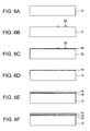
- Fig. 6A through Fig. 6M , Fig. 7A through Fig. 7N , and Fig. 8A through Fig. 8J are views illustrating one example of the manufacturing process for the interposer illustrated in Fig. 5 .
- the process shown in Fig. 6A through Fig. 6M is by and large a process for manufacturing the capacitors 15 on the silicon substrate 12.
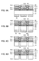
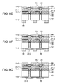
- the process shown in Fig. 7A through Fig. 7N is by and large a process for forming the rewiring layers on the upper side of these capacitors 15.
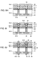
- the process shown in Fig. 8A through Fig. 8J is by and large a process for forming the through-hole conductors 20 on the silicon substrate 12.
- the manufacturing process for the interposer 10 is not limited to this. In the end, any manufacturing method to bring about the interposer 10 such as the one illustrated in Fig. 4 or 5 can be employed.
- Fig. 6A is a step of preparing the silicon (Si) wafer.
- the silicon wafer is of a disk shape being 1 to 3 inches in diameter and 50 to 200 ⁇ m in thickness. This silicon wafer corresponds to the silicon substrate 12 of the interposer 10.
- Fig. 6B is a step of patterning the resist 50 by the lift-off process.
- a dry film is laminated and patterned.
- Fig. 6C is a step of forming the lower electrodes 18 by sputtering.
- a metal layer is deposited by sputtering on the entire surface of the silicon substrate 12 including the top of the resist to form the lower electrodes 18.
- the lower electrodes 18 are preferably formed of platinum (Pt). However, other metals may be used.
- Fig. 6D is a step of stripping the resist 50.
- the resist 50 patterned at the step of Fig. 5B is stripped with a suitable stripping solution. This being the case, the metal layer deposited on the resist is concurrently stripped such that the lower electrodes 18 are patterned.
- Fig. 6E is a step of forming the dielectric layer 16 by sputtering or sol-gel.
- the dielectric layer 16 is made of barium titanate (BaTiOx) having ferroelectricity. To illustrate, it is carried out such that on a magnetron sputter apparatus a target of BaTiOx is placed and the first sputter film of about 0 .
- BaTiOx barium titanate
- a sol-gel film by a sol-gel solution containing barium (Ba) and Titanium (Ti) being spin-coated multiple times on the first sputter film, and, further, that the second sputter film of about 0.15 ⁇ m in film thickness (as with the first sputter film formation) is formed on this spin-coated film.
- the dielectric layer 16 formed accordingly is such that a sol-gel film is interposed between the first sputter film and the second sputter film.
- Fig. 6F is a step of forming the upper electrodes 14 by sputtering.
- the upper electrodes 14 are preferably formed of nickel (Ni). However, other metals may be used.
- Fig. 6G is a step of patterning the resists 52 to be use to form the upper electrodes 14.
- the resists 54 Dry Film Resist AQ series, etc., made by Asahi Kasei Electronics Co., Ltd. of Tokyo, for example, may be used.
- Fig. 6H is a step of etching the upper electrodes 14 and the dielectric layer 16.
- the upper electrodes 14 are formed of nickel (Ni), Item Number Melstrip (mixed acid), for example, made by Meltex Inc. can be used as an etchant.
- Item Number Melstrip mixed acid
- CO2 laser or UV laser can be used.
- Fig. 6I is a step of stripping the resists 52.
- NaOH aqueous solution of about 10% concentration, for example, can be used.
- Fig. 6J is a step of forming the seed layer 54 by sputtering.
- the seed layer 54 nickel (Ni), for example, can be used.
- Fig. 6K is a step of patterning the resists 56 to be use to form the upper electrodes 14.
- the resists 56 Dry Film Resist AQ series, etc., made by Asahi Kasei Electronics Co., Ltd. of Tokyo, Japan, for example, may be used.
- Fig. 6L is a step of etching to form the upper electrodes 14.
- the upper electrodes 14 are formed of nickel (Ni)
- the above-described Item Number Melstrip (mixed acid), for example, is used as an etchant and the nickel (Ni) layer is etched through the opening portions of the resists 56.
- Fig. 6M is a step of stripping the resists 56.
- the above-describe Dry Film Resist AQ series for example, can be used.
- the capacitors 15 can be formed on the silicon substrate 12. Via conductors, through-hole lands, and via lands can also be formed.
- Fig. 7A is a step of forming and patterning the lower side interlaminar insulating resin layer 21-1.
- the lower side interlaminar insulating resin layer 21-1 can be formed of polyimide, for example.
- Fig. 7B is a step of forming by sputtering the seed layer 19-1 on the lower side interlaminar insulating resin layer 21-1patterned.
- nickel (Ni) as the substrate
- copper (Cu) can be used on top thereof.
- Fig. 7C is a step of forming the copper-plated layer 23-1.
- an electrolysis copper plating is formed on the surface of and on the seed layer inside the opening portions of the lower side interlaminar insulating resin layer 21-1 with the seed layer as the electrode.
- the surface of the copper-plated layer 23-1 is smoothened as necessary.
- Fig. 7D is a step of patterning the resist 58.
- the resist 58 is laminated on the copper-plated layer 23-1 to do the patterning.
- the above-described Dry Film Resist AQ series can be used.
- Fig. 7E is a step of etching the copper-plated 23-1 and the seed layer (Cu/Ni) 19-1.
- the copper-plated layer is etched through the opening portions of the resist with the use of hydrogen peroxide/sulfuric acid (H2S04/H202) as an etchant, for example.
- H2S04/H202 hydrogen peroxide/sulfuric acid
- the nickel-plated layer is etched through the opening portions of the resist 58 with the use of the above-described Item Number Melstrip (mixed acid) as an etchant, for example.
- Fig. 7F is a step of stripping the resists 52.
- NaOH aqueous solution of about 10% concentration, for example, can be used.
- Fig. 7G is a step of forming and patterning the upper side interlaminar insulating resin layer 21-2.
- the upper side interlaminar insulating resin layer 21-2 can be formed of polyimide, for example.
- Fig. 7H is a step of forming by sputtering the seed layer 19-2 on the upper side interlaminar insulating resin layer 21-2 patterned.
- the seed layer 19-2 as in the step illustrated in Fig. 7B , with nickel (Ni) as the substrate, copper (Cu) can be used on top thereof.
- Fig. 7I is a step of patterning the resist 60.
- Fig. 7J is a step of forming the copper-plated layer 23-2.
- an electrolysis copper plating is formed on the surface of and on the seed layer 19-2 inside the opening portions of the upper side interlaminar insulating resin layer 21-2 with the seed layer 19-2 as the electrode.
- Fig. 7K is a step of stripping the resists 60.
- NaOH aqueous solution of about 10% concentration, for example, can be used.
- Fig. 7L is a step of etching the copper-plated 23-2 and the seed layer (Cu/Ni) 19-2.
- a copper-plated layer is etched with the use of hydrogen peroxide/sulfuric acid (H2S04/H202) as an etchant and the nickel layer is etched with the use of the above-described Item Number Melstrip (mixed acid), for an example.
- H2S04/H202 hydrogen peroxide/sulfuric acid
- Fig. 7M is a step of patterning the solder resist 38.
- the coating can be done by screen printing with the use of Item Number SR-7200 (photosensitive liquid solder resist) made by Hitachi Chemicals Co., Ltd. of Tokyo, for example.
- Fig. 7N is a step of nickel (Ni)-plating as the undercoat on the copper-plated layer 23-2 and gold (Au)-plating thereon. It is to form the protective layer 24 of the copper-plated layer on the face on which solder bumps are formed to connect to the package.
- the rewiring layers 23-1, 23-2 can be formed on the upper face of the capacitor 15.
- Fig. 8A is a step of patterning the resist 62 on the lower face of the silicon substrate 12.
- the resist 62 is laminated on the lower face of the silicon substrate 12 to do the patterning.
- the above-described Dry Film Resist AQ series can be used, for example.
- Fig. 8B is a step of forming the through holes 12a in the silicon substrate 12.
- the silicon substrate 12 is etched by the anisotropic etching by the RIE process (reactive ion etching) to form the through holes 12a.
- Fig. 8C is a step of stripping the resists 62.
- NaOH aqueous solution of about 10% concentration, for example, can be used.
- Fig. 8D is a step of forming the seed layer 19-3 by sputtering on the silicon substrate 12 having through holes 12a formed.
- copper for example
- an insulating layer SiO2, for example
- the order may be such that at the stage where the lower electrodes 18 are formed on one face of the silicon substrate (see Fig. 6D ) the through holes 12a for through holes are formed (see Fig. 8B ) and that an insulating film of SiO2, etc., is formed on the surface of the silicon substrate including the inner walls of the through holes.
- Fig. 8E is a step of patterning the resist 66.
- a dry film is laminated to do the patterning.
- Fig. 8F is a step of forming the copper-plated layer 23-3.
- an electrolysis copper plating is formed on the surface of and on the seed layer 19-3 inside the opening portions of the silicon substrate 12 with the seed layer 19-3 as the electrode.
- Fig. 8G is a step of stripping the resists 66.
- NaOH aqueous solution of about 10% concentration, for example, can be used.
- Fig. 8H is a step of etching the seed layer 19-3.
- the seed layer 19-3 is formed of copper (Cu)
- the seed layer can be removed by soft etching with the use of hydrogen peroxide/sulfuric acid (H2S04/H202) as an etchant.
- H2S04/H202 hydrogen peroxide/sulfuric acid
- suitable resists may be formed on the copper-plated layer 23-3.
- Fig. 8I is a step of patterning the solder resist 28.
- the coating can be done by screen printing with the use of the above-described Item Number SR-7200 (photosensitive liquid solder resist), for example.
- Fig. 8J is a step of forming the solder bumps 26, 30.
- the solder bumps 26 for the connection to the package are formed, and on the copper-plated layer 23-3 present in the opening portions 28a of the solder resist 28, the solder bumps 30 for the connection to the IC chip are formed.
- the solder bumps 26, 30 can be formed by screen printing, for example.
- interposers illustrated in Fig. 4 can be manufactured by using a portion of the above-described steps (e.g., Figs. 6A through 6M , Fig. 7A through Fig. 7F , 8A through 8J ).
- the interposer illustrated 10 in Fig. 4 is interposed between the IC chip 40 and the package substrate 42 such that it is mutually connected to them separately, constituting an electronic device 70-1 comprising a combination of a semiconductor chip, an interposer, and a package substrate.
- This electronic device 70-1 is formed, following the manufacture of the interposer 10, by reflowing the solder bumps 26, 30 such that the interposer 10 is solder-connected to the semiconductor chip 40 and the package substrate 42 separately.
- the interposer 10 is positioned near the semiconductor 40 and functions as a decoupling capacitor having a large capacity.
- the interposer illustrated 10 in Fig. 5 is interposed between the IC chip 40 and the package substrate 42 such that it is mutually connected to them separately, constituting an electronic device 70-2 comprising a combination of a semiconductor chip, an interposer, and a package substrate.
- This electronic device 7-2 is formed, following the manufacture of the interposer 10, by reflowing the solder bumps 26, 30 such that the interposer 10 is solder-connected to the semiconductor chip 40 and the package substrate 42 separately.
- the interposer 10 provides the rewiring layers 23-1, 23-2 between the semiconductor chip 40 and the package substrate 42.
- the interposers 10 pertaining to the present embodiments are such that since there are present no rewiring patterns occupying the surface of the silicon substrate 12, the capacitor electrodes having a large area can be formed.
- the interposers 10 pertaining to the present embodiments can form the dielectric layer very thin, namely, the gap between the upper electrodes 14 and the lower electrodes 18 very narrow since a silicon substrate having an extremely smooth surface is used. It results in the capacitor formed on the substrate having a large capacity.
- the interposers 10 pertaining to the present embodiments can form a decoupling capacitor having a large capacity on the substrate since a substance having ferroelectricity such as a barium titanate (BaTiO3) layer can be employed.
- a substance having ferroelectricity such as a barium titanate (BaTiO3) layer can be employed.
- the electronic devices 70-1 pertaining to the present embodiments can further provide decoupling capacitors having a large capacity extremely near to the semiconductor chip 40 on account of the combination of the semiconductor chip 40, the interposer 10, and a package substrate 42.
- the electronic devices 70-2 pertaining the present embodiments can provide, while positioning a decoupling capacitor having a large capacity extremely near to the semiconductor chip 40, the rewiring layers 23-1, 23-2.
- the through-hole conductors 20 and the via conductors 22 are longitudinally connected, and generally referred to as through-hole conductors and via conductors 20, 22.
- the through-hole conductors 20 may be such that they are not connected to the lower electrodes 18 by the clearance 25 and that they are connected to the upper electrodes 14 being positioned away from them via the via conductors 22.
- the through-hole conductors 20 and via conductors 22 are, while they are electrically connected, not connected longitudinally.
- Such a set-up may be applicable to either the through-hole conductors for power supply, ground, and signal or the via conductors. Therefore, the technical scope of the present invention is set forth in accordance with the description of the accompanying claims.
Landscapes
- Engineering & Computer Science (AREA)
- Microelectronics & Electronic Packaging (AREA)
- Production Of Multi-Layered Print Wiring Board (AREA)
- Semiconductor Integrated Circuits (AREA)
- Internal Circuitry In Semiconductor Integrated Circuit Devices (AREA)
- Fixed Capacitors And Capacitor Manufacturing Machines (AREA)
Abstract
Provided are a novel interposer and a method for manufacturing such interposer. The interposer (10) is provided with a silicon substrate (12); a plurality of through hole conductors (20) formed on the silicon substrate; and a capacitor (15) composed of an upper electrode (14) and a lower electrode (18) formed by extending the land portions of the through hole conductors, and a dielectric layer (16) formed between the electrodes. Rewiring layers (23-1, 23-2) are formed as needed on a layer different from the capacitor.
Description
- The present invention relates to an interposer and an electronic device using the same, and, more specifically, to an interposer interposed between a semiconductor chip and a package substrate as well as to an electronic device composed of a combination of the conductor chip, the interposer, and the package substrate.
- There has conventionally been known an interposer as a printed wiring board for carrying out rewiring between a semiconductor chip and a package substrate. An interposer is mainly a rewiring device used to mutually connect a conductor circuit having an ultra dense pitch (e.g., 50µm) of a semiconductor chip and a conductor circuit having a more coarse pitch (e.g., 150µm) of a package substrate (also referred to as a "mounting substrate").
- Patent Document 1: Laid-Open Patent No.
2001-326305 "Interposer for Semiconductor Device, Method of Manufacturing the Same, and Semiconductor Device" (Laid-open, unexamined, November 22, 2001)
The above-described patent document discloses an interposer wherein a capacitor and a wiring pattern are formed on an insulating substrate. - The studies undertaken subsequently by the present inventor found that various problems would occur when a capacitor and a rewiring layer are formed together on an interposer as described in the patent document 1.
- Accordingly, the purpose of the present invention is to provide a novel interposer and an electronic device using it.
- In view of the above-described purpose, the interposer pertaining to the present invention comprises a capacitor formed on nearly the entire surface of the substrate.
- Further, in the above-described interposer, the above-described capacitor comprises a lower electrodes having opening portions, a dielectric layer formed on the above-described lower electrodes, and upper electrodes formed on the above-described dielectric layer and having opening portions, and the above-describe interposer further has through-hole conductors for power supply running through the above-described substrate and electrically connected to the power supply electrodes of the IC chip, through-hole lands for power supply connected to the above-described through-hole conductors for power supply and formed inside the opening portions of the above-described lower electrodes, through-hole conductors for ground running through the above-described substrate and electrically connected to the ground electrodes of the IC chip, via lands for ground electrically connected to the above-described through holes for ground and formed inside the opening portions of the above-described upper electrodes, through-hole conductors for signal running through the above-described substrate and electrically connected to the signal electrodes of the IC chip, through-hole lands connected to the above-described through-hole conductors for signal and formed on the above-described substrate, via conductors for ground connecting the above-described via lands for ground and the above-described lower electrodes and formed on the above-described dielectric layer, and via conductors for power supply connecting the above-described through-hole lands for power supply and the upper electrodes and formed on the above-described dielectric layer, and the above-described through-hole conductors for signal may be formed in the regions other than the regions where the above-described through-hole conductors for ground and the above-described through-hole conductors for power supply are formed.
- Further, in the above-described interposer, the above-described capacitor comprises lower electrodes having opening portions, a dielectric layer formed on the above-described lower electrodes, and upper electrodes formed on the above-described dielectric layer and having opening portions, and the above-describe interposer further has through-hole conductors for ground running through the above-described substrate and electrically connected to the ground electrodes of the IC chip, through-hole lands for ground connected to the above-described through-hole conductors for ground and formed inside the opening portions of the above-described lower electrodes, through-hole conductors for power supply running through the above-described substrate and electrically connected to the power supply electrodes of the IC chip, via lands for power supply electrically connected to the above-described through hole conductors for power supply and formed inside the opening portions of the above-described upper electrodes, through-hole conductors for signal running through the above-described substrate and electrically connected to the signal electrodes of the IC chip, through-hole lands for signal connected to the above-described through-hole conductors for signal and formed on the above-described substrate, via conductors for power supply connecting the above-described via lands for power supply and the above-described lower electrodes and formed on the above-described dielectric layer, and via conductors for ground connecting the above-described through-hole lands for ground and the upper electrodes and formed on the above-described dielectric layer, and the above-described through-hole conductors for signal may be formed in the regions other than the regions where the above-described through-hole conductors for ground and the above-described through-hole conductors for power supply are formed.
- Further, an electronic device pertaining to the present invention comprises an IC chip, a package substrate, an interposer interposed between the above-described IC chip and the above-described package substrate and electrically connected to the both separately and as set forth in claims 1-2, and the above-described interposer provides a capacitor.
- Further, the method of manufacturing an interposer pertaining to the present invention is set forth such that a silicon substrate being prepared, a capacitor comprising lower electrodes, a dielectric layer , and upper electrodes is formed on nearly the entire face of one face of the above-described silicon substrate, that through holes are formed into said silicon substrate from the other face of the above-described silicon substrate, that through-hole conductors are formed inside the above-described through holes, that some of the above-described through-hole conductors are electrically connected to the above-described lower electrodes, and that some of the remainder of the above-described through-hole conductors are connected to the above-described upper electrodes via via-hole conductors formed on the above-described dielectric layer.
- Further, the method of manufacturing an electronic device pertaining to the present invention is a method set forth such that an interposer manufactured in accordance with the above-described method being prepared, an IC chip is electrically connected to one face of the above-described interposer and a package is electrically connected to the other face of the above-described interposer.
- The present invention can provide a novel interposer and an electronic device using it.
-
-
Fig. 1 is a sectional view illustrating the feature of an interposer pertaining to the present embodiment. -
Fig. 2 is a view of a portion of the capacitor formed on the interposer illustrated inFig. 1 as viewed from the lower electrodes side. -
Fig. 3 is a sectional view illustrating the feature of an interposer pertaining to another embodiment. -
Fig. 4 is a sectional view illustrating the constitution of an electronic device using an interposer. -
Fig. 5 is a sectional view illustrating the constitution of an electronic device using another interposer. -
Fig. 6A through Fig. 6M are views illustrating an example of the manufacturing process of an interposer illustrated inFig. 5 , generally speaking, a step for forming a capacitor on a silicon substrate. -
Fig. 7A through Fig. 7N are views illustrating an example of the manufacturing process of an interposer illustrated inFig. 5 , generally speaking, a step for forming a rewiring layer on the upper face of this capacitor. -
Fig. 8A through Fig. 8J are views illustrating an example of the manufacturing process of an interposer illustrated inFig. 5 , generally speaking, a step for forming through-hole conductors on a silicon substrate. - 10:interposer, 12:silicon substrate, 12a:through hole, 14:upper electrode, 15:capacitor, 16:dielectric layer, 18:lower electrode, 20-1:through-hole conductor, through-hole conductors for signal, 20-2:through-hole conductor, through-hole conductor for power supply, 20-3: through-hole conductor, through-hole conductor for ground, 22-1 :via conductor, via conductors for signal, 22-2: via conductor, via conductors for power supply, 22-3:via conductor, via conductors for ground, 21-1:lower side interlaminar insulating resin layer, 21-2:upper side interlaminar insulating resin layer, 23-1,23-2,23-3:rewiring layer, copper plated layer, 24:clearance, 25:clearance, 26:solder bump, 28:solder resist layer, 28a:opening, 30:solder bump, 38:solder resist layer, 40:semiconductor chip, IC chip, 42:package substrate, 50,56,58,62,66:resist, 62a:opening, 100:opening portion, 70-1,70-2:electronic device, 101:opening portion, 102:through-hole land,
- The following is a brief description of the embodiments of a novel interposer and an electronic device using this pertaining to the present invention with reference to the accompanying drawings. It should be understood that these embodiments are for the illustrative purpose and that the present invention is not limited thereto. In addition, the same components are denoted by the same reference numerals in the drawings, and duplicate explanations are omitted.
-
Fig. 1 is a sectional view illustrating the feature of aninterposer 10 pertaining to the present embodiment. Theinterposer 10 comprises through-hole conductors 20-1, 20-2, 20-3 formed on thesilicon substrate 12 and via conductors 22-2, 22-3 formed on thedielectric layer 16. The through-hole conductors 20-1 through 20-3 are connected to either through-hole lands 102 formed on the substrate surface or to thelower electrodes 18. The via conductors 22-1 through 22-3 are connected to thevia lands 103 formed on thedielectric layer 16. The through-hole conductors for power supply 20-2 and the via conductors for power supply 22-2 are longitudinally connected, and, likewise, the through-hole conductors for ground 20-3 and the via conductors for ground 22-3 as well as the through-hole conductors for signal 20-1 and the via conductors for signal 22-1 (seeFig. 3 ) are longitudinally connected, respectively. Therefore, in the present application document, the through holes and the via holes being longitudinally connected may generally be referred to with a general term such as "through-hole conductors and via conductors 20-1, 22-1." Theinterposer 10 comprises thissilicon substrate 12 and acapacitor 15 comprisinglower electrodes 18 havingopening portions 101, adielectric layer 16, andupper electrodes 14 having theopening portions 100. - The
clearances hole lands 102 and vialands 103, respectively, and theopening portions hole lands 102 and vialands 103 are formed, respectively. - Via conductors for power supply 22-2 need not be formed directly above through-hole conductors for power supply 20-2. And, the number of through-hole conductors for power supply and the number of via conductors for power supply need not be the same. The less the number of via conductors for power supply is, the less the number of the
opening portions 100 provided on theupper electrodes 14 can be. - Via conductors for ground 22-3 need not be formed directly above through-hole conductors for ground 20-3. And, the number of through-hole conductors for ground and the number of via conductors for ground need not be the same. The less the number of via conductors for ground is, the less the number of the
opening portions 101 provided on thelower electrodes 18 can be. - When the surface of the
silicon substrate 12 is properly polished, it has a property such that the surface is extremely smooth. In addition, if the surface smoothness level required in the present embodiment is satisfied, a glass substrate or a polyimide substrate may be used in lieu of a silicon substrate. - The through-hole conductors and via conductors 20-1, 22-1 of the interposer 10 (see
Fig. 3 ) are conductors for signal, transmitting signals between a semiconductor chip (seeFigs. 4 and5 ) and a package substrate (seeFigs. 4 and5 ), as described below. - The through-hole conductors for ground 20-3 are connected to the through-
hole lands 102 formed in theopening portions 101 of thelower electrodes 18, and, further, connected to theupper electrodes 14 via via conductors for ground 22-3. The through-hole lands 102 are insulated from thelower electrodes 18 by theclearances 25. The through-hole conductors for power supply 20-2 are connected to thelower electrodes 18, and, further, to thevia lands 103 provided in theopening portions 100 of theupper electrodes 14 via the via conductors for power supply 22-2. And thevia lands 103 and theupper electrodes 14 are insulated from each other by theclearance 24. - And, alternately, the through-hole conductors for power supply 20-2 are connected to the through-
hole lands 102 formed in theopening portions 101 of thelower electrodes 18, and, further, may be connected to theupper electrodes 14 via via conductors for power supply 22-2. And the through-hole conductors 20-3 are connected to thelower electrodes 18, and, further, may be connected to thevia lands 103 provided in theopening portions 100 of theupper electrodes 14. - The
upper electrodes 14 and thelower electrodes 18 are formed of suitable metals. In the present embodiment, theupper electrodes 14 are formed of nickel (Ni), for example, and thelower electrodes 18 are formed of platinum (Pt), for example, for the convenience of production. However, they may be formed of other metals. - The
dielectric layer 16 is preferably of a high dielectric substance. Thedielectric layer 16 is formed of barium titanate (BaTi03) having ferroelectricity, for example. - Here, the
upper electrodes 14, thedielectric layer 16, and thelower electrodes 18 form thecapacitor 15. - The
interposer 10 illustrated inFig. 1 is placed, as described below, between a semiconductor chip (seeFigs. 4 and5 ) and a package substrate (also referred to as a "mounting substrate") (seeFigs. 4 and5 ). Theinterposer 10 is placed very close to the semiconductor chip to form a decoupling capacitor between a power supply and the ground to absorb noise. - The
interposer 10 illustrated inFig. 1 is such that thedielectric layer 16 is formed on nearly the entire face of one face of thesilicon substrate 12 such that the conductor layers on both faces interposing this dielectric layer constitute the upper andlower electrodes - The
interposer 10 illustrated inFig. 1 does not have the signal wiring in the regions in which thecapacitor 15 is formed. Accordingly, the electrodes for thecapacitors silicon substrate 12 to have a large area can be formed. - Since the surface of the
interposer 10 illustrated inFig. 1 is extremely smooth, thedielectric layer 16 can be formed very thin, namely, theupper electrodes 14 and thelower electrodes 18 can be formed such that the gap therebetween is very narrow. - For the
dielectric layer 16 used for theinterposer 10 illustrated inFig. 1 , a barium titanate (BaTiO3) layer being of ferroelectricity can be used. - The
interposer 10 illustrated inFig. 1 can, by employing at least one of these features, form a capacitor (condenser) having a very large capacity. -
Fig. 2 is a view of a portion of thecapacitor 15 formed on theinterposer 10 illustrated inFig. 1 as viewed from the side of thelower electrodes 18. InFig. 2 the area shown in white illustrates thelower electrodes 18 and the box shapes shown in black illustrate thedielectric layer 16 seen from the opening portions of thelower electrodes 18. It shows that the lower electrodes are formed on nearly the entire face of the silicon substrate area. -
Fig. 3 is a sectional view illustrating a feature of an interposer pertaining to another embodiment. As to the feature of the interposer in the above-describedFig. 1 , the through-hole conductors for signal and via conductors for signal 20-1, 22-1 are disposed on a peripheral region of thesilicon substrate 12 and the through-hole conductors for power supply and via conductors for power supply 20-2, 22-2 as well as the through-hole conductors for ground and via conductors for ground 20-3, 22-3 being disposed on the central region of thesilicon substrate 12 to form thecapacitors 15. As opposed to this, the feature of the interposer illustrated inFig. 3 differs in that the through-hole conductors for signal and via conductors for signal 20-1, 22-1 are disposed such that they are concentrated on the central region while the through-hole conductors for power supply and via conductors for power supply 20-2, 22-2 as well as the through-hole conductors for ground and via conductors for ground 20-3, 22-3 are disposed on the peripheral region such that they surround them. - As illustrated in
Fig. 3 , as to the via conductors for power supply 22-2, the land portions thereof extend to form theupper electrodes 14. And, the through-hole lands 102 are formed in the openingportions 101 of thelower electrodes 18 and insulated from thelower electrodes 18 by theclearance 25. The through-hole conductors for signal and via conductors 20-1, 22-1 are insulated from theupper electrodes 14 by theclearances 24 and insulated from thelower electrodes 18 by theclearance 25. As to the through-hole conductors for ground 20-3, the land portions thereof extend to form thelower electrodes 18, and are being disconnected from theupper electrodes 14. They are electrically being disconnected from the upper electrodes I by via conductors connected to theupper electrodes 14 not being formed, for example, or by theclearance 24 by vialands 103 being formed in the openingportions 100 of theupper electrodes 14. - In addition, the through-hole conductors and via conductors for signal 20-1, 22-1, the through-hole conductors and via conductors for power supply 20-2, 22-2, and the through-hole conductors and via conductors for ground 20-3, 22-3 may be disposed in mixture.
-
Fig. 4 is a sectional view illustrating the constitution of an electronic device using theinterposer 10. Theinterposer 10 is interposed between the IC chip (IC) 40 and the package substrate (PK) 42 and is solder-connected to theIC chip 40 through thesolder bump 26 and to thepackage substrate 42 through thesolder bump 30, respectively. - The
interposer 10 illustrated inFig. 4 comprises, in addition to theupper electrodes 14, thedielectric layer 16, thelower electrodes 18, thesilicon substrate 12, and the through-hole conductors and viaconductors Figs. 1 and3 , the insulatingresin layer 21 formed on theupper electrodes 14, the nickel (Ni) lands connected to the through-hole conductors via the opening portions of this insulating resin layer, the gold (Au)-plated layer 24-2 covering these nickel lands (pads), the solder bumps formed on the gold-plated layer, the solder resistlayer 28 formed on the lower face of thesilicon substrate 12 and the solder bumps 30 formed on the land (external electrodes) portions of the through-hole conductors 20 via the opening portions of this solder resist layer. - The
interposer 10 inFig. 4 is such that since thecapacitor 15 is placed very close to thesemiconductor chip 40, a decoupling capacitor can be formed between a power supply and the ground to absorb noise. - The
interposer 10 inFig. 4 is such that since there are present no rewiring patterns occupying the surface of thesilicon substrate 12, thecapacitor electrodes - The
interposer 10 inFig. 4 is such that since the surface of thesilicon substrate 12 is extremely smooth, the gap between theupper electrodes 14 and thelower electrodes 18 can be made very narrow. - The
interposer 10 inFig. 4 is such that since a dielectric substance having ferroelectricity can be employed as thedielectric layer 16, a capacitor (condenser) having a very large capacity can be formed. -
Fig. 5 is a sectional view illustrating the constitution of an electronic device using anotherinterposer 10. The constitution of the interposer illustrated inFig. 5 differs, as compared to that inFig. 4 , in that rewiring layers 23-1, 23-2 are added. - The
interposer 10 illustrated inFig. 4 comprises, in addition to theupper electrodes 14, thedielectric layer 16, thelower electrodes 18, thesilicon substrate 12, the through-hole conductors 20, viaconductors 22, the solder bumps 26, the solder resistlayer 28, and the solder bumps 30, as described in conjunction withFig. 4 , the lower side interlaminar insulating resin layer 21-1 whereon the rewiring pattern 23-1 is formed, the upper side interlaminar insulating resin layer 21-2 whereon the rewiring pattern 23-2 is formed, and the solder resistlayer 38. The lower side interlaminar insulating resin layer 21-1 is formed on the capacitor. The rewiring pattern 23-1 formed on the lower side interlaminar insulating resin layer is connected to either of the through-hole conductors for signal 20-1, the through-hole conductors for power supply 20-2, and the through-hole conductors for ground 20-3 via the via-hole conductors 22 formed on the lower side interlaminar insulating layer. The interlaminar layers may be one layer or a plurality of layers. - However, these rewiring patterns 23-1, 23-2 are formed on the layers other than the capacitor (namely, the interlaminar insulating resin layers 21-1, 21-2) respectively. That is, there are no rewiring patterns present in the
capacitors 15 comprising theupper electrodes 14, thedielectric layer 16, and thelower electrodes 18. Accordingly, capacitor electrodes having a large area can still be formed. - Therefore, the
interposer 10 illustrated inFig. 5 possesses the functions and features of the interposer described in conjunction withFig. 1 andFig. 3 . Theinterposer 10 inFig. 5 is such that since it is placed very close to thesemiconductor chip 40, in addition to the interconnection function between thesemiconductor chip 40 and thepackage substrate 42, a decoupling capacitor can be formed between a power supply and the ground to absorb noise. - The
interposer 10 inFig. 5 is such that since no rewiring patterns are present on the portions of thecapacitor 15, the capacitor electrodes having a large area can be formed. - The
interposer 10 inFig. 5 is such that thecapacitor 15 is formed on thesilicon substrate 12 having a very smooth surface. The thickness of the dielectric layer can be made very thin. - The
interposer 10 inFig. 5 is such that since a dielectric substance having ferroelectricity can be employed as thedielectric layer 16, a capacitor (condenser) having a very large capacity can be formed. -
Fig. 6A through Fig. 6M ,Fig. 7A through Fig. 7N , andFig. 8A through Fig. 8J are views illustrating one example of the manufacturing process for the interposer illustrated inFig. 5 . Here, the process shown inFig. 6A through Fig. 6M is by and large a process for manufacturing thecapacitors 15 on thesilicon substrate 12. The process shown inFig. 7A through Fig. 7N is by and large a process for forming the rewiring layers on the upper side of thesecapacitors 15. Further, the process shown inFig. 8A through Fig. 8J is by and large a process for forming the through-hole conductors 20 on thesilicon substrate 12. However, the manufacturing process for theinterposer 10 is not limited to this. In the end, any manufacturing method to bring about theinterposer 10 such as the one illustrated inFig. 4 or5 can be employed. -
Fig. 6A is a step of preparing the silicon (Si) wafer. To give an example, the silicon wafer is of a disk shape being 1 to 3 inches in diameter and 50 to 200µm in thickness. This silicon wafer corresponds to thesilicon substrate 12 of theinterposer 10. -
Fig. 6B is a step of patterning the resist 50 by the lift-off process. To give an example, on the upper face of thesilicon substrate 12 a dry film is laminated and patterned. -
Fig. 6C is a step of forming thelower electrodes 18 by sputtering. A metal layer is deposited by sputtering on the entire surface of thesilicon substrate 12 including the top of the resist to form thelower electrodes 18. Thelower electrodes 18 are preferably formed of platinum (Pt). However, other metals may be used. -
Fig. 6D is a step of stripping the resist 50. The resist 50 patterned at the step of Fig. 5B is stripped with a suitable stripping solution. This being the case, the metal layer deposited on the resist is concurrently stripped such that thelower electrodes 18 are patterned. -
Fig. 6E is a step of forming thedielectric layer 16 by sputtering or sol-gel. Thedielectric layer 16 is made of barium titanate (BaTiOx) having ferroelectricity. To illustrate, it is carried out such that on a magnetron sputter apparatus a target of BaTiOx is placed and the first sputter film of about 0.25µm in film thickness is formed, that there is formed a sol-gel film by a sol-gel solution containing barium (Ba) and Titanium (Ti) being spin-coated multiple times on the first sputter film, and, further, that the second sputter film of about 0.15µm in film thickness (as with the first sputter film formation) is formed on this spin-coated film. Thedielectric layer 16 formed accordingly is such that a sol-gel film is interposed between the first sputter film and the second sputter film. -
Fig. 6F is a step of forming theupper electrodes 14 by sputtering. Theupper electrodes 14 are preferably formed of nickel (Ni). However, other metals may be used. -
Fig. 6G is a step of patterning the resists 52 to be use to form theupper electrodes 14. As for the resists 54, Dry Film Resist AQ series, etc., made by Asahi Kasei Electronics Co., Ltd. of Tokyo, for example, may be used. -
Fig. 6H is a step of etching theupper electrodes 14 and thedielectric layer 16. When theupper electrodes 14 are formed of nickel (Ni), Item Number Melstrip (mixed acid), for example, made by Meltex Inc. can be used as an etchant. When through holes are formed in thedielectric layer 16, CO2 laser or UV laser can be used. -
Fig. 6I is a step of stripping the resists 52. For a resist stripper, NaOH aqueous solution of about 10% concentration, for example, can be used. -
Fig. 6J is a step of forming the seed layer 54 by sputtering. As the seed layer 54, nickel (Ni), for example, can be used. -
Fig. 6K is a step of patterning the resists 56 to be use to form theupper electrodes 14. As for the resists 56, Dry Film Resist AQ series, etc., made by Asahi Kasei Electronics Co., Ltd. of Tokyo, Japan, for example, may be used. -
Fig. 6L is a step of etching to form theupper electrodes 14. When theupper electrodes 14 are formed of nickel (Ni), the above-described Item Number Melstrip (mixed acid), for example, is used as an etchant and the nickel (Ni) layer is etched through the opening portions of the resists 56. -
Fig. 6M is a step of stripping the resists 56. For a resist stripper, the above-describe Dry Film Resist AQ series, for example, can be used. Through the steps illustrated in theseFig. 6A through Fig. 6M , thecapacitors 15 can be formed on thesilicon substrate 12. Via conductors, through-hole lands, and via lands can also be formed. -
Fig. 7A is a step of forming and patterning the lower side interlaminar insulating resin layer 21-1. The lower side interlaminar insulating resin layer 21-1 can be formed of polyimide, for example. -
Fig. 7B is a step of forming by sputtering the seed layer 19-1 on the lower side interlaminar insulating resin layer 21-1patterned. For the see layer 19-1, with nickel (Ni) as the substrate, copper (Cu) can be used on top thereof. -
Fig. 7C is a step of forming the copper-plated layer 23-1. For the copper-plated layer 23-1, an electrolysis copper plating is formed on the surface of and on the seed layer inside the opening portions of the lower side interlaminar insulating resin layer 21-1 with the seed layer as the electrode. The surface of the copper-plated layer 23-1 is smoothened as necessary. -
Fig. 7D is a step of patterning the resist 58. To etch the copper-plated layer 23-1, the resist 58 is laminated on the copper-plated layer 23-1 to do the patterning. For the resist 58, the above-described Dry Film Resist AQ series can be used. -
Fig. 7E is a step of etching the copper-plated 23-1 and the seed layer (Cu/Ni) 19-1. When etching a copper-plated layer and the copper layer of a seed layer, the copper-plated layer is etched through the opening portions of the resist with the use of hydrogen peroxide/sulfuric acid (H2S04/H202) as an etchant, for example. When etching the nickel layer of a seed layer, the nickel-plated layer is etched through the opening portions of the resist 58 with the use of the above-described Item Number Melstrip (mixed acid) as an etchant, for example. -
Fig. 7F is a step of stripping the resists 52. For a resist stripper, NaOH aqueous solution of about 10% concentration, for example, can be used. -
Fig. 7G is a step of forming and patterning the upper side interlaminar insulating resin layer 21-2. As with the step of forming the lower side insulating resin layer 21-1 as illustrated inFig. 6D , the upper side interlaminar insulating resin layer 21-2 can be formed of polyimide, for example. -
Fig. 7H is a step of forming by sputtering the seed layer 19-2 on the upper side interlaminar insulating resin layer 21-2 patterned. For the see layer 19-2, as in the step illustrated inFig. 7B , with nickel (Ni) as the substrate, copper (Cu) can be used on top thereof. -
Fig. 7I is a step of patterning the resist 60. -
Fig. 7J is a step of forming the copper-plated layer 23-2. For the copper-plated layer 23-2, an electrolysis copper plating is formed on the surface of and on the seed layer 19-2 inside the opening portions of the upper side interlaminar insulating resin layer 21-2 with the seed layer 19-2 as the electrode. -
Fig. 7K is a step of stripping the resists 60. For a resist stripper, NaOH aqueous solution of about 10% concentration, for example, can be used. -
Fig. 7L is a step of etching the copper-plated 23-2 and the seed layer (Cu/Ni) 19-2. As in the step illustrated inFig. 7E , a copper-plated layer is etched with the use of hydrogen peroxide/sulfuric acid (H2S04/H202) as an etchant and the nickel layer is etched with the use of the above-described Item Number Melstrip (mixed acid), for an example. -
Fig. 7M is a step of patterning the solder resist 38. For the solder resist 38, the coating can be done by screen printing with the use of Item Number SR-7200 (photosensitive liquid solder resist) made by Hitachi Chemicals Co., Ltd. of Tokyo, for example. -
Fig. 7N is a step of nickel (Ni)-plating as the undercoat on the copper-plated layer 23-2 and gold (Au)-plating thereon. It is to form theprotective layer 24 of the copper-plated layer on the face on which solder bumps are formed to connect to the package. By theseFig. 7A through Fig. 7N , the rewiring layers 23-1, 23-2 can be formed on the upper face of thecapacitor 15. -
Fig. 8A is a step of patterning the resist 62 on the lower face of thesilicon substrate 12. To form the throughholes 12a in thesilicon substrate 12, the resist 62 is laminated on the lower face of thesilicon substrate 12 to do the patterning. For the resist 62, the above-described Dry Film Resist AQ series can be used, for example. -
Fig. 8B is a step of forming the throughholes 12a in thesilicon substrate 12. Through the openingportions 62a formed in the resist 62, thesilicon substrate 12 is etched by the anisotropic etching by the RIE process (reactive ion etching) to form the throughholes 12a. -
Fig. 8C is a step of stripping the resists 62. For a resist stripper, NaOH aqueous solution of about 10% concentration, for example, can be used. -
Fig. 8D is a step of forming the seed layer 19-3 by sputtering on thesilicon substrate 12 having throughholes 12a formed. For the seed layer 19-3, copper (Cu), for example, can be used. Prior to the formation of the seed layer, an insulating layer (SiO2, for example) is formed on the surface of the silicon substrate by CVD method, etc. In addition, as to the order of manufacturing steps, the order may be such that at the stage where thelower electrodes 18 are formed on one face of the silicon substrate (seeFig. 6D ) the throughholes 12a for through holes are formed (seeFig. 8B ) and that an insulating film of SiO2, etc., is formed on the surface of the silicon substrate including the inner walls of the through holes. -
Fig. 8E is a step of patterning the resist 66. On the seed layer 19-3 of the surface of thesilicon substrate 12, a dry film is laminated to do the patterning. -
Fig. 8F is a step of forming the copper-plated layer 23-3. For the copper-plated layer 23-3, an electrolysis copper plating is formed on the surface of and on the seed layer 19-3 inside the opening portions of thesilicon substrate 12 with the seed layer 19-3 as the electrode. -
Fig. 8G is a step of stripping the resists 66. For a resist stripper, NaOH aqueous solution of about 10% concentration, for example, can be used. -
Fig. 8H is a step of etching the seed layer 19-3. When the seed layer 19-3 is formed of copper (Cu), for example, the seed layer can be removed by soft etching with the use of hydrogen peroxide/sulfuric acid (H2S04/H202) as an etchant. In addition, upon etching, suitable resists may be formed on the copper-plated layer 23-3. -
Fig. 8I is a step of patterning the solder resist 28. For the solder resist 28, the coating can be done by screen printing with the use of the above-described Item Number SR-7200 (photosensitive liquid solder resist), for example. -
Fig. 8J is a step of forming the solder bumps 26, 30. On the copper-plated layer 23-2 present in the opening portions 38a of the solder resist 38, the solder bumps 26 for the connection to the package are formed, and on the copper-plated layer 23-3 present in the opening portions 28a of the solder resist 28, the solder bumps 30 for the connection to the IC chip are formed. The solder bumps 26, 30 can be formed by screen printing, for example. By theseFig.8A through Fig. 8J , the through-hole conductors 20 can be formed in thesilicon substrate 12. - In addition, the interposers illustrated in
Fig. 4 can be manufactured by using a portion of the above-described steps (e.g.,Figs. 6A through 6M ,Fig. 7A through Fig. 7F ,8A through 8J ). - The interposer illustrated 10 in
Fig. 4 is interposed between theIC chip 40 and thepackage substrate 42 such that it is mutually connected to them separately, constituting an electronic device 70-1 comprising a combination of a semiconductor chip, an interposer, and a package substrate. - This electronic device 70-1 is formed, following the manufacture of the
interposer 10, by reflowing the solder bumps 26, 30 such that theinterposer 10 is solder-connected to thesemiconductor chip 40 and thepackage substrate 42 separately. Theinterposer 10 is positioned near thesemiconductor 40 and functions as a decoupling capacitor having a large capacity. - The interposer illustrated 10 in
Fig. 5 is interposed between theIC chip 40 and thepackage substrate 42 such that it is mutually connected to them separately, constituting an electronic device 70-2 comprising a combination of a semiconductor chip, an interposer, and a package substrate. This electronic device 7-2 is formed, following the manufacture of theinterposer 10, by reflowing the solder bumps 26, 30 such that theinterposer 10 is solder-connected to thesemiconductor chip 40 and thepackage substrate 42 separately. Theinterposer 10 provides the rewiring layers 23-1, 23-2 between thesemiconductor chip 40 and thepackage substrate 42. - The
interposers 10 pertaining to the present embodiments are such that since there are present no rewiring patterns occupying the surface of thesilicon substrate 12, the capacitor electrodes having a large area can be formed. - The
interposers 10 pertaining to the present embodiments can form the dielectric layer very thin, namely, the gap between theupper electrodes 14 and thelower electrodes 18 very narrow since a silicon substrate having an extremely smooth surface is used. It results in the capacitor formed on the substrate having a large capacity. - The
interposers 10 pertaining to the present embodiments can form a decoupling capacitor having a large capacity on the substrate since a substance having ferroelectricity such as a barium titanate (BaTiO3) layer can be employed. - The electronic devices 70-1 pertaining to the present embodiments can further provide decoupling capacitors having a large capacity extremely near to the
semiconductor chip 40 on account of the combination of thesemiconductor chip 40, theinterposer 10, and apackage substrate 42. - The electronic devices 70-2 pertaining the present embodiments can provide, while positioning a decoupling capacitor having a large capacity extremely near to the
semiconductor chip 40, the rewiring layers 23-1, 23-2. - In the above, the embodiments of the interposers and of the electronic devices using it pertaining to the present invention were described, and these are only examples and the present invention is not limited thereto.
For example, the through-hole conductors 20 and the viaconductors 22 are longitudinally connected, and generally referred to as through-hole conductors and viaconductors Fig. 1 andFig. 3 , the through-hole conductors 20 may be such that they are not connected to thelower electrodes 18 by theclearance 25 and that they are connected to theupper electrodes 14 being positioned away from them via the viaconductors 22. In this case, the through-hole conductors 20 and viaconductors 22 are, while they are electrically connected, not connected longitudinally. Such a set-up may be applicable to either the through-hole conductors for power supply, ground, and signal or the via conductors.
Therefore, the technical scope of the present invention is set forth in accordance with the description of the accompanying claims.
Claims (17)
- An interposer comprising a capacitor formed on nearly the entire face of the surface of a substrate.
- The interposer as set forth in claim 1, comprising:the above-described capacitor comprising lower electrodes having opening portions, a dielectric layer formed on the above-described lower electrodes, and upper electrodes formed on the above-described dielectric layer and having opening portions; andthe above-describe interposer further having;through-hole conductors for power supply running through the above-described substrate and electrically connected to the power supply electrodes of the IC chip;through-hole lands for power supply connected to the above-described through-hole conductors for power supply and formed inside the opening portions of the above-described lower electrodes;through-hole conductors for ground running through the above-described substrate and electrically connected to the ground electrodes of the IC chip;via lands for ground electrically connected to the above-described through-hole conductors for ground and formed inside the opening portions of the above-described upper electrodes;through-hole conductors for signal running through the above-described substrate and electrically connected to the signal electrodes of the IC chip;through-hole lands for signal connected to the above-described through-hole conductors for signal and formed on the above-described substrate;via conductors for ground connecting the above-described via lands for ground and the above-described lower electrodes and formed on the above-described dielectric layer; andvia conductors for power supply connecting the above-described through-hole lands for power supply and the upper electrodes and formed on the above-described dielectric layer, andthe above-described through-hole conductors for signal being formed in the areas other than the areas where the above-described through-hole conductors for ground and the above-described through-hole conductors for power supply being formed.
- The interposer as set forth in claim 1, comprising:the above-described capacitor comprising lower electrodes having opening portions, a dielectric layer formed on the above-described lower electrodes, and upper electrodes formed on the above-described dielectric layer and having opening portions; andthe above-describe interposer further having;through-hole conductors for ground running through the above-described substrate and electrically connected to the ground electrodes of the IC chip;through-hole lands for ground connected to the above-described through-hole conductors for ground and formed inside the opening portions of the above-described lower electrodes;through-hole conductors for power supply running through the above-described substrate and electrically connected to the power supply electrodes of the IC chip;via lands for power supply electrically connected to the above-described through-hole conductors for power supply and formed inside the opening portions of the above-described upper electrodes;through-hole conductors for signal running through the above-described substrate and electrically connected to the signal electrodes of the IC chip;through-hole lands for signal connected to the above-described through-hole conductors for signal and formed on the above-described substrate;via conductors for power supply connecting the above-described via lands for power supply and the above-described lower electrodes and formed on the above-described dielectric layer; andvia conductors for ground connecting the above-described through-hole lands for ground and the above-described upper electrodes and formed on the above-described dielectric layer, andthe above-described through-hole conductors for signal being formed in the areas other than the areas where the above-described through-hole conductors for ground and the above-described through-hole conductors for power supply being formed.
- The interposer as set forth in claim 2 or 3, wherein the above-described through-hole conductors for signal are formed in the center region of the above-described substrate and the above-described through-hole conductors for power supply and through-hole conductors for ground are formed in the peripheral regions of the above-described substrate.
- The interposer as set forth in claim 2 or 3, wherein the above-described through-hole conductors for power supply and through-hole conductors for ground are formed in the center region of the above-described substrate and the above-described through-hole conductors for signal are formed in the peripheral regions of the above-described substrate.
- The interposer as set forth in claim 2 or 3, further, wherein at least one insulating layer is formed on the above-described capacitor and comprising a rewiring layer formed on said insulating layer.
- The interposer as set forth in claim 2 or 3, wherein the above-described substrate is made of silicon.
- The interposer as set forth in claim 2 or 3, wherein the above-described through-hole conductors and via conductors are made of copper.
- The interposer as set forth in claim 2 or 3, wherein the above-described upper electrodes and lower electrodes are made of nickel or platinum.
- The interposer as set forth in claim 2 or 3, wherein the above-described dielectric layer is made of a ferroelectric substance.
- The interposer as set forth in claim 2 or 3, wherein the above-described dielectric layer is made of barium titanate.
- The interposer as set forth in claim 2 or 3, further, wherein at least one face of the above-described interposer is covered with a solder resist layer or an insulating resin layer.
- The interposer as set forth in claim 2 or 3, wherein the above-described upper electrodes and the lower electrodes are plain layers and the above-described opening portions are formed in the above-described plain layers.
- An electronic device comprising an IC chip, a package substrate, and an interposer as set forth in claim 2 or 3 wherein it is interposed between the above-described IC chip and the above-described package substrate and electrically connected to each thereof, the above-described interposer providing a capacitor.
- A method of manufacturing an interposer whereby;
a silicon substrate is prepared;
a capacitor comprising lower electrodes, a dielectric layer, and upper electrodes is formed on nearly the entire surface of one face of the above-described silicon substrate;
through-holes are formed in said silicon substrate from the other face of the above-described silicon substrate; and
through-hole conductors are formed inside the above-described through holes;
wherein some of the above-described through-hole conductors are electrically connected to the above-described lower electrodes and some of the above-described remaining through-hole conductors are connected to the above-described upper electrodes via via-hole conductors formed on the above-described dielectric layer. - The method of manufacturing an interposer as set forth in claim 15, further, whereby a rewiring layer is formed on a layer other than the capacitor layer.
- A method of manufacturing an electronic device;
whereby an interposer is prepared manufactured by the method as set forth in claim 15 or 16;
an IC chip is electrically connected to one face of the above-described interposer; and
a package is electrically connected to the other face of the above-described interposer.
Applications Claiming Priority (2)
| Application Number | Priority Date | Filing Date | Title |
|---|---|---|---|
| US11/491,288 US20080017407A1 (en) | 2006-07-24 | 2006-07-24 | Interposer and electronic device using the same |
| PCT/JP2007/063757 WO2008013054A1 (en) | 2006-07-24 | 2007-07-10 | Interposer and electronic device using the same |
Publications (1)
| Publication Number | Publication Date |
|---|---|
| EP1928022A1 true EP1928022A1 (en) | 2008-06-04 |
Family
ID=38970361
Family Applications (1)
| Application Number | Title | Priority Date | Filing Date |
|---|---|---|---|
| EP07790575A Withdrawn EP1928022A1 (en) | 2006-07-24 | 2007-07-10 | Interposer and electronic device using the same |
Country Status (7)
| Country | Link |
|---|---|
| US (2) | US20080017407A1 (en) |
| EP (1) | EP1928022A1 (en) |
| JP (1) | JPWO2008013054A1 (en) |
| KR (1) | KR100977436B1 (en) |
| CN (1) | CN101371355B (en) |
| TW (1) | TWI360210B (en) |
| WO (1) | WO2008013054A1 (en) |
Families Citing this family (64)
| Publication number | Priority date | Publication date | Assignee | Title |
|---|---|---|---|---|
| US7215032B2 (en) * | 2005-06-14 | 2007-05-08 | Cubic Wafer, Inc. | Triaxial through-chip connection |
| US8456015B2 (en) * | 2005-06-14 | 2013-06-04 | Cufer Asset Ltd. L.L.C. | Triaxial through-chip connection |
| US7946331B2 (en) | 2005-06-14 | 2011-05-24 | Cufer Asset Ltd. L.L.C. | Pin-type chip tooling |
| US7838997B2 (en) * | 2005-06-14 | 2010-11-23 | John Trezza | Remote chip attachment |
| US7851348B2 (en) * | 2005-06-14 | 2010-12-14 | Abhay Misra | Routingless chip architecture |
| US7687400B2 (en) * | 2005-06-14 | 2010-03-30 | John Trezza | Side stacking apparatus and method |
| US7786592B2 (en) | 2005-06-14 | 2010-08-31 | John Trezza | Chip capacitive coupling |
| US7781886B2 (en) * | 2005-06-14 | 2010-08-24 | John Trezza | Electronic chip contact structure |
| US7560813B2 (en) * | 2005-06-14 | 2009-07-14 | John Trezza | Chip-based thermo-stack |
| US20060278996A1 (en) * | 2005-06-14 | 2006-12-14 | John Trezza | Active packaging |
| US20070281460A1 (en) * | 2006-06-06 | 2007-12-06 | Cubic Wafer, Inc. | Front-end processed wafer having through-chip connections |
| JP4783692B2 (en) * | 2006-08-10 | 2011-09-28 | 新光電気工業株式会社 | Capacitor-embedded substrate, manufacturing method thereof, and electronic component device |
| JP4211828B2 (en) * | 2006-09-12 | 2009-01-21 | 株式会社日立製作所 | Mounting structure |
| US7670874B2 (en) * | 2007-02-16 | 2010-03-02 | John Trezza | Plated pillar package formation |
| US7589394B2 (en) * | 2007-04-10 | 2009-09-15 | Ibiden Co., Ltd. | Interposer |
| KR101100557B1 (en) | 2007-04-18 | 2011-12-29 | 이비덴 가부시키가이샤 | Multilayer printed wiring board and its manufacturing method |
| US7791174B2 (en) * | 2008-03-07 | 2010-09-07 | Advanced Inquiry Systems, Inc. | Wafer translator having a silicon core isolated from signal paths by a ground plane |
| US20090224410A1 (en) * | 2008-03-07 | 2009-09-10 | Advanced Inquiry Systems, Inc. | Wafer translator having a silicon core fabricated with printed circuit board manufacturing techniques |
| JP2009224492A (en) * | 2008-03-14 | 2009-10-01 | Oki Semiconductor Co Ltd | Semiconductor device and method of manufacturing the same |
| JP5138459B2 (en) * | 2008-05-15 | 2013-02-06 | 新光電気工業株式会社 | Wiring board manufacturing method |
| KR101010672B1 (en) * | 2008-12-01 | 2011-01-24 | 윌테크놀러지(주) | Manufacturing method of interposer unit and interposer unit |
| TW201110275A (en) * | 2009-05-13 | 2011-03-16 | Seiko Instr Inc | Electronic component, manufacturing method for electronic component, and electronic device |
| US7987591B2 (en) * | 2009-08-13 | 2011-08-02 | International Business Machines Corporation | Method of forming silicon chicklet pedestal |
| KR101060862B1 (en) | 2009-09-14 | 2011-08-31 | 삼성전기주식회사 | Interposer and manufacturing method thereof |
| US8391018B2 (en) * | 2009-09-28 | 2013-03-05 | Qualcomm Incorporated | Semiconductor die-based packaging interconnect |
| JP2011082450A (en) | 2009-10-09 | 2011-04-21 | Elpida Memory Inc | Semiconductor device, and information processing system with the same |
| JP5569840B2 (en) * | 2010-06-24 | 2014-08-13 | 学校法人福岡大学 | Wiring board forming method and wiring board |
| US8884431B2 (en) | 2011-09-09 | 2014-11-11 | Taiwan Semiconductor Manufacturing Company, Ltd. | Packaging methods and structures for semiconductor devices |
| US9449941B2 (en) | 2011-07-07 | 2016-09-20 | Taiwan Semiconductor Manufacturing Company, Ltd. | Connecting function chips to a package to form package-on-package |
| TWI492680B (en) * | 2011-08-05 | 2015-07-11 | 欣興電子股份有限公司 | Package substrate with interposer embedded therein and method of making same |
| US8748284B2 (en) * | 2011-08-12 | 2014-06-10 | Taiwan Semiconductor Manufacturing Company, Ltd. | Method of manufacturing decoupling MIM capacitor designs for interposers |
| US9093396B2 (en) * | 2011-10-31 | 2015-07-28 | Masahiro Lee | Silicon interposer systems |
| KR101225451B1 (en) * | 2012-03-27 | 2013-01-24 | (주) 이피웍스 | A general purpose silicon interposer having through silicon via and method for application using the same |
| US9613917B2 (en) | 2012-03-30 | 2017-04-04 | Taiwan Semiconductor Manufacturing Company, Ltd. | Package-on-package (PoP) device with integrated passive device in a via |
| JP6105209B2 (en) * | 2012-04-25 | 2017-03-29 | 京セラ株式会社 | Wiring board and mounting structure using the same |
| US9165887B2 (en) | 2012-09-10 | 2015-10-20 | Taiwan Semiconductor Manufacturing Company, Ltd. | Semiconductor device with discrete blocks |
| US8975726B2 (en) | 2012-10-11 | 2015-03-10 | Taiwan Semiconductor Manufacturing Company, Ltd. | POP structures and methods of forming the same |
| US9391041B2 (en) | 2012-10-19 | 2016-07-12 | Taiwan Semiconductor Manufacturing Company, Ltd. | Fan-out wafer level package structure |
| KR101420536B1 (en) * | 2012-12-14 | 2014-07-17 | 삼성전기주식회사 | Power module package |
| JP5531122B1 (en) * | 2013-01-25 | 2014-06-25 | 株式会社野田スクリーン | Semiconductor device |
| US9105629B2 (en) | 2013-03-07 | 2015-08-11 | International Business Machines Corporation | Selective area heating for 3D chip stack |
| KR102079283B1 (en) | 2013-10-15 | 2020-02-19 | 삼성전자 주식회사 | Integrated circuit device having through-silicon via structure and method of manufacturing the same |
| US9679839B2 (en) | 2013-10-30 | 2017-06-13 | Taiwan Semiconductor Manufacturing Company, Ltd. | Chip on package structure and method |
| US9373527B2 (en) | 2013-10-30 | 2016-06-21 | Taiwan Semiconductor Manufacturing Company, Ltd. | Chip on package structure and method |
| JP5686211B2 (en) * | 2014-03-10 | 2015-03-18 | 大日本印刷株式会社 | Component built-in wiring board |
| US12068231B2 (en) * | 2014-05-24 | 2024-08-20 | Broadpak Corporation | 3D integrations and methods of making thereof |
| CN104465570B (en) * | 2014-12-31 | 2017-06-23 | 江阴长电先进封装有限公司 | A kind of TSV Interposer structures and its method for packing |
| KR102368070B1 (en) | 2015-04-13 | 2022-02-25 | 삼성전자주식회사 | Semiconductor package |
| CN105390480B (en) * | 2015-10-23 | 2017-11-28 | 西安理工大学 | Three-dimensional high level integrated capacitor based on silicon hole array and preparation method thereof |
| JP2016106427A (en) * | 2016-03-03 | 2016-06-16 | 京セラサーキットソリューションズ株式会社 | Wiring board manufacturing method and package structure manufacturing method |
| JP6750462B2 (en) | 2016-11-04 | 2020-09-02 | Tdk株式会社 | Substrate with built-in thin film capacitors and electronic components |
| JP6841342B2 (en) * | 2017-11-16 | 2021-03-10 | 株式会社村田製作所 | Resin multilayer board, electronic components and their mounting structure |
| KR102652986B1 (en) | 2019-03-07 | 2024-03-28 | 앱솔릭스 인코포레이티드 | Packaging substrate and semiconductor apparatus comprising same |
| JP7433318B2 (en) | 2019-03-07 | 2024-02-19 | アブソリックス インコーポレイテッド | Packaging substrates and semiconductor devices including the same |
| KR102396184B1 (en) | 2019-03-12 | 2022-05-10 | 앱솔릭스 인코포레이티드 | Packaging substrate and semiconductor device including same |
| JP7254930B2 (en) | 2019-03-12 | 2023-04-10 | アブソリックス インコーポレイテッド | Packaging substrate and semiconductor device including the same |
| EP3913662A4 (en) | 2019-03-12 | 2022-11-02 | Absolics Inc. | ENCAPSULATING SUBSTRATE AND METHOD FOR MAKING IT |
| US11981501B2 (en) | 2019-03-12 | 2024-05-14 | Absolics Inc. | Loading cassette for substrate including glass and substrate loading method to which same is applied |
| CN114678344B (en) | 2019-03-29 | 2025-08-15 | 爱玻索立克公司 | Package glass substrate for semiconductor, semiconductor package substrate, and semiconductor device |
| EP3905323B1 (en) * | 2019-08-23 | 2024-08-14 | Absolics Inc. | Packaging substrate and semiconductor device comprising same |
| JP2022161250A (en) * | 2021-04-08 | 2022-10-21 | イビデン株式会社 | Printed wiring board and manufacturing method for printed wiring board |
| JP2022161248A (en) * | 2021-04-08 | 2022-10-21 | イビデン株式会社 | Printed wiring board and manufacturing method therefor |
| EP4351286A4 (en) | 2021-08-17 | 2024-11-20 | Samsung Electronics Co., Ltd. | INTERPOSER AND ELECTRONIC DEVICE COMPRISING SAME |
| WO2025047659A1 (en) * | 2023-08-30 | 2025-03-06 | 株式会社村田製作所 | Multilayer ceramic capacitor, production method for multilayer ceramic capacitor, and production method for mounting structure for multilayer ceramic capacitor |
Family Cites Families (14)
| Publication number | Priority date | Publication date | Assignee | Title |
|---|---|---|---|---|
| US5177670A (en) * | 1991-02-08 | 1993-01-05 | Hitachi, Ltd. | Capacitor-carrying semiconductor module |
| US6052287A (en) * | 1997-12-09 | 2000-04-18 | Sandia Corporation | Silicon ball grid array chip carrier |
| JP4479015B2 (en) * | 1999-06-10 | 2010-06-09 | パナソニック株式会社 | Carrier substrate with built-in capacitor and method for manufacturing the same |
| JP3796099B2 (en) * | 2000-05-12 | 2006-07-12 | 新光電気工業株式会社 | INTERPOSER FOR SEMICONDUCTOR DEVICE, ITS MANUFACTURING METHOD, AND SEMICONDUCTOR DEVICE |
| JP2002260959A (en) * | 2001-03-01 | 2002-09-13 | Nec Corp | Multilayer capacitor, method of manufacturing the same, semiconductor device using the capacitor, and electronic circuit board |
| US6791035B2 (en) * | 2002-02-21 | 2004-09-14 | Intel Corporation | Interposer to couple a microelectronic device package to a circuit board |
| WO2003073251A2 (en) * | 2002-02-25 | 2003-09-04 | Molex Incorporated | Power delivery to base of processor |
| US6791133B2 (en) | 2002-07-19 | 2004-09-14 | International Business Machines Corporation | Interposer capacitor built on silicon wafer and joined to a ceramic substrate |
| CN100477180C (en) * | 2003-09-24 | 2009-04-08 | 揖斐电株式会社 | Relay base plate and multilayer printed wiring board |
| US7265995B2 (en) * | 2003-12-29 | 2007-09-04 | Intel Corporation | Array capacitors with voids to enable a full-grid socket |
| US7209366B2 (en) * | 2004-03-19 | 2007-04-24 | Intel Corporation | Delivery regions for power, ground and I/O signal paths in an IC package |
| JP2005310814A (en) * | 2004-04-16 | 2005-11-04 | Alps Electric Co Ltd | Substrate with built-in capacitor |
| JP4343044B2 (en) * | 2004-06-30 | 2009-10-14 | 新光電気工業株式会社 | Interposer, manufacturing method thereof, and semiconductor device |
| TWI264257B (en) * | 2004-11-24 | 2006-10-11 | Via Tech Inc | Signal transmission structure and circuit substrate thereof |
-
2006
- 2006-07-24 US US11/491,288 patent/US20080017407A1/en not_active Abandoned
-
2007
- 2007-07-10 JP JP2008509262A patent/JPWO2008013054A1/en active Pending
- 2007-07-10 WO PCT/JP2007/063757 patent/WO2008013054A1/en not_active Ceased
- 2007-07-10 CN CN2007800024254A patent/CN101371355B/en not_active Expired - Fee Related
- 2007-07-10 EP EP07790575A patent/EP1928022A1/en not_active Withdrawn
- 2007-07-10 KR KR1020087009227A patent/KR100977436B1/en not_active Expired - Fee Related
- 2007-07-19 TW TW096126344A patent/TWI360210B/en active
- 2007-09-24 US US11/860,132 patent/US8149585B2/en active Active
Also Published As
| Publication number | Publication date |
|---|---|
| TWI360210B (en) | 2012-03-11 |
| WO2008013054A1 (en) | 2008-01-31 |
| US8149585B2 (en) | 2012-04-03 |
| CN101371355B (en) | 2010-06-02 |
| US20080017407A1 (en) | 2008-01-24 |
| KR20080064949A (en) | 2008-07-10 |
| KR100977436B1 (en) | 2010-08-24 |
| JPWO2008013054A1 (en) | 2009-12-17 |
| CN101371355A (en) | 2009-02-18 |
| US20080142976A1 (en) | 2008-06-19 |
| TW200814272A (en) | 2008-03-16 |
Similar Documents
| Publication | Publication Date | Title |
|---|---|---|
| US8149585B2 (en) | Interposer and electronic device using the same | |
| US6914322B2 (en) | Semiconductor device package and method of production and semiconductor device of same | |
| JP4387231B2 (en) | Capacitor-mounted wiring board and manufacturing method thereof | |
| US7326061B2 (en) | Via providing multiple electrically conductive paths | |
| US20120155048A1 (en) | Wiring board, semiconductor apparatus and method of manufacturing them | |
| KR20090042753A (en) | Interposer | |
| TW554651B (en) | Multi-layer wiring substrate and manufacturing method thereof | |
| US20050282314A1 (en) | Printed circuit boards and methods for fabricating the same | |
| TW201834514A (en) | Electronic component and method for manufacturing electronic component | |
| US8362369B2 (en) | Wiring board | |
| JP2018200912A (en) | Built-in capacitor glass circuit board and manufacturing method thereof | |
| US20080230260A1 (en) | Flip-chip substrate | |
| JP2006196886A (en) | Power core device and manufacturing method thereof | |
| TWI296843B (en) | A method for manufacturing a coreless package substrate | |
| CN101534610A (en) | Embedded capacitor element circuit board and manufacturing method thereof | |
| JP2022159478A (en) | Capacitor built-in glass circuit substrate and capacitor built-in glass circuit substrate manufacturing method | |
| JP4447881B2 (en) | Manufacturing method of interposer | |
| JP2018200911A (en) | Glass circuit board and manufacturing method thereof | |
| JP5017872B2 (en) | Semiconductor device and manufacturing method thereof | |
| US6740222B2 (en) | Method of manufacturing a printed wiring board having a discontinuous plating layer | |
| JP2003188509A (en) | Printed circuit board | |
| JP2005150551A (en) | Wiring board manufacturing method | |
| KR100704911B1 (en) | Electronic printed circuit board and its manufacturing method | |
| TWI361483B (en) | Aluminum oxide-based substrate and method for manufacturing the same | |
| US7038904B2 (en) | Capacitor and method of producing same |
Legal Events
| Date | Code | Title | Description |
|---|---|---|---|
| PUAI | Public reference made under article 153(3) epc to a published international application that has entered the european phase |
Free format text: ORIGINAL CODE: 0009012 |
|
| 17P | Request for examination filed |
Effective date: 20080305 |
|
| AK | Designated contracting states |
Kind code of ref document: A1 Designated state(s): AT BE BG CH CY CZ DE DK EE ES FI FR GB GR HU IE IS IT LI LT LU LV MC MT NL PL PT RO SE SI SK TR |
|
| AX | Request for extension of the european patent |
Extension state: AL BA HR MK RS |
|
| DAX | Request for extension of the european patent (deleted) | ||
| STAA | Information on the status of an ep patent application or granted ep patent |
Free format text: STATUS: THE APPLICATION IS DEEMED TO BE WITHDRAWN |
|
| 18D | Application deemed to be withdrawn |
Effective date: 20140201 |