EP1921891A2 - Microphone and microphone mounting structure - Google Patents
Microphone and microphone mounting structure Download PDFInfo
- Publication number
- EP1921891A2 EP1921891A2 EP07021596A EP07021596A EP1921891A2 EP 1921891 A2 EP1921891 A2 EP 1921891A2 EP 07021596 A EP07021596 A EP 07021596A EP 07021596 A EP07021596 A EP 07021596A EP 1921891 A2 EP1921891 A2 EP 1921891A2
- Authority
- EP
- European Patent Office
- Prior art keywords
- microphone
- circuit board
- hole
- sound
- board
- Prior art date
- Legal status (The legal status is an assumption and is not a legal conclusion. Google has not performed a legal analysis and makes no representation as to the accuracy of the status listed.)
- Granted
Links
Images




Classifications
-
- H—ELECTRICITY
- H04—ELECTRIC COMMUNICATION TECHNIQUE
- H04R—LOUDSPEAKERS, MICROPHONES, GRAMOPHONE PICK-UPS OR LIKE ACOUSTIC ELECTROMECHANICAL TRANSDUCERS; ELECTRIC HEARING AIDS; PUBLIC ADDRESS SYSTEMS
- H04R19/00—Electrostatic transducers
- H04R19/01—Electrostatic transducers characterised by the use of electrets
- H04R19/016—Electrostatic transducers characterised by the use of electrets for microphones
-
- H—ELECTRICITY
- H04—ELECTRIC COMMUNICATION TECHNIQUE
- H04R—LOUDSPEAKERS, MICROPHONES, GRAMOPHONE PICK-UPS OR LIKE ACOUSTIC ELECTROMECHANICAL TRANSDUCERS; ELECTRIC HEARING AIDS; PUBLIC ADDRESS SYSTEMS
- H04R19/00—Electrostatic transducers
- H04R19/04—Microphones
-
- H—ELECTRICITY
- H05—ELECTRIC TECHNIQUES NOT OTHERWISE PROVIDED FOR
- H05K—PRINTED CIRCUITS; CASINGS OR CONSTRUCTIONAL DETAILS OF ELECTRIC APPARATUS; MANUFACTURE OF ASSEMBLAGES OF ELECTRICAL COMPONENTS
- H05K1/00—Printed circuits
- H05K1/18—Printed circuits structurally associated with non-printed electric components
- H05K1/181—Printed circuits structurally associated with non-printed electric components associated with surface mounted components
-
- H—ELECTRICITY
- H04—ELECTRIC COMMUNICATION TECHNIQUE
- H04R—LOUDSPEAKERS, MICROPHONES, GRAMOPHONE PICK-UPS OR LIKE ACOUSTIC ELECTROMECHANICAL TRANSDUCERS; ELECTRIC HEARING AIDS; PUBLIC ADDRESS SYSTEMS
- H04R1/00—Details of transducers, loudspeakers or microphones
- H04R1/02—Casings; Cabinets ; Supports therefor; Mountings therein
- H04R1/021—Casings; Cabinets ; Supports therefor; Mountings therein incorporating only one transducer
-
- H—ELECTRICITY
- H04—ELECTRIC COMMUNICATION TECHNIQUE
- H04R—LOUDSPEAKERS, MICROPHONES, GRAMOPHONE PICK-UPS OR LIKE ACOUSTIC ELECTROMECHANICAL TRANSDUCERS; ELECTRIC HEARING AIDS; PUBLIC ADDRESS SYSTEMS
- H04R1/00—Details of transducers, loudspeakers or microphones
- H04R1/08—Mouthpieces; Microphones; Attachments therefor
- H04R1/083—Special constructions of mouthpieces
- H04R1/086—Protective screens, e.g. all weather or wind screens
-
- H—ELECTRICITY
- H04—ELECTRIC COMMUNICATION TECHNIQUE
- H04R—LOUDSPEAKERS, MICROPHONES, GRAMOPHONE PICK-UPS OR LIKE ACOUSTIC ELECTROMECHANICAL TRANSDUCERS; ELECTRIC HEARING AIDS; PUBLIC ADDRESS SYSTEMS
- H04R2499/00—Aspects covered by H04R or H04S not otherwise provided for in their subgroups
- H04R2499/10—General applications
- H04R2499/11—Transducers incorporated or for use in hand-held devices, e.g. mobile phones, PDA's, camera's
-
- H—ELECTRICITY
- H04—ELECTRIC COMMUNICATION TECHNIQUE
- H04R—LOUDSPEAKERS, MICROPHONES, GRAMOPHONE PICK-UPS OR LIKE ACOUSTIC ELECTROMECHANICAL TRANSDUCERS; ELECTRIC HEARING AIDS; PUBLIC ADDRESS SYSTEMS
- H04R31/00—Apparatus or processes specially adapted for the manufacture of transducers or diaphragms therefor
- H04R31/006—Interconnection of transducer parts
-
- H—ELECTRICITY
- H05—ELECTRIC TECHNIQUES NOT OTHERWISE PROVIDED FOR
- H05K—PRINTED CIRCUITS; CASINGS OR CONSTRUCTIONAL DETAILS OF ELECTRIC APPARATUS; MANUFACTURE OF ASSEMBLAGES OF ELECTRICAL COMPONENTS
- H05K2201/00—Indexing scheme relating to printed circuits covered by H05K1/00
- H05K2201/09—Shape and layout
- H05K2201/09009—Substrate related
- H05K2201/09072—Hole or recess under component or special relationship between hole and component
-
- H—ELECTRICITY
- H05—ELECTRIC TECHNIQUES NOT OTHERWISE PROVIDED FOR
- H05K—PRINTED CIRCUITS; CASINGS OR CONSTRUCTIONAL DETAILS OF ELECTRIC APPARATUS; MANUFACTURE OF ASSEMBLAGES OF ELECTRICAL COMPONENTS
- H05K2201/00—Indexing scheme relating to printed circuits covered by H05K1/00
- H05K2201/10—Details of components or other objects attached to or integrated in a printed circuit board
- H05K2201/10007—Types of components
- H05K2201/10083—Electromechanical or electro-acoustic component, e.g. microphone
-
- Y—GENERAL TAGGING OF NEW TECHNOLOGICAL DEVELOPMENTS; GENERAL TAGGING OF CROSS-SECTIONAL TECHNOLOGIES SPANNING OVER SEVERAL SECTIONS OF THE IPC; TECHNICAL SUBJECTS COVERED BY FORMER USPC CROSS-REFERENCE ART COLLECTIONS [XRACs] AND DIGESTS
- Y02—TECHNOLOGIES OR APPLICATIONS FOR MITIGATION OR ADAPTATION AGAINST CLIMATE CHANGE
- Y02P—CLIMATE CHANGE MITIGATION TECHNOLOGIES IN THE PRODUCTION OR PROCESSING OF GOODS
- Y02P70/00—Climate change mitigation technologies in the production process for final industrial or consumer products
- Y02P70/50—Manufacturing or production processes characterised by the final manufactured product
Definitions
- the present invention relates to a microphone and a microphone mounting structure incorporated, for example, in a cell phone.
- ECM Electret condenser microphones
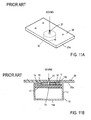
- Figs. 11A and 11B show a perspective view and sectional view of a configuration described in Japanese Patent Application Laid-Open No. 2005-192180 (hereinafter referred to as patent literature 1) as an example of a mounting structure for use to mount a microphone on a mounting board.
- reference numeral 10 denotes a microphone and 20 denotes a mounting board (board of a target equipment). Incidentally, internal structure of the microphone 10 is not shown in Fig. 11B.
- a sound hole 13 is formed in a circuit board 12 which covers an opening 11b of the capsule 11.
- External terminals 14 and 15 are formed on an external surface of the circuit board 12, and soldered to a terminal pattern (not shown) formed on the mounting board 20, thereby mounting the microphone 10 to the mounting board 20.
- Reference numeral 16 in Fig. 11B denotes a solder layer.
- a sound receiving through-hole (sound hole) 21 is formed in the mounting board 20, and the microphone 10 is mounted with the sound hole 13 in the circuit board 12 aligned with the through-hole 21 in the mounting board 20.
- the mounting board 20 can be placed in the equipment in such a way that a parts-mounting surface 20a will face inward in the equipment.
- a sound hole is formed in a front plate 11 a on the opposite side of the capsule 11 from the circuit board 12 rather than in the circuit board 12, it is necessary to place the mounting board 20 inside the equipment so that the parts-mounting surface 20a will face the sound source (turn outward) because the sound hole must face the sound source to capture the sound waves from the sound source. In that case, it is necessary to provide a space large enough to accommodate height of the microphone between the mounting board 20 and a housing of the equipment.
- the configuration shown in Figs. 11A and 11 B eliminates the need for such a space, and thus requires less space in order to mount the microphone.
- the sound hole 13 in the circuit board 12 of the microphone 10 and the through-hole 21 in the mounting board 20 are superimposed one upon the other; i.e., the sound hole 13 is placed at a location onto which the through-hole 21 is projected in a height direction of the microphone 10, making it easy for foreign matter such as dust and water droplets to get into the inner space of the microphone 10.
- any foreign matter entering the through-hole 21, for example, during an assembly process or the like may damage a diaphragm in the microphone.
- an object of the present invention is to provide a microphone and its mounting structure which are difficult for foreign matter to enter, capable of preventing a diaphragm from being damaged accidentally, and able to avoid pop noise, where the microphone is structured to capture sound waves through a sound receiving through-hole formed in a mounting board on which the microphone is surface-mounted.
- a microphone comprises a diaphragm, a back plate which faces the diaphragm at a distance therefrom to form a capacitor in conjunction therewith, a capsule which houses the diaphragm and the back plate, a circuit board which closes an opening of the capsule, and an external terminal installed on an external surface of the circuit board, the microphone being adapted to be mounted on a mounting board such that the external terminal is connected face to face with a connection terminal on the mounting board, wherein at least one sound receiving sound hole is formed in the circuit board without overlapping at least one sound receiving through-hole in the mounting board in a direction perpendicular to a board surface of the circuit board when the microphone is mounted; and the external terminal has a frame-like shape and surrounds the through-hole and the sound hole, forming an enclosed space via the face-to-face connection with the connection terminal, the enclosed space communicating the through-hole and the sound hole with each other.
- the external terminal may have a bump shape, protruding from the external surface of the circuit board.
- the bump shape may be formed of a thick-film conductor pattern or a conductive member on a conductor pattern.
- a stepped part protruding outward may be formed on the external surface of the circuit board, and the external terminal may be formed on the stepped part.
- a stepped plate which has steps may be installed in contact with the external surface; and the stepped plate may have a recess used to form the enclosed space, and a sound hole which opens to the recess, being communicated with the sound hole in the circuit board.
- a plurality of the sound holes may be arranged on a circle.
- a ground pattern may be formed in an area on the external surface of the circuit board, the area being surrounded by the external terminal.
- a microphone mounting structure for mounting a microphone on a mounting board, the microphone comprising a diaphragm, a back plate which faces the diaphragm at a distance therefrom to form a capacitor in conjunction therewith, a capsule which houses the diaphragm and the back plate, a circuit board which closes an opening of the capsule, and an external terminal installed on an external surface of the circuit board and connected face to face with a connection terminal on the mounting board, wherein at least one sound receiving sound hole is formed in the circuit board without overlapping at least one sound receiving through-hole in the mounting board when the microphone is mounted in a direction perpendicular to a board surface of the circuit board; and the external terminal has a frame-like shape and surrounds the through-hole and the sound hole, forming an enclosed space via the face-to-face connection with the connection terminal, the enclosed space communicating the through-hole and the sound hole with each other.
- one of the external terminal and the connection terminal may have a bump shape protruding toward the other.
- the bump shape may be formed of a thick-film conductor pattern or a conductive member on a conductor pattern.
- a plurality of the sound holes and a plurality of the through-holes may be arranged on concentric circles of different diameters inside the frame-like shape of the external terminal.
- a ground pattern may be formed, inside the frame-like shape of the external terminal, on each of opposing faces of the circuit board and the mounting board.
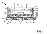
- Fig. 1 shows a configuration of an embodiment of the microphone according to the present invention with the microphone being mounted on a target mounting-board.
- the microphone 30 is an electret condenser microphone (ECM) in which an electret condenser is contained in a capsule 31 cylindrical in shape and a circuit board 32 circular in shape is housed in the capsule 31 in such as way as to close an opening 31c of the capsule 31 from inside.
- ECM electret condenser microphone
- the electret condenser includes a diaphragm 33, a back plate 34, and an electret (not shown) disposed on one surface of the back plate 34 which faces the diaphragm 33, the back plate 34 being disposed opposite a front plate 31a of the capsule 31.
- a washer ring 35 is interposed between the back plate 34 and front plate 31 a.
- the diaphragm 33 has its rim fixed to a support ring 36, and a ringshaped spacer 37 is interposed between the diaphragm 33 and back plate 34 to form a predetermined clearance.
- the support ring 36 is held on the circuit board 32 via a gate ring 38 mounted on the circuit board 32.
- an IC device 41 for impedance conversion is mounted on an internal surface of the circuit board, and external terminals 42 and 43 for external connection are formed on an external surface.
- the external terminals 42 and 43 have bump shapes which protrude from the external surface of the circuit board 32 farther than the crimp edges 31b of the capsule 31.
- the external terminals 42 and 43 are connected face to face to terminals on the mounting board 50.
- the connection is made by soldering using, for example, a reflow apparatus.
- reference numeral 51 denotes a solder layer.
- an enclosed space 52 is formed between the circuit board 32 and mounting board 50, communicating the sound holes 39 in the circuit board 32 with sound receiving through-holes 53 in the mounting board 50.
- the through-holes 53 in the mounting board 50 and sound holes 39 in the circuit board 32 are placed in such a position as to avoid overlapping each other in a direction perpendicular to a board surface of the mounting board 50. That is, the sound holes 39 are placed at locations other than locations onto which the through-holes 53 are projected in a height direction of the microphone 30.
- Fig. 2A is a sectional view showing a mounting structure of the microphone 30 in Fig. 1 in a simplified manner.
- Fig. 2B is a plan view of the mounting board 50 and
- Fig. 2C is a bottom view of the microphone 30.
- the external terminal 42 formed on the circuit board 32 of the microphone 30 is circular in shape and placed in the center of the circuit board 32 circular in shape.
- the other external terminal 43 which is shaped like a circular frame, concentrically surrounds the external terminal 42.
- the external terminals 42 and 43 are formed as a result of thin-film formation of a conductor pattern.
- such a thin-film conductor pattern can also be formed by plating or by print coating a conductive paste.
- the external terminal 42 is used as an output terminal while the external terminal 43 is used as a ground (GND) terminal.
- the sound holes 39 eight in number, are formed nearer to the external terminal 43 between the external terminals 42 and 43, and arranged at equal intervals concentrically with the external terminals 43 and 42.
- connection terminals 54 and 55 similar in shape to the external terminals 42 and 43 of the microphone 30, are created by pattern formation on the mounting board 50 at locations corresponding to the external terminals 42 and 43 as shown in Fig. 2B.
- the through-holes 53 are formed between the connection terminals 54 and 55.
- the through-holes 53 eight in number, are formed at equal intervals concentrically with the connection terminals 54 and 55. In this example, the through-holes 53 are formed nearer to the connection terminal 54 so that they will not overlap with the sound holes 39.
- connection terminals 54 and 55 are formed into such pattern shapes and connected face to face by soldering, a space surrounding the arrangements of the sound holes 39 and through-holes 53 is sealed by soldering, forming the enclosed space 52 between the circuit board 32 and mounting board 50.
- the microphone 30 configured as described above and mounted on the mounting board 50 allows sound waves from a sound source to be captured into inner space of the microphone 30 through the through-holes 53 of the mounting board 50, enclosed space 52, and sound holes 39 in the circuit board 32 of the microphone 30.
- the sound holes 39 in the circuit board 32 and through-holes 53 in the mounting board 50 are displaced from each other without overlap, making it difficult for foreign matter such as dust and water droplets to enter and preventing the diaphragm 33 from being damaged accidentally.
- the sound waves entering through the through-holes 53 are diffracted in the enclosed space 52, reach the sound holes 39, and then enter the microphone 30. That is, the diffraction structure in this example prevents the sound waves from directly reaching the diaphragm 33, and thereby makes it possible to reduce pop noise.
- the microphone 30 is mounted on the mounting board 50 by reflow soldering
- the external terminals 42 and 43 of the microphone 30 and connection terminals 54 and 55 of the mounting board 50 may be connected using, for example, a conductive adhesive instead of solder.
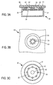
- Figs. 3A, 3B, and 3C show a configuration in which, out of the external terminals 42 and 43 formed on the circuit board 32 of the microphone 30 in Figs. 2A, 2B, and 2C, the pattern shape of the external terminal 43 serving as a ground terminal is changed in such a way that its inner rim juts in between adjacent sound holes 39 as shown in Fig. 3C. Such a pattern shape may also be used.
- the rest of the configuration is similar to that shown in Figs. 2A, 2B, and 2C.
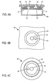
- Figs. 4A, 4B, and 4C which correspond to Figs. 2A, 2B, and 2C, show one through-hole 53 formed in the mounting board 50 and one sound hole 39 formed in the circuit board 32.
- the sound hole 39 and through-hole 53 are located 180 degrees apart from each other around a circular external terminal 42 and connection terminal 54 connected face to face with each other.
- the rest of the configuration is similar to that shown in Figs. 2A, 2B, and 2C.
- Figs. 4A, 4B, and 4C when mounting the microphone 30 on the mounting board 50, it is necessary to carry out positioning, making sure that there is no overlap between the sound hole 39 and through-hole 53.
- a possible method for the positioning involves putting marks on the capsule 31 of the microphone 30 and on the mounting board 50 in advance and aligning the marks to carry out positioning.
- Another method involves mounting the microphone 30 through image recognition using a camera.
- Figs. 5A, 5B, and 5C which correspond to Figs. 2A, 2B, and 2C, show another example of how to form a bump shape.
- the bump shape is formed by arranging and fixing conductive members on conductor patterns (thin-film conductor patterns) instead of using thick-film conductor patterns.
- reference characters 42a and 43a denote conductor patterns and 42b and 43b denote conductive members.
- Copper or brass may be used as a constituent material of the conductive members 42b and 43b.
- the external terminals 42 and 43 of a bump shape are produced as the conductive members 42b and 43b are soldered onto the conductor patterns 42a and 43a, respectively.
- the rest of the configuration is similar to that shown in Figs. 2A, 2B, and 2C.
- the external terminals 42 and 43 of the microphone 30 have a bump shape.
- the connection terminals 54 and 55 of the mounting board 50 may have a bump shape which is formed by using a thick-film conductor pattern or placing a conductive member on a conductor pattern.
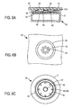
- This example involves placing a stepped plate 44 provided with steps in contact with the external surface of the circuit board 32 and creating external terminals 42' and 43' on top of the stepped plate 44 by pattern formation, instead of forming external terminals 42 and 43 of a bump shape on the circuit board 32 of the microphone 30.
- a recess 45 annular in shape is formed on the stepped plate 44 except where the external terminals 42' and 43' are formed.
- an enclosed space 52 is formed between the circuit board 32 and mounting board 50.
- Sound holes 46 which open to the recess 45 are formed in the stepped plate 44 in communication with the sound holes 39 in the circuit board 32.
- the stepped plate 44 and circuit board 32 are integrated by joining conductor patterns formed on their opposing faces using solder or a conductive adhesive.
- the conductor patterns formed on that surface of the stepped plate 44 which opposes the circuit board 32 are connected with the external terminals 42' and 43' via through-holes or the like.
- stepped plate 44 (shown in Fig. 6) which has steps makes it possible to easily set the external terminals 42' and 43' to desired height positions, i.e., desired positions higher than the crimp edges 31b of the capsule 31, and form the enclosed space 52.
- stepped plate 44 is joined integrally to the circuit board 32 of the microphone 30, stepped parts extruding outward may be formed on the circuit board 32 itself and then patterns of the external terminals 42' and 43' may be formed on the steps.
- one sound hole 39 and one through-hole 53 are formed in the circuit board 32 and mounting board 50, respectively, as in the case of the configuration shown in Fig. 4.
- annular ground patterns 47 and 56 are formed in the area between the external terminals 42 and 43 and the area between the connection terminals 54 and 55, respectively, on the opposing faces of the circuit board 32 and mounting board 50, with a clearance provided between the output terminal 42 and ground pattern 47 as well as between output terminal 54 and ground pattern 56.
- the ground patterns 47 and 56 which are formed in this way on the surfaces facing the sound hole 39 and through-hole 53 make it possible to shield out electromagnetic waves entering directly and thereby suppress induction noise.
- the shielding effect of the ground patterns 47 and 56 is enhanced by the displacement between the sound hole 39 and through-hole 53.
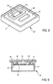
- Fig. 8 shows a microphone whose external shape is square/rectangular rather than cylindrical which is the case with the above examples.
- An external terminal 48 rectangular in shape and external terminal 49 square in shape are formed next to each other on a circuit board 32' which closes an opening of a capsule 31'.
- the external terminals 48 and 49 have a bump shape.
- the external terminal 48 is an output terminal and the external terminal 49 is a ground terminal.
- Two sound holes 39 are formed within a frame of the external terminal 49 on the circuit board 32'.
- Fig. 9 is a simplified view of the microphone 30' in Fig. 8 as the microphone 30' is mounted on the mounting board 50.
- Figs. 10A and 10B are a plan view of the mounting board 50 and a bottom view of the microphone 30', respectively.
- connection terminals 57 and 58 are formed on the mounting board 50, corresponding to the external terminals 48 and 49.
- One through-hole 53 is formed in the center of a frame of the terminal 58.
- the through-hole 53 in the mounting board 50 and sound hole 39 in the circuit board 32' are located in such positions that there will be no overlap between the holes as shown in Fig. 9.
- An enclosed space 52 is formed between the mounting board 50 and circuit board 32' and the through-hole 53 and sound hole 39 are communicated with each other via the enclosed space 52.
- a microphone is configured such that a sound hole formed in a circuit board does not overlap a sound receiving through-hole formed in a mounting board on which the microphone is mounted; therefore, it is possible to reduce foreign matter to enter the microphone, prevent a diaphragm from being damaged accidentally, and reduce pop noise.
Landscapes
- Engineering & Computer Science (AREA)
- Physics & Mathematics (AREA)
- Acoustics & Sound (AREA)
- Signal Processing (AREA)
- Microelectronics & Electronic Packaging (AREA)
- Electrostatic, Electromagnetic, Magneto- Strictive, And Variable-Resistance Transducers (AREA)
- Details Of Audible-Bandwidth Transducers (AREA)
Abstract
Description
- The present invention relates to a microphone and a microphone mounting structure incorporated, for example, in a cell phone.
- Downsizing, ease of mounting, and reduced requirements for mounting space are demanded of microphones to be mounted in such small equipment as cell phones.
- Electret condenser microphones (ECM) are commonly used as such microphones that are provided with good characteristics, easy to handle because of their simple structure, and easy to downsize. They are mounted on a target mounting-board (board of a target equipment) using a surface-mount technique.
- Figs. 11A and 11B show a perspective view and sectional view of a configuration described in
Japanese Patent Application Laid-Open No. 2005-192180 reference numeral 10 denotes a microphone and 20 denotes a mounting board (board of a target equipment). Incidentally, internal structure of themicrophone 10 is not shown in Fig. 11B. - In this example, as shown in Fig. 11B, no sound receiving sound hole is formed in a
capsule 11 which provides a shell of themicrophone 10, but asound hole 13 is formed in acircuit board 12 which covers an opening 11b of thecapsule 11.External terminals circuit board 12, and soldered to a terminal pattern (not shown) formed on themounting board 20, thereby mounting themicrophone 10 to themounting board 20.Reference numeral 16 in Fig. 11B denotes a solder layer. - A sound receiving through-hole (sound hole) 21 is formed in the
mounting board 20, and themicrophone 10 is mounted with thesound hole 13 in thecircuit board 12 aligned with the through-hole 21 in themounting board 20. - With the mounting structure in this example, sound waves from a sound source are captured into inner space of the
microphone 10 through the through-hole 21 in themounting board 20 and thesound hole 13 in thecircuit board 12. Thus, in this example, themounting board 20 can be placed in the equipment in such a way that a parts-mountingsurface 20a will face inward in the equipment. - That is, if a sound hole is formed in a
front plate 11 a on the opposite side of thecapsule 11 from thecircuit board 12 rather than in thecircuit board 12, it is necessary to place themounting board 20 inside the equipment so that the parts-mounting surface 20a will face the sound source (turn outward) because the sound hole must face the sound source to capture the sound waves from the sound source. In that case, it is necessary to provide a space large enough to accommodate height of the microphone between themounting board 20 and a housing of the equipment. However, the configuration shown in Figs. 11A and 11 B eliminates the need for such a space, and thus requires less space in order to mount the microphone. - However, with the conventional mounting structure shown in Figs. 11 A and 11B, the
sound hole 13 in thecircuit board 12 of themicrophone 10 and the through-hole 21 in themounting board 20 are superimposed one upon the other; i.e., thesound hole 13 is placed at a location onto which the through-hole 21 is projected in a height direction of themicrophone 10, making it easy for foreign matter such as dust and water droplets to get into the inner space of themicrophone 10. - Also, since the positions of the
sound hole 13 and through-hole 21 coincide, any foreign matter entering the through-hole 21, for example, during an assembly process or the like may damage a diaphragm in the microphone. - Furthermore, the sound waves, which enter the diaphragm directly through the through-
hole 21 and thesound hole 13, are liable to cause pop noise. - In view of the above problems, an object of the present invention is to provide a microphone and its mounting structure which are difficult for foreign matter to enter, capable of preventing a diaphragm from being damaged accidentally, and able to avoid pop noise, where the microphone is structured to capture sound waves through a sound receiving through-hole formed in a mounting board on which the microphone is surface-mounted.
- According to a first aspect of the present invention, a microphone comprises a diaphragm, a back plate which faces the diaphragm at a distance therefrom to form a capacitor in conjunction therewith, a capsule which houses the diaphragm and the back plate, a circuit board which closes an opening of the capsule, and an external terminal installed on an external surface of the circuit board, the microphone being adapted to be mounted on a mounting board such that the external terminal is connected face to face with a connection terminal on the mounting board,
wherein at least one sound receiving sound hole is formed in the circuit board without overlapping at least one sound receiving through-hole in the mounting board in a direction perpendicular to a board surface of the circuit board when the microphone is mounted; and
the external terminal has a frame-like shape and surrounds the through-hole and the sound hole, forming an enclosed space via the face-to-face connection with the connection terminal, the enclosed space communicating the through-hole and the sound hole with each other. - In the microphone, the external terminal may have a bump shape, protruding from the external surface of the circuit board.
- The bump shape may be formed of a thick-film conductor pattern or a conductive member on a conductor pattern.
- In the microphone, a stepped part protruding outward may be formed on the external surface of the circuit board, and the external terminal may be formed on the stepped part.
- In the microphone, a stepped plate which has steps may be installed in contact with the external surface; and the stepped plate may have a recess used to form the enclosed space, and a sound hole which opens to the recess, being communicated with the sound hole in the circuit board.
- In the microphone, a plurality of the sound holes may be arranged on a circle.
- In the microphone, a ground pattern may be formed in an area on the external surface of the circuit board, the area being surrounded by the external terminal.
- According to a second aspect of the present invention, a microphone mounting structure for mounting a microphone on a mounting board, the microphone comprising a diaphragm, a back plate which faces the diaphragm at a distance therefrom to form a capacitor in conjunction therewith, a capsule which houses the diaphragm and the back plate, a circuit board which closes an opening of the capsule, and an external terminal installed on an external surface of the circuit board and connected face to face with a connection terminal on the mounting board,
wherein at least one sound receiving sound hole is formed in the circuit board without overlapping at least one sound receiving through-hole in the mounting board when the microphone is mounted in a direction perpendicular to a board surface of the circuit board; and
the external terminal has a frame-like shape and surrounds the through-hole and the sound hole, forming an enclosed space via the face-to-face connection with the connection terminal, the enclosed space communicating the through-hole and the sound hole with each other. - In the mounting structure, one of the external terminal and the connection terminal may have a bump shape protruding toward the other.
- The bump shape may be formed of a thick-film conductor pattern or a conductive member on a conductor pattern.
- In the mounting structure, a plurality of the sound holes and a plurality of the through-holes may be arranged on concentric circles of different diameters inside the frame-like shape of the external terminal.
- In the mounting structure, a ground pattern may be formed, inside the frame-like shape of the external terminal, on each of opposing faces of the circuit board and the mounting board.
-
- Fig. 1 is a sectional view illustrating a first embodiment of the present invention;
- Fig. 2A is a simplified version of the sectional view in Fig. 1, shown upside down;
- Fig. 2B is a plan view of a mounting board in Fig. 1;
- Fig. 2C is a bottom view of a microphone in Fig. 1;
- Fig. 3A is a sectional view of a second embodiment of the microphone according to the present invention;
- Fig. 3B is a plan view of a mounting board;
- Fig. 3C is a bottom view of the microphone;
- Fig. 4A is a sectional view of a third embodiment of the microphone according to the present invention;
- Fig. 4B is a plan view of a mounting board;
- Fig. 4C is a bottom view of the microphone;
- Fig. 5A is a sectional view of a fourth embodiment of the microphone according to the present invention;
- Fig. 5B is a plan view of a mounting board;
- Fig. 5C is a bottom view of the microphone;
- Fig. 6A is a sectional view of a fifth embodiment of the microphone according to the present invention;
- Fig. 6B is a plan view of a mounting board;
- Fig. 6C is a bottom view of the microphone;
- Fig. 7 is a sectional view illustrating a sixth embodiment of the present invention;
- Fig. 8 is a perspective view illustrating a seventh embodiment of the present invention;
- Fig. 9 is a sectional view showing a mounted state of a microphone shown in Fig. 8;
- Fig. 10A is a plan view of a mounting board in Fig. 9;
- Fig. 10B is a bottom view of the microphone in Fig. 9;
- Fig. 11A is a perspective view showing a prior art example of a mounting structure for mounting a microphone on a mounting board; and
- Fig. 11B is a sectional view.
- Embodiments of the present invention will be described with reference to the drawings.
- Fig. 1 shows a configuration of an embodiment of the microphone according to the present invention with the microphone being mounted on a target mounting-board.
- In this example, the
microphone 30 is an electret condenser microphone (ECM) in which an electret condenser is contained in acapsule 31 cylindrical in shape and acircuit board 32 circular in shape is housed in thecapsule 31 in such as way as to close anopening 31c of thecapsule 31 from inside. - The electret condenser includes a
diaphragm 33, aback plate 34, and an electret (not shown) disposed on one surface of theback plate 34 which faces thediaphragm 33, theback plate 34 being disposed opposite afront plate 31a of thecapsule 31. Awasher ring 35 is interposed between theback plate 34 andfront plate 31 a. - The
diaphragm 33 has its rim fixed to asupport ring 36, and aringshaped spacer 37 is interposed between thediaphragm 33 and backplate 34 to form a predetermined clearance. Thesupport ring 36 is held on thecircuit board 32 via agate ring 38 mounted on thecircuit board 32. - To fix the
circuit board 32, open ends of thecapsule 31 is bent inward by crimping and thecircuit board 32 is fixed under pressure by resulting crimp edges 31b. - Multiple sound holes 39 are formed in the
circuit board 32, anIC device 41 for impedance conversion is mounted on an internal surface of the circuit board, andexternal terminals external terminals circuit board 32 farther than the crimp edges 31b of thecapsule 31. - To mount the
microphone 30 on a mountingboard 50, theexternal terminals board 50. The connection is made by soldering using, for example, a reflow apparatus. In Fig. 1,reference numeral 51 denotes a solder layer. - As the
external terminals microphone 30 are connected to the terminals on the mountingboard 50 by soldering in this way, anenclosed space 52 is formed between thecircuit board 32 and mountingboard 50, communicating the sound holes 39 in thecircuit board 32 with sound receiving through-holes 53 in the mountingboard 50. Incidentally, the through-holes 53 in the mountingboard 50 andsound holes 39 in thecircuit board 32 are placed in such a position as to avoid overlapping each other in a direction perpendicular to a board surface of the mountingboard 50. That is, the sound holes 39 are placed at locations other than locations onto which the through-holes 53 are projected in a height direction of themicrophone 30. - Fig. 2A is a sectional view showing a mounting structure of the
microphone 30 in Fig. 1 in a simplified manner. Fig. 2B is a plan view of the mountingboard 50 and Fig. 2C is a bottom view of themicrophone 30. As shown in Fig. 2C, theexternal terminal 42 formed on thecircuit board 32 of themicrophone 30 is circular in shape and placed in the center of thecircuit board 32 circular in shape. The otherexternal terminal 43, which is shaped like a circular frame, concentrically surrounds theexternal terminal 42. In this example, theexternal terminals - The
external terminal 42 is used as an output terminal while theexternal terminal 43 is used as a ground (GND) terminal. In this example, the sound holes 39, eight in number, are formed nearer to theexternal terminal 43 between theexternal terminals external terminals - On the other hand,
connection terminals external terminals microphone 30, are created by pattern formation on the mountingboard 50 at locations corresponding to theexternal terminals holes 53 are formed between theconnection terminals holes 53, eight in number, are formed at equal intervals concentrically with theconnection terminals holes 53 are formed nearer to theconnection terminal 54 so that they will not overlap with the sound holes 39. - As the
external terminals connection terminals holes 53 is sealed by soldering, forming theenclosed space 52 between thecircuit board 32 and mountingboard 50. - In this example, the
microphone 30 configured as described above and mounted on the mountingboard 50 allows sound waves from a sound source to be captured into inner space of themicrophone 30 through the through-holes 53 of the mountingboard 50, enclosedspace 52, andsound holes 39 in thecircuit board 32 of themicrophone 30. - In this example, unlike the mounting structure shown in Fig. 11, the sound holes 39 in the
circuit board 32 and through-holes 53 in the mountingboard 50 are displaced from each other without overlap, making it difficult for foreign matter such as dust and water droplets to enter and preventing thediaphragm 33 from being damaged accidentally. In addition, the sound waves entering through the through-holes 53 are diffracted in the enclosedspace 52, reach the sound holes 39, and then enter themicrophone 30. That is, the diffraction structure in this example prevents the sound waves from directly reaching thediaphragm 33, and thereby makes it possible to reduce pop noise. - Incidentally, although in the above example, the
microphone 30 is mounted on the mountingboard 50 by reflow soldering, theexternal terminals microphone 30 andconnection terminals board 50 may be connected using, for example, a conductive adhesive instead of solder. - Figs. 3A, 3B, and 3C show a configuration in which, out of the
external terminals circuit board 32 of themicrophone 30 in Figs. 2A, 2B, and 2C, the pattern shape of theexternal terminal 43 serving as a ground terminal is changed in such a way that its inner rim juts in between adjacentsound holes 39 as shown in Fig. 3C. Such a pattern shape may also be used. The rest of the configuration is similar to that shown in Figs. 2A, 2B, and 2C. - Although in the examples shown in Figs. 2A, 2B, and 2C and Figs. 3A, 3B, and 3C, eight
sound holes 39 and eight through-holes 53 are arranged on circles, the numbers of the sound holes 39 and through-holes 53 may be set as required including one. - Figs. 4A, 4B, and 4C, which correspond to Figs. 2A, 2B, and 2C, show one through-
hole 53 formed in the mountingboard 50 and onesound hole 39 formed in thecircuit board 32. In this example, to avoid overlap, thesound hole 39 and through-hole 53 are located 180 degrees apart from each other around a circularexternal terminal 42 andconnection terminal 54 connected face to face with each other. The rest of the configuration is similar to that shown in Figs. 2A, 2B, and 2C. - With the configuration shown in Figs. 4A, 4B, and 4C, when mounting the
microphone 30 on the mountingboard 50, it is necessary to carry out positioning, making sure that there is no overlap between thesound hole 39 and through-hole 53. A possible method for the positioning involves putting marks on thecapsule 31 of themicrophone 30 and on the mountingboard 50 in advance and aligning the marks to carry out positioning. Another method involves mounting themicrophone 30 through image recognition using a camera. - Figs. 5A, 5B, and 5C, which correspond to Figs. 2A, 2B, and 2C, show another example of how to form a bump shape. In this example, the bump shape is formed by arranging and fixing conductive members on conductor patterns (thin-film conductor patterns) instead of using thick-film conductor patterns. In Fig. 5A,
reference characters - Copper or brass, for example, may be used as a constituent material of the
conductive members external terminals conductive members conductor patterns - In all the examples described above, the
external terminals microphone 30 have a bump shape. Alternatively, theconnection terminals board 50 may have a bump shape which is formed by using a thick-film conductor pattern or placing a conductive member on a conductor pattern. By giving a bump shape to theexternal terminals connection terminals enclosed space 52 between the mountingboard 50 and thecircuit board 32 of themicrophone 30. When themicrophone 30 is mounted on the mountingboard 50 by reflow soldering, by giving a bump shape to theexternal terminals microphone 30, it is possible to prevent solder from entering (flowing around into) themicrophone 30. - Next, an embodiment shown in Figs. 6A, 6B, and 6C will be described.
- This example involves placing a stepped
plate 44 provided with steps in contact with the external surface of thecircuit board 32 and creating external terminals 42' and 43' on top of the steppedplate 44 by pattern formation, instead of formingexternal terminals circuit board 32 of themicrophone 30. Arecess 45 annular in shape is formed on the steppedplate 44 except where the external terminals 42' and 43' are formed. As the steppedplate 44 with therecess 45 is placed on the external surface of thecircuit board 32, anenclosed space 52 is formed between thecircuit board 32 and mountingboard 50. - Sound holes 46 which open to the
recess 45 are formed in the steppedplate 44 in communication with the sound holes 39 in thecircuit board 32. Incidentally, the steppedplate 44 andcircuit board 32 are integrated by joining conductor patterns formed on their opposing faces using solder or a conductive adhesive. The conductor patterns formed on that surface of the steppedplate 44 which opposes thecircuit board 32 are connected with the external terminals 42' and 43' via through-holes or the like. - The use of the stepped plate 44 (shown in Fig. 6) which has steps makes it possible to easily set the external terminals 42' and 43' to desired height positions, i.e., desired positions higher than the crimp edges 31b of the
capsule 31, and form the enclosedspace 52. - Incidentally, although in Fig. 6, the stepped
plate 44 is joined integrally to thecircuit board 32 of themicrophone 30, stepped parts extruding outward may be formed on thecircuit board 32 itself and then patterns of the external terminals 42' and 43' may be formed on the steps. - Next, an embodiment shown in Fig. 7 will be described.
- In this example, one
sound hole 39 and one through-hole 53 are formed in thecircuit board 32 and mountingboard 50, respectively, as in the case of the configuration shown in Fig. 4. Besides,annular ground patterns external terminals connection terminals circuit board 32 and mountingboard 50, with a clearance provided between theoutput terminal 42 andground pattern 47 as well as betweenoutput terminal 54 andground pattern 56. - The
ground patterns sound hole 39 and through-hole 53 make it possible to shield out electromagnetic waves entering directly and thereby suppress induction noise. Incidentally, the shielding effect of theground patterns sound hole 39 and through-hole 53. With the conventional mounting structure shown in Fig. 11 in which thesound hole 13 in thecircuit board 12 of themicrophone 10 coincides in position with the through-hole 21 in the mounting board 20 (i.e., they are superimposed one upon the other), sufficient shielding effect is not available, i.e., electromagnetic waves enter the inner space of the microphone even if such ground patterns are installed. - Fig. 8 shows a microphone whose external shape is square/rectangular rather than cylindrical which is the case with the above examples. An
external terminal 48 rectangular in shape and external terminal 49 square in shape are formed next to each other on a circuit board 32' which closes an opening of a capsule 31'. Theexternal terminals - In this example, the
external terminal 48 is an output terminal and theexternal terminal 49 is a ground terminal. Twosound holes 39 are formed within a frame of theexternal terminal 49 on the circuit board 32'. - Fig. 9 is a simplified view of the microphone 30' in Fig. 8 as the microphone 30' is mounted on the mounting
board 50. Figs. 10A and 10B are a plan view of the mountingboard 50 and a bottom view of the microphone 30', respectively. - Patterns of
connection terminals board 50, corresponding to theexternal terminals hole 53 is formed in the center of a frame of the terminal 58. - When the microphone 30' is mounted on the mounting
board 50, the through-hole 53 in the mountingboard 50 andsound hole 39 in the circuit board 32' are located in such positions that there will be no overlap between the holes as shown in Fig. 9. Anenclosed space 52 is formed between the mountingboard 50 and circuit board 32' and the through-hole 53 andsound hole 39 are communicated with each other via the enclosedspace 52. - According to the present invention, a microphone is configured such that a sound hole formed in a circuit board does not overlap a sound receiving through-hole formed in a mounting board on which the microphone is mounted; therefore, it is possible to reduce foreign matter to enter the microphone, prevent a diaphragm from being damaged accidentally, and reduce pop noise.
Claims (14)
- A microphone comprising a diaphragm, a back plate which faces the diaphragm at a distance therefrom to form a capacitor in conjunction therewith, a capsule which houses the diaphragm and the back plate, a circuit board which closes an opening of the capsule, and an external terminal installed on an external surface of the circuit board, the microphone being adapted to be mounted on a mounting board such that the external terminal is connected face to face with a connection terminal on the mounting board,
wherein at least one sound receiving sound hole is formed in the circuit board without overlapping at least one sound receiving through-hole in the mounting board in a direction perpendicular to a board surface of the circuit board when the microphone is mounted; and
the external terminal has a frame-like shape and surrounds the through-hole and the sound hole, forming an enclosed space via the face-to-face connection with the connection terminal, the enclosed space communicating the through-hole and the sound hole with each other. - The microphone according to Claim 1, wherein the external terminal has a bump shape, protruding from the external surface of the circuit board and surrounding the through-hole and the sound hole in a plane parallel to the external surface of the circuit board.
- The microphone according to Claim 2, wherein the bump shape is formed of a thick-film conductor pattern.
- The microphone according to Claim 2, wherein the bump shape is formed of a conductive member on a conductor pattern.
- The microphone according to Claim 1, wherein a stepped part protruding outward is formed on the external surface of the circuit board; and the external terminal is formed on the stepped part.
- The microphone according to Claim 1, wherein the external terminal is formed on a stepped plate installed in contact with the external surface of said circuit board and provided with steps; the stepped plate has a recess used to form the enclosed space, and a sound hole which opens to the recess, being communicated with the sound hole in the circuit board.
- The microphone according to Claim 1, wherein a plurality of the sound holes are formed on a circle inside the frame-like shape of the external terminal.
- The microphone according to Claim 1, wherein when the microphone is mounted, ground patterns are formed, inside the external terminal, on opposing faces of the circuit board and the mounting board.
- A microphone mounting structure for mounting a microphone on a mounting board, the microphone comprising a diaphragm, a back plate which faces the diaphragm at a distance therefrom to form a capacitor in conjunction therewith, a capsule which houses the diaphragm and the back plate, a circuit board which closes an opening of the capsule, and an external terminal installed on an external surface of the circuit board and connected face to face with a connection terminal on the mounting board,
wherein at least one sound receiving sound hole is formed in the circuit board without overlapping at least one sound receiving through-hole in the mounting board when the microphone is mounted in a direction perpendicular to a board surface of the circuit board; and
the external terminal has a frame-like shape and surrounds the through-hole and the sound hole, forming an enclosed space via the face-to-face connection with the connection terminal, the enclosed space communicating the through-hole and the sound hole with each other. - The microphone mounting structure according to Claim 9, wherein one of the external terminal and the connection terminal has a bump shape protruding toward the other.
- The microphone mounting structure according to Claim 10, wherein the bump shape is formed of a thick-film conductor pattern.
- The microphone mounting structure according to Claim 10, wherein the bump shape is formed of a conductive member on a conductor pattern.
- The microphone mounting structure according to Claim 9, wherein a plurality of the sound holes and a plurality of the through-holes are arranged on concentric circles of different diameters inside the frame-like shape of the external terminal.
- The microphone mounting structure according to Claim 9, wherein ground patterns are formed, inside the frame-like shape of the external terminal, on opposing faces of the circuit board and the mounting board.
Applications Claiming Priority (1)
| Application Number | Priority Date | Filing Date | Title |
|---|---|---|---|
| JP2006305101A JP4328347B2 (en) | 2006-11-10 | 2006-11-10 | Microphone and its mounting structure |
Publications (3)
| Publication Number | Publication Date |
|---|---|
| EP1921891A2 true EP1921891A2 (en) | 2008-05-14 |
| EP1921891A3 EP1921891A3 (en) | 2009-03-04 |
| EP1921891B1 EP1921891B1 (en) | 2010-05-12 |
Family
ID=39032179
Family Applications (1)
| Application Number | Title | Priority Date | Filing Date |
|---|---|---|---|
| EP07021596A Not-in-force EP1921891B1 (en) | 2006-11-10 | 2007-11-07 | Microphone and mounted microphone structure |
Country Status (7)
| Country | Link |
|---|---|
| US (1) | US8050443B2 (en) |
| EP (1) | EP1921891B1 (en) |
| JP (1) | JP4328347B2 (en) |
| KR (1) | KR100935062B1 (en) |
| CN (1) | CN101247675B (en) |
| DE (1) | DE602007006394D1 (en) |
| TW (1) | TW200829058A (en) |
Cited By (4)
| Publication number | Priority date | Publication date | Assignee | Title |
|---|---|---|---|---|
| WO2012094722A1 (en) | 2011-01-12 | 2012-07-19 | Research In Motion Limited | Printed circuit board with an acoustic channel for a microphone |
| WO2013045749A1 (en) * | 2011-09-29 | 2013-04-04 | Nokia Corporation | Dust protection of sound transducer |
| EP2584793A3 (en) * | 2011-10-18 | 2014-05-21 | Hosiden Corporation | Electret condenser microphone |
| CN105917669A (en) * | 2014-12-25 | 2016-08-31 | 华为技术有限公司 | Microphone |
Families Citing this family (17)
| Publication number | Priority date | Publication date | Assignee | Title |
|---|---|---|---|---|
| RU2401341C1 (en) * | 2006-07-25 | 2010-10-10 | ЭлДжи ЭЛЕКТРОНИКС ИНК. | Additional machine for treatment of linen and multifunctional machine for treatment of linen, comprising such additional machine |
| KR100982239B1 (en) * | 2007-11-02 | 2010-09-14 | 주식회사 비에스이 | MEMS microphone package with sound hole in PCB |
| JP5183340B2 (en) * | 2008-07-23 | 2013-04-17 | 日本電波工業株式会社 | Surface mount type oscillator and electronic device equipped with this oscillator |
| JP4809912B2 (en) * | 2009-07-03 | 2011-11-09 | ホシデン株式会社 | Condenser microphone |
| PL2312290T3 (en) * | 2009-10-16 | 2020-06-01 | First Sensor Mobility Gmbh | Pressure sensor and use of same in a fluid tank |
| US9544678B2 (en) * | 2011-01-12 | 2017-01-10 | Blackberry Limited | Printed circuit board with an acoustic channel for a microphone |
| KR101293056B1 (en) * | 2011-12-05 | 2013-08-05 | 주식회사 비에스이 | Microphone assembly having ear set function and method of making the same |
| US8965027B2 (en) * | 2013-02-15 | 2015-02-24 | Invensense, Inc. | Packaged microphone with frame having die mounting concavity |
| JP6245249B2 (en) * | 2013-02-22 | 2017-12-13 | パナソニック株式会社 | Electronic component package |
| US9439017B2 (en) * | 2014-02-10 | 2016-09-06 | Infineon Technologies Ag | Method for manufacturing a plurality of microphone structures, microphone and mobile device |
| GB2526846B (en) | 2014-06-05 | 2020-03-25 | Nokia Technologies Oy | An apparatus and method for providing an apparatus comprising an audio transducer |
| US9226081B1 (en) * | 2014-11-21 | 2015-12-29 | Zilltek Technology (Shanghai) Corp. | Digital electret microphone and the connection structure thereof |
| KR101593926B1 (en) | 2015-04-29 | 2016-02-16 | 싸니코전자 주식회사 | Microphone mounted structure of mainboard with multimedia device |
| KR102148245B1 (en) * | 2017-12-01 | 2020-08-26 | 주식회사 더하일 | Text to speech system |
| KR102330345B1 (en) * | 2019-02-12 | 2021-11-23 | 주식회사 더하일 | CTS conbine system with PU |
| CN218679381U (en) * | 2020-06-30 | 2023-03-21 | 瑞声声学科技(深圳)有限公司 | Vibration sensor |
| EP4496344A4 (en) * | 2023-05-30 | 2026-04-15 | Samsung Electronics Co Ltd | ELECTRONIC DEVICE WITH AUDIO INPUT DEVICE |
Citations (3)
| Publication number | Priority date | Publication date | Assignee | Title |
|---|---|---|---|---|
| EP1427250A2 (en) | 2002-12-03 | 2004-06-09 | Hosiden Corporation | Electret microphone |
| EP1494503A1 (en) | 2002-04-05 | 2005-01-05 | Matsushita Electric Industrial Co., Ltd. | Capacitor sensor |
| EP1530401A2 (en) | 2003-11-05 | 2005-05-11 | BSE Co., Ltd. | Method of mounting condenser microphone on main PCB and condenser microphone adapted for the same |
Family Cites Families (5)
| Publication number | Priority date | Publication date | Assignee | Title |
|---|---|---|---|---|
| JPS6017191B2 (en) | 1977-12-30 | 1985-05-01 | アイホン株式会社 | Microphone unit with wind noise attenuation effect |
| JP3593554B2 (en) | 1995-05-26 | 2004-11-24 | フオスター電機株式会社 | Wind noise prevention microphone |
| KR100603139B1 (en) | 2004-03-18 | 2006-07-20 | 주식회사 비에스이 | Directional electret condenser microphone |
| JP2006238203A (en) | 2005-02-25 | 2006-09-07 | Hosiden Corp | Microphone |
| JP4150407B2 (en) | 2005-06-20 | 2008-09-17 | ホシデン株式会社 | Electroacoustic transducer |
-
2006
- 2006-11-10 JP JP2006305101A patent/JP4328347B2/en active Active
-
2007
- 2007-10-23 TW TW096139687A patent/TW200829058A/en not_active IP Right Cessation
- 2007-11-01 US US11/982,501 patent/US8050443B2/en active Active
- 2007-11-07 DE DE602007006394T patent/DE602007006394D1/en active Active
- 2007-11-07 KR KR1020070113081A patent/KR100935062B1/en not_active Expired - Fee Related
- 2007-11-07 EP EP07021596A patent/EP1921891B1/en not_active Not-in-force
- 2007-11-12 CN CN2007103035835A patent/CN101247675B/en active Active
Patent Citations (3)
| Publication number | Priority date | Publication date | Assignee | Title |
|---|---|---|---|---|
| EP1494503A1 (en) | 2002-04-05 | 2005-01-05 | Matsushita Electric Industrial Co., Ltd. | Capacitor sensor |
| EP1427250A2 (en) | 2002-12-03 | 2004-06-09 | Hosiden Corporation | Electret microphone |
| EP1530401A2 (en) | 2003-11-05 | 2005-05-11 | BSE Co., Ltd. | Method of mounting condenser microphone on main PCB and condenser microphone adapted for the same |
Cited By (9)
| Publication number | Priority date | Publication date | Assignee | Title |
|---|---|---|---|---|
| WO2012094722A1 (en) | 2011-01-12 | 2012-07-19 | Research In Motion Limited | Printed circuit board with an acoustic channel for a microphone |
| EP2664221A4 (en) * | 2011-01-12 | 2017-03-29 | BlackBerry Limited | Printed circuit board with an acoustic channel for a microphone |
| WO2013045749A1 (en) * | 2011-09-29 | 2013-04-04 | Nokia Corporation | Dust protection of sound transducer |
| US8644530B2 (en) | 2011-09-29 | 2014-02-04 | Nokia Corporation | Dust protection of sound transducer |
| US9473838B2 (en) | 2011-09-29 | 2016-10-18 | Nokia Technologies Oy | Dust protection of sound transducer |
| EP2584793A3 (en) * | 2011-10-18 | 2014-05-21 | Hosiden Corporation | Electret condenser microphone |
| CN105917669A (en) * | 2014-12-25 | 2016-08-31 | 华为技术有限公司 | Microphone |
| EP3229492A4 (en) * | 2014-12-25 | 2017-12-06 | Huawei Technologies Co., Ltd. | Microphone |
| CN105917669B (en) * | 2014-12-25 | 2019-12-24 | 华为技术有限公司 | microphone |
Also Published As
| Publication number | Publication date |
|---|---|
| TW200829058A (en) | 2008-07-01 |
| US20080112585A1 (en) | 2008-05-15 |
| EP1921891B1 (en) | 2010-05-12 |
| KR100935062B1 (en) | 2009-12-31 |
| KR20080042703A (en) | 2008-05-15 |
| CN101247675B (en) | 2012-05-23 |
| JP4328347B2 (en) | 2009-09-09 |
| JP2008124698A (en) | 2008-05-29 |
| TWI376963B (en) | 2012-11-11 |
| EP1921891A3 (en) | 2009-03-04 |
| DE602007006394D1 (en) | 2010-06-24 |
| CN101247675A (en) | 2008-08-20 |
| US8050443B2 (en) | 2011-11-01 |
Similar Documents
| Publication | Publication Date | Title |
|---|---|---|
| US8050443B2 (en) | Microphone and microphone mounting structure | |
| KR100673849B1 (en) | Condenser microphone mounted on main board and mobile communication terminal including the same | |
| EP2352311B1 (en) | Microphone | |
| US8126166B2 (en) | Condenser microphone and packaging method for the same | |
| JP2007081614A (en) | Condenser microphone | |
| JP4777406B2 (en) | MEMS microphone package | |
| JP3908059B2 (en) | Electret condenser microphone | |
| US20090092274A1 (en) | Silicon condenser microphone having additional back chamber and sound hole in pcb | |
| JP2008187607A (en) | Semiconductor device | |
| KR100664357B1 (en) | Electro acoustic conversion device having rear terminal | |
| EP1109422A2 (en) | Condenser microphone | |
| JP2003153392A (en) | Electret capacitor microphone | |
| JP2006165201A (en) | Circuit module device | |
| US7558077B2 (en) | Electronic device | |
| EP1699258B1 (en) | Electro-acoustic transducer with holder | |
| KR100507547B1 (en) | Communication apparatus and method of fabricating the same | |
| JP3748810B2 (en) | Microphone | |
| JP2006174426A (en) | Condenser microphone and method of manufacturing substrate thereof | |
| JP2006157837A (en) | Capacitor microphone | |
| CN216905295U (en) | Microphone structure and electronic equipment | |
| JPH07142906A (en) | Dielectric filter lid mounting structure | |
| US8130506B2 (en) | Sensor module | |
| JPH09321481A (en) | Light receiving device | |
| KR101731041B1 (en) | Microphone package | |
| EP2009952A2 (en) | Condenser microphone |
Legal Events
| Date | Code | Title | Description |
|---|---|---|---|
| PUAI | Public reference made under article 153(3) epc to a published international application that has entered the european phase |
Free format text: ORIGINAL CODE: 0009012 |
|
| 17P | Request for examination filed |
Effective date: 20071107 |
|
| AK | Designated contracting states |
Kind code of ref document: A2 Designated state(s): AT BE BG CH CY CZ DE DK EE ES FI FR GB GR HU IE IS IT LI LT LU LV MC MT NL PL PT RO SE SI SK TR |
|
| AX | Request for extension of the european patent |
Extension state: AL BA HR MK RS |
|
| RIN1 | Information on inventor provided before grant (corrected) |
Inventor name: ONO, KAZUO Inventor name: NAKANISHI, KENSUKE Inventor name: OTA, KIYOSHI Inventor name: BABA, TSUYOSHI Inventor name: IZUCHI, TOSHIRO |
|
| PUAL | Search report despatched |
Free format text: ORIGINAL CODE: 0009013 |
|
| AK | Designated contracting states |
Kind code of ref document: A3 Designated state(s): AT BE BG CH CY CZ DE DK EE ES FI FR GB GR HU IE IS IT LI LT LU LV MC MT NL PL PT RO SE SI SK TR |
|
| AX | Request for extension of the european patent |
Extension state: AL BA HR MK RS |
|
| RTI1 | Title (correction) |
Free format text: MICROPHONE AND MOUNTED MICROPHONE STRUCTURE |
|
| GRAP | Despatch of communication of intention to grant a patent |
Free format text: ORIGINAL CODE: EPIDOSNIGR1 |
|
| AKX | Designation fees paid |
Designated state(s): DE FI FR SE |
|
| GRAS | Grant fee paid |
Free format text: ORIGINAL CODE: EPIDOSNIGR3 |
|
| GRAA | (expected) grant |
Free format text: ORIGINAL CODE: 0009210 |
|
| AK | Designated contracting states |
Kind code of ref document: B1 Designated state(s): DE FI FR SE |
|
| REF | Corresponds to: |
Ref document number: 602007006394 Country of ref document: DE Date of ref document: 20100624 Kind code of ref document: P |
|
| REG | Reference to a national code |
Ref country code: SE Ref legal event code: TRGR |
|
| PLBE | No opposition filed within time limit |
Free format text: ORIGINAL CODE: 0009261 |
|
| STAA | Information on the status of an ep patent application or granted ep patent |
Free format text: STATUS: NO OPPOSITION FILED WITHIN TIME LIMIT |
|
| 26N | No opposition filed |
Effective date: 20110215 |
|
| REG | Reference to a national code |
Ref country code: DE Ref legal event code: R097 Ref document number: 602007006394 Country of ref document: DE Effective date: 20110214 |
|
| REG | Reference to a national code |
Ref country code: FR Ref legal event code: PLFP Year of fee payment: 10 |
|
| REG | Reference to a national code |
Ref country code: FR Ref legal event code: PLFP Year of fee payment: 11 |
|
| REG | Reference to a national code |
Ref country code: FR Ref legal event code: PLFP Year of fee payment: 12 |
|
| PGFP | Annual fee paid to national office [announced via postgrant information from national office to epo] |
Ref country code: FI Payment date: 20181001 Year of fee payment: 12 Ref country code: SE Payment date: 20181113 Year of fee payment: 12 Ref country code: DE Payment date: 20181130 Year of fee payment: 12 |
|
| PGFP | Annual fee paid to national office [announced via postgrant information from national office to epo] |
Ref country code: FR Payment date: 20181005 Year of fee payment: 12 |
|
| REG | Reference to a national code |
Ref country code: DE Ref legal event code: R119 Ref document number: 602007006394 Country of ref document: DE |
|
| REG | Reference to a national code |
Ref country code: FI Ref legal event code: MAE |
|
| REG | Reference to a national code |
Ref country code: SE Ref legal event code: EUG |
|
| PG25 | Lapsed in a contracting state [announced via postgrant information from national office to epo] |
Ref country code: FI Free format text: LAPSE BECAUSE OF NON-PAYMENT OF DUE FEES Effective date: 20191107 |
|
| PG25 | Lapsed in a contracting state [announced via postgrant information from national office to epo] |
Ref country code: SE Free format text: LAPSE BECAUSE OF NON-PAYMENT OF DUE FEES Effective date: 20191108 |
|
| PG25 | Lapsed in a contracting state [announced via postgrant information from national office to epo] |
Ref country code: DE Free format text: LAPSE BECAUSE OF NON-PAYMENT OF DUE FEES Effective date: 20200603 Ref country code: FR Free format text: LAPSE BECAUSE OF NON-PAYMENT OF DUE FEES Effective date: 20191130 |