EP1915043A1 - Apparatus for fastening a component on a circuit board - Google Patents
Apparatus for fastening a component on a circuit board Download PDFInfo
- Publication number
- EP1915043A1 EP1915043A1 EP06122447A EP06122447A EP1915043A1 EP 1915043 A1 EP1915043 A1 EP 1915043A1 EP 06122447 A EP06122447 A EP 06122447A EP 06122447 A EP06122447 A EP 06122447A EP 1915043 A1 EP1915043 A1 EP 1915043A1
- Authority
- EP
- European Patent Office
- Prior art keywords
- circuit component
- attachment member
- locating apparatus
- circuit
- cover plate
- Prior art date
- Legal status (The legal status is an assumption and is not a legal conclusion. Google has not performed a legal analysis and makes no representation as to the accuracy of the status listed.)
- Granted
Links
Images



Classifications
-
- H—ELECTRICITY
- H05—ELECTRIC TECHNIQUES NOT OTHERWISE PROVIDED FOR
- H05K—PRINTED CIRCUITS; CASINGS OR CONSTRUCTIONAL DETAILS OF ELECTRIC APPARATUS; MANUFACTURE OF ASSEMBLAGES OF ELECTRICAL COMPONENTS
- H05K7/00—Constructional details common to different types of electric apparatus
- H05K7/02—Arrangements of circuit components or wiring on supporting structure
- H05K7/12—Resilient or clamping means for holding component to structure
-
- H—ELECTRICITY
- H05—ELECTRIC TECHNIQUES NOT OTHERWISE PROVIDED FOR
- H05K—PRINTED CIRCUITS; CASINGS OR CONSTRUCTIONAL DETAILS OF ELECTRIC APPARATUS; MANUFACTURE OF ASSEMBLAGES OF ELECTRICAL COMPONENTS
- H05K3/00—Apparatus or processes for manufacturing printed circuits
- H05K3/30—Assembling printed circuits with electric components, e.g. with resistors
- H05K3/301—Assembling printed circuits with electric components, e.g. with resistors by means of a mounting structure
-
- H—ELECTRICITY
- H05—ELECTRIC TECHNIQUES NOT OTHERWISE PROVIDED FOR
- H05K—PRINTED CIRCUITS; CASINGS OR CONSTRUCTIONAL DETAILS OF ELECTRIC APPARATUS; MANUFACTURE OF ASSEMBLAGES OF ELECTRICAL COMPONENTS
- H05K2201/00—Indexing scheme relating to printed circuits covered by H05K1/00
- H05K2201/10—Details of components or other objects attached to or integrated in a printed circuit board
- H05K2201/10007—Types of components
- H05K2201/10015—Non-printed capacitor
-
- H—ELECTRICITY
- H05—ELECTRIC TECHNIQUES NOT OTHERWISE PROVIDED FOR
- H05K—PRINTED CIRCUITS; CASINGS OR CONSTRUCTIONAL DETAILS OF ELECTRIC APPARATUS; MANUFACTURE OF ASSEMBLAGES OF ELECTRICAL COMPONENTS
- H05K2201/00—Indexing scheme relating to printed circuits covered by H05K1/00
- H05K2201/10—Details of components or other objects attached to or integrated in a printed circuit board
- H05K2201/10431—Details of mounted components
- H05K2201/10606—Permanent holder for component or auxiliary printed circuits mounted on a printed circuit board [PCB]
-
- H—ELECTRICITY
- H05—ELECTRIC TECHNIQUES NOT OTHERWISE PROVIDED FOR
- H05K—PRINTED CIRCUITS; CASINGS OR CONSTRUCTIONAL DETAILS OF ELECTRIC APPARATUS; MANUFACTURE OF ASSEMBLAGES OF ELECTRICAL COMPONENTS
- H05K2201/00—Indexing scheme relating to printed circuits covered by H05K1/00
- H05K2201/20—Details of printed circuits not provided for in H05K2201/01 - H05K2201/10
- H05K2201/2018—Presence of a frame in a printed circuit or printed circuit assembly
-
- Y—GENERAL TAGGING OF NEW TECHNOLOGICAL DEVELOPMENTS; GENERAL TAGGING OF CROSS-SECTIONAL TECHNOLOGIES SPANNING OVER SEVERAL SECTIONS OF THE IPC; TECHNICAL SUBJECTS COVERED BY FORMER USPC CROSS-REFERENCE ART COLLECTIONS [XRACs] AND DIGESTS
- Y10—TECHNICAL SUBJECTS COVERED BY FORMER USPC
- Y10T—TECHNICAL SUBJECTS COVERED BY FORMER US CLASSIFICATION
- Y10T29/00—Metal working
- Y10T29/49—Method of mechanical manufacture
- Y10T29/49002—Electrical device making
-
- Y—GENERAL TAGGING OF NEW TECHNOLOGICAL DEVELOPMENTS; GENERAL TAGGING OF CROSS-SECTIONAL TECHNOLOGIES SPANNING OVER SEVERAL SECTIONS OF THE IPC; TECHNICAL SUBJECTS COVERED BY FORMER USPC CROSS-REFERENCE ART COLLECTIONS [XRACs] AND DIGESTS
- Y10—TECHNICAL SUBJECTS COVERED BY FORMER USPC
- Y10T—TECHNICAL SUBJECTS COVERED BY FORMER US CLASSIFICATION
- Y10T29/00—Metal working
- Y10T29/53—Means to assemble or disassemble
- Y10T29/5313—Means to assemble electrical device
- Y10T29/53174—Means to fasten electrical component to wiring board, base, or substrate
Definitions
- the present invention is concerned with circuit component locating apparatus, particularly, but not exclusively, with circuit component locating apparatus used to locate a component on a circuit board in an improved manner.
- Circuit boards are widely used in many industries. For example, they are used in Engine Control Unit (ECUs) or Engine Control Modules (ECMs) in automobiles etc.
- the boards typically have a solid support board on which a number of electrical components are mounted.
- the dimensions (length, width diameter etc.) of the components varies widely depending upon the purpose of the overall circuit.
- a problem with relatively large components is that they can be vulnerable to forces from vibration / impact from the surrounding environment (this is particularly true in circuits boards used in ECUs and ECMs of automobiles where vibrations are produced by the engine / chassis).
- Circuit boards are often surrounded by a case which protects the components from contaminants.
- the protective case also ensures that the components are not displaced due to vibrational forces. This is achieved by dispensing an adhesive 2 into the bottom of the case 1.
- the component 3, which is attached to a circuit board 4 by soldered joints 5, is then pressed into the adhesive 2 in order to provide an adhesive connection between the top of the component 3 and the bottom of the case 1.
- the adhesive is then typically cured by heating and subsequent cooling of the entire arrangement.
- a problem with this method of securing the component is that both the case 1 and adhesive 2 have a tendency to expand, during the curing operation, and contract when they cool (or when the vehicle is used in a cold climate). Since the adhesive 2 is positioned on top of the component 3, any expansion and contraction of the adhesive 2 exerts forces on the component and thus the soldered joints 5 between the component 3 and the circuit board 4. This can eventually lead to failure of the soldered joint and hence failure of the entire circuit board.
- circuit component locating apparatus for locating a circuit component on a circuit board, the circuit component locating apparatus comprising:-
- circuit component locating apparatus 10 includes a fastening frame 12 having an extension 14 projecting therefrom.
- the fastening frame 12 is in the form of a discrete frame member which can be attached to a circuit board with a number of locating rivets or screws S.
- the extension 14 has an aperture therethrough which is shaped to accept a correspondingly shaped circuit component 15.
- the aperture is circular in order to accept a cylindrical circuit component 15, although it will be appreciated that the aperture could be any shape corresponding to a cross sectional shape of the circuit component 15, for example, rectangular, square, triangular etc.
- the aperture is slightly larger than the circuit component around which it is to be placed in order to provide a space in which adhesive means, such as glue, may be provided.
- the size of the aperture can also be increased to aid positioning of the frame over the circuit component 15 by accepting manufacturing tolerances in the dimensions of the circuit component 15.
- An attachment member, or wall W is provided around the aperture and has a lip at the opening of the aperture.
- the lip is angled relative to the central axis of the aperture in order to form a ledge 16.
- the ledge 16 is also contoured at locations 18 in order to maintain a substantially constant space between the wall W and the circuit component 15 taking account of any projecting connections 20 on the circuit component 15.
- a redundancy may be incorporated into the apparatus by providing the contoured sections 18 at either side of the component 15. This also allows the apparatus to fit properly over a component which is attached to the circuit board in the opposite direction (rotated through an angle of 180 degrees).
- the apparatus 10 is placed over the various components of the circuit board, ensuring that each aperture of each extension 14 is placed around each circuit component.
- the fastening frame 12 is then secured to the circuit board by locating screws S.
- an adhesive is applied around the ledge 16.
- the angle of the ledge 16 is oriented such that the adhesive begins to flow toward the component 15 and into engagement with both the inner side surface of the wall W and the outer side surface of the circuit component 15 adjacent the wall W.
- the ledge is angled at 45 degrees; however, any angle capable of providing the desired function may be used.
- a cover plate 22 is placed around the circuit component 15.
- the cover plate may be a separate member or may be integrated into the apparatus by way of a hinge (not shown) which allows it to simply flip over the circuit component from a storage position to an active position.
- the cover plate 22 is then progressed down the circuit component until a snap fit connection is formed between the cover plate 22 and the wall ledge 16.
- This causes any adhesive residing on the ledge 16 to be pushed down into the space between the wall W and circuit component 15.
- the lower face of the cover plate 22 is shaped to correspond with the ledge of the wall W.
- the final position of the adhesive is referenced 24 in Fig. 4B.
- the cover plate also has the additional effect of sealing the top of the space between the wall and circuit component.
- the inner shape of the cover plate may be such that it fits closely around the circuit component 15 and provides some additional lateral support to the circuit component 15.
- the apparatus described allows an adhesive connection to be provided between the side of the circuit component and the wall. With such an arrangement, the effect of any expansion and contraction of the adhesive on the soldered joints of the circuit component is minimised.
- the arrangement securely attaches the circuit components to the circuit board and therefore eliminates the need for securing the components using the casing. This further eliminates any stress on the circuit component soldered joints which would otherwise be caused by the interaction between the casing and the components during expansion and contraction.
- the apparatus in the embodiment shown in Figs. 2 to 4 is incorporated into a discrete frame member 12, alternatively, the apparatus may be provided directly onto a circuit board.
Landscapes
- Engineering & Computer Science (AREA)
- Microelectronics & Electronic Packaging (AREA)
- Manufacturing & Machinery (AREA)
- Mounting Of Printed Circuit Boards And The Like (AREA)
- Mounting Components In General For Electric Apparatus (AREA)
- Structures For Mounting Electric Components On Printed Circuit Boards (AREA)
- Parts Printed On Printed Circuit Boards (AREA)
Abstract
Description
- The present invention is concerned with circuit component locating apparatus, particularly, but not exclusively, with circuit component locating apparatus used to locate a component on a circuit board in an improved manner.
- Circuit boards are widely used in many industries. For example, they are used in Engine Control Unit (ECUs) or Engine Control Modules (ECMs) in automobiles etc. The boards typically have a solid support board on which a number of electrical components are mounted. The dimensions (length, width diameter etc.) of the components varies widely depending upon the purpose of the overall circuit. A problem with relatively large components is that they can be vulnerable to forces from vibration / impact from the surrounding environment (this is particularly true in circuits boards used in ECUs and ECMs of automobiles where vibrations are produced by the engine / chassis).
- Circuit boards are often surrounded by a case which protects the components from contaminants. With reference to Fig. 1, the protective case also ensures that the components are not displaced due to vibrational forces. This is achieved by dispensing an
adhesive 2 into the bottom of the case 1. Thecomponent 3, which is attached to a circuit board 4 bysoldered joints 5, is then pressed into theadhesive 2 in order to provide an adhesive connection between the top of thecomponent 3 and the bottom of the case 1. The adhesive is then typically cured by heating and subsequent cooling of the entire arrangement. - A problem with this method of securing the component is that both the case 1 and adhesive 2 have a tendency to expand, during the curing operation, and contract when they cool (or when the vehicle is used in a cold climate). Since the
adhesive 2 is positioned on top of thecomponent 3, any expansion and contraction of the adhesive 2 exerts forces on the component and thus thesoldered joints 5 between thecomponent 3 and the circuit board 4. This can eventually lead to failure of the soldered joint and hence failure of the entire circuit board. - According to the present invention there is provided circuit component locating apparatus for locating a circuit component on a circuit board, the circuit component locating apparatus comprising:-
- a fastening frame; and
- an attachment member projecting from the fastening frame and extending, in use, at least partially around the located circuit component.
- Other preferred features and advantages of the invention will be apparent from the following description and the claims.
- Embodiments of the invention will now be described, by way of example only, with reference to the drawings, in which:-
- Fig. 1 is a partial cross sectional view of a prior art arrangement which is not in accordance with the invention. In this arrangement an outer case surrounds the component. Adhesive is provided between the top of the component and the bottom of the case;
- Fig. 2 is a perspective view of an embodiment of the apparatus in accordance with the present invention viewed from above, where the apparatus locates a cylindrical circuit component;
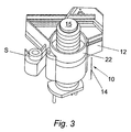
- Fig. 3 is a perspective view of the apparatus of Fig. 1 from one side, where a cover plate is positioned around the cylindrical circuit component;
- Fig. 4A is a transverse cross sectional view of the apparatus of Fig. 2; and
- Fig. 4B is a transverse cross sectional view of the apparatus of Fig. 2 with the cover plate positioned around the cylindrical circuit component.
- With reference to Fig. 2 circuit
component locating apparatus 10 includes afastening frame 12 having anextension 14 projecting therefrom. The fasteningframe 12 is in the form of a discrete frame member which can be attached to a circuit board with a number of locating rivets or screws S. Theextension 14 has an aperture therethrough which is shaped to accept a correspondinglyshaped circuit component 15. In the embodiment shown the aperture is circular in order to accept acylindrical circuit component 15, although it will be appreciated that the aperture could be any shape corresponding to a cross sectional shape of thecircuit component 15, for example, rectangular, square, triangular etc. The aperture is slightly larger than the circuit component around which it is to be placed in order to provide a space in which adhesive means, such as glue, may be provided. The size of the aperture can also be increased to aid positioning of the frame over thecircuit component 15 by accepting manufacturing tolerances in the dimensions of thecircuit component 15. - An attachment member, or wall W, is provided around the aperture and has a lip at the opening of the aperture. The lip is angled relative to the central axis of the aperture in order to form a
ledge 16. Theledge 16 is also contoured atlocations 18 in order to maintain a substantially constant space between the wall W and thecircuit component 15 taking account of anyprojecting connections 20 on thecircuit component 15. As shown in Fig. 2, a redundancy may be incorporated into the apparatus by providing thecontoured sections 18 at either side of thecomponent 15. This also allows the apparatus to fit properly over a component which is attached to the circuit board in the opposite direction (rotated through an angle of 180 degrees). - In use, the
apparatus 10 is placed over the various components of the circuit board, ensuring that each aperture of eachextension 14 is placed around each circuit component. Once in position over the circuit components, thefastening frame 12 is then secured to the circuit board by locating screws S. In order to secure, thecircuit components 15 to the fastening frame 12 (and hence relative to the circuit board) an adhesive is applied around theledge 16. The angle of theledge 16 is oriented such that the adhesive begins to flow toward thecomponent 15 and into engagement with both the inner side surface of the wall W and the outer side surface of thecircuit component 15 adjacent the wall W. In the present embodiment the ledge is angled at 45 degrees; however, any angle capable of providing the desired function may be used. - With reference to Fig. 3, some adhesives do not flow easily and may not flow into engagement with the circuit component. To overcome this, a
cover plate 22 is placed around thecircuit component 15. The cover plate may be a separate member or may be integrated into the apparatus by way of a hinge (not shown) which allows it to simply flip over the circuit component from a storage position to an active position. Thecover plate 22 is then progressed down the circuit component until a snap fit connection is formed between thecover plate 22 and thewall ledge 16. This causes any adhesive residing on theledge 16 to be pushed down into the space between the wall W andcircuit component 15. In this regard, the lower face of thecover plate 22 is shaped to correspond with the ledge of the wall W. The final position of the adhesive is referenced 24 in Fig. 4B. When in position, the cover plate also has the additional effect of sealing the top of the space between the wall and circuit component. Furthermore, the inner shape of the cover plate may be such that it fits closely around thecircuit component 15 and provides some additional lateral support to thecircuit component 15. - The apparatus described allows an adhesive connection to be provided between the side of the circuit component and the wall. With such an arrangement, the effect of any expansion and contraction of the adhesive on the soldered joints of the circuit component is minimised.
- The arrangement securely attaches the circuit components to the circuit board and therefore eliminates the need for securing the components using the casing. This further eliminates any stress on the circuit component soldered joints which would otherwise be caused by the interaction between the casing and the components during expansion and contraction.
- Modifications, and improvements may be made to the foregoing without departing from the scope of the invention, for example:-
- Although the apparatus in the embodiment shown in Figs. 2 to 4 is incorporated into a
discrete frame member 12, alternatively, the apparatus may be provided directly onto a circuit board.
Claims (13)
Priority Applications (4)
| Application Number | Priority Date | Filing Date | Title |
|---|---|---|---|
| EP06122447A EP1915043B1 (en) | 2006-10-17 | 2006-10-17 | Apparatus for fastening a component on a circuit board |
| DE602006009121T DE602006009121D1 (en) | 2006-10-17 | 2006-10-17 | Device for fixing an electrical component on a printed circuit board |
| AT06122447T ATE442766T1 (en) | 2006-10-17 | 2006-10-17 | DEVICE FOR FASTENING AN ELECTRICAL COMPONENT TO A CIRCUIT BOARD |
| US11/906,919 US20080086867A1 (en) | 2006-10-17 | 2007-10-04 | Circuit component locating apparatus |
Applications Claiming Priority (1)
| Application Number | Priority Date | Filing Date | Title |
|---|---|---|---|
| EP06122447A EP1915043B1 (en) | 2006-10-17 | 2006-10-17 | Apparatus for fastening a component on a circuit board |
Publications (2)
| Publication Number | Publication Date |
|---|---|
| EP1915043A1 true EP1915043A1 (en) | 2008-04-23 |
| EP1915043B1 EP1915043B1 (en) | 2009-09-09 |
Family
ID=37969937
Family Applications (1)
| Application Number | Title | Priority Date | Filing Date |
|---|---|---|---|
| EP06122447A Active EP1915043B1 (en) | 2006-10-17 | 2006-10-17 | Apparatus for fastening a component on a circuit board |
Country Status (4)
| Country | Link |
|---|---|
| US (1) | US20080086867A1 (en) |
| EP (1) | EP1915043B1 (en) |
| AT (1) | ATE442766T1 (en) |
| DE (1) | DE602006009121D1 (en) |
Families Citing this family (1)
| Publication number | Priority date | Publication date | Assignee | Title |
|---|---|---|---|---|
| CN113948319B (en) * | 2021-09-15 | 2023-07-21 | 南京高喜电子科技有限公司 | A kind of encapsulating equipment for electrolytic capacitors on integrated circuit boards |
Citations (4)
| Publication number | Priority date | Publication date | Assignee | Title |
|---|---|---|---|---|
| JPS63124556A (en) * | 1986-11-14 | 1988-05-28 | Hitachi Ltd | semiconductor package |
| WO1998037447A1 (en) * | 1997-02-18 | 1998-08-27 | Integrated Optical Components Limited | Carriers for optical components and methods of using the same |
| US20030093897A1 (en) * | 2001-11-16 | 2003-05-22 | Augustin Thomas J. | Method and apparatus for shock and vibration isolation of a circuit component |
| US20030103337A1 (en) * | 2001-12-05 | 2003-06-05 | Intel Corporation | Frame support for a printed board assembly |
Family Cites Families (4)
| Publication number | Priority date | Publication date | Assignee | Title |
|---|---|---|---|---|
| US4630875A (en) * | 1984-07-02 | 1986-12-23 | Amp Incorporated | Chip carrier socket which requires low insertion force for the chip carrier |
| US5612513A (en) * | 1995-09-19 | 1997-03-18 | Micron Communications, Inc. | Article and method of manufacturing an enclosed electrical circuit using an encapsulant |
| US7146721B2 (en) * | 2004-03-15 | 2006-12-12 | Delphi Technologies, Inc. | Method of manufacturing a sealed electronic module |
| US7652892B2 (en) * | 2006-03-03 | 2010-01-26 | Kingston Technology Corporation | Waterproof USB drives and method of making |
-
2006
- 2006-10-17 EP EP06122447A patent/EP1915043B1/en active Active
- 2006-10-17 DE DE602006009121T patent/DE602006009121D1/en active Active
- 2006-10-17 AT AT06122447T patent/ATE442766T1/en not_active IP Right Cessation
-
2007
- 2007-10-04 US US11/906,919 patent/US20080086867A1/en not_active Abandoned
Patent Citations (4)
| Publication number | Priority date | Publication date | Assignee | Title |
|---|---|---|---|---|
| JPS63124556A (en) * | 1986-11-14 | 1988-05-28 | Hitachi Ltd | semiconductor package |
| WO1998037447A1 (en) * | 1997-02-18 | 1998-08-27 | Integrated Optical Components Limited | Carriers for optical components and methods of using the same |
| US20030093897A1 (en) * | 2001-11-16 | 2003-05-22 | Augustin Thomas J. | Method and apparatus for shock and vibration isolation of a circuit component |
| US20030103337A1 (en) * | 2001-12-05 | 2003-06-05 | Intel Corporation | Frame support for a printed board assembly |
Also Published As
| Publication number | Publication date |
|---|---|
| EP1915043B1 (en) | 2009-09-09 |
| US20080086867A1 (en) | 2008-04-17 |
| DE602006009121D1 (en) | 2009-10-22 |
| ATE442766T1 (en) | 2009-09-15 |
Similar Documents
| Publication | Publication Date | Title |
|---|---|---|
| JP4741604B2 (en) | Control module | |
| JP6440865B2 (en) | Controller unit | |
| EP3073810B1 (en) | Electronic control unit with a housing stabilizing element and housing for electronic control unit | |
| JP2006512785A (en) | Electronic control unit | |
| CN107110341A (en) | Electronic-controlled installation | |
| JP2007506148A (en) | Optical module and optical system | |
| JP4186826B2 (en) | PCB mounting structure | |
| US8985539B2 (en) | Mounting bracket for electronic control modules | |
| US11115742B2 (en) | Microphone assembly and microphone arrangement | |
| US11332089B2 (en) | Supporting assembly | |
| CN113853837A (en) | Electronic control device | |
| JP6227937B2 (en) | Electronic control device for vehicle | |
| JP2008224428A (en) | Sensor device | |
| JP6121879B2 (en) | Controller unit | |
| US11201421B2 (en) | Printed circuit board mounting arrangement | |
| US9271399B2 (en) | Electronic module and method for the production thereof | |
| EP1915043A1 (en) | Apparatus for fastening a component on a circuit board | |
| US6770813B1 (en) | Mountable microelectronic package | |
| KR101081763B1 (en) | Windshield wiper, especially for a motor vehicle | |
| US20140365090A1 (en) | Control unit for a motor vehicle | |
| JP2019206295A (en) | On-vehicle electronic device | |
| CN102991465B (en) | Wiper part-fixed device and wiper device | |
| US7074058B2 (en) | Steel fuel flange with plastic strut mounts | |
| US5445450A (en) | Circuit board support | |
| JP6931962B2 (en) | Automotive antenna device |
Legal Events
| Date | Code | Title | Description |
|---|---|---|---|
| PUAI | Public reference made under article 153(3) epc to a published international application that has entered the european phase |
Free format text: ORIGINAL CODE: 0009012 |
|
| 17P | Request for examination filed |
Effective date: 20070622 |
|
| AK | Designated contracting states |
Kind code of ref document: A1 Designated state(s): AT BE BG CH CY CZ DE DK EE ES FI FR GB GR HU IE IS IT LI LT LU LV MC NL PL PT RO SE SI SK TR |
|
| AX | Request for extension of the european patent |
Extension state: AL BA HR MK RS |
|
| AKX | Designation fees paid |
Designated state(s): AT BE BG CH CY CZ DE DK EE ES FI FR GB GR HU IE IS IT LI LT LU LV MC NL PL PT RO SE SI SK TR |
|
| GRAP | Despatch of communication of intention to grant a patent |
Free format text: ORIGINAL CODE: EPIDOSNIGR1 |
|
| GRAS | Grant fee paid |
Free format text: ORIGINAL CODE: EPIDOSNIGR3 |
|
| GRAA | (expected) grant |
Free format text: ORIGINAL CODE: 0009210 |
|
| AK | Designated contracting states |
Kind code of ref document: B1 Designated state(s): AT BE BG CH CY CZ DE DK EE ES FI FR GB GR HU IE IS IT LI LT LU LV MC NL PL PT RO SE SI SK TR |
|
| REG | Reference to a national code |
Ref country code: GB Ref legal event code: FG4D |
|
| REG | Reference to a national code |
Ref country code: CH Ref legal event code: EP |
|
| REG | Reference to a national code |
Ref country code: IE Ref legal event code: FG4D |
|
| REF | Corresponds to: |
Ref document number: 602006009121 Country of ref document: DE Date of ref document: 20091022 Kind code of ref document: P |
|
| PG25 | Lapsed in a contracting state [announced via postgrant information from national office to epo] |
Ref country code: FI Free format text: LAPSE BECAUSE OF FAILURE TO SUBMIT A TRANSLATION OF THE DESCRIPTION OR TO PAY THE FEE WITHIN THE PRESCRIBED TIME-LIMIT Effective date: 20090909 Ref country code: SE Free format text: LAPSE BECAUSE OF FAILURE TO SUBMIT A TRANSLATION OF THE DESCRIPTION OR TO PAY THE FEE WITHIN THE PRESCRIBED TIME-LIMIT Effective date: 20090909 Ref country code: LT Free format text: LAPSE BECAUSE OF FAILURE TO SUBMIT A TRANSLATION OF THE DESCRIPTION OR TO PAY THE FEE WITHIN THE PRESCRIBED TIME-LIMIT Effective date: 20090909 |
|
| NLV1 | Nl: lapsed or annulled due to failure to fulfill the requirements of art. 29p and 29m of the patents act | ||
| LTIE | Lt: invalidation of european patent or patent extension |
Effective date: 20090909 |
|
| PG25 | Lapsed in a contracting state [announced via postgrant information from national office to epo] |
Ref country code: PL Free format text: LAPSE BECAUSE OF FAILURE TO SUBMIT A TRANSLATION OF THE DESCRIPTION OR TO PAY THE FEE WITHIN THE PRESCRIBED TIME-LIMIT Effective date: 20090909 Ref country code: LV Free format text: LAPSE BECAUSE OF FAILURE TO SUBMIT A TRANSLATION OF THE DESCRIPTION OR TO PAY THE FEE WITHIN THE PRESCRIBED TIME-LIMIT Effective date: 20090909 Ref country code: NL Free format text: LAPSE BECAUSE OF FAILURE TO SUBMIT A TRANSLATION OF THE DESCRIPTION OR TO PAY THE FEE WITHIN THE PRESCRIBED TIME-LIMIT Effective date: 20090909 Ref country code: SI Free format text: LAPSE BECAUSE OF FAILURE TO SUBMIT A TRANSLATION OF THE DESCRIPTION OR TO PAY THE FEE WITHIN THE PRESCRIBED TIME-LIMIT Effective date: 20090909 |
|
| PG25 | Lapsed in a contracting state [announced via postgrant information from national office to epo] |
Ref country code: CY Free format text: LAPSE BECAUSE OF FAILURE TO SUBMIT A TRANSLATION OF THE DESCRIPTION OR TO PAY THE FEE WITHIN THE PRESCRIBED TIME-LIMIT Effective date: 20090909 |
|
| PG25 | Lapsed in a contracting state [announced via postgrant information from national office to epo] |
Ref country code: IS Free format text: LAPSE BECAUSE OF FAILURE TO SUBMIT A TRANSLATION OF THE DESCRIPTION OR TO PAY THE FEE WITHIN THE PRESCRIBED TIME-LIMIT Effective date: 20100109 Ref country code: EE Free format text: LAPSE BECAUSE OF FAILURE TO SUBMIT A TRANSLATION OF THE DESCRIPTION OR TO PAY THE FEE WITHIN THE PRESCRIBED TIME-LIMIT Effective date: 20090909 Ref country code: RO Free format text: LAPSE BECAUSE OF FAILURE TO SUBMIT A TRANSLATION OF THE DESCRIPTION OR TO PAY THE FEE WITHIN THE PRESCRIBED TIME-LIMIT Effective date: 20090909 Ref country code: ES Free format text: LAPSE BECAUSE OF FAILURE TO SUBMIT A TRANSLATION OF THE DESCRIPTION OR TO PAY THE FEE WITHIN THE PRESCRIBED TIME-LIMIT Effective date: 20091220 Ref country code: PT Free format text: LAPSE BECAUSE OF FAILURE TO SUBMIT A TRANSLATION OF THE DESCRIPTION OR TO PAY THE FEE WITHIN THE PRESCRIBED TIME-LIMIT Effective date: 20100111 Ref country code: CZ Free format text: LAPSE BECAUSE OF FAILURE TO SUBMIT A TRANSLATION OF THE DESCRIPTION OR TO PAY THE FEE WITHIN THE PRESCRIBED TIME-LIMIT Effective date: 20090909 |
|
| PG25 | Lapsed in a contracting state [announced via postgrant information from national office to epo] |
Ref country code: MC Free format text: LAPSE BECAUSE OF NON-PAYMENT OF DUE FEES Effective date: 20091031 Ref country code: SK Free format text: LAPSE BECAUSE OF FAILURE TO SUBMIT A TRANSLATION OF THE DESCRIPTION OR TO PAY THE FEE WITHIN THE PRESCRIBED TIME-LIMIT Effective date: 20090909 |
|
| PG25 | Lapsed in a contracting state [announced via postgrant information from national office to epo] |
Ref country code: BE Free format text: LAPSE BECAUSE OF FAILURE TO SUBMIT A TRANSLATION OF THE DESCRIPTION OR TO PAY THE FEE WITHIN THE PRESCRIBED TIME-LIMIT Effective date: 20090909 Ref country code: AT Free format text: LAPSE BECAUSE OF FAILURE TO SUBMIT A TRANSLATION OF THE DESCRIPTION OR TO PAY THE FEE WITHIN THE PRESCRIBED TIME-LIMIT Effective date: 20090909 |
|
| PLBE | No opposition filed within time limit |
Free format text: ORIGINAL CODE: 0009261 |
|
| STAA | Information on the status of an ep patent application or granted ep patent |
Free format text: STATUS: NO OPPOSITION FILED WITHIN TIME LIMIT |
|
| PG25 | Lapsed in a contracting state [announced via postgrant information from national office to epo] |
Ref country code: DK Free format text: LAPSE BECAUSE OF FAILURE TO SUBMIT A TRANSLATION OF THE DESCRIPTION OR TO PAY THE FEE WITHIN THE PRESCRIBED TIME-LIMIT Effective date: 20090909 |
|
| 26N | No opposition filed |
Effective date: 20100610 |
|
| PG25 | Lapsed in a contracting state [announced via postgrant information from national office to epo] |
Ref country code: GR Free format text: LAPSE BECAUSE OF FAILURE TO SUBMIT A TRANSLATION OF THE DESCRIPTION OR TO PAY THE FEE WITHIN THE PRESCRIBED TIME-LIMIT Effective date: 20091210 Ref country code: IE Free format text: LAPSE BECAUSE OF NON-PAYMENT OF DUE FEES Effective date: 20091017 |
|
| PG25 | Lapsed in a contracting state [announced via postgrant information from national office to epo] |
Ref country code: BG Free format text: LAPSE BECAUSE OF FAILURE TO SUBMIT A TRANSLATION OF THE DESCRIPTION OR TO PAY THE FEE WITHIN THE PRESCRIBED TIME-LIMIT Effective date: 20091031 |
|
| PG25 | Lapsed in a contracting state [announced via postgrant information from national office to epo] |
Ref country code: LU Free format text: LAPSE BECAUSE OF NON-PAYMENT OF DUE FEES Effective date: 20091017 |
|
| REG | Reference to a national code |
Ref country code: CH Ref legal event code: PL |
|
| PG25 | Lapsed in a contracting state [announced via postgrant information from national office to epo] |
Ref country code: HU Free format text: LAPSE BECAUSE OF FAILURE TO SUBMIT A TRANSLATION OF THE DESCRIPTION OR TO PAY THE FEE WITHIN THE PRESCRIBED TIME-LIMIT Effective date: 20100310 |
|
| PG25 | Lapsed in a contracting state [announced via postgrant information from national office to epo] |
Ref country code: LI Free format text: LAPSE BECAUSE OF NON-PAYMENT OF DUE FEES Effective date: 20101031 Ref country code: CH Free format text: LAPSE BECAUSE OF NON-PAYMENT OF DUE FEES Effective date: 20101031 |
|
| PG25 | Lapsed in a contracting state [announced via postgrant information from national office to epo] |
Ref country code: TR Free format text: LAPSE BECAUSE OF FAILURE TO SUBMIT A TRANSLATION OF THE DESCRIPTION OR TO PAY THE FEE WITHIN THE PRESCRIBED TIME-LIMIT Effective date: 20090909 |
|
| REG | Reference to a national code |
Ref country code: FR Ref legal event code: PLFP Year of fee payment: 10 |
|
| REG | Reference to a national code |
Ref country code: FR Ref legal event code: PLFP Year of fee payment: 11 |
|
| REG | Reference to a national code |
Ref country code: FR Ref legal event code: PLFP Year of fee payment: 12 |
|
| REG | Reference to a national code |
Ref country code: FR Ref legal event code: PLFP Year of fee payment: 13 |
|
| REG | Reference to a national code |
Ref country code: DE Ref legal event code: R082 Ref document number: 602006009121 Country of ref document: DE Representative=s name: MANITZ FINSTERWALD PATENT- UND RECHTSANWALTSPA, DE Ref country code: DE Ref legal event code: R081 Ref document number: 602006009121 Country of ref document: DE Owner name: DELPHI TECHNOLOGIES IP LIMITED, BB Free format text: FORMER OWNER: DELPHI TECHNOLOGIES, INC., TROY, MICH., US |
|
| REG | Reference to a national code |
Ref country code: GB Ref legal event code: 732E Free format text: REGISTERED BETWEEN 20190214 AND 20190221 |
|
| P01 | Opt-out of the competence of the unified patent court (upc) registered |
Effective date: 20230327 |
|
| PGFP | Annual fee paid to national office [announced via postgrant information from national office to epo] |
Ref country code: GB Payment date: 20240912 Year of fee payment: 19 |
|
| PGFP | Annual fee paid to national office [announced via postgrant information from national office to epo] |
Ref country code: FR Payment date: 20240913 Year of fee payment: 19 |
|
| PGFP | Annual fee paid to national office [announced via postgrant information from national office to epo] |
Ref country code: DE Payment date: 20240913 Year of fee payment: 19 |
|
| PGFP | Annual fee paid to national office [announced via postgrant information from national office to epo] |
Ref country code: IT Payment date: 20241015 Year of fee payment: 19 |