EP1914797A2 - Method of manufacturing a lateral power mosfet - Google Patents
Method of manufacturing a lateral power mosfet Download PDFInfo
- Publication number
- EP1914797A2 EP1914797A2 EP07011477A EP07011477A EP1914797A2 EP 1914797 A2 EP1914797 A2 EP 1914797A2 EP 07011477 A EP07011477 A EP 07011477A EP 07011477 A EP07011477 A EP 07011477A EP 1914797 A2 EP1914797 A2 EP 1914797A2
- Authority
- EP
- European Patent Office
- Prior art keywords
- region
- forming
- conductivity type
- layer
- substrate
- Prior art date
- Legal status (The legal status is an assumption and is not a legal conclusion. Google has not performed a legal analysis and makes no representation as to the accuracy of the status listed.)
- Granted
Links
Images





Classifications
-
- H—ELECTRICITY
- H10—SEMICONDUCTOR DEVICES; ELECTRIC SOLID-STATE DEVICES NOT OTHERWISE PROVIDED FOR
- H10D—INORGANIC ELECTRIC SEMICONDUCTOR DEVICES
- H10D62/00—Semiconductor bodies, or regions thereof, of devices having potential barriers
- H10D62/10—Shapes, relative sizes or dispositions of the regions of the semiconductor bodies; Shapes of the semiconductor bodies
- H10D62/13—Semiconductor regions connected to electrodes carrying current to be rectified, amplified or switched, e.g. source or drain regions
- H10D62/149—Source or drain regions of field-effect devices
- H10D62/151—Source or drain regions of field-effect devices of IGFETs
-
- H—ELECTRICITY
- H10—SEMICONDUCTOR DEVICES; ELECTRIC SOLID-STATE DEVICES NOT OTHERWISE PROVIDED FOR
- H10P—GENERIC PROCESSES OR APPARATUS FOR THE MANUFACTURE OR TREATMENT OF DEVICES COVERED BY CLASS H10
- H10P10/00—Bonding of wafers, substrates or parts of devices
-
- H—ELECTRICITY
- H10—SEMICONDUCTOR DEVICES; ELECTRIC SOLID-STATE DEVICES NOT OTHERWISE PROVIDED FOR
- H10D—INORGANIC ELECTRIC SEMICONDUCTOR DEVICES
- H10D30/00—Field-effect transistors [FET]
- H10D30/01—Manufacture or treatment
- H10D30/021—Manufacture or treatment of FETs having insulated gates [IGFET]
- H10D30/0221—Manufacture or treatment of FETs having insulated gates [IGFET] having asymmetry in the channel direction, e.g. lateral high-voltage MISFETs having drain offset region or extended-drain MOSFETs [EDMOS]
-
- H—ELECTRICITY
- H10—SEMICONDUCTOR DEVICES; ELECTRIC SOLID-STATE DEVICES NOT OTHERWISE PROVIDED FOR
- H10D—INORGANIC ELECTRIC SEMICONDUCTOR DEVICES
- H10D30/00—Field-effect transistors [FET]
- H10D30/60—Insulated-gate field-effect transistors [IGFET]
- H10D30/601—Insulated-gate field-effect transistors [IGFET] having lightly-doped drain or source extensions, e.g. LDD IGFETs or DDD IGFETs
- H10D30/603—Insulated-gate field-effect transistors [IGFET] having lightly-doped drain or source extensions, e.g. LDD IGFETs or DDD IGFETs having asymmetry in the channel direction, e.g. lateral high-voltage MISFETs having drain offset region or extended drain IGFETs [EDMOS]
-
- H—ELECTRICITY
- H10—SEMICONDUCTOR DEVICES; ELECTRIC SOLID-STATE DEVICES NOT OTHERWISE PROVIDED FOR
- H10D—INORGANIC ELECTRIC SEMICONDUCTOR DEVICES
- H10D62/00—Semiconductor bodies, or regions thereof, of devices having potential barriers
- H10D62/10—Shapes, relative sizes or dispositions of the regions of the semiconductor bodies; Shapes of the semiconductor bodies
- H10D62/102—Constructional design considerations for preventing surface leakage or controlling electric field concentration
- H10D62/103—Constructional design considerations for preventing surface leakage or controlling electric field concentration for increasing or controlling the breakdown voltage of reverse-biased devices
- H10D62/105—Constructional design considerations for preventing surface leakage or controlling electric field concentration for increasing or controlling the breakdown voltage of reverse-biased devices by having particular doping profiles, shapes or arrangements of PN junctions; by having supplementary regions, e.g. junction termination extension [JTE]
- H10D62/109—Reduced surface field [RESURF] PN junction structures
-
- H—ELECTRICITY
- H10—SEMICONDUCTOR DEVICES; ELECTRIC SOLID-STATE DEVICES NOT OTHERWISE PROVIDED FOR
- H10D—INORGANIC ELECTRIC SEMICONDUCTOR DEVICES
- H10D62/00—Semiconductor bodies, or regions thereof, of devices having potential barriers
- H10D62/10—Shapes, relative sizes or dispositions of the regions of the semiconductor bodies; Shapes of the semiconductor bodies
- H10D62/102—Constructional design considerations for preventing surface leakage or controlling electric field concentration
- H10D62/103—Constructional design considerations for preventing surface leakage or controlling electric field concentration for increasing or controlling the breakdown voltage of reverse-biased devices
- H10D62/105—Constructional design considerations for preventing surface leakage or controlling electric field concentration for increasing or controlling the breakdown voltage of reverse-biased devices by having particular doping profiles, shapes or arrangements of PN junctions; by having supplementary regions, e.g. junction termination extension [JTE]
- H10D62/109—Reduced surface field [RESURF] PN junction structures
- H10D62/111—Multiple RESURF structures, e.g. double RESURF or 3D-RESURF structures
-
- H—ELECTRICITY
- H10—SEMICONDUCTOR DEVICES; ELECTRIC SOLID-STATE DEVICES NOT OTHERWISE PROVIDED FOR
- H10D—INORGANIC ELECTRIC SEMICONDUCTOR DEVICES
- H10D62/00—Semiconductor bodies, or regions thereof, of devices having potential barriers
- H10D62/10—Shapes, relative sizes or dispositions of the regions of the semiconductor bodies; Shapes of the semiconductor bodies
- H10D62/13—Semiconductor regions connected to electrodes carrying current to be rectified, amplified or switched, e.g. source or drain regions
- H10D62/149—Source or drain regions of field-effect devices
- H10D62/151—Source or drain regions of field-effect devices of IGFETs
- H10D62/156—Drain regions of DMOS transistors
- H10D62/157—Impurity concentrations or distributions
-
- H—ELECTRICITY
- H10—SEMICONDUCTOR DEVICES; ELECTRIC SOLID-STATE DEVICES NOT OTHERWISE PROVIDED FOR
- H10D—INORGANIC ELECTRIC SEMICONDUCTOR DEVICES
- H10D64/00—Electrodes of devices having potential barriers
- H10D64/20—Electrodes characterised by their shapes, relative sizes or dispositions
- H10D64/27—Electrodes not carrying the current to be rectified, amplified, oscillated or switched, e.g. gates
- H10D64/311—Gate electrodes for field-effect devices
- H10D64/411—Gate electrodes for field-effect devices for FETs
- H10D64/511—Gate electrodes for field-effect devices for FETs for IGFETs
- H10D64/514—Gate electrodes for field-effect devices for FETs for IGFETs characterised by the insulating layers
- H10D64/516—Gate electrodes for field-effect devices for FETs for IGFETs characterised by the insulating layers the thicknesses being non-uniform
Definitions
- This invention relates generally to semiconductor structures and methods, and more particularly to a lateral power metal oxide semiconductor field effect transistor (MOSFET).
- MOSFET metal oxide semiconductor field effect transistor
- a lateral power MOSFET is basically a metal oxide semiconductor field effect transistor fabricated with coplanar drain and source regions.
- Figure 1A shows a lateral power MOSFET device 100 in the prior art.
- the device 100 is formed on a p-type substrate 101 and another p-layer 113 is epitaxially grown on the substrate 101.
- a high-voltage P-well 115 is adjacent a high-voltage N-well 103 in the epitaxially grown p-layer 113.
- An N+ source 117 is positioned in the high-voltage P-well 115 such that the N+ source 117 is not immediately adjacent the high-voltage N-well 103, and an N+ drain 105 is positioned in the high-voltage N-well 103.
- Dielectrics 121 are formed to isolate and define areas such as the N+ source 117 and the N+ drain 105 of the device 100.
- a gate dielectric 111 and a gate electrode 110 are formed extending from the source 117 to a portion of the field dielectric 107.
- the device 100 also includes a P+ area 119 located in the high-voltage P-well 115. Applying a positive voltage to the gate electrode 110 induces a current to flow through the channel from the N+ source 117 into the high-voltage N-well 103 to be collected at the N+ drain 105.
- a problem with this type of lateral power MOSFET is that it cannot maintain a low on-resistance when a high voltage is passed through the lateral power MOSFET.
- the on-resistance is the power of the current that is transformed into heat as the current travels through the device.
- the larger the on-resistance of the device the less efficient the device. Accordingly, it is desired to reduce this resistance as much as possible for a more efficient device.
- Figure 1B illustrates another device 150 known in the prior that is designed to mitigate this problem.
- Device 150 is similar to device 100 of Figure 1A, wherein like reference numerals refer to like elements, except a field ring 109 has been added.
- the field ring 109 works to reduce the surface electrical field and improves the depletion capability of the drift region. As a result, the doping concentration of the drift region can be increased and the on-resistance of the device 100 can be decreased.
- the breakdown voltage is the voltage at which a normally high-resistance element (such as a MOS capacitor or reverse biased p-n junction) allows current to flow.
- a normally high-resistance element such as a MOS capacitor or reverse biased p-n junction
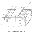
- Figure 2 is a lateral power MOSFET designed to increase the breakdown voltage of the device 200.
- the field dielectrics have been removed from view for clarity.
- partition regions 201 have been placed into the high-voltage N-well 103, as shown in Figure 2, such that there are areas of alternating conductivity in the high-voltage N-well region. This type of configuration is known in the art as a superjunction.
- the partition regions 201 work to increase the horizontal depletion capability of the drift region, which allows for a higher concentration of doping in the drift region. This helps to increase the breakdown voltage and works to reduce the specific on-resistance of the device.
- One aspect of the present invention is a semiconductor device that has a substrate with an extended drift region that has a first conductivity type.
- a first region of the first conductivity type is located above the extended drift region.
- a second region of first semiconductor material is located adjacent to, and forms a junction with, the first region, to form the channel of the device.
- Field dielectrics are located over the first region and the second region.
- a gate dielectric and a gate electrode overlie and extend from a portion of the field dielectric to a portion of the second region.
- source and drain regions are located within the first and second regions.
- Another aspect of the present invention is a lateral power metal oxide semiconductor that is similar to the device described above, but additionally includes a field ring located under the field dielectric.
- the field ring has the second conductivity type.
- Yet another aspect of the present invention is a lateral power superjunction metal oxide semiconductor field effect transistor.
- This embodiment is similar to the previously described first embodiment (including the extended drift region). However, a plurality of partition regions of second conductivity type is located in the first region. This plurality of partition regions is arranged in the first region in such a way as to form alternating areas of opposite conductivity in the first region, in order to form a superjunction.
- Figure 1A is a cross-sectional view of a lateral power MOSFET in the prior art
- Figure 1B is a cross-sectional view of a lateral power MOSFET with a field ring in the prior art
- Figure 2 is a perspective view of a lateral power superjunction MOSFET in the prior art
- Figures 3A-3G are cross-sectional views of various steps of a method of manufacturing of a MOSFET in which an extended drift region is incorporated into a lateral power MOSFET, in accordance with an embodiment of the present invention
- Figures 4A-4D are cross-sectional views of various stages of a method of manufacturing of a MOSFET in which an extended drift region is incorporated into a lateral power MOSFET that has a field ring, in accordance with an embodiment of the present invention
- Figures 5A-5E are cross-sectional views of various steps of a method of manufacturing of a lateral power superjunction MOSFET in which an extended drift region is incorporated into a lateral power superjunction MOSFET, in accordance with an embodiment of the present invention
- Figure 6 is a comparison chart of the on-resistance versus the depth of the drift region in an embodiment of the present invention and traditional lateral power MOSFETS;
- Figure 7 is a comparison of the breakdown voltage versus the depth of the drift region in an embodiment of the present invention and traditional lateral power MOSFETS.
- the present invention is a semiconductor device with a reduced on-resistance and an increased breakdown voltage when the device is under a large voltage.
- Embodiments of the present invention may be useful for lateral power MOSFETs, particularly when the device is under a large voltage.
- a voltage of about 800 V is large.
- voltages greater than or less than 800 V may be considered large in other embodiments of the present invention.
- the manufacturing process of this device is detailed in the following paragraphs.
- a substrate 301 is provided in accordance with an embodiment of the present invention.
- the substrate 301 may comprise bulk silicon, doped or undoped, or an active layer of a silicon-on-insulator (SOI) substrate.
- SOI substrate comprises a layer of a semiconductor material such as silicon, germanium, silicon germanium, SOI, silicon germanium on insulator (SGOI), or combinations thereof.
- Other substrates that may be used include multi-layered substrates, gradient substrates, or hybrid orientation substrates.
- NBL N+ buried layer
- the NBL 303 is preferably formed by implanting n-type dopants into the upper region of the substrate 301.
- the NBL 303 may be formed by implanting an n-type dopant such as phosphorous at a concentration of between about 3 x 10 15 and about 3 x 10 16 , and a voltage level of between about 20 to about 200 keV.
- n-type dopants such as arsenic, nitrogen, antimony, combinations thereof, or the like could alternatively be used.
- the n-type dopant of the NBL 303 may then be driven into the substrate 301 by heating the substrate 301 to a temperature of about 1,000 °C to about 1,200 °C.
- the NBL 303 formed preferably comprises a thickness of between about 2 ⁇ m and 10 ⁇ m, and more preferably has a thickness of about 6 ⁇ m, for example.
- FIG. 3B illustrates a doped semiconductor material 305 being formed over the substrate 301 and the NBL 303 in accordance with an embodiment of the present invention.
- the doped semiconductor material 305 preferably comprises a P-type semiconductor such as silicon.
- the doped semiconductor material 305 is preferably formed epitaxially, although other methods may alternatively be used.
- the doped semiconductor material 305 is referred to herein as a P-epi layer or P-epitaxial layer.
- the P-epi layer 305 is formed in a thickness between about 2 ⁇ m and about 5 ⁇ m, and more preferably to a thickness of about 4 ⁇ m in an embodiment; however, other thicknesses may be used.
- the P-epi layer 305 may be doped with boron, for example, although other p-type dopants such as gallium, aluminum, indium, combinations thereof, or the like may alternatively be used.
- FIG. 3C illustrates the formation of a high-voltage N-well region 307 in accordance with an embodiment of the present invention.
- the high-voltage N-well region 307 may be formed by implanting an n-type dopant such as phosphorous to a concentration of about 3 x 10 15 to about 3 x 10 16 dopant concentration at about 180 KeV, for example.
- an n-type dopant such as phosphorous
- other n-type dopants such as arsenic, nitrogen, antimony, combinations thereof, or the like, could alternatively be used.
- the high-voltage N-well region 307 has a thickness of about between about 4 ⁇ m and about 10 ⁇ m, and a preferred thickness of 4 ⁇ m.
- Figure 3D illustrates the formation of the high-voltage P-well 309 in accordance with an embodiment of the present invention.
- the high-voltage P-well 309 is formed substantially adjacent to the high-voltage N-well 307, such that a junction between the two wells is created.
- the high-voltage P-well 309 may be formed by doping at least a portion of the P-epi layer 305 with a p-type dopant such as boron at a concentration of between about 1 x 10 15 to about 2 x 10 16 at a power of about 100 keV, as an example.
- the high-voltage P-well 309 has a depth of between about 2 ⁇ m to about 6 ⁇ m, with a preferred depth of about 4 ⁇ m.
- other p-type dopants such as gallium, aluminum, indium, combinations thereof, or the like could alternatively be used.
- Figure 3E illustrates the formation of a first field dielectric 311 and a group of second field dielectrics 313 in accordance with an embodiment of the present invention.
- the first field dielectric 311 is formed over a portion of the high-voltage N-well 307.
- the second field dielectrics 313 are formed over portions of the high-voltage P-well 309 and the P-epi layer 305, as shown in Figure 3E.
- the first field dielectric 311 and the second field dielectric 313 are preferably formed simultaneously.
- the first field dielectric 311 and second field dielectric 313 may comprise silicon dioxide, formed by patterning a masking layer (not shown) to expose portions of the substrate 301 at which the first field dielectric 311 and the second field dielectrics 313 are desired, heating the substrate 301 in the presence of oxygen at a temperature of about 980 °C, and then removing the masking layer.
- the first field dielectric 311 and the second field dielectric 313 preferably comprise a thickness of between about 3,000 ⁇ and about 7,000 ⁇ , with a preferred thickness of about 5,000 ⁇ , for example. However, the first field dielectric 311 and second field dielectric 313 may alternately comprise other thicknesses and materials.
- Figure 3F shows the formation of a gate dielectric 314 and a gate conductor 315 in accordance with an embodiment of the present invention.
- the gate dielectric 314 is deposited over an upper portion of the field dielectric 311 and extends to cover portions of the high-voltage P-well region 309.
- a gate conductor 315 is deposited over the gate dielectric 314.
- the gate conductor 315 comprises a conductive layer such as a doped polysilicon, metal, metal alloy or the like.
- a surface of the gate conductor 315 may be silicided.
- Figure 3G illustrates the formation of a source region 319 in the high-voltage P-well region 309 and a drain region 317 in the high-voltage N-well region 307.
- the source region 319 and the drain region 317 can be formed by implanting an n-type dopant such as phosphorous at a concentration of between about 1 x 10 19 and about 2 x 10 20 at about 80 KeV, as examples.
- an n-type dopant such as phosphorous at a concentration of between about 1 x 10 19 and about 2 x 10 20 at about 80 KeV, as examples.
- other n-type dopants such as arsenic, nitrogen, antimony, combinations thereof, or the like could alternatively be used.
- Figure 3G also shows the formation of a P+ region 321 that can be formed in the high-voltage P-well region 309.
- the p-type dopant may be boron implanted at a concentration of between about 1 x 10 19 and about 2 x 10 20 at about 70 keV, as an example.
- Other p-type dopants such as gallium, aluminum, indium, combinations thereof, or the like could alternatively be used.
- the dimensions and dopant concentrations of the substrate 301, the NBL 303, and the high-voltage N-well region 307 can be set in accordance with the reduced surface field (RESURF) technique, such that the substrate 301, the NBL 303, and the high-voltage N-well region 307 form a single RESURF structure, as is known in the art.
- RESURF reduced surface field
- This structure reduces the electric field at the junction of the high-voltage P-well 309 and the high-voltage N-well 307, and allows for an even larger increased breakdown voltage of the overall device.
- Figures 4A to 4C illustrate another embodiment of the present invention, in which a lateral power MOSFET that has a field ring is manufactured with an extended drift region in accordance with an embodiment of the present invention.
- the initial steps of the manufacturing process are similar to those shown in Figures 3A through 3D, wherein like reference numerals refer to like elements.
- Figure 4A illustrates that a portion of the high-voltage N-well 307 is counter-doped with a p-type dopant to form a field ring 401.
- the field ring 401 may be formed by doping a portion of the high-voltage N-well 307 with a p-type dopant such as boron to a depth of between about 0.4 ⁇ m to about 2 ⁇ m, with a preferred depth of about 1 ⁇ m.
- a p-type dopant such as boron
- other p-type dopants such as gallium, aluminum, indium, combinations thereof, or the like could alternatively be used.
- Figure 4B illustrates the formation of a first field dielectric 311 and a group of second field dielectrics 313 in accordance with an embodiment of the present invention.
- the first field dielectric 311 is formed over the field ring 401 and a portion of the high-voltage N-well 307.
- the second field dielectrics 313 are formed over portions of the high-voltage P-well 309 and the P-epi layer 305, as shown in Figure 4B.
- the first field dielectric 311 and second field dielectric 313 may be formed as discussed above with reference to Figure 3E.
- Figure 4C shows the formation of a gate dielectric 314 and a gate electrode 315 in accordance with an embodiment of the present invention.
- the gate dielectric 314 is deposited over the top surface of the field dielectric 311 and extends to cover a portion of the high-voltage P-well region 309, as shown in Figure 4C.
- a gate electrode 315 is deposited over the gate dielectric 314.
- the gate electrode 315 and gate dielectric 314 may be formed as discussed above with reference to Figure 3F.
- Figure 4D illustrates the formation of a source region 319 in the high-voltage P-well region 309 and a drain region 317 in the high-voltage N-well region 307 in accordance with an embodiment of the present invention.
- the source and drain regions may be formed as discussed above with reference to Figure 3G.
- Figure 4D also shows the formation of a P+ region 321 that will be formed in the high-voltage P-well region in accordance with an embodiment of the present invention.
- the P+ region 321 may be formed as discussed above with reference to Figure 3G.
- the dimensions and dopant concentrations of the substrate 301, the NBL 303, the high-voltage N-well region 307, and the field ring 401 can be set in accordance with the reduced surface field (RESURF) technique, such that the substrate 301, the NBL 303, the high-voltage N-well region 307, and the field ring 401 form a double RESURF structure, as is known in the art.
- RESURF reduced surface field
- Figures 5A-5E illustrate yet another embodiment of the present invention, in which a lateral power superjunction MOSFET is manufactured with an extended drift region.
- the initial steps of manufacturing this embodiment are similar to the methods as shown through Figures 3A-3D.
- Figure 5A illustrates that, prior to the formation of the field dielectric 311, partition regions 501 are formed in the high-voltage N-well region 307 to form a superjunction MOSFET, as is known in the art.
- the partition regions are p-type conductive regions.
- partition regions 501 can be formed through ion implantation of a p-type dopant such as boron at a concentration of between about 1 x 10 15 and about 2 x 10 16 at a power of about 70 keV and a subsequent thermal drive in.
- a p-type dopant such as boron
- other p-type dopants such as gallium, aluminum, indium, combinations thereof, or the like could alternatively be used.
- the partition regions 501 have a depth of between about 0.5 ⁇ m and about 5 ⁇ m, with a preferred depth of about 3 ⁇ m.
- Figure 5B illustrates another view of the superjunction partition regions 501 taken along the 5B-5B axis in Figure 5A.
- the partition regions 501 are interspaced within the high-voltage N-well region 307 to form alternating areas of opposite conductivity.
- the partition regions 501 preferably extend substantially through the P-epi layer 305 and do not extend into the NBL 303.
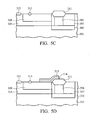
- Figure 5C illustrates the formation of a first field dielectric 311 and a group of second field dielectrics 313 once the partition regions 501 are formed in accordance with an embodiment of the present invention.
- Figure 5C is a cross-sectional view taken along the 5C-5C axis in Figure 5A after the formation of a first field dielectric 311 and second field dielectrics 313.
- the first field dielectric 311 is formed over a portion of the high-voltage N-well 307 and portions of the partition regions 501.
- the second field dielectrics 313 are formed over portions of the high-voltage P-well 309 and the P-epi layer 305, as shown in Figure 5B.
- the first field dielectric 311 may be formed as discussed above with reference to Figure 3E.
- Figure 5D shows the device of Figure 5C after the formation of a gate dielectric 314 and a gate electrode 315 in accordance with an embodiment of the present invention.
- the gate dielectric 314 is deposited over the top surface of the field dielectric 311 and extends to cover portions of the high-voltage P-well region 309, as shown in Figure 5C.
- the gate electrode 315 and gate dielectric 314 may be formed as discussed above with reference to Figure 3F.
- Figure 5E illustrates the device of Figure 5D after the formation of a source region 319 in the high-voltage P-well region 309 and a drain region 317 in the high-voltage N-well region 307 in accordance with an embodiment of the present invention.
- the source region 319 and drain region 317 may be formed as discussed above with reference to Figure 3G.
- Figure 5E also shows the formation of a P+ region 321 that will be formed in the high-voltage P-well region.
- the P+ region 321 may be formed as discussed above with reference to Figure 3G.
- Figure 6 is a chart that shows a comparison of the on resistance of a semiconductor device in relation to the depth of the drift region between an embodiment of the present invention and a traditional semiconductor device. As shown, an increase in the depth of the drift region from about 4 ⁇ m to about 10 ⁇ m may translate to about a 65% improvement of the on-resistance of the device.
- Figure 7 is a chart that shows a comparison of the breakdown voltage of a semiconductor device in relation to the depth of the drift region between the present invention and a traditional semiconductor device. As shown, an increase in the depth of the drift region from about 4 ⁇ m to about 10 ⁇ m may lead to about a 15% improvement in the breakdown voltage over traditional lateral power MOSFETs.
- embodiments as presented herein are merely illustrative embodiments of the present invention.
- the discussed embodiment is a p-type lateral power MOSFET
- another embodiment could be an n-type lateral power MOSFET, with a n-type channel region, p-type source and drain regions, and a p-type extended drift region.
Landscapes
- Insulated Gate Type Field-Effect Transistor (AREA)
Abstract
Description
- This invention relates generally to semiconductor structures and methods, and more particularly to a lateral power metal oxide semiconductor field effect transistor (MOSFET).
- A lateral power MOSFET is basically a metal oxide semiconductor field effect transistor fabricated with coplanar drain and source regions. Figure 1A shows a lateral
power MOSFET device 100 in the prior art. Thedevice 100 is formed on a p-type substrate 101 and another p-layer 113 is epitaxially grown on thesubstrate 101. A high-voltage P-well 115 is adjacent a high-voltage N-well 103 in the epitaxially grown p-layer 113. AnN+ source 117 is positioned in the high-voltage P-well 115 such that theN+ source 117 is not immediately adjacent the high-voltage N-well 103, and anN+ drain 105 is positioned in the high-voltage N-well 103.Dielectrics 121 are formed to isolate and define areas such as theN+ source 117 and theN+ drain 105 of thedevice 100. A gate dielectric 111 and agate electrode 110 are formed extending from thesource 117 to a portion of the field dielectric 107. Thedevice 100 also includes aP+ area 119 located in the high-voltage P-well 115. Applying a positive voltage to thegate electrode 110 induces a current to flow through the channel from theN+ source 117 into the high-voltage N-well 103 to be collected at theN+ drain 105. - A problem with this type of lateral power MOSFET is that it cannot maintain a low on-resistance when a high voltage is passed through the lateral power MOSFET. The on-resistance is the power of the current that is transformed into heat as the current travels through the device. The larger the on-resistance of the device, the less efficient the device. Accordingly, it is desired to reduce this resistance as much as possible for a more efficient device.
- Figure 1B illustrates another
device 150 known in the prior that is designed to mitigate this problem.Device 150 is similar todevice 100 of Figure 1A, wherein like reference numerals refer to like elements, except afield ring 109 has been added. Thefield ring 109 works to reduce the surface electrical field and improves the depletion capability of the drift region. As a result, the doping concentration of the drift region can be increased and the on-resistance of thedevice 100 can be decreased. - Another problem with the prior art device 100 (shown in Figure 1A) and the prior art device 150 (shown in Figure 1B) is that the breakdown voltage is not as high as desired. The breakdown voltage is the voltage at which a normally high-resistance element (such as a MOS capacitor or reverse biased p-n junction) allows current to flow. When voltage larger than the breakdown voltage is passed through devices such as
device 100 anddevice 150, catastrophic and irreversible damage is done to the devices, rendering the devices commercially useless and requiring the devices to be replaced. Accordingly, increasing the breakdown voltage is highly desirable. - Figure 2 is a lateral power MOSFET designed to increase the breakdown voltage of the
device 200. In Figure 2 the field dielectrics have been removed from view for clarity. In thisdevice 200partition regions 201 have been placed into the high-voltage N-well 103, as shown in Figure 2, such that there are areas of alternating conductivity in the high-voltage N-well region. This type of configuration is known in the art as a superjunction. Thepartition regions 201 work to increase the horizontal depletion capability of the drift region, which allows for a higher concentration of doping in the drift region. This helps to increase the breakdown voltage and works to reduce the specific on-resistance of the device. - Those prior art systems, however, have difficulties sustaining high voltage and low on-resistance, thus, an improved lateral power MOSFET is needed for a reduced on-resistance and a higher breakdown voltage when the device is placed under a high voltage.
- These and other problems are generally solved or circumvented, and technical advantages are generally achieved, by embodiments of the present invention that allow for an extended drift region in a lateral power MOSFET that has a reduced on-resistance and an increased breakdown voltage when the device is placed under high voltage.
- One aspect of the present invention is a semiconductor device that has a substrate with an extended drift region that has a first conductivity type. A first region of the first conductivity type is located above the extended drift region. A second region of first semiconductor material is located adjacent to, and forms a junction with, the first region, to form the channel of the device. Field dielectrics are located over the first region and the second region. A gate dielectric and a gate electrode overlie and extend from a portion of the field dielectric to a portion of the second region. Finally, source and drain regions are located within the first and second regions.
- Another aspect of the present invention is a lateral power metal oxide semiconductor that is similar to the device described above, but additionally includes a field ring located under the field dielectric. The field ring has the second conductivity type.
- Yet another aspect of the present invention is a lateral power superjunction metal oxide semiconductor field effect transistor. This embodiment is similar to the previously described first embodiment (including the extended drift region). However, a plurality of partition regions of second conductivity type is located in the first region. This plurality of partition regions is arranged in the first region in such a way as to form alternating areas of opposite conductivity in the first region, in order to form a superjunction.
- By using these configurations in semiconductor devices and lateral power MOSFETs that have an extended drift region, the on-resistance of the device is reduced and the breakdown voltage of the device is increased. These all work to improve the performance and efficiency of the semiconductor device.
- For a more complete understanding of the present invention, and the advantages thereof, reference is now made to the following descriptions taken in conjunction with the accompanying drawing, in which:
- Figure 1A is a cross-sectional view of a lateral power MOSFET in the prior art;
- Figure 1B is a cross-sectional view of a lateral power MOSFET with a field ring in the prior art;
- Figure 2 is a perspective view of a lateral power superjunction MOSFET in the prior art;
- Figures 3A-3G are cross-sectional views of various steps of a method of manufacturing of a MOSFET in which an extended drift region is incorporated into a lateral power MOSFET, in accordance with an embodiment of the present invention;
- Figures 4A-4D are cross-sectional views of various stages of a method of manufacturing of a MOSFET in which an extended drift region is incorporated into a lateral power MOSFET that has a field ring, in accordance with an embodiment of the present invention;
- Figures 5A-5E are cross-sectional views of various steps of a method of manufacturing of a lateral power superjunction MOSFET in which an extended drift region is incorporated into a lateral power superjunction MOSFET, in accordance with an embodiment of the present invention;
- Figure 6 is a comparison chart of the on-resistance versus the depth of the drift region in an embodiment of the present invention and traditional lateral power MOSFETS; and
- Figure 7 is a comparison of the breakdown voltage versus the depth of the drift region in an embodiment of the present invention and traditional lateral power MOSFETS.
- The making and using of the presently preferred embodiments are discussed in detail below. It should be appreciated, however, that the present invention provides many applicable inventive concepts that can be embodied in a wide variety of specific contexts. The specific embodiments discussed are merely illustrative of specific ways to make and use the invention, and do not limit the scope of the invention.
- The present invention is a semiconductor device with a reduced on-resistance and an increased breakdown voltage when the device is under a large voltage. Embodiments of the present invention may be useful for lateral power MOSFETs, particularly when the device is under a large voltage. In an embodiment discussed herein, a voltage of about 800 V is large. However, voltages greater than or less than 800 V may be considered large in other embodiments of the present invention. The manufacturing process of this device is detailed in the following paragraphs.
- Referring first to Figure 3A, a
substrate 301 is provided in accordance with an embodiment of the present invention. Thesubstrate 301 may comprise bulk silicon, doped or undoped, or an active layer of a silicon-on-insulator (SOI) substrate. Generally, an SOI substrate comprises a layer of a semiconductor material such as silicon, germanium, silicon germanium, SOI, silicon germanium on insulator (SGOI), or combinations thereof. Other substrates that may be used include multi-layered substrates, gradient substrates, or hybrid orientation substrates. - An N+ buried layer (NBL) 303 is formed in a portion of the
substrate 301 proximate the top surface of thesubstrate 301. TheNBL 303 is preferably formed by implanting n-type dopants into the upper region of thesubstrate 301. For example, theNBL 303 may be formed by implanting an n-type dopant such as phosphorous at a concentration of between about 3 x 10¹⁵ and about 3 x 10¹⁶, and a voltage level of between about 20 to about 200 keV. However, other n-type dopants, such as arsenic, nitrogen, antimony, combinations thereof, or the like could alternatively be used. The n-type dopant of theNBL 303 may then be driven into thesubstrate 301 by heating thesubstrate 301 to a temperature of about 1,000 °C to about 1,200 °C. TheNBL 303 formed preferably comprises a thickness of between about 2 µm and 10 µm, and more preferably has a thickness of about 6 µm, for example. - Figure 3B illustrates a doped
semiconductor material 305 being formed over thesubstrate 301 and theNBL 303 in accordance with an embodiment of the present invention. The dopedsemiconductor material 305 preferably comprises a P-type semiconductor such as silicon. The dopedsemiconductor material 305 is preferably formed epitaxially, although other methods may alternatively be used. The dopedsemiconductor material 305 is referred to herein as a P-epi layer or P-epitaxial layer. Preferably, the P-epi layer 305 is formed in a thickness between about 2 µm and about 5 µm, and more preferably to a thickness of about 4 µm in an embodiment; however, other thicknesses may be used. The P-epi layer 305 may be doped with boron, for example, although other p-type dopants such as gallium, aluminum, indium, combinations thereof, or the like may alternatively be used. - Figure 3C illustrates the formation of a high-voltage N-
well region 307 in accordance with an embodiment of the present invention. The high-voltage N-well region 307 may be formed by implanting an n-type dopant such as phosphorous to a concentration of about 3 x 10¹⁵ to about 3 x 10¹⁶ dopant concentration at about 180 KeV, for example. However, other n-type dopants such as arsenic, nitrogen, antimony, combinations thereof, or the like, could alternatively be used. In an embodiment, the high-voltage N-well region 307 has a thickness of about between about 4 µm and about 10 µm, and a preferred thickness of 4 µm. - Figure 3D illustrates the formation of the high-voltage P-well 309 in accordance with an embodiment of the present invention. Preferably, the high-voltage P-well 309 is formed substantially adjacent to the high-voltage N-well 307, such that a junction between the two wells is created. The high-voltage P-well 309 may be formed by doping at least a portion of the P-
epi layer 305 with a p-type dopant such as boron at a concentration of between about 1 x 10¹⁵ to about 2 x 10¹⁶ at a power of about 100 keV, as an example. In an embodiment, the high-voltage P-well 309 has a depth of between about 2 µm to about 6 µm, with a preferred depth of about 4 µm. However, other p-type dopants such as gallium, aluminum, indium, combinations thereof, or the like could alternatively be used. - Figure 3E illustrates the formation of a
first field dielectric 311 and a group ofsecond field dielectrics 313 in accordance with an embodiment of the present invention. Thefirst field dielectric 311 is formed over a portion of the high-voltage N-well 307. Thesecond field dielectrics 313 are formed over portions of the high-voltage P-well 309 and the P-epi layer 305, as shown in Figure 3E. In an embodiment of the present invention thefirst field dielectric 311 and thesecond field dielectric 313 are preferably formed simultaneously. Thefirst field dielectric 311 andsecond field dielectric 313 may comprise silicon dioxide, formed by patterning a masking layer (not shown) to expose portions of thesubstrate 301 at which thefirst field dielectric 311 and thesecond field dielectrics 313 are desired, heating thesubstrate 301 in the presence of oxygen at a temperature of about 980 °C, and then removing the masking layer. Thefirst field dielectric 311 and thesecond field dielectric 313 preferably comprise a thickness of between about 3,000 Å and about 7,000 Å, with a preferred thickness of about 5,000 Å, for example. However, thefirst field dielectric 311 andsecond field dielectric 313 may alternately comprise other thicknesses and materials. - Figure 3F shows the formation of a
gate dielectric 314 and agate conductor 315 in accordance with an embodiment of the present invention. Thegate dielectric 314 is deposited over an upper portion of thefield dielectric 311 and extends to cover portions of the high-voltage P-well region 309. Agate conductor 315 is deposited over thegate dielectric 314. Thegate conductor 315 comprises a conductive layer such as a doped polysilicon, metal, metal alloy or the like. Optionally, a surface of thegate conductor 315 may be silicided. - Figure 3G illustrates the formation of a
source region 319 in the high-voltage P-well region 309 and adrain region 317 in the high-voltage N-well region 307. Thesource region 319 and thedrain region 317 can be formed by implanting an n-type dopant such as phosphorous at a concentration of between about 1 x 10¹⁹ and about 2 x 10²⁰ at about 80 KeV, as examples. However, other n-type dopants such as arsenic, nitrogen, antimony, combinations thereof, or the like could alternatively be used. - Figure 3G also shows the formation of a
P+ region 321 that can be formed in the high-voltage P-well region 309. The p-type dopant may be boron implanted at a concentration of between about 1 x 10¹⁹ and about 2 x 10²⁰ at about 70 keV, as an example. Other p-type dopants such as gallium, aluminum, indium, combinations thereof, or the like could alternatively be used. - Optionally, the dimensions and dopant concentrations of the
substrate 301, theNBL 303, and the high-voltage N-well region 307 can be set in accordance with the reduced surface field (RESURF) technique, such that thesubstrate 301, theNBL 303, and the high-voltage N-well region 307 form a single RESURF structure, as is known in the art. This structure reduces the electric field at the junction of the high-voltage P-well 309 and the high-voltage N-well 307, and allows for an even larger increased breakdown voltage of the overall device. - Figures 4A to 4C illustrate another embodiment of the present invention, in which a lateral power MOSFET that has a field ring is manufactured with an extended drift region in accordance with an embodiment of the present invention. In this embodiment the initial steps of the manufacturing process are similar to those shown in Figures 3A through 3D, wherein like reference numerals refer to like elements. However, Figure 4A illustrates that a portion of the high-voltage N-well 307 is counter-doped with a p-type dopant to form a
field ring 401. Thefield ring 401 may be formed by doping a portion of the high-voltage N-well 307 with a p-type dopant such as boron to a depth of between about 0.4 µm to about 2 µm, with a preferred depth of about 1 µm. However, other p-type dopants such as gallium, aluminum, indium, combinations thereof, or the like could alternatively be used. - Figure 4B illustrates the formation of a
first field dielectric 311 and a group ofsecond field dielectrics 313 in accordance with an embodiment of the present invention. Thefirst field dielectric 311 is formed over thefield ring 401 and a portion of the high-voltage N-well 307. Thesecond field dielectrics 313 are formed over portions of the high-voltage P-well 309 and the P-epi layer 305, as shown in Figure 4B. Thefirst field dielectric 311 andsecond field dielectric 313 may be formed as discussed above with reference to Figure 3E. - Figure 4C shows the formation of a
gate dielectric 314 and agate electrode 315 in accordance with an embodiment of the present invention. Thegate dielectric 314 is deposited over the top surface of thefield dielectric 311 and extends to cover a portion of the high-voltage P-well region 309, as shown in Figure 4C. Agate electrode 315 is deposited over thegate dielectric 314. Thegate electrode 315 andgate dielectric 314 may be formed as discussed above with reference to Figure 3F. - Figure 4D illustrates the formation of a
source region 319 in the high-voltage P-well region 309 and adrain region 317 in the high-voltage N-well region 307 in accordance with an embodiment of the present invention. The source and drain regions may be formed as discussed above with reference to Figure 3G. - Figure 4D also shows the formation of a
P+ region 321 that will be formed in the high-voltage P-well region in accordance with an embodiment of the present invention. TheP+ region 321 may be formed as discussed above with reference to Figure 3G. - Optionally, the dimensions and dopant concentrations of the
substrate 301, theNBL 303, the high-voltage N-well region 307, and thefield ring 401 can be set in accordance with the reduced surface field (RESURF) technique, such that thesubstrate 301, theNBL 303, the high-voltage N-well region 307, and thefield ring 401 form a double RESURF structure, as is known in the art. This structure reduces the electric field at the junction of the high-voltage P-well 309 and the high-voltage N-well 307, and allows for an even larger increased breakdown voltage of the overall device. - Figures 5A-5E illustrate yet another embodiment of the present invention, in which a lateral power superjunction MOSFET is manufactured with an extended drift region. The initial steps of manufacturing this embodiment are similar to the methods as shown through Figures 3A-3D. Figure 5A illustrates that, prior to the formation of the
field dielectric 311,partition regions 501 are formed in the high-voltage N-well region 307 to form a superjunction MOSFET, as is known in the art. In this embodiment the partition regions are p-type conductive regions. Thesepartition regions 501 can be formed through ion implantation of a p-type dopant such as boron at a concentration of between about 1 x 10¹⁵ and about 2 x 10¹⁶ at a power of about 70 keV and a subsequent thermal drive in. However, other p-type dopants such as gallium, aluminum, indium, combinations thereof, or the like could alternatively be used. In an embodiment thepartition regions 501 have a depth of between about 0.5 µm and about 5 µm, with a preferred depth of about 3 µm. - Figure 5B illustrates another view of the
superjunction partition regions 501 taken along the 5B-5B axis in Figure 5A. In this view, it is shown that thepartition regions 501 are interspaced within the high-voltage N-well region 307 to form alternating areas of opposite conductivity. Thepartition regions 501 preferably extend substantially through the P-epi layer 305 and do not extend into theNBL 303. - Figure 5C illustrates the formation of a
first field dielectric 311 and a group ofsecond field dielectrics 313 once thepartition regions 501 are formed in accordance with an embodiment of the present invention. Figure 5C is a cross-sectional view taken along the 5C-5C axis in Figure 5A after the formation of afirst field dielectric 311 andsecond field dielectrics 313. Thefirst field dielectric 311 is formed over a portion of the high-voltage N-well 307 and portions of thepartition regions 501. Thesecond field dielectrics 313 are formed over portions of the high-voltage P-well 309 and the P-epi layer 305, as shown in Figure 5B. Thefirst field dielectric 311 may be formed as discussed above with reference to Figure 3E. - Figure 5D shows the device of Figure 5C after the formation of a
gate dielectric 314 and agate electrode 315 in accordance with an embodiment of the present invention. Thegate dielectric 314 is deposited over the top surface of thefield dielectric 311 and extends to cover portions of the high-voltage P-well region 309, as shown in Figure 5C. Thegate electrode 315 andgate dielectric 314 may be formed as discussed above with reference to Figure 3F. - Figure 5E illustrates the device of Figure 5D after the formation of a
source region 319 in the high-voltage P-well region 309 and adrain region 317 in the high-voltage N-well region 307 in accordance with an embodiment of the present invention. Thesource region 319 and drainregion 317 may be formed as discussed above with reference to Figure 3G. - Figure 5E also shows the formation of a
P+ region 321 that will be formed in the high-voltage P-well region. TheP+ region 321 may be formed as discussed above with reference to Figure 3G. - Figure 6 is a chart that shows a comparison of the on resistance of a semiconductor device in relation to the depth of the drift region between an embodiment of the present invention and a traditional semiconductor device. As shown, an increase in the depth of the drift region from about 4 µm to about 10 µm may translate to about a 65% improvement of the on-resistance of the device.
- Figure 7 is a chart that shows a comparison of the breakdown voltage of a semiconductor device in relation to the depth of the drift region between the present invention and a traditional semiconductor device. As shown, an increase in the depth of the drift region from about 4 µm to about 10 µm may lead to about a 15% improvement in the breakdown voltage over traditional lateral power MOSFETs.
- As one of ordinary skill in the art will appreciate, embodiments as presented herein are merely illustrative embodiments of the present invention. For example, while the discussed embodiment is a p-type lateral power MOSFET, another embodiment could be an n-type lateral power MOSFET, with a n-type channel region, p-type source and drain regions, and a p-type extended drift region.
- Although the present invention and its advantages have been described in detail, it should be understood that various changes, substitutions and alterations can be made herein without departing from the spirit and scope of the invention as defined by the appended claims. For example, there are multiple methods for the deposition of material as the structure is being formed. Any of these deposition methods that achieve substantially the same result as the corresponding embodiments described herein may be utilized according to the present invention.
- Moreover, the scope of the present application is not intended to be limited to the particular embodiments of the methods described in the specification. As one of ordinary skill in the art will readily appreciate from the disclosure of the present invention, methods presently existing, or later to be developed, that perform substantially the same function or achieve substantially the same result as the corresponding embodiments described herein may be utilized according to the present invention. Accordingly, the appended claims are intended to include within their scope such methods.
Claims (10)
- A method of forming a semiconductor device, the method comprising:providing a substrate with a first layer;forming an extended drift region in an upper region of a portion of the first layer, the extended drift region comprising a first conductivity type;forming a second layer over the extended drift region and the substrate;forming a first region within the second layer and over the extended drift region, the first region comprising the first conductivity type;forming a second region within the second layer and substantially adjacent to the first region in a plane that is substantially parallel to a major surface of the substrate, the second region comprising a second conductivity type;forming a field dielectric over a portion of the first region; andforming a gate dielectric and gate electrode such that the gate dielectric and gate electrode extend from over a portion of the field dielectric to over a portion of the second region.
- The method of claim 1, wherein the first layer is epitaxially grown on the substrate.
- The method of claim 1, wherein the substrate, the extended drift region, and the first region have dimensions set according to the reduced surface field (RESURF) technique to form a single RESURF structure.
- A method of forming a lateral diffused metal oxide semiconductor (LDMOS) device, the method comprising:providing a substrate with a first layer;forming an extended drift region in the top region of a portion of the first layer, the extended drift region comprising a first conductivity type;forming a second layer over the extended drift region and the substrate;forming a first region within the second layer and substantially aligned with the extended drift region, the first region comprising the first conductivity type;forming a second region within the second layer and having a junction with the first region, the second region having a second conductivity type;forming a drain region in the first region, the drain region having the first conductivity type;forming a source region in the second region, the source region having the first conductivity type;forming a field ring in the first region, interposed between, but not substantially adjacent to, the drain region and the second region, the field ring having a second conductivity type;forming a field dielectric over a portion of the first region; andforming a gate dielectric and gate electrode, such that the gate dielectric and gate electrode extend from over a portion of the field dielectric to over a portion of the second region.
- The method of claim 4, wherein the first layer is epitaxially grown on the substrate.
- The method of claim 4, wherein the substrate, the first region, the second region, and the fourth region have dimensions set according to the reduced surface field (RESURF) technique to form a double RESURF structure.
- A method of forming a lateral diffused superjunction metal oxide semiconductor (LDMOS) device, the method comprising:providing a substrate with a first layer;forming an extended drift region in a portion of the substrate, the extended drift region comprising a first conductivity type;forming a second layer over the extended drift region and the substrate;forming a first region within the second layer above and substantially aligned with the extended drift region, the first region comprising the first conductivity type;forming a second region within the second layer and having a junction with the first region, the second region comprising a second conductivity type;forming a drain region in the first region, the drain region having the first conductivity type;forming a source region in the second region, the source region having the first conductivity type;forming partition regions in the first region, the partition regions having the second conductivity type, such that the partition regions and the first region form areas of alternating conductivity type;forming a field dielectric over a portion of the first region; andforming a gate dielectric and gate electrode, such that the gate dielectric and gate electrode extend from over a portion of the field dielectric to over a portion of the second region.
- The method of claim 7, wherein the first conductivity type is a p-type semiconductor conductivity, and the second conductivity type is an n-type conductivity.
- The method of claim 7, wherein the first conductivity type is an n-type conductivity, and the second conductivity type is a p-type conductivity.
- The method of claim 7, wherein the first layer is epitaxially grown on the substrate and the extended drift region.
Applications Claiming Priority (1)
| Application Number | Priority Date | Filing Date | Title |
|---|---|---|---|
| US11/581,178 US7476591B2 (en) | 2006-10-13 | 2006-10-13 | Lateral power MOSFET with high breakdown voltage and low on-resistance |
Publications (3)
| Publication Number | Publication Date |
|---|---|
| EP1914797A2 true EP1914797A2 (en) | 2008-04-23 |
| EP1914797A3 EP1914797A3 (en) | 2009-08-12 |
| EP1914797B1 EP1914797B1 (en) | 2015-08-12 |
Family
ID=38820350
Family Applications (1)
| Application Number | Title | Priority Date | Filing Date |
|---|---|---|---|
| EP07011477.2A Active EP1914797B1 (en) | 2006-10-13 | 2007-06-12 | Method of manufacturing a lateral semiconductor device |
Country Status (4)
| Country | Link |
|---|---|
| US (2) | US7476591B2 (en) |
| EP (1) | EP1914797B1 (en) |
| KR (1) | KR100878509B1 (en) |
| CN (1) | CN101162697A (en) |
Cited By (2)
| Publication number | Priority date | Publication date | Assignee | Title |
|---|---|---|---|---|
| CN102110712B (en) * | 2009-12-23 | 2012-06-27 | 旺宏电子股份有限公司 | Lateral power metal oxide semiconductor field effect transistor structure and manufacturing method |
| US12154983B2 (en) | 2019-09-19 | 2024-11-26 | Csmc Technologies Fab2 Co., Ltd. | Lateral double-diffused metal oxide semiconductor device and manufacturing method thereof, and electronic apparatus |
Families Citing this family (51)
| Publication number | Priority date | Publication date | Assignee | Title |
|---|---|---|---|---|
| US7989890B2 (en) | 2006-10-13 | 2011-08-02 | Taiwan Semiconductor Manufacturing Company, Ltd. | Lateral power MOSFET with high breakdown voltage and low on-resistance |
| US9484451B2 (en) | 2007-10-05 | 2016-11-01 | Vishay-Siliconix | MOSFET active area and edge termination area charge balance |
| US7768071B2 (en) * | 2008-07-09 | 2010-08-03 | Taiwan Semiconductor Manufacturing Company, Ltd. | Stabilizing breakdown voltages by forming tunnels for ultra-high voltage devices |
| US7960786B2 (en) * | 2008-07-09 | 2011-06-14 | Taiwan Semiconductor Manufacturing Company, Ltd. | Breakdown voltages of ultra-high voltage devices by forming tunnels |
| US8445955B2 (en) * | 2009-02-27 | 2013-05-21 | Taiwan Semiconductor Manufacturing Company, Ltd. | Quasi-vertical structure for high voltage MOS device |
| TWI487105B (en) * | 2009-12-16 | 2015-06-01 | Macronix Int Co Ltd | Lateral power metal oxide semiconductor field effect transistor structure and manufacturing method thereof |
| US8247992B2 (en) * | 2010-03-23 | 2012-08-21 | Green Mark Technology Inc. | LED driver circuit |
| DE102010014370B4 (en) * | 2010-04-09 | 2021-12-02 | X-Fab Semiconductor Foundries Ag | LDMOS transistor and LDMOS component |
| US8772871B2 (en) * | 2010-08-20 | 2014-07-08 | Freescale Semiconductor, Inc. | Partially depleted dielectric resurf LDMOS |
| TWI405271B (en) * | 2010-12-30 | 2013-08-11 | Anpec Electronics Corp | Method of manufacturing power semiconductor device with super junction |
| CN102651318A (en) * | 2011-02-23 | 2012-08-29 | 旺宏电子股份有限公司 | Method for manufacturing high-voltage transistor |
| US8367511B2 (en) | 2011-03-07 | 2013-02-05 | Macronix International Co., Ltd. | Manufacturing method for high voltage transistor |
| CN102769028B (en) * | 2011-05-03 | 2015-01-28 | 旺宏电子股份有限公司 | Semiconductor structure and manufacturing method thereof |
| TWI478336B (en) * | 2011-05-06 | 2015-03-21 | 漢磊科技股份有限公司 | Structure for reducing surface electric field and lateral double-diffused MOS device |
| US9431249B2 (en) * | 2011-12-01 | 2016-08-30 | Vishay-Siliconix | Edge termination for super junction MOSFET devices |
| US9614043B2 (en) | 2012-02-09 | 2017-04-04 | Vishay-Siliconix | MOSFET termination trench |
| US9299773B2 (en) | 2012-02-20 | 2016-03-29 | Macronix International Co., Ltd. | Semiconductor structure and method for forming the same |
| CN103258845B (en) * | 2012-02-21 | 2015-09-09 | 旺宏电子股份有限公司 | Semiconductor structure and forming method thereof |
| US20130270636A1 (en) * | 2012-04-17 | 2013-10-17 | Broadcom Corporation | Transistor Having An Isolated Body For High Voltage Operation |
| US8853780B2 (en) * | 2012-05-07 | 2014-10-07 | Freescale Semiconductor, Inc. | Semiconductor device with drain-end drift diminution |
| US9842911B2 (en) | 2012-05-30 | 2017-12-12 | Vishay-Siliconix | Adaptive charge balanced edge termination |
| US9653459B2 (en) * | 2012-07-03 | 2017-05-16 | Taiwan Semiconductor Manufacturing Company, Ltd. | MOSFET having source region formed in a double wells region |
| US9070576B2 (en) | 2012-09-07 | 2015-06-30 | Freescale Semiconductor Inc. | Semiconductor device and related fabrication methods |
| US8748981B2 (en) * | 2012-09-07 | 2014-06-10 | Freescale Semiconductor, Inc. | Semiconductor device and related fabrication methods |
| US8779555B2 (en) * | 2012-12-06 | 2014-07-15 | Taiwan Semiconductor Manufacturing Co., Ltd. | Partial SOI on power device for breakdown voltage improvement |
| US9698024B2 (en) | 2012-12-06 | 2017-07-04 | Taiwan Semiconductor Manufacturing Co., Ltd. | Partial SOI on power device for breakdown voltage improvement |
| KR101976481B1 (en) | 2012-12-20 | 2019-05-10 | 삼성전자주식회사 | Semiconductor device and method for fabricating the same |
| US9490322B2 (en) | 2013-01-23 | 2016-11-08 | Freescale Semiconductor, Inc. | Semiconductor device with enhanced 3D resurf |
| US9070766B1 (en) * | 2014-01-27 | 2015-06-30 | Macronix International Co., Ltd. | Semiconductor device and method of forming the same |
| US9543379B2 (en) | 2014-03-18 | 2017-01-10 | Nxp Usa, Inc. | Semiconductor device with peripheral breakdown protection |
| WO2015171873A1 (en) * | 2014-05-07 | 2015-11-12 | Cambridge Electronics, Inc. | Transistor structure having buried island regions |
| US9245754B2 (en) | 2014-05-28 | 2016-01-26 | Mark E. Granahan | Simplified charge balance in a semiconductor device |
| US9508596B2 (en) | 2014-06-20 | 2016-11-29 | Vishay-Siliconix | Processes used in fabricating a metal-insulator-semiconductor field effect transistor |
| US9887259B2 (en) | 2014-06-23 | 2018-02-06 | Vishay-Siliconix | Modulated super junction power MOSFET devices |
| CN106575666B (en) | 2014-08-19 | 2021-08-06 | 维西埃-硅化物公司 | Superjunction Metal Oxide Semiconductor Field Effect Transistor |
| US9385229B2 (en) | 2014-09-24 | 2016-07-05 | Freescale Semiconductor, Inc. | Semiconductor device with improved breakdown voltage |
| US9306060B1 (en) | 2014-11-20 | 2016-04-05 | Freescale Semiconductor Inc. | Semiconductor devices and related fabrication methods |
| KR102272382B1 (en) | 2014-11-21 | 2021-07-05 | 삼성전자주식회사 | Semiconductor device |
| CN105070759A (en) * | 2015-08-31 | 2015-11-18 | 上海华虹宏力半导体制造有限公司 | Nldmos device and manufacturing method thereof |
| CN105448995A (en) * | 2015-12-31 | 2016-03-30 | 上海华虹宏力半导体制造有限公司 | NLDMOS device and process method |
| US9871135B2 (en) | 2016-06-02 | 2018-01-16 | Nxp Usa, Inc. | Semiconductor device and method of making |
| US9905687B1 (en) | 2017-02-17 | 2018-02-27 | Nxp Usa, Inc. | Semiconductor device and method of making |
| CN107910358B (en) * | 2017-11-06 | 2020-09-25 | 上海华虹宏力半导体制造有限公司 | LDMOS (laterally diffused metal oxide semiconductor) and manufacturing method thereof |
| US10510831B2 (en) * | 2018-02-19 | 2019-12-17 | Globalfoundries Singapore Pte. Ltd. | Low on resistance high voltage metal oxide semiconductor transistor |
| CN110459602A (en) * | 2019-08-31 | 2019-11-15 | 电子科技大学 | Device with vertical floating field plate and method of making the same |
| CN110518059B (en) * | 2019-08-31 | 2021-01-22 | 电子科技大学 | Longitudinal floating field plate device with charge balance withstand voltage layer and manufacturing method thereof |
| CN111969043A (en) * | 2020-08-28 | 2020-11-20 | 电子科技大学 | High-voltage three-dimensional depletion super junction LDMOS device and manufacturing method thereof |
| TW202240906A (en) * | 2021-04-13 | 2022-10-16 | 新唐科技股份有限公司 | Semiconductor device |
| CN114122113B (en) * | 2022-01-27 | 2022-05-03 | 江苏游隼微电子有限公司 | High-reliability MOSFET power semiconductor device structure |
| US20250006836A1 (en) * | 2023-06-29 | 2025-01-02 | Texas Instruments Incorporated | Semiconductor device with nitrogen doped field relief dielectric layer |
| CN117766588B (en) * | 2024-02-22 | 2024-04-30 | 南京邮电大学 | Super junction dual SOI-LDMOS device with extended drain structure and manufacturing method |
Family Cites Families (23)
| Publication number | Priority date | Publication date | Assignee | Title |
|---|---|---|---|---|
| US5306652A (en) * | 1991-12-30 | 1994-04-26 | Texas Instruments Incorporated | Lateral double diffused insulated gate field effect transistor fabrication process |
| US5322804A (en) * | 1992-05-12 | 1994-06-21 | Harris Corporation | Integration of high voltage lateral MOS devices in low voltage CMOS architecture using CMOS-compatible process steps |
| US5378912A (en) * | 1993-11-10 | 1995-01-03 | Philips Electronics North America Corporation | Lateral semiconductor-on-insulator (SOI) semiconductor device having a lateral drift region |
| JP3250419B2 (en) * | 1994-06-15 | 2002-01-28 | 株式会社デンソー | Semiconductor device and manufacturing method thereof |
| US6800903B2 (en) | 1996-11-05 | 2004-10-05 | Power Integrations, Inc. | High-voltage transistor with multi-layer conduction region |
| JP3382163B2 (en) * | 1998-10-07 | 2003-03-04 | 株式会社東芝 | Power semiconductor device |
| JP2000252465A (en) | 1999-03-03 | 2000-09-14 | Sony Corp | Semiconductor device and manufacturing method thereof |
| US6265752B1 (en) * | 1999-05-25 | 2001-07-24 | Taiwan Semiconductor Manufacturing, Co., Inc. | Method of forming a HVNMOS with an N+ buried layer combined with N well and a structure of the same |
| TW521437B (en) * | 2000-10-19 | 2003-02-21 | Sanyo Electric Co | Semiconductor device and process thereof |
| US6486034B1 (en) * | 2001-07-20 | 2002-11-26 | Taiwan Semiconductor Manufacturing Company | Method of forming LDMOS device with double N-layering |
| JP3935042B2 (en) * | 2002-04-26 | 2007-06-20 | 株式会社東芝 | Insulated gate semiconductor device |
| KR100867574B1 (en) * | 2002-05-09 | 2008-11-10 | 페어차일드코리아반도체 주식회사 | High voltage device and manufacturing method thereof |
| US7719054B2 (en) | 2006-05-31 | 2010-05-18 | Advanced Analogic Technologies, Inc. | High-voltage lateral DMOS device |
| US6919598B2 (en) * | 2003-03-10 | 2005-07-19 | Zia Hossain | LDMOS transistor with enhanced termination region for high breakdown voltage with low on-resistance |
| US6924531B2 (en) * | 2003-10-01 | 2005-08-02 | Taiwan Semiconductor Manufacturing Company, Ltd. | LDMOS device with isolation guard rings |
| US6873011B1 (en) | 2004-02-24 | 2005-03-29 | System General Corp. | High voltage and low on-resistance LDMOS transistor having equalized capacitance |
| US7202531B2 (en) | 2004-04-16 | 2007-04-10 | Matsushita Electric Industrial Co., Ltd. | Semiconductor device |
| TWI229933B (en) | 2004-06-25 | 2005-03-21 | Novatek Microelectronics Corp | High voltage device for electrostatic discharge protective circuit and high voltage device |
| US8080848B2 (en) | 2006-05-11 | 2011-12-20 | Fairchild Semiconductor Corporation | High voltage semiconductor device with lateral series capacitive structure |
| US7508032B2 (en) | 2007-02-20 | 2009-03-24 | Taiwan Semiconductor Manufacturing Co., Ltd. | High voltage device with low on-resistance |
| US7893490B2 (en) | 2007-04-30 | 2011-02-22 | Taiwan Semiconductor Manufacturing Company, Ltd. | HVNMOS structure for reducing on-resistance and preventing BJT triggering |
| US8168466B2 (en) | 2007-06-01 | 2012-05-01 | Semiconductor Components Industries, Llc | Schottky diode and method therefor |
| US7709908B2 (en) | 2007-08-10 | 2010-05-04 | United Microelectronics Corp. | High-voltage MOS transistor device |
-
2006
- 2006-10-13 US US11/581,178 patent/US7476591B2/en active Active
-
2007
- 2007-05-18 CN CNA2007101033125A patent/CN101162697A/en active Pending
- 2007-06-12 EP EP07011477.2A patent/EP1914797B1/en active Active
- 2007-06-29 KR KR1020070065721A patent/KR100878509B1/en active Active
-
2008
- 2008-12-05 US US12/329,285 patent/US8129783B2/en active Active
Non-Patent Citations (2)
| Title |
|---|
| KER M-D ET AL.: "Double Snapback Characteristics in High-Voltage nMOSFETs and the Impact to On-Chip ESD Protection Design", IEEE ELECTRON DEVICE LETTERS, IEEE SERVICE CENTER, vol. 25, no. 9, 1 September 2004 (2004-09-01), pages 640 - 642 |
| RAMEZANI M ET AL.: "A MONOLIGHIC IGBT GATE DRIVER IMPLEMENTED IN A CONVENTIONAL 0.8MUM BICMOS PROCESS", PROCEEDINGS OF THE 10TH INTERNATIONAL SYMPOSIUM ON POWER SEMICONDUCTOR DEVICES & IC'S. ISPSD '98, 3 June 1998 (1998-06-03), pages 109 - 112 |
Cited By (2)
| Publication number | Priority date | Publication date | Assignee | Title |
|---|---|---|---|---|
| CN102110712B (en) * | 2009-12-23 | 2012-06-27 | 旺宏电子股份有限公司 | Lateral power metal oxide semiconductor field effect transistor structure and manufacturing method |
| US12154983B2 (en) | 2019-09-19 | 2024-11-26 | Csmc Technologies Fab2 Co., Ltd. | Lateral double-diffused metal oxide semiconductor device and manufacturing method thereof, and electronic apparatus |
Also Published As
| Publication number | Publication date |
|---|---|
| US20090085101A1 (en) | 2009-04-02 |
| US7476591B2 (en) | 2009-01-13 |
| KR20080033843A (en) | 2008-04-17 |
| EP1914797A3 (en) | 2009-08-12 |
| US20080090347A1 (en) | 2008-04-17 |
| US8129783B2 (en) | 2012-03-06 |
| CN101162697A (en) | 2008-04-16 |
| EP1914797B1 (en) | 2015-08-12 |
| KR100878509B1 (en) | 2009-01-13 |
Similar Documents
| Publication | Publication Date | Title |
|---|---|---|
| US7476591B2 (en) | Lateral power MOSFET with high breakdown voltage and low on-resistance | |
| US7989890B2 (en) | Lateral power MOSFET with high breakdown voltage and low on-resistance | |
| US7508032B2 (en) | High voltage device with low on-resistance | |
| US8772871B2 (en) | Partially depleted dielectric resurf LDMOS | |
| US7602037B2 (en) | High voltage semiconductor devices and methods for fabricating the same | |
| US7960786B2 (en) | Breakdown voltages of ultra-high voltage devices by forming tunnels | |
| EP2680312B1 (en) | High breakdown voltage LDMOS device | |
| EP1946378B1 (en) | Method of manufacturing a semiconductor device | |
| CN100524809C (en) | A field effect transistor semiconductor device | |
| US7602014B2 (en) | Superjunction power MOSFET | |
| US7928508B2 (en) | Disconnected DPW structures for improving on-state performance of MOS devices | |
| US9269808B2 (en) | Method and apparatus for power device with depletion structure | |
| US20020053695A1 (en) | Split buried layer for high voltage LDMOS transistor | |
| US20110008944A1 (en) | Gate Electrodes of HVMOS Devices Having Non-Uniform Doping Concentrations | |
| US8592923B2 (en) | Coupling well structure for improving HVMOS performance | |
| US9478456B2 (en) | Semiconductor device with composite drift region | |
| US20100006933A1 (en) | Stabilizing Breakdown Voltages by Forming Tunnels for Ultra-High Voltage Devices | |
| US20080265292A1 (en) | Novel HVNMOS structure for reducing on-resistance and preventing BJT triggering | |
| US8963218B2 (en) | Dual-gate VDMOS device | |
| US20210043735A1 (en) | Short channel trench power mosfet and method | |
| US8471334B2 (en) | Lateral power MOSFET device having a liner layer formed along the current path to reduce electric resistance and method for manufacturing the same | |
| EP3998638A1 (en) | Laterally diffused metal oxide semiconductor device and manufacturing method therefor | |
| US20220285488A1 (en) | Superjunction semiconductor device having floating region and method of manufacturing same | |
| EP4517828A1 (en) | Edge termination region of superjunction device | |
| US20090121286A1 (en) | Integrated Circuit Comprising a Field Effect Transistor and Method of Fabricating the Same |
Legal Events
| Date | Code | Title | Description |
|---|---|---|---|
| PUAI | Public reference made under article 153(3) epc to a published international application that has entered the european phase |
Free format text: ORIGINAL CODE: 0009012 |
|
| AK | Designated contracting states |
Kind code of ref document: A2 Designated state(s): AT BE BG CH CY CZ DE DK EE ES FI FR GB GR HU IE IS IT LI LT LU LV MC MT NL PL PT RO SE SI SK TR |
|
| AX | Request for extension of the european patent |
Extension state: AL BA HR MK RS |
|
| PUAL | Search report despatched |
Free format text: ORIGINAL CODE: 0009013 |
|
| AK | Designated contracting states |
Kind code of ref document: A3 Designated state(s): AT BE BG CH CY CZ DE DK EE ES FI FR GB GR HU IE IS IT LI LT LU LV MC MT NL PL PT RO SE SI SK TR |
|
| AX | Request for extension of the european patent |
Extension state: AL BA HR MK RS |
|
| 17P | Request for examination filed |
Effective date: 20091116 |
|
| 17Q | First examination report despatched |
Effective date: 20091210 |
|
| AKX | Designation fees paid |
Designated state(s): DE NL |
|
| GRAP | Despatch of communication of intention to grant a patent |
Free format text: ORIGINAL CODE: EPIDOSNIGR1 |
|
| INTG | Intention to grant announced |
Effective date: 20150119 |
|
| GRAS | Grant fee paid |
Free format text: ORIGINAL CODE: EPIDOSNIGR3 |
|
| GRAA | (expected) grant |
Free format text: ORIGINAL CODE: 0009210 |
|
| AK | Designated contracting states |
Kind code of ref document: B1 Designated state(s): DE NL |
|
| REG | Reference to a national code |
Ref country code: DE Ref legal event code: R096 Ref document number: 602007042502 Country of ref document: DE |
|
| REG | Reference to a national code |
Ref country code: NL Ref legal event code: FP |
|
| REG | Reference to a national code |
Ref country code: DE Ref legal event code: R097 Ref document number: 602007042502 Country of ref document: DE |
|
| PLBE | No opposition filed within time limit |
Free format text: ORIGINAL CODE: 0009261 |
|
| STAA | Information on the status of an ep patent application or granted ep patent |
Free format text: STATUS: NO OPPOSITION FILED WITHIN TIME LIMIT |
|
| 26N | No opposition filed |
Effective date: 20160513 |
|
| REG | Reference to a national code |
Ref country code: DE Ref legal event code: R079 Ref document number: 602007042502 Country of ref document: DE Free format text: PREVIOUS MAIN CLASS: H01L0021336000 Ipc: H10D0030010000 |
|
| PGFP | Annual fee paid to national office [announced via postgrant information from national office to epo] |
Ref country code: DE Payment date: 20250627 Year of fee payment: 19 |
|
| PGFP | Annual fee paid to national office [announced via postgrant information from national office to epo] |
Ref country code: NL Payment date: 20250626 Year of fee payment: 19 |