EP1909322A1 - Stacked electronic component, electronic device and method for manufacturing stacked electronic component - Google Patents
Stacked electronic component, electronic device and method for manufacturing stacked electronic component Download PDFInfo
- Publication number
- EP1909322A1 EP1909322A1 EP06766961A EP06766961A EP1909322A1 EP 1909322 A1 EP1909322 A1 EP 1909322A1 EP 06766961 A EP06766961 A EP 06766961A EP 06766961 A EP06766961 A EP 06766961A EP 1909322 A1 EP1909322 A1 EP 1909322A1
- Authority
- EP
- European Patent Office
- Prior art keywords
- electronic component
- resin layer
- multilayer electronic
- columnar conductor
- ceramic substrate
- Prior art date
- Legal status (The legal status is an assumption and is not a legal conclusion. Google has not performed a legal analysis and makes no representation as to the accuracy of the status listed.)
- Withdrawn
Links
Images


Classifications
-
- H—ELECTRICITY
- H10—SEMICONDUCTOR DEVICES; ELECTRIC SOLID-STATE DEVICES NOT OTHERWISE PROVIDED FOR
- H10W—GENERIC PACKAGES, INTERCONNECTIONS, CONNECTORS OR OTHER CONSTRUCTIONAL DETAILS OF DEVICES COVERED BY CLASS H10
- H10W90/00—Package configurations
- H10W90/701—Package configurations characterised by the relative positions of pads or connectors relative to package parts
-
- H—ELECTRICITY
- H05—ELECTRIC TECHNIQUES NOT OTHERWISE PROVIDED FOR
- H05K—PRINTED CIRCUITS; CASINGS OR CONSTRUCTIONAL DETAILS OF ELECTRIC APPARATUS; MANUFACTURE OF ASSEMBLAGES OF ELECTRICAL COMPONENTS
- H05K1/00—Printed circuits
- H05K1/02—Details
- H05K1/11—Printed elements for providing electric connections to or between printed circuits
- H05K1/111—Pads for surface mounting, e.g. lay-out
-
- H—ELECTRICITY
- H05—ELECTRIC TECHNIQUES NOT OTHERWISE PROVIDED FOR
- H05K—PRINTED CIRCUITS; CASINGS OR CONSTRUCTIONAL DETAILS OF ELECTRIC APPARATUS; MANUFACTURE OF ASSEMBLAGES OF ELECTRICAL COMPONENTS
- H05K3/00—Apparatus or processes for manufacturing printed circuits
- H05K3/40—Forming printed elements for providing electric connections to or between printed circuits
- H05K3/4007—Surface contacts, e.g. bumps
-
- H—ELECTRICITY
- H10—SEMICONDUCTOR DEVICES; ELECTRIC SOLID-STATE DEVICES NOT OTHERWISE PROVIDED FOR
- H10W—GENERIC PACKAGES, INTERCONNECTIONS, CONNECTORS OR OTHER CONSTRUCTIONAL DETAILS OF DEVICES COVERED BY CLASS H10
- H10W70/00—Package substrates; Interposers; Redistribution layers [RDL]
- H10W70/01—Manufacture or treatment
- H10W70/05—Manufacture or treatment of insulating or insulated package substrates, or of interposers, or of redistribution layers
- H10W70/093—Connecting or disconnecting other interconnections thereto or therefrom, e.g. connecting bond wires or bumps
-
- H—ELECTRICITY
- H10—SEMICONDUCTOR DEVICES; ELECTRIC SOLID-STATE DEVICES NOT OTHERWISE PROVIDED FOR
- H10W—GENERIC PACKAGES, INTERCONNECTIONS, CONNECTORS OR OTHER CONSTRUCTIONAL DETAILS OF DEVICES COVERED BY CLASS H10
- H10W70/00—Package substrates; Interposers; Redistribution layers [RDL]
- H10W70/01—Manufacture or treatment
- H10W70/05—Manufacture or treatment of insulating or insulated package substrates, or of interposers, or of redistribution layers
- H10W70/095—Manufacture or treatment of insulating or insulated package substrates, or of interposers, or of redistribution layers of vias therein
-
- H—ELECTRICITY
- H10—SEMICONDUCTOR DEVICES; ELECTRIC SOLID-STATE DEVICES NOT OTHERWISE PROVIDED FOR
- H10W—GENERIC PACKAGES, INTERCONNECTIONS, CONNECTORS OR OTHER CONSTRUCTIONAL DETAILS OF DEVICES COVERED BY CLASS H10
- H10W70/00—Package substrates; Interposers; Redistribution layers [RDL]
- H10W70/60—Insulating or insulated package substrates; Interposers; Redistribution layers
- H10W70/611—Insulating or insulated package substrates; Interposers; Redistribution layers for connecting multiple chips together
- H10W70/614—Insulating or insulated package substrates; Interposers; Redistribution layers for connecting multiple chips together the multiple chips being integrally enclosed
-
- H—ELECTRICITY
- H10—SEMICONDUCTOR DEVICES; ELECTRIC SOLID-STATE DEVICES NOT OTHERWISE PROVIDED FOR
- H10W—GENERIC PACKAGES, INTERCONNECTIONS, CONNECTORS OR OTHER CONSTRUCTIONAL DETAILS OF DEVICES COVERED BY CLASS H10
- H10W70/00—Package substrates; Interposers; Redistribution layers [RDL]
- H10W70/60—Insulating or insulated package substrates; Interposers; Redistribution layers
- H10W70/62—Insulating or insulated package substrates; Interposers; Redistribution layers characterised by their interconnections
- H10W70/63—Vias, e.g. via plugs
- H10W70/635—Through-vias
-
- H—ELECTRICITY
- H05—ELECTRIC TECHNIQUES NOT OTHERWISE PROVIDED FOR
- H05K—PRINTED CIRCUITS; CASINGS OR CONSTRUCTIONAL DETAILS OF ELECTRIC APPARATUS; MANUFACTURE OF ASSEMBLAGES OF ELECTRICAL COMPONENTS
- H05K1/00—Printed circuits
- H05K1/02—Details
- H05K1/03—Use of materials for the substrate
- H05K1/0306—Inorganic insulating substrates, e.g. ceramic, glass
-
- H—ELECTRICITY
- H05—ELECTRIC TECHNIQUES NOT OTHERWISE PROVIDED FOR
- H05K—PRINTED CIRCUITS; CASINGS OR CONSTRUCTIONAL DETAILS OF ELECTRIC APPARATUS; MANUFACTURE OF ASSEMBLAGES OF ELECTRICAL COMPONENTS
- H05K1/00—Printed circuits
- H05K1/18—Printed circuits structurally associated with non-printed electric components
- H05K1/182—Printed circuits structurally associated with non-printed electric components associated with components mounted in printed circuit boards [PCB], e.g. insert-mounted components [IMC]
- H05K1/183—Printed circuits structurally associated with non-printed electric components associated with components mounted in printed circuit boards [PCB], e.g. insert-mounted components [IMC] associated with components mounted in and supported by recessed areas of the PCBs
-
- H—ELECTRICITY
- H05—ELECTRIC TECHNIQUES NOT OTHERWISE PROVIDED FOR
- H05K—PRINTED CIRCUITS; CASINGS OR CONSTRUCTIONAL DETAILS OF ELECTRIC APPARATUS; MANUFACTURE OF ASSEMBLAGES OF ELECTRICAL COMPONENTS
- H05K2201/00—Indexing scheme relating to printed circuits covered by H05K1/00
- H05K2201/03—Conductive materials
- H05K2201/0332—Structure of the conductor
- H05K2201/0364—Conductor shape
- H05K2201/0367—Metallic bump or raised conductor not used as solder bump
-
- H—ELECTRICITY
- H05—ELECTRIC TECHNIQUES NOT OTHERWISE PROVIDED FOR
- H05K—PRINTED CIRCUITS; CASINGS OR CONSTRUCTIONAL DETAILS OF ELECTRIC APPARATUS; MANUFACTURE OF ASSEMBLAGES OF ELECTRICAL COMPONENTS
- H05K2201/00—Indexing scheme relating to printed circuits covered by H05K1/00
- H05K2201/09—Shape and layout
- H05K2201/09209—Shape and layout details of conductors
- H05K2201/09372—Pads and lands
- H05K2201/09472—Recessed pad for surface mounting; Recessed electrode of component
-
- H—ELECTRICITY
- H05—ELECTRIC TECHNIQUES NOT OTHERWISE PROVIDED FOR
- H05K—PRINTED CIRCUITS; CASINGS OR CONSTRUCTIONAL DETAILS OF ELECTRIC APPARATUS; MANUFACTURE OF ASSEMBLAGES OF ELECTRICAL COMPONENTS
- H05K2201/00—Indexing scheme relating to printed circuits covered by H05K1/00
- H05K2201/09—Shape and layout
- H05K2201/09209—Shape and layout details of conductors
- H05K2201/095—Conductive through-holes or vias
- H05K2201/096—Vertically aligned vias, holes or stacked vias
-
- H—ELECTRICITY
- H05—ELECTRIC TECHNIQUES NOT OTHERWISE PROVIDED FOR
- H05K—PRINTED CIRCUITS; CASINGS OR CONSTRUCTIONAL DETAILS OF ELECTRIC APPARATUS; MANUFACTURE OF ASSEMBLAGES OF ELECTRICAL COMPONENTS
- H05K2203/00—Indexing scheme relating to apparatus or processes for manufacturing printed circuits covered by H05K3/00
- H05K2203/30—Details of processes not otherwise provided for in H05K2203/01 - H05K2203/17
- H05K2203/308—Sacrificial means, e.g. for temporarily filling a space for making a via or a cavity or for making rigid-flexible PCBs
-
- H—ELECTRICITY
- H05—ELECTRIC TECHNIQUES NOT OTHERWISE PROVIDED FOR
- H05K—PRINTED CIRCUITS; CASINGS OR CONSTRUCTIONAL DETAILS OF ELECTRIC APPARATUS; MANUFACTURE OF ASSEMBLAGES OF ELECTRICAL COMPONENTS
- H05K3/00—Apparatus or processes for manufacturing printed circuits
- H05K3/22—Secondary treatment of printed circuits
- H05K3/24—Reinforcing of the conductive pattern
- H05K3/245—Reinforcing conductive patterns made by printing techniques or by other techniques for applying conductive pastes, inks or powders; Reinforcing other conductive patterns by such techniques
-
- H—ELECTRICITY
- H05—ELECTRIC TECHNIQUES NOT OTHERWISE PROVIDED FOR
- H05K—PRINTED CIRCUITS; CASINGS OR CONSTRUCTIONAL DETAILS OF ELECTRIC APPARATUS; MANUFACTURE OF ASSEMBLAGES OF ELECTRICAL COMPONENTS
- H05K3/00—Apparatus or processes for manufacturing printed circuits
- H05K3/22—Secondary treatment of printed circuits
- H05K3/28—Applying non-metallic protective coatings
-
- H—ELECTRICITY
- H05—ELECTRIC TECHNIQUES NOT OTHERWISE PROVIDED FOR
- H05K—PRINTED CIRCUITS; CASINGS OR CONSTRUCTIONAL DETAILS OF ELECTRIC APPARATUS; MANUFACTURE OF ASSEMBLAGES OF ELECTRICAL COMPONENTS
- H05K3/00—Apparatus or processes for manufacturing printed circuits
- H05K3/22—Secondary treatment of printed circuits
- H05K3/28—Applying non-metallic protective coatings
- H05K3/284—Applying non-metallic protective coatings for encapsulating mounted components
-
- H—ELECTRICITY
- H05—ELECTRIC TECHNIQUES NOT OTHERWISE PROVIDED FOR
- H05K—PRINTED CIRCUITS; CASINGS OR CONSTRUCTIONAL DETAILS OF ELECTRIC APPARATUS; MANUFACTURE OF ASSEMBLAGES OF ELECTRICAL COMPONENTS
- H05K3/00—Apparatus or processes for manufacturing printed circuits
- H05K3/30—Assembling printed circuits with electric components, e.g. with resistors
- H05K3/32—Assembling printed circuits with electric components, e.g. with resistors electrically connecting electric components or wires to printed circuits
- H05K3/34—Assembling printed circuits with electric components, e.g. with resistors electrically connecting electric components or wires to printed circuits by soldering
- H05K3/341—Surface mounted components
- H05K3/3421—Leaded components
-
- H—ELECTRICITY
- H05—ELECTRIC TECHNIQUES NOT OTHERWISE PROVIDED FOR
- H05K—PRINTED CIRCUITS; CASINGS OR CONSTRUCTIONAL DETAILS OF ELECTRIC APPARATUS; MANUFACTURE OF ASSEMBLAGES OF ELECTRICAL COMPONENTS
- H05K3/00—Apparatus or processes for manufacturing printed circuits
- H05K3/46—Manufacturing multilayer circuits
- H05K3/4611—Manufacturing multilayer circuits by laminating two or more circuit boards
-
- H—ELECTRICITY
- H05—ELECTRIC TECHNIQUES NOT OTHERWISE PROVIDED FOR
- H05K—PRINTED CIRCUITS; CASINGS OR CONSTRUCTIONAL DETAILS OF ELECTRIC APPARATUS; MANUFACTURE OF ASSEMBLAGES OF ELECTRICAL COMPONENTS
- H05K3/00—Apparatus or processes for manufacturing printed circuits
- H05K3/46—Manufacturing multilayer circuits
- H05K3/4611—Manufacturing multilayer circuits by laminating two or more circuit boards
- H05K3/4626—Manufacturing multilayer circuits by laminating two or more circuit boards characterised by the insulating layers or materials
- H05K3/4629—Manufacturing multilayer circuits by laminating two or more circuit boards characterised by the insulating layers or materials laminating inorganic sheets comprising printed circuits, e.g. green ceramic sheets
-
- H—ELECTRICITY
- H10—SEMICONDUCTOR DEVICES; ELECTRIC SOLID-STATE DEVICES NOT OTHERWISE PROVIDED FOR
- H10W—GENERIC PACKAGES, INTERCONNECTIONS, CONNECTORS OR OTHER CONSTRUCTIONAL DETAILS OF DEVICES COVERED BY CLASS H10
- H10W90/00—Package configurations
-
- Y—GENERAL TAGGING OF NEW TECHNOLOGICAL DEVELOPMENTS; GENERAL TAGGING OF CROSS-SECTIONAL TECHNOLOGIES SPANNING OVER SEVERAL SECTIONS OF THE IPC; TECHNICAL SUBJECTS COVERED BY FORMER USPC CROSS-REFERENCE ART COLLECTIONS [XRACs] AND DIGESTS
- Y02—TECHNOLOGIES OR APPLICATIONS FOR MITIGATION OR ADAPTATION AGAINST CLIMATE CHANGE
- Y02P—CLIMATE CHANGE MITIGATION TECHNOLOGIES IN THE PRODUCTION OR PROCESSING OF GOODS
- Y02P70/00—Climate change mitigation technologies in the production process for final industrial or consumer products
- Y02P70/50—Manufacturing or production processes characterised by the final manufactured product
-
- Y—GENERAL TAGGING OF NEW TECHNOLOGICAL DEVELOPMENTS; GENERAL TAGGING OF CROSS-SECTIONAL TECHNOLOGIES SPANNING OVER SEVERAL SECTIONS OF THE IPC; TECHNICAL SUBJECTS COVERED BY FORMER USPC CROSS-REFERENCE ART COLLECTIONS [XRACs] AND DIGESTS
- Y10—TECHNICAL SUBJECTS COVERED BY FORMER USPC
- Y10T—TECHNICAL SUBJECTS COVERED BY FORMER US CLASSIFICATION
- Y10T29/00—Metal working
- Y10T29/49—Method of mechanical manufacture
- Y10T29/49002—Electrical device making
Definitions
- the present invention relates to a multilayer electronic component, an electronic device comprising the multilayer electronic component, and a method for manufacturing a multilayer electronic component, and in particular, relates to a multilayer electronic component having a laminate structure in which a resin layer is formed on a ceramic substrate, an electronic device having the structure in which this multilayer electronic component is mounted on a mounting substrate, and a method for manufacturing a multilayer electronic component.
- an electronic component which is integrally formed from a plurality of electronic elements, such as a semiconductor element and a chip element, and which has the structure in which electronic elements, such as a semiconductor element and a chip element, are mounted on a one-side major surface of a ceramic substrate, and in which the electronic elements are buried in a resin layer formed on the one-side major surface of the ceramic substrate (for example, see Patent Document 1).
- the multilayer electronic component When a particular electronic device is formed using a multilayer electronic component having the structure as described above, the multilayer electronic component is mounted on a mounting substrate which is to be used as a mother board.
- the multilayer electronic component has pad electrodes for external connection, which are generally formed on an outside-facing major surface of a resin layer of the multilayer electronic component, and when the pad electrodes are connected to conductive lands formed on the mounting substrate by soldering, a mounting state is obtained.
- the above pad electrodes are electrically connected to respective wiring conductors provided at a ceramic substrate side via columnar conductors (via conductors) disposed in the resin layer.
- an object of the present invention is to provide a multilayer electronic component which can sufficiently meet the requirement for reduction in size and height described above and a method for manufacturing the multilayer electronic component.
- Another object of the present invention is to provide an electronic device configured to realize the reduction in size and height, which has the structure in which a multilayer electronic component is mounted on a mounting substrate.
- the present invention relates to a multilayer electronic component having a ceramic substrate and a resin layer formed on a major surface of the ceramic substrate, and the multilayer electronic component has the following structure in order to solve the technical problems described above.
- At least one recess portion is disposed in the resin layer at an outside-facing major surface thereof.
- at least one columnar conductor is disposed so that an axis line direction thereof is aligned in a thickness direction of the resin layer. A first end portion of this columnar conductor in the axis line direction reaches at least an interface between the ceramic substrate and the resin layer, and a second end portion of the columnar conductor opposite to the first end portion is located inside the recess portion further from an opening face thereof and has an end portion which is exposed in the recess portion.
- the columnar conductor is preferably formed from a sintered metal conductor integrated with a via conductor formed in the ceramic substrate.
- An end surface of the columnar conductor may be partly exposed in the recess portion, the second end portion of the columnar conductor may protrude from a bottom surface of the recess portion, or the second end portion of the columnar conductor may have a cross-sectional area larger than a cross-sectional area of the first end portion.
- the multilayer electronic component according to the present invention may further comprise a first electronic element which is mounted on the ceramic substrate and which is built in the resin layer.
- the dimension in a height direction of the first electronic element on the ceramic substrate may be greater than the dimension in the axis line direction of the columnar conductor on the ceramic substrate.
- the multilayer electronic component according to the present invention may further comprise a second electronic element which is received inside the recess portion described above.
- the second electronic element is located inside the recess portion further from the opening face thereof.
- the present invention relates to an electronic device comprising the multilayer electronic component as described above and a mounting substrate on which this multilayer electronic component is mounted.
- the multilayer electronic component is disposed so that the major surface in which the recess portion is formed faces the mounting substrate, and the columnar conductor is electrically connected to a conductive connection portion formed on the mounting substrate via a conductive connection member provided inside the recess portion.
- the conductive connection member preferably comprises a solder.
- the conductive connection portion protrudes from a surface of the mounting substrate by a predetermined height, and the conductive connection portion is preferably fitted inside the recess portion.
- the present invention also relates to a method for manufacturing a multilayer electronic component.
- the method for manufacturing a multilayer electronic component comprises: a composite-substrate-forming process for forming a composite substrate including a ceramic substrate, and a resin layer formed on a major surface of the ceramic substrate, wherein at least one columnar conductor is embedded in the resin layer so that an axis line direction of the columnar conductor is aligned in a thickness direction of the resin layer; and a recess-portion-forming process for forming at least one recess portion at an outside-facing major surface of the resin layer so as to expose at least an end surface of an end portion of the columnar conductor, the end portion being located at the outside-facing major surface of the resin layer.
- the composite-substrate-forming process described above is preferably performed as described below.
- a not-yet sintered composite laminate which includes a not-yet sintered ceramic molded body having a conductive portion formed at a predetermined position of a major surface of the not-yet sintered ceramic molded body and a non-sinterable inorganic material molded body which contains an inorganic material powder, which is not sintered at a sintering temperature of the ceramic molded body, and in which the columnar conductor is embedded so that the axis line direction thereof is aligned in a thickness direction of the non-sinterable inorganic material molded body, wherein the not-yet sintered ceramic molded body and the non-sinterable inorganic material molded body are laminated such that the conductive portion and an end portion of the columnar conductor is brought into contact with each other.
- the not-yet sintered composite laminate is fired at a temperature at which the ceramic molded body is sintered and at which the inorganic material molded body is not sintered. Accordingly, the ceramic molded body is formed into the ceramic substrate.
- the non-sinterable inorganic material molded body is removed from the fired composite laminate.
- the ceramic substrate provided with the columnar conductor protruding from a major surface of the ceramic substrate is obtained.
- the resin layer is formed on the major surface of the ceramic substrate so as to bury the columnar conductor, and as a result, the above-described composite substrate is formed.
- the conductive portion provided at a predetermined position of the major surface of the not-yet sintered ceramic molded body is preferably formed from a via conductor to be formed in the ceramic substrate.
- the resin layer in order to form the resin layer, is preferably formed by transfer molding.
- a step of mounting an electronic element on the major surface of the ceramic substrate may be performed.
- the recess-portion-forming process may be performed by irradiating the outside-facing major surface of the resin layer with laser light.
- the resin layer may be made of a photosensitive resin.
- the recess-portion-forming process includes a step of exposing the photosensitive resin with a mask having an opening at an area other than an area at which the recess portion is to be formed and a step of performing development to form the recess portion.
- the conductive connection member such as a solder, configured to electrically connect the columnar conductor to the conductive connection portion formed on the mounting substrate can be disposed inside the recess portion.
- the reduction in size and height of the electronic device having the structure in which the multilayer electronic component is mounted on the mounting substrate can be realized.
- the thickness of the conductive connection member can be increased without interfering with the reduction in size and height, the reliability of the electrical connection between the columnar conductor and the mounting substrate can be improved.
- the columnar conductor when the columnar conductor is formed from the sintered metal conductor integrated with the via conductor formed in the ceramic substrate, the reliability in electrical connection at the interface between the ceramic substrate and the resin layer can be improved, and in addition, the mechanical strength can also be increased.
- the columnar conductor can be made to have superior conductivity, heat dissipation properties, and solder bonding properties.
- the aspect ratio of the columnar conductor when the aspect ratio of the columnar conductor is high, a stress is concentrated on the columnar conductor at an interface portion between the ceramic substrate and the resin layer, and cracking is liable to occur; however, when the recess portion is provided in the resin layer, the aspect ratio can be decreased.
- the end surface of the columnar conductor is partly exposed in the recess portion, while the mechanical strength of the columnar conductor is increased by increasing the cross-sectional area of the columnar conductor, the area of a bonding portion of the conductive connection member, such as a solder, which is used when the multilayer electronic component is mounted on the mounting substrate, can be decreased. As a result, the degree of freedom of surface wiring and the like of the mounting substrate can be increased.
- the conductive connection member provided when the multilayer electronic component is mounted on the mounting substrate adheres onto the side surface of the columnar conductor besides the end surface, and as a result, the strength of bonding obtained using the conductive connection member such as a solder can be increased.
- the cross-sectional area of the second end portion of the columnar conductor is larger than that of the first end portion, when bonding, such as soldering, is performed using the conductive connection member, a bondable area of the columnar conductor to the conductive connection member such as a solder is increased, and as a result, the bonding strength by the conductive connection member can be increased.
- the multilayer electronic component according to the present invention has the columnar conductor which has the end surface exposed in the recess portion, when an electronic element is received in the recess portion to be electrically connected to the end surface of the columnar conductor, the structure can be obtained which is advantageous when the mounting density is improved.
- the columnar conductor and the conductive connection portion at the mounting substrate side are formed so as to be directly bonded to each other with the conductive connection member, a pad electrode or the like is not necessary to be provided with the multilayer electronic component, and as a result, the manufacturing process of the multilayer electronic component can be more simplified.
- solder flash can be made unlikely to be generated.
- the size and the height of the electronic device can be further reduced.
- the dimension of the columnar conductor can be decreased in the axis line direction by a length corresponding to the dimension of the conductive connection portion in the height direction, strength against stress applied to the columnar conductor in a direction perpendicular to the axis line direction thereof, that is, resistance against a lateral pushing force, can be improved.
- the conductive connection portion is fitted in the recess portion, alignment of the multilayer electronic component with respect to the mounting substrate can be performed.
- the method for manufacturing a multilayer electronic component of the present invention after manufacturing the composite substrate in the state in which the columnar conductor is buried in mounting, since the recess portion is formed in the resin layer so as to expose at least the end surface of the columnar conductor, the dimension in the axis line direction and the position of the end surface of the columnar conductor of the composite substrate are not required to have a very high accuracy. Hence, process control for manufacturing the multilayer electronic component can be simplified.
- the columnar conductor When the columnar conductor is formed from a sintered metal conductor, it is relatively difficult to obtain the dimension of the columnar conductor in the axis line direction with good repeatability due to, for example, influence of firing conditions and the like.
- the end surface of the columnar conductor and the surface of the resin layer are not necessarily flush with each other, the columnar conductor may be simply formed so as to be buried in the resin layer, and the variation in dimension of the columnar conductor in the axis line direction may be adjusted by the depth of the recess portion.
- the resin layer can be formed to have a uniform thickness; hence, the accuracy of the dimension in the height direction of the obtained multilayer electronic component can be improved.
- the process for forming the composite substrate when used, as described above, having a step of forming a not-yet sintered composite laminate which includes a not-yet sintered ceramic molded body and a non-sinterable inorganic material molded body in which the columnar conductor is buried; a step of firing the not-yet sintered composite laminate at a temperature at which the ceramic molded body is sintered and at which the inorganic material molded body is not sintered; and a step of removing the non-sinterable inorganic material molded body from the fired composite laminate, the ceramic substrate provided with the columnar conductor protruding from a major surface thereof can be easily obtained. Subsequently, when the resin layer is formed on the major surface of the ceramic substrate so as to bury the columnar conductor, the composite substrate can be efficiency obtained.
- the via conductor is formed in the ceramic molded body forming the above not-yet sintered composite laminate, and when the end portion of the columnar conductor is formed so as to be brought into contact with this via conductor, the structure can be easily obtained in which the columnar conductor is formed from the sintered metal conductor integrated with the via conductor formed in the ceramic substrate.
- the surface of the resin layer can be easily formed so as to have excellent flatness.
- the resin layer may be simply formed so as to bury the columnar conductor therein, and hence molding using transfer molding can be applied to the formation of the resin layer without causing any problems.
- a desired recess portion having high accuracy in terms of dimension, shape, and position can be easily formed.
- Figs. 1 to Fig. 3 are views illustrating a first embodiment according to the present invention.
- Fig. 1 is a cross-sectional view of a multilayer electronic component 1
- Fig. 2 is a partly enlarged cross-sectional view of an electronic device 2 obtained by mounting the multilayer electronic component 1 shown in Fig. 1 on a mounting substrate
- Fig. 3 includes cross-sectional views illustrating a method for manufacturing the multilayer electronic component 1.
- the multilayer electronic component 1 has a ceramic substrate 3 and a resin layer 5 formed on a one-side major surface 4 of the ceramic substrate 3.
- the ceramic substrate 3 has a multilayer structure formed of ceramic layers 6 laminated to each other.
- the ceramic layer 6 is formed, for example, from a low-temperature firing ceramic material containing Al 2 O 3 as filler and borosilicate glass as a sintering additive.
- the resin layer 5 is formed, for example, of an epoxy-based resin.
- the plan dimension of the ceramic substrate 3 is set, for example, to 105 mm by 105 mm.
- columnar electrodes 10 and 11 are formed so that axis line directions thereof are aligned in the thickness direction of the resin layer 5.
- the columnar conductors 10 and 11 each have the following structure.
- First end portions 12 and 13 of the columnar conductors 10 and 11, respectively, in the respective axis line directions each reach at least the interface between the ceramic substrate 3 and the resin layer 5, that is, the one-side major surface 4 of the ceramic substrate 3.
- second end portions 14 and 15 of the columnar conductors 10 and 11, respectively, which are opposite to the respective first end portions 12 and 13, are located inside further from opening faces of the recess portions 8 and 9 and have end surfaces 16 and 17 exposed in the recess portions 8 and 9, respectively.
- the first end portion 12 of the columnar conductor 10 is located on the one-side major surface 4 of the ceramic substrate 3 and is integrated with a conductor film 18 formed on this major surface 4.
- the first end portion 13 of the other columnar conductor 11 is located inside the ceramic substrate 3 and is integrated with a conductor film 20 formed along the interface between the ceramic layers 6 and with a via conductor 19 penetrating the ceramic layer 6 in the thickness direction.
- the columnar conductor 11 may have a high mechanical strength, in particular, the resistance against a lateral pushing force, as compared to that of the columnar conductor 10.
- the columnar conductors 10 and 11 having structures different from each other are formed; however, only columnar conductors having one of the above structures may also be formed.
- a via conductor 21 and a conductor film 22 are also shown.
- the above columnar conductors 10 and 11, the conductor films 18, 20 and 22, and the via conductors 19 and 21 are each made by a sinterable metal conductor made, for example, of Ag.
- the end surfaces 16 and 17 of the columnar conductors 10 and 11, respectively, may be processed by Ni plating and Au plating.
- the cross-section of the columnar conductors 10 and 11 each have, for example, a square shape having a size of 0.5 mm by 0.5 mm.
- the recess portions 8 and 9 each also have, for example, a square cross-sectional shape having a size of 0.5 mm by 0.5 mm.
- the cross-sectional shapes of the columnar conductors 10 and 11 and the recess portions 8 and 9 may be changed to a rectangle, a polygon other than a square, a circle, an oval, and the like.
- the dimensions of the columnar conductors 10 and 11 in the axis line direction from the one-side major surface 4 of the ceramic substrate 3 are each set to 0.7 mm, and in addition, the thickness of the resin layer 5 is set to 0.8 mm. Accordingly, the depths of the recess portions 8 and 9 are each set to 0.1 mm. The depths of the recess portions 8 and 9 are each preferably set in the range of 0.01 mm to 0.2 mm.
- the multilayer electronic component 1 has an electronic element 23 mounted on the one-side major surface 4 of the ceramic substrate 3 and embedded in the resin layer 5.
- the electronic element 23 is a semiconductor element such as an 1C chip.
- An electronic element 25 is mounted on the other major surface 24 of the ceramic substrate 3.
- the electronic element 25 is a chip element such as a multilayer ceramic capacitor.
- a mounting substrate 26 is shown by an imaginary line.
- the multilayer electronic component 1 is mounted on the mounting substrate 26.
- the multilayer electronic component 1 is placed so that the major surface 7 in which the above recess portions 8 and 9 are formed faces the mounting substrate 26 side.
- the columnar conductor 10 which is one of the columnar conductors shown in Fig. 1 , and the structure relating thereto are shown.
- the other columnar conductor 11 and the structure relating thereto are substantially the same as those of the columnar conductor 10 show in Fig. 2 , and hence the figure and description of the columnar conductor 11 are omitted.
- a conductive land 27 used as a conductive connection portion is formed on the mounting substrate 26.
- the mounting substrate 26 is formed, for example, from a printed circuit board, and the conductive land 27 is formed, for example, from a Cu foil having a thickness of 100 ⁇ m.
- the columnar conductor 10 is electrically connected to the conductive land 27 via a solder 28 provided in the recess portion 8.
- a constituent element such as a pad electrode is not provided at the multilayer electronic component 1 side, and the columnar conductor 10 and the conductive land 27 are directly connected to each other with the solder 28 provided therebetween.
- the thickness of the solder 28 does not interfere with the reduction in size and height of the electronic device 2.
- the solder 28 is sufficiently provided in order to enhance the reliability in electrical connection between the columnar conductor 10 and the conductive land 27, it is possible to make the solder 28 unlikely to flow out of the recess portion 8, and hence the generation of solder flash can be suppressed.
- the conductive land 27 is fitted in the recess portion 8, the thickness of the conductive land 27 does not interfere with the reduction in size and height of the electronic device 2.
- the thickness of the conductive land 27 is preferably set to 5 ⁇ m or more.
- the conductive land 27 is fitted in the recess portion 8
- the conductive connection portion is not limited to the conductive land 27, and for example, a wiring conductor, which is not fitted in the recess portion 8 and is exposed only on the surface of the mounting substrate 26, may also be used.
- the multilayer electronic component 1 shown in Fig. 1 is manufactured as described below.
- a composite-substrate-forming process for forming a composite substrate, which has the ceramic substrate 3 and the resin layer 5 burying the columnar conductors 10 and 11 therein, is first performed, and next, a recess-portion-forming process is performed in which the recess portions 8 and 9 are formed in the resin layer 5 at the outside-facing major surface 7 side so as to expose at least the end surfaces 16 and 17 of the second end portions 14 and 15 of the columnar conductors 10 and 11, respectively.
- the composite-substrate-forming process described above is preferably performed as follows.
- Fig. 3 includes views illustrating the composite-substrate-forming process.
- the same reference numerals as in Fig. 1 designate constituent elements corresponding to those in Fig. 1 , and a duplicate description is omitted.
- a not-yet sintered composite laminate 31 as shown in Fig. 3(b) is formed.
- the not-yet sintered composite laminate 31 has a not-yet sintered ceramic molded body 32 and a non-sinterable inorganic material molded body 33.
- the ceramic molded body 32 is to be formed into the ceramic substrate 3, and in this ceramic molded body 32, the above-described conductor films 18, 20, and 22 and the via conductors 19 and 21 are formed by a conductive paste in a green state.
- conductive portions are formed by the conductor film 18 and the via conductor 19.
- the non-sinterable inorganic material molded body 33 contains an inorganic material powder that is not sintered at a sintering temperature of the ceramic molded body 32.
- Al 2 O 3 powder is advantageously used as the inorganic material powder contained in the inorganic material molded body 33.
- the columnar conductors 10 and 11 are embedded in the state in which the axis line directions thereof are aligned in the thickness direction.
- the columnar conductors 10 and 11 are formed from a conductive paste in a green state.
- the conductive paste for forming the columnar conductors 10 and 11 preferably has at least the same primary component as that of the conductive paste which forms the conductive portions which are obtained from the conductor film 18 and the via conductor 19. Furthermore, the same composition is preferably used. Accordingly, the bonding forces between the conductive portions and the respective columnar conductors 10 and 11 are increased, and hence the mechanical strengths of the columnar conductors 10 and 11 at the interface between the ceramic substrate 3 and the resin layer 5 can be further improved.
- the not-yet sintered ceramic molded body 32 and the non-sinterable inorganic material molded body 33 are laminated to each other so that the conductor film 18 and the via conductor 19 functioning as the conductive portions are brought into contact with the end portions of the columnar conductors 10 and 11, respectively.
- a plurality of ceramic green sheets 34 to be formed into the ceramic molded body 32 and a plurality of inorganic material green sheets 35 to be formed into the inorganic material molded body 33 are prepared as shown in Fig. 3(a) .
- the conductive films 18, 20, and 22 are formed by printing using the conductive paste, as described above, and in addition, in specific ceramic green sheets 34, the via conductors 19 and 21 are formed, for example, by forming penetrating holes with irradiation of laser light, followed by filling the conductive paste in the penetrating holes.
- the ceramic green sheets 34 and the inorganic material green sheets 35 which are shown in Fig. 3(a) , may be laminated sheet by sheet starting form the sheet located at a one-end side in the lamination direction, or after the ceramic green sheets 34 are laminated to form the ceramic molded body 32, and the inorganic material green sheets 35 are laminated to form the inorganic material molded body 33, the ceramic molded body 32 and the inorganic material molded body 33 may be laminated to each other.
- the not-yet sintered composite laminate 31 is fired at a temperature, such as 870°C, at which the ceramic molded body 32 is sintered but the inorganic material molded body 33 is not sintered.
- a temperature such as 870°C
- the ceramic molded body 32 is formed into the sintered ceramic substrate 3.
- the inorganic material molded body 33 still remains in a non-sintered state.
- the non-sinterable inorganic material molded body 33 is removed from the fired composite laminate 31. Even after the firing, the inorganic material molded body 33 is still in a non-sintered state, the removal thereof can be easily performed.
- the ceramic substrate 3 provided with the columnar conductors 10 and 11 protruding from the one-side major surface 4 of the ceramic substrate 3 can be obtained.
- the resin layer 5 is formed on the one-side major surface 4 of the ceramic substrate 3 so as to bury the columnar conductors 10 and 11. Accordingly, a composite substrate in a state prior to the formation of the recess portions 8 and 9 of the multilayer electronic component 1 shown in Fig. 1 is formed.
- molding is preferably performed by transfer molding.
- transfer molding since the surface of the resin layer 5 is formed in conformity with the shape of a mold, the surface can be easily planarized.
- a dispenser method may be used for forming the resin layer 5.
- a process for forming the recess portions 8 and 9 is performed for the composite substrate formed as described above.
- the recess-portion-forming process is performed using CO 2 laser and is carried out by irradiating the outside-facing major surface 7 of the resin layer 5 with laser light.
- Parts of the resin layer 5 covering the columnar conductors 10 and 11 are irradiated with laser light, and the irradiation areas are set to be approximately equivalent to the cross-sectional areas of the respective columnar conductors 10 and 11; however, whenever necessary, the irradiation area may be set to be larger or smaller than the cross-sectional area of each of the columnar conductors 10 and 11.
- the recess portions 8 and 9 may be formed using a drill or a punch which will not form a penetrating hole. The formation of the recess portions 8 and 9 lasts until at least the end surfaces 16 and 17 of the columnar conductors 10 and 11, respectively, are exposed. In addition, after the recess portions 8 and 9 are formed, carbon and the like adhere on the bottom and side surfaces of the recess portions 8 and 9, etching cleaning (desmear treatment), for example, is preferably performed.
- the resin layer 5 may be formed using a photosensitive resin.
- a method is preferably used in which the photosensitive resin is exposed with a mask (not shown) having an opening at an area other than an area at which the recess portions 8 and 9 are to be formed, followed by performing development for forming the recess portions 8 and 9.
- the resin layer 5 is formed so as to bury the columnar conductors 10 and 11. After that the recess portions 8 and 9 are formed in the resin layer 5 so as to expose the end surfaces 16 and 17 of the columnar conductors 10 and 11, respectively. Due to this, even though the dimensions of the columnar conductors 10 and 11 in the axis line direction vary at a manufacturing stage, the influence on the thickness of the resin layer 5 by the variation can be substantially avoided. In addition, by adjusting the depths of the recess portions 8 and 9, the dimensions of the axis line direction of the columnar conductors 10 and 11 can be adjusted. Accordingly, even when the columnar conductors 10 and 11 are formed from a sintered metal conductor, the dimension of which is liable to change, the problem of this variation in dimension can be advantageously avoided.
- the columnar conductors 10 and 11 may be formed from a cured conductive resin instead of a sintered metal conductor.
- the columnar conductors 10 and 11 may be formed by disposing an uncured conductive resin filled, for example, in a resin sheet so as to be brought into contact with each of the conductive portions (the conductor film 18 and the via conductor 19) formed at predetermined portions of the one-side major surface 4 of the ceramic substrate 3, followed by heat curing.
- the electronic component 25 is mounted on the outside-facing major surface 24 of the ceramic substrate 3.
- the multilayer electronic component 1 shown in Fig. 1 is obtained.
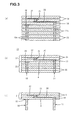
- Figs. 4 to 7 are views illustrating second to fifth embodiments of the present invention and each showing a portion corresponding to that of the multilayer electronic component 1 shown in Fig. 2 .
- the same reference numerals as in Fig. 2 designate constituent elements corresponding to those shown in Fig. 2 , and a duplicate description is omitted.
- the end surface 16 of the columnar conductor 10 is partly exposed in the recess portion 8.
- an area to which the solder 28 (see Fig. 2 ) is bondable can be decreased.
- the cross-sectional area of the columnar conductor 10 is increased so as to increase the mechanical strength thereof, the degree of freedom of surface wiring and the like at the mounting substrate 26 (see Fig. 2 ) side can be increased.
- the recess portion 8 is formed so as to have a larger cross-sectional area than that of the columnar conductor 10. Hence, the end surface 16 of the columnar conductor 10 is exposed at a part of the bottom surface of the recess portion 8. Hence, at the part of the bottom surface of the recess portion 8, the end surface 16 of the columnar conductor 10 is exposed. According to this embodiment, since the solder 28 (see Fig. 2 ) can be applied to a wider area, the bonding strength by soldering can be enhanced.
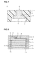
- the second end portion 14 of the columnar conductor 10 protrudes from the bottom surface of the recess portion 8.
- the solder 28 adheres onto a side surface 36 of the columnar conductor 10 besides the end surface 16 thereof, the bonding strength by soldering can be increased, and hence the reliability of electrical connection can be further improved.
- the cross-sectional area of the second end portion 14 of the columnar conductor 10 is set larger than that of the first end portion 12 (not shown in Fig. 7 ).
- the area of the end surface 16 can be increased, and thereby the area to which the solder 28 (see Fig. 2 ) adheres is increased; hence, as a result, the bonding strength by soldering can be increased, and in addition, the reliability of electrical connection can be further improved.
- the second end portion 14 of the columnar conductor 10 protrudes from the bottom surface of the recess portion 8
- the end surface 16 of the columnar conductor 10 may be formed at the same height as that of the bottom surface of the recess portion 8.
- the above columnar conductor 10 is formed to have a flange portion 37 at the second end portion 14.
- a laminate structure shown in Fig. 8 is employed instead of the laminate structure shown in Fig. 3(a) .
- the same reference numerals as in Fig. 3(a) designate the constituent elements corresponding to those shown in Fig. 3(a) , and a duplicate description is omitted.
- via conductors 10b and 11b which are to be formed into the columnar conductors 10 and 11, respectively, are formed larger in dimension in the radial direction than the via conductors 10a and 11a formed in other inorganic green sheets 35.
- the columnar conductor 10 having the flange portion 37 shown in Fig. 7 can be easily formed.
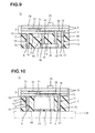
- Fig. 9 is a cross-sectional view showing a multilayer electronic component 1e of a sixth embodiment according to the present invention.
- the same reference numerals as in Fig. 1 designate constituent elements corresponding to those shown in Fig. 1 , and a duplicate description is omitted.
- a recess portion 41 is further provided, and an electronic element 42 such as a chip element is received in the recess portion 41.
- the electronic element 42 is located inside the recess portion 41 further from an opening face thereof.
- columnar conductors 43 and 44 are disposed in the resin layer 5, besides the columnar conductors 10 and 11, columnar conductors 43 and 44 are disposed.
- the columnar conductor 43 reaches the interface between the ceramic substrate 3 and the resin layer 5 and is integrated with a conductor film 45 formed on the one-side major surface 4 of the ceramic substrate 3.
- the columnar conductor 44 passes through the interface between the ceramic substrate 3 and the resin layer 5, extends inside of the ceramic substrate 3, and is then integrated with the conductor film 20.
- the other end portions of the columnar conductors 43 and 44 have end surfaces 46 and 47, respectively, which are each located inside the recess portion 41 further from the opening face thereof and exposed in the recess portion 41.
- the electronic element 42 which is electrically connected to the end surfaces 46 and 47 of the columnar conductors 43 and 44, respectively, is received in the recess portion 41.
- the multilayer electronic component 1e shown in Fig. 9 can be designed to advantageously form a high density mounting configuration.
- Fig. 10 is a cross-sectional view showing a multilayer electronic component 1f of a seventh embodiment according to the present invention.
- the same reference numerals as in Fig. 1 designate constituent elements corresponding to those shown in Fig. 1 , and a duplicate description is omitted.
- the dimension in the height direction of the electronic element 23 on the ceramic substrate 3 is larger than the dimension in the axis line direction of the columnar conductor 10 on the ceramic substrate 3.
- the dimensions of the columnar conductors 10 and 11 in the axis line direction are different from each other.
- the mechanical strength can be increased for the ceramic substrate 3, and the resistance against a lateral pushing force can also be increased.
- the resistance against a lateral pushing force is increased as described above, the cross-sectional dimension of the columnar conductor 10 can be decreased.
- the mounting substrate 26 is shown by an imaginary line.
- a pin-shaped connection portion 49 is provided as the conductive connection portion. This pin-shaped connection portion 49 is inserted into the recess portion 8 and is connected to the columnar conductor 10 by soldering, thereby forming the electrical connection.
Landscapes
- Engineering & Computer Science (AREA)
- Microelectronics & Electronic Packaging (AREA)
- Manufacturing & Machinery (AREA)
- Production Of Multi-Layered Print Wiring Board (AREA)
Abstract
Description
- The present invention relates to a multilayer electronic component, an electronic device comprising the multilayer electronic component, and a method for manufacturing a multilayer electronic component, and in particular, relates to a multilayer electronic component having a laminate structure in which a resin layer is formed on a ceramic substrate, an electronic device having the structure in which this multilayer electronic component is mounted on a mounting substrate, and a method for manufacturing a multilayer electronic component.
- As a multilayer electronic component which is of interest to the present invention, for example, there may be mentioned an electronic component which is integrally formed from a plurality of electronic elements, such as a semiconductor element and a chip element, and which has the structure in which electronic elements, such as a semiconductor element and a chip element, are mounted on a one-side major surface of a ceramic substrate, and in which the electronic elements are buried in a resin layer formed on the one-side major surface of the ceramic substrate (for example, see Patent Document 1).
- When a particular electronic device is formed using a multilayer electronic component having the structure as described above, the multilayer electronic component is mounted on a mounting substrate which is to be used as a mother board. The multilayer electronic component has pad electrodes for external connection, which are generally formed on an outside-facing major surface of a resin layer of the multilayer electronic component, and when the pad electrodes are connected to conductive lands formed on the mounting substrate by soldering, a mounting state is obtained. The above pad electrodes are electrically connected to respective wiring conductors provided at a ceramic substrate side via columnar conductors (via conductors) disposed in the resin layer.
- In addition, reduction in size and height has been always required of an electronic device having the multilayer electronic component as described above. As described above, when the structure in which the multilayer electronic component is mounted on the mounting substrate is carefully observed, even the thickness of a solder provided between the pad electrode at the multilayer electronic component side and the conductive land at the mounting substrate side interferes with the reduction in size and height, and when the reduction in size and height is further pursued, the reduction in thickness of the solder also becomes an important subject. Furthermore, it may also be construed that even the thickness of the pad electrode and that of the conductive land also interfere with the reduction in size and height.
Patent Document 1:Japanese Unexamined Patent Application Publication No. 2003-124435 - Accordingly, an object of the present invention is to provide a multilayer electronic component which can sufficiently meet the requirement for reduction in size and height described above and a method for manufacturing the multilayer electronic component.
- Another object of the present invention is to provide an electronic device configured to realize the reduction in size and height, which has the structure in which a multilayer electronic component is mounted on a mounting substrate.
- The present invention relates to a multilayer electronic component having a ceramic substrate and a resin layer formed on a major surface of the ceramic substrate, and the multilayer electronic component has the following structure in order to solve the technical problems described above.
- That is, at least one recess portion is disposed in the resin layer at an outside-facing major surface thereof. In addition, in the resin layer, at least one columnar conductor is disposed so that an axis line direction thereof is aligned in a thickness direction of the resin layer. A first end portion of this columnar conductor in the axis line direction reaches at least an interface between the ceramic substrate and the resin layer, and a second end portion of the columnar conductor opposite to the first end portion is located inside the recess portion further from an opening face thereof and has an end portion which is exposed in the recess portion.
- The columnar conductor is preferably formed from a sintered metal conductor integrated with a via conductor formed in the ceramic substrate.
- An end surface of the columnar conductor may be partly exposed in the recess portion, the second end portion of the columnar conductor may protrude from a bottom surface of the recess portion, or the second end portion of the columnar conductor may have a cross-sectional area larger than a cross-sectional area of the first end portion.
- The multilayer electronic component according to the present invention may further comprise a first electronic element which is mounted on the ceramic substrate and which is built in the resin layer. In the case described above, the dimension in a height direction of the first electronic element on the ceramic substrate may be greater than the dimension in the axis line direction of the columnar conductor on the ceramic substrate.
- The multilayer electronic component according to the present invention may further comprise a second electronic element which is received inside the recess portion described above. The second electronic element is located inside the recess portion further from the opening face thereof.
- The present invention relates to an electronic device comprising the multilayer electronic component as described above and a mounting substrate on which this multilayer electronic component is mounted. In the electronic device according to the present invention, the multilayer electronic component is disposed so that the major surface in which the recess portion is formed faces the mounting substrate, and the columnar conductor is electrically connected to a conductive connection portion formed on the mounting substrate via a conductive connection member provided inside the recess portion.
- In the electronic device according to the present invention, the conductive connection member preferably comprises a solder.
- In addition, the conductive connection portion protrudes from a surface of the mounting substrate by a predetermined height, and the conductive connection portion is preferably fitted inside the recess portion.
- The present invention also relates to a method for manufacturing a multilayer electronic component.
- The method for manufacturing a multilayer electronic component, according to the present invention, comprises: a composite-substrate-forming process for forming a composite substrate including a ceramic substrate, and a resin layer formed on a major surface of the ceramic substrate, wherein at least one columnar conductor is embedded in the resin layer so that an axis line direction of the columnar conductor is aligned in a thickness direction of the resin layer; and a recess-portion-forming process for forming at least one recess portion at an outside-facing major surface of the resin layer so as to expose at least an end surface of an end portion of the columnar conductor, the end portion being located at the outside-facing major surface of the resin layer.
- The composite-substrate-forming process described above is preferably performed as described below.
- A not-yet sintered composite laminate is first formed which includes a not-yet sintered ceramic molded body having a conductive portion formed at a predetermined position of a major surface of the not-yet sintered ceramic molded body and a non-sinterable inorganic material molded body which contains an inorganic material powder, which is not sintered at a sintering temperature of the ceramic molded body, and in which the columnar conductor is embedded so that the axis line direction thereof is aligned in a thickness direction of the non-sinterable inorganic material molded body, wherein the not-yet sintered ceramic molded body and the non-sinterable inorganic material molded body are laminated such that the conductive portion and an end portion of the columnar conductor is brought into contact with each other.
- Next, the not-yet sintered composite laminate is fired at a temperature at which the ceramic molded body is sintered and at which the inorganic material molded body is not sintered. Accordingly, the ceramic molded body is formed into the ceramic substrate.
- Next, the non-sinterable inorganic material molded body is removed from the fired composite laminate. As a result, the ceramic substrate provided with the columnar conductor protruding from a major surface of the ceramic substrate is obtained.
- Next, the resin layer is formed on the major surface of the ceramic substrate so as to bury the columnar conductor, and as a result, the above-described composite substrate is formed.
- In the preferable embodiment described above, the conductive portion provided at a predetermined position of the major surface of the not-yet sintered ceramic molded body is preferably formed from a via conductor to be formed in the ceramic substrate.
- In addition, in the preferable embodiment described above, in order to form the resin layer, the resin layer is preferably formed by transfer molding.
- In addition, before the step of forming the resin layer, a step of mounting an electronic element on the major surface of the ceramic substrate may be performed.
- In addition, in the method for manufacturing a multilayer electronic component, according to the present invention, the recess-portion-forming process may be performed by irradiating the outside-facing major surface of the resin layer with laser light.
- In addition, the resin layer may be made of a photosensitive resin. In this case, the recess-portion-forming process includes a step of exposing the photosensitive resin with a mask having an opening at an area other than an area at which the recess portion is to be formed and a step of performing development to form the recess portion.
- According to the multilayer electronic component of the present invention, since the end surface of the columnar conductor disposed inside the resin layer is located inside the recess portion further from the opening face thereof and is also exposed in the recess portion, when this multilayer electronic component is mounted on the mounting substrate, the conductive connection member, such as a solder, configured to electrically connect the columnar conductor to the conductive connection portion formed on the mounting substrate can be disposed inside the recess portion.
- Accordingly, regardless of the thickness of the conductive connection member, the reduction in size and height of the electronic device having the structure in which the multilayer electronic component is mounted on the mounting substrate can be realized. In addition, since the thickness of the conductive connection member can be increased without interfering with the reduction in size and height, the reliability of the electrical connection between the columnar conductor and the mounting substrate can be improved.
- In the multilayer electronic component according to the present invention, when the columnar conductor is formed from the sintered metal conductor integrated with the via conductor formed in the ceramic substrate, the reliability in electrical connection at the interface between the ceramic substrate and the resin layer can be improved, and in addition, the mechanical strength can also be increased. In addition, the columnar conductor can be made to have superior conductivity, heat dissipation properties, and solder bonding properties. In addition, in the structure described above, when the aspect ratio of the columnar conductor is high, a stress is concentrated on the columnar conductor at an interface portion between the ceramic substrate and the resin layer, and cracking is liable to occur; however, when the recess portion is provided in the resin layer, the aspect ratio can be decreased.
- When the end surface of the columnar conductor is partly exposed in the recess portion, while the mechanical strength of the columnar conductor is increased by increasing the cross-sectional area of the columnar conductor, the area of a bonding portion of the conductive connection member, such as a solder, which is used when the multilayer electronic component is mounted on the mounting substrate, can be decreased. As a result, the degree of freedom of surface wiring and the like of the mounting substrate can be increased.
- When the second end portion of the columnar conductor is exposed at the bottom surface of the recess portion, the conductive connection member provided when the multilayer electronic component is mounted on the mounting substrate adheres onto the side surface of the columnar conductor besides the end surface, and as a result, the strength of bonding obtained using the conductive connection member such as a solder can be increased.
- In the case in which the cross-sectional area of the second end portion of the columnar conductor is larger than that of the first end portion, when bonding, such as soldering, is performed using the conductive connection member, a bondable area of the columnar conductor to the conductive connection member such as a solder is increased, and as a result, the bonding strength by the conductive connection member can be increased.
- Since the multilayer electronic component according to the present invention has the columnar conductor which has the end surface exposed in the recess portion, when an electronic element is received in the recess portion to be electrically connected to the end surface of the columnar conductor, the structure can be obtained which is advantageous when the mounting density is improved.
- According to the electronic device of the present invention, since the columnar conductor and the conductive connection portion at the mounting substrate side are formed so as to be directly bonded to each other with the conductive connection member, a pad electrode or the like is not necessary to be provided with the multilayer electronic component, and as a result, the manufacturing process of the multilayer electronic component can be more simplified.
- When a solder is used as the above conductive connection member, since being provided in the recess portion, the solder is unlikely to flow out of the recess portion, and as a result, solder flash can be made unlikely to be generated.
- In the electronic device according to the present invention, when the conductive connection portion provided so as to protrude from the surface of the mounting substrate by a predetermined dimension in a height direction is fitted in the recess portion of the multilayer electronic component, the size and the height of the electronic device can be further reduced. In addition, since the dimension of the columnar conductor can be decreased in the axis line direction by a length corresponding to the dimension of the conductive connection portion in the height direction, strength against stress applied to the columnar conductor in a direction perpendicular to the axis line direction thereof, that is, resistance against a lateral pushing force, can be improved. Furthermore, when the conductive connection portion is fitted in the recess portion, alignment of the multilayer electronic component with respect to the mounting substrate can be performed.
- According to the method for manufacturing a multilayer electronic component of the present invention, after manufacturing the composite substrate in the state in which the columnar conductor is buried in mounting, since the recess portion is formed in the resin layer so as to expose at least the end surface of the columnar conductor, the dimension in the axis line direction and the position of the end surface of the columnar conductor of the composite substrate are not required to have a very high accuracy. Hence, process control for manufacturing the multilayer electronic component can be simplified.
- When the columnar conductor is formed from a sintered metal conductor, it is relatively difficult to obtain the dimension of the columnar conductor in the axis line direction with good repeatability due to, for example, influence of firing conditions and the like. Although there has been the problem as described above, according to the present invention, the end surface of the columnar conductor and the surface of the resin layer are not necessarily flush with each other, the columnar conductor may be simply formed so as to be buried in the resin layer, and the variation in dimension of the columnar conductor in the axis line direction may be adjusted by the depth of the recess portion.
- In addition, according to the method for manufacturing a multilayer electronic component of the present invention, since a method for milling the entire surface of the resin layer is not used in order to expose the end surface of the columnar conductor, the resin layer can be formed to have a uniform thickness; hence, the accuracy of the dimension in the height direction of the obtained multilayer electronic component can be improved.
- In the method for manufacturing a multilayer electronic component according to the present invention, when the process for forming the composite substrate is used, as described above, having a step of forming a not-yet sintered composite laminate which includes a not-yet sintered ceramic molded body and a non-sinterable inorganic material molded body in which the columnar conductor is buried; a step of firing the not-yet sintered composite laminate at a temperature at which the ceramic molded body is sintered and at which the inorganic material molded body is not sintered; and a step of removing the non-sinterable inorganic material molded body from the fired composite laminate, the ceramic substrate provided with the columnar conductor protruding from a major surface thereof can be easily obtained. Subsequently, when the resin layer is formed on the major surface of the ceramic substrate so as to bury the columnar conductor, the composite substrate can be efficiency obtained.
- When the via conductor is formed in the ceramic molded body forming the above not-yet sintered composite laminate, and when the end portion of the columnar conductor is formed so as to be brought into contact with this via conductor, the structure can be easily obtained in which the columnar conductor is formed from the sintered metal conductor integrated with the via conductor formed in the ceramic substrate.
- When transfer molding is used for forming the resin layer of the composite substrate, by using a mold having a flat surface which is brought into contact with the surface of the resin layer, the surface of the resin layer can be easily formed so as to have excellent flatness. In addition, as described above, when the columnar conductor is formed from a sintered metal conductor, it is relatively difficult to obtain the dimension of the columnar conductor in the axis line direction with superior repeatability due to, for example, the influence of firing conditions; however, according to the present invention, the resin layer may be simply formed so as to bury the columnar conductor therein, and hence molding using transfer molding can be applied to the formation of the resin layer without causing any problems.
- In the method for manufacturing a multilayer electronic component, according to the present invention, in order to form the recess portion in the resin layer, when irradiation of laser light is performed, or when exposure and development of a photosensitive resin are performed, a desired recess portion having high accuracy in terms of dimension, shape, and position can be easily formed.
-
-
Fig. 1 is a cross-sectional view showing a multilayerelectronic component 1 of a first embodiment according to the present invention. -
Fig. 2 is a partly enlarged cross-sectional view showing anelectronic device 2 formed by mounting the multilayerelectronic component 1 shown inFig. 1 on a mountingsubstrate 26. -
Fig. 3 includes views illustrating a method for manufacturing the multilayerelectronic component 1 shown inFig. 1 , and in particular, for illustrating steps of manufacturing a composite substrate. -
Fig. 4 is a partly enlarged cross-sectional view showing a multilayer electronic component 1a of a second embodiment according to the present invention. -
Fig. 5 is a partly enlarged cross-sectional view showing a multilayerelectronic component 1b of a third embodiment according to the present invention. -
Fig. 6 is a partly enlarged cross-sectional view showing a multilayer electronic component 1c of a fourth embodiment according to the present invention. -
Fig. 7 is a partly enlarged cross-sectional view showing a multilayer electronic component 1d of a fifth embodiment according to the present invention. -
Fig. 8 is a view illustrating a method for manufacturing the multilayer electronic component 1d shown inFig. 7 , the view being corresponding toFig. 3(a) . -
Fig. 9 is a cross-sectional view showing a multilayer electronic component 1e of a sixth embodiment according to the present invention. -
Fig. 10 is a cross-sectional view showing a multilayer electronic component 1f of a seventh embodiment according to the present invention. -
- 1, 1a, 1b, 1c, 1d, 1e, 1f
- multilayer electronic component
- 2
- electronic device
- 3
- ceramic substrate
- 4, 7, 24
- major surface
- 5
- resin layer
- 8, 9, 41
- recess portion
- 10, 11, 43, 44
- columnar conductor
- 12, 13
- first end portion
- 14, 15
- second end portion
- 16, 17, 46, 47
- end surface
- 18, 20, 22, 45
- conductor film
- 19, 21
- via conductor
- 23, 25, 42
- electronic element
- 26
- mounting substrate
- 27
- conductor land
- 28
- solder
- 31
- composite laminate
- 32
- ceramic molded body
- 33
- inorganic material molded body
-
Figs. 1 to Fig. 3 are views illustrating a first embodiment according to the present invention. In this embodiment,Fig. 1 is a cross-sectional view of a multilayerelectronic component 1,Fig. 2 is a partly enlarged cross-sectional view of anelectronic device 2 obtained by mounting the multilayerelectronic component 1 shown inFig. 1 on a mounting substrate, andFig. 3 includes cross-sectional views illustrating a method for manufacturing the multilayerelectronic component 1. - As shown in
Fig. 1 , the multilayerelectronic component 1 has aceramic substrate 3 and aresin layer 5 formed on a one-side major surface 4 of theceramic substrate 3. Theceramic substrate 3 has a multilayer structure formed ofceramic layers 6 laminated to each other. Theceramic layer 6 is formed, for example, from a low-temperature firing ceramic material containing Al2O3 as filler and borosilicate glass as a sintering additive. In addition, theresin layer 5 is formed, for example, of an epoxy-based resin. The plan dimension of theceramic substrate 3 is set, for example, to 105 mm by 105 mm. - At an outside-facing
major surface 7 side of theresin layer 5,recess portions resin layer 5,columnar electrodes resin layer 5. Thecolumnar conductors -
First end portions columnar conductors ceramic substrate 3 and theresin layer 5, that is, the one-side major surface 4 of theceramic substrate 3. In addition,second end portions columnar conductors first end portions recess portions end surfaces recess portions - More particularly, the
first end portion 12 of thecolumnar conductor 10 is located on the one-side major surface 4 of theceramic substrate 3 and is integrated with aconductor film 18 formed on this major surface 4. Thefirst end portion 13 of the othercolumnar conductor 11 is located inside theceramic substrate 3 and is integrated with aconductor film 20 formed along the interface between theceramic layers 6 and with a viaconductor 19 penetrating theceramic layer 6 in the thickness direction. According to the structure as described above, thecolumnar conductor 11 may have a high mechanical strength, in particular, the resistance against a lateral pushing force, as compared to that of thecolumnar conductor 10. In this embodiment, thecolumnar conductors - In
Fig. 1 , as constituent elements formed inside theceramic substrate 3, besides the viaconductor 19 and theconductor film 20, a viaconductor 21 and aconductor film 22 are also shown. - The above
columnar conductors conductor films conductors columnar conductors - The cross-section of the
columnar conductors recess portions columnar conductors recess portions - In addition, as one example, the dimensions of the
columnar conductors ceramic substrate 3 are each set to 0.7 mm, and in addition, the thickness of theresin layer 5 is set to 0.8 mm. Accordingly, the depths of therecess portions recess portions - In addition, the multilayer
electronic component 1 has anelectronic element 23 mounted on the one-side major surface 4 of theceramic substrate 3 and embedded in theresin layer 5. Theelectronic element 23 is a semiconductor element such as an 1C chip. Anelectronic element 25 is mounted on the othermajor surface 24 of theceramic substrate 3. Theelectronic element 25 is a chip element such as a multilayer ceramic capacitor. - In
Fig. 1 , a mountingsubstrate 26 is shown by an imaginary line. When theelectronic device 2 as shown inFig. 2 is formed, the multilayerelectronic component 1 is mounted on the mountingsubstrate 26. In this step, the multilayerelectronic component 1 is placed so that themajor surface 7 in which theabove recess portions substrate 26 side. - In
Fig. 2 , thecolumnar conductor 10, which is one of the columnar conductors shown inFig. 1 , and the structure relating thereto are shown. The othercolumnar conductor 11 and the structure relating thereto are substantially the same as those of thecolumnar conductor 10 show inFig. 2 , and hence the figure and description of thecolumnar conductor 11 are omitted. - As shown in
Fig. 2 , aconductive land 27 used as a conductive connection portion is formed on the mountingsubstrate 26. The mountingsubstrate 26 is formed, for example, from a printed circuit board, and theconductive land 27 is formed, for example, from a Cu foil having a thickness of 100 µm. Thecolumnar conductor 10 is electrically connected to theconductive land 27 via asolder 28 provided in therecess portion 8. In particular, in this embodiment, a constituent element such as a pad electrode is not provided at the multilayerelectronic component 1 side, and thecolumnar conductor 10 and theconductive land 27 are directly connected to each other with thesolder 28 provided therebetween. - As apparent from
Fig. 2 , since thesolder 28 is provided inside therecess portion 8, the thickness of thesolder 28 does not interfere with the reduction in size and height of theelectronic device 2. In addition, even when thesolder 28 is sufficiently provided in order to enhance the reliability in electrical connection between thecolumnar conductor 10 and theconductive land 27, it is possible to make thesolder 28 unlikely to flow out of therecess portion 8, and hence the generation of solder flash can be suppressed. In addition, since theconductive land 27 is fitted in therecess portion 8, the thickness of theconductive land 27 does not interfere with the reduction in size and height of theelectronic device 2. In addition, the alignment of the multilayerelectronic component 1 with respect to the mountingsubstrate 26 is easily performed, and in addition, the resistance against a lateral pushing force can be increased. From the above point of view, the thickness of theconductive land 27 is preferably set to 5 µm or more. In addition, in this embodiment, although theconductive land 27 is fitted in therecess portion 8, the conductive connection portion is not limited to theconductive land 27, and for example, a wiring conductor, which is not fitted in therecess portion 8 and is exposed only on the surface of the mountingsubstrate 26, may also be used. - The multilayer
electronic component 1 shown inFig. 1 is manufactured as described below. - That is, in order to manufacture the multilayer
electronic component 1, a composite-substrate-forming process for forming a composite substrate, which has theceramic substrate 3 and theresin layer 5 burying thecolumnar conductors recess portions resin layer 5 at the outside-facingmajor surface 7 side so as to expose at least the end surfaces 16 and 17 of thesecond end portions columnar conductors -
Fig. 3 includes views illustrating the composite-substrate-forming process. InFig. 3 , the same reference numerals as inFig. 1 designate constituent elements corresponding to those inFig. 1 , and a duplicate description is omitted. - In order to form the composite substrate, a not-yet sintered
composite laminate 31 as shown inFig. 3(b) is formed. The not-yet sinteredcomposite laminate 31 has a not-yet sintered ceramic moldedbody 32 and a non-sinterable inorganic material molded body 33. The ceramic moldedbody 32 is to be formed into theceramic substrate 3, and in this ceramic moldedbody 32, the above-describedconductor films conductors body 32, conductive portions are formed by theconductor film 18 and the viaconductor 19. - The non-sinterable inorganic material molded body 33 contains an inorganic material powder that is not sintered at a sintering temperature of the ceramic molded
body 32. As described above, when theceramic layer 6, by which the ceramic moldedbody 32 is to be formed, is formed using a ceramic material which contains Al2O3 as filler and borosilicate glass as a sintering additive, Al2O3 powder is advantageously used as the inorganic material powder contained in the inorganic material molded body 33. In the inorganic material molded body 33, thecolumnar conductors columnar conductors columnar conductors conductor film 18 and the viaconductor 19. Furthermore, the same composition is preferably used. Accordingly, the bonding forces between the conductive portions and the respectivecolumnar conductors columnar conductors ceramic substrate 3 and theresin layer 5 can be further improved. - In addition, in the
composite laminate 31, the not-yet sintered ceramic moldedbody 32 and the non-sinterable inorganic material molded body 33 are laminated to each other so that theconductor film 18 and the viaconductor 19 functioning as the conductive portions are brought into contact with the end portions of thecolumnar conductors - In order to form the above not-yet sintered
composite laminate 31, a plurality of ceramicgreen sheets 34 to be formed into the ceramic moldedbody 32 and a plurality of inorganic materialgreen sheets 35 to be formed into the inorganic material molded body 33 are prepared as shown inFig. 3(a) . - On specific ceramic
green sheets 34, theconductive films green sheets 34, the viaconductors - In addition, in each of the inorganic material
green sheets 35, viaconductors columnar conductors - In order to form the not-yet sintered
composite laminate 31, shown inFig. 3(b) , the ceramicgreen sheets 34 and the inorganic materialgreen sheets 35, which are shown inFig. 3(a) , may be laminated sheet by sheet starting form the sheet located at a one-end side in the lamination direction, or after the ceramicgreen sheets 34 are laminated to form the ceramic moldedbody 32, and the inorganic materialgreen sheets 35 are laminated to form the inorganic material molded body 33, the ceramic moldedbody 32 and the inorganic material molded body 33 may be laminated to each other. - Next, the not-yet sintered
composite laminate 31 is fired at a temperature, such as 870°C, at which the ceramic moldedbody 32 is sintered but the inorganic material molded body 33 is not sintered. As a result, the ceramic moldedbody 32 is formed into the sinteredceramic substrate 3. On the other hand, the inorganic material molded body 33 still remains in a non-sintered state. - Next, the non-sinterable inorganic material molded body 33 is removed from the fired
composite laminate 31. Even after the firing, the inorganic material molded body 33 is still in a non-sintered state, the removal thereof can be easily performed. By the removal of the inorganic material molded body 33, as shown inFig. 3(c) , theceramic substrate 3 provided with thecolumnar conductors ceramic substrate 3 can be obtained. - Next, whenever necessary, after the electronic element 23 (see
Fig. 1 ) is mounted on the one-side major surface 4 of theceramic substrate 3, theresin layer 5 is formed on the one-side major surface 4 of theceramic substrate 3 so as to bury thecolumnar conductors recess portions electronic component 1 shown inFig. 1 is formed. - For the formation of the
resin layer 5 described above, molding is preferably performed by transfer molding. By the transfer molding, since the surface of theresin layer 5 is formed in conformity with the shape of a mold, the surface can be easily planarized. However, when the above advantage is not desired, a dispenser method may be used for forming theresin layer 5. - Next, a process for forming the
recess portions major surface 7 of theresin layer 5 with laser light. Parts of theresin layer 5 covering thecolumnar conductors columnar conductors columnar conductors recess portions recess portions columnar conductors recess portions recess portions - The
resin layer 5 may be formed using a photosensitive resin. In this case, in order to form therecess portions recess portions recess portions - The
resin layer 5 is formed so as to bury thecolumnar conductors recess portions resin layer 5 so as to expose the end surfaces 16 and 17 of thecolumnar conductors columnar conductors resin layer 5 by the variation can be substantially avoided. In addition, by adjusting the depths of therecess portions columnar conductors columnar conductors - The
columnar conductors columnar conductors conductor film 18 and the via conductor 19) formed at predetermined portions of the one-side major surface 4 of theceramic substrate 3, followed by heat curing. - Next, whenever necessary, the
electronic component 25 is mounted on the outside-facingmajor surface 24 of theceramic substrate 3. - By the processes described above, the multilayer
electronic component 1 shown inFig. 1 is obtained. -
Figs. 4 to 7 are views illustrating second to fifth embodiments of the present invention and each showing a portion corresponding to that of the multilayerelectronic component 1 shown inFig. 2 . InFigs. 4 to 7 , the same reference numerals as inFig. 2 designate constituent elements corresponding to those shown inFig. 2 , and a duplicate description is omitted. - In a multilayer electronic component 1a shown in
Fig. 4 , theend surface 16 of thecolumnar conductor 10 is partly exposed in therecess portion 8. According to this embodiment, compared to the cross-sectional area of thecolumnar conductor 10, that is, the area of theend surface 16, an area to which the solder 28 (seeFig. 2 ) is bondable can be decreased. Hence, while the cross-sectional area of thecolumnar conductor 10 is increased so as to increase the mechanical strength thereof, the degree of freedom of surface wiring and the like at the mounting substrate 26 (seeFig. 2 ) side can be increased. - In a multilayer
electronic component 1b shown inFig. 5 , therecess portion 8 is formed so as to have a larger cross-sectional area than that of thecolumnar conductor 10. Hence, theend surface 16 of thecolumnar conductor 10 is exposed at a part of the bottom surface of therecess portion 8. Hence, at the part of the bottom surface of therecess portion 8, theend surface 16 of thecolumnar conductor 10 is exposed. According to this embodiment, since the solder 28 (seeFig. 2 ) can be applied to a wider area, the bonding strength by soldering can be enhanced. - In a multilayer electronic component 1c shown in
Fig. 6 , thesecond end portion 14 of thecolumnar conductor 10 protrudes from the bottom surface of therecess portion 8. According to this embodiment, since the solder 28 (seeFig. 2 ) adheres onto aside surface 36 of thecolumnar conductor 10 besides theend surface 16 thereof, the bonding strength by soldering can be increased, and hence the reliability of electrical connection can be further improved. - In a multilayer electronic component 1d shown in
Fig. 7 , the cross-sectional area of thesecond end portion 14 of thecolumnar conductor 10 is set larger than that of the first end portion 12 (not shown inFig. 7 ). According to this embodiment, the area of theend surface 16 can be increased, and thereby the area to which the solder 28 (seeFig. 2 ) adheres is increased; hence, as a result, the bonding strength by soldering can be increased, and in addition, the reliability of electrical connection can be further improved. InFig. 7 , although thesecond end portion 14 of thecolumnar conductor 10 protrudes from the bottom surface of therecess portion 8, theend surface 16 of thecolumnar conductor 10 may be formed at the same height as that of the bottom surface of therecess portion 8. - In order to increase the cross-sectional area of the
second end portion 14, theabove columnar conductor 10 is formed to have aflange portion 37 at thesecond end portion 14. In order to obtain thecolumnar conductor 10 having the structure as described above, instead of the laminate structure shown inFig. 3(a) , a laminate structure shown inFig. 8 is employed. InFig. 8 , the same reference numerals as inFig. 3(a) designate the constituent elements corresponding to those shown inFig. 3(a) , and a duplicate description is omitted. - As shown in
Fig. 8 , in an inorganic materialgreen sheet 35a disposed at an end portion in the laminate direction, viaconductors columnar conductors conductors green sheets 35. By the laminate structure as described above, thecolumnar conductor 10 having theflange portion 37 shown inFig. 7 can be easily formed. In addition, whenever necessary, there may be formed at least two inorganic materialgreen sheets 35a provided with the viaconductors -
Fig. 9 is a cross-sectional view showing a multilayer electronic component 1e of a sixth embodiment according to the present invention. InFig. 9 , the same reference numerals as inFig. 1 designate constituent elements corresponding to those shown inFig. 1 , and a duplicate description is omitted. - In the multilayer electronic component 1e shown in
Fig. 9 , besides therecess portions recess portion 41 is further provided, and anelectronic element 42 such as a chip element is received in therecess portion 41. Theelectronic element 42 is located inside therecess portion 41 further from an opening face thereof. - In addition, in the
resin layer 5, besides thecolumnar conductors columnar conductors columnar conductor 43 reaches the interface between theceramic substrate 3 and theresin layer 5 and is integrated with aconductor film 45 formed on the one-side major surface 4 of theceramic substrate 3. In addition, thecolumnar conductor 44 passes through the interface between theceramic substrate 3 and theresin layer 5, extends inside of theceramic substrate 3, and is then integrated with theconductor film 20. - In addition, the other end portions of the
columnar conductors end surfaces recess portion 41 further from the opening face thereof and exposed in therecess portion 41. Theelectronic element 42 which is electrically connected to the end surfaces 46 and 47 of thecolumnar conductors recess portion 41. - The multilayer electronic component 1e shown in
Fig. 9 can be designed to advantageously form a high density mounting configuration. -
Fig. 10 is a cross-sectional view showing a multilayer electronic component 1f of a seventh embodiment according to the present invention. InFig. 10 , the same reference numerals as inFig. 1 designate constituent elements corresponding to those shown inFig. 1 , and a duplicate description is omitted. - In the multilayer electronic component 1f shown in
Fig. 10 , in particular, the dimension in the height direction of theelectronic element 23 on theceramic substrate 3 is larger than the dimension in the axis line direction of thecolumnar conductor 10 on theceramic substrate 3. In addition, the dimensions of thecolumnar conductors - As is the case of the
columnar conductor 10, when the dimension in the axis line direction is decreased, the mechanical strength can be increased for theceramic substrate 3, and the resistance against a lateral pushing force can also be increased. In addition, when the resistance against a lateral pushing force is increased as described above, the cross-sectional dimension of thecolumnar conductor 10 can be decreased. - In
Fig. 10 , the mountingsubstrate 26 is shown by an imaginary line. On the mountingsubstrate 26, a pin-shapedconnection portion 49 is provided as the conductive connection portion. This pin-shapedconnection portion 49 is inserted into therecess portion 8 and is connected to thecolumnar conductor 10 by soldering, thereby forming the electrical connection.
Claims (18)
- A multilayer electronic component comprising:a ceramic substrate; and a resin layer formed on a major surface of the ceramic substrate,wherein at least one recess portion is disposed in the resin layer at an outside-facing major surface thereof,at least one columnar conductor is disposed in the resin layer so that an axis line direction of the columnar conductor is aligned in a thickness direction of the resin layer, a first end portion of the columnar conductor in the axis line direction reaches at least an interface between the ceramic substrate and the resin layer, and a second end portion of the columnar conductor opposite to the first end portion is located inside the recess portion further from an opening face thereof and has an end surface which is exposed in the recess portion.
- The multilayer electronic component according to Claim 1, wherein the columnar conductor is formed from a sintered metal conductor which is integrated with a via conductor formed in the ceramic substrate.
- The multilayer electronic component according to Claim 1, wherein the end surface of the columnar conductor is partly exposed in the recess portion.
- The multilayer electronic component according to Claim 1, wherein the second end portion of the columnar conductor protrudes from a bottom surface of the recess portion.
- The multilayer electronic component according to Claim 1, wherein the second end portion of the columnar conductor has a cross-sectional area larger than a cross-sectional area of the first end portion.
- The multilayer electronic component according to Claim 1, further comprising a first electronic element which is mounted on the ceramic substrate and which is built in the resin layer.
- The multilayer electronic component according to Claim 6, wherein the dimension in a height direction of the first electronic element on the ceramic substrate is greater than the dimension in the axis line direction of the columnar conductor on the ceramic substrate.
- The multilayer electronic component according to Claim 1, further comprising a second electronic element which is received inside the recess portion, wherein the second electronic element is located inside the recess portion further from the opening face thereof.
- An electronic device comprising:the multilayer electronic component according to one of Claims 1 to 8; anda mounting substrate on which the multilayer electronic component is mounted,wherein the multilayer electronic component is disposed so that the major surface in which the recess portion is formed faces the mounting substrate; andthe columnar conductor is electrically connected to a conductive connection portion formed on the mounting substrate via a conductive connection member provided inside the recess portion.
- The electronic device according to Claim 9, wherein the conductive connection member comprises a solder.
- The electronic device according to Claim 9, wherein the conductive connection portion protrudes from a surface of the mounting substrate by a predetermined height and is fitted inside the recess portion.
- A method for manufacturing a multilayer electronic component, comprising:a composite-substrate-forming process for forming a composite substrate including a ceramic substrate, and a resin layer formed on a major surface of the ceramic substrate, wherein at least one columnar conductor is embedded in the resin layer so that an axis line direction of the columnar conductor is aligned in a thickness direction of the resin layer; anda recess-portion-forming process for forming at least one recess portion in the resin layer at an outside-facing major surface thereof so as to expose at least an end surface of an end portion of the columnar conductor, the end portion being located at the outside-facing major surface of the resin layer.
- The method for manufacturing a multilayer electronic component, according to Claim 12,
wherein the composite-substrate-forming process comprises:a step of forming a not-yet sintered composite laminate which includes a not-yet sintered ceramic molded body having a conductive portion formed at a predetermined position of a major surface thereof and a non-sinterable inorganic material molded body which contains an inorganic material powder, which is not sintered at a sintering temperature of the ceramic molded body, and in which the columnar conductor is embedded so that the axis line direction thereof is aligned in a thickness direction of the non-sinterable inorganic material molded body, wherein the not-yet sintered ceramic molded body and the non-sinterable inorganic material molded body are laminated such that the conductive portion and an end portion of the columnar conductor are brought into contact with each other;a step of firing the not-yet sintered composite laminate at a temperature at which the ceramic molded body is sintered and at which the inorganic material molded body is not sintered such that the ceramic molded body is formed into the ceramic substrate;a step of removing the non-sinterable inorganic material molded body from the fired composite laminate so as to recover the ceramic substrate provided with the columnar conductor protruding from a major surface thereof; anda step of forming the resin layer on the major surface of the ceramic substrate so as to bury the columnar conductor. - The method for manufacturing a multilayer electronic component, according to Claim 13, wherein the conductive portion formed at the predetermined position of the major surface of the not-yet sintered ceramic molded body is formed from a via conductor to be formed in the ceramic substrate.
- The method for manufacturing a multilayer electronic component, according to Claim 13, wherein the step of forming the resin layer includes a step of forming the resin layer by transfer molding.
- The method for manufacturing a multilayer electronic component, according to Claim 13, further comprising, before the step of forming the resin layer, a step of mounting an electronic element on the major surface of the ceramic substrate.
- The method for manufacturing a multilayer electronic component, according to Claim 12, wherein the recess-portion-forming process includes a step of irradiating the outside-facing major surface of the resin layer with laser light.
- The method for manufacturing a multilayer electronic component, according to Claim 12, wherein the resin layer is made of a photosensitive resin, and the recess-portion-forming process includes a step of exposing the photosensitive resin with a mask having an opening at an area other than an area at which the recess portion is to be formed and a step of performing development to form the recess portion.
Applications Claiming Priority (2)
| Application Number | Priority Date | Filing Date | Title |
|---|---|---|---|
| JP2005217376 | 2005-07-27 | ||
| PCT/JP2006/312300 WO2007013239A1 (en) | 2005-07-27 | 2006-06-20 | Stacked electronic component, electronic device and method for manufacturing stacked electronic component |
Publications (2)
| Publication Number | Publication Date |
|---|---|
| EP1909322A1 true EP1909322A1 (en) | 2008-04-09 |
| EP1909322A4 EP1909322A4 (en) | 2011-08-03 |
Family
ID=37683143
Family Applications (1)
| Application Number | Title | Priority Date | Filing Date |
|---|---|---|---|
| EP06766961A Withdrawn EP1909322A4 (en) | 2005-07-27 | 2006-06-20 | STACKED ELECTRONIC COMPONENT, ELECTRONIC DEVICE, AND METHOD FOR MANUFACTURING STACKED ELECTRONIC COMPONENT |
Country Status (4)
| Country | Link |
|---|---|
| US (1) | US7463475B2 (en) |
| EP (1) | EP1909322A4 (en) |
| JP (1) | JP4501936B2 (en) |
| WO (1) | WO2007013239A1 (en) |
Families Citing this family (10)
| Publication number | Priority date | Publication date | Assignee | Title |
|---|---|---|---|---|
| JP5600247B2 (en) * | 2008-06-11 | 2014-10-01 | 株式会社村田製作所 | Multilayer electronic component and manufacturing method thereof |
| US8618674B2 (en) * | 2008-09-25 | 2013-12-31 | Infineon Technologies Ag | Semiconductor device including a sintered insulation material |
| KR101032343B1 (en) * | 2009-05-12 | 2011-05-09 | 삼화콘덴서공업주식회사 | High Voltage MLC and DC-Link Capacitor Modules Using the Same |
| KR20130051614A (en) * | 2011-11-10 | 2013-05-21 | 삼성전기주식회사 | Multilayered ceramic electronic component and manufacturing method thereof |
| JP5862584B2 (en) * | 2013-03-08 | 2016-02-16 | 株式会社村田製作所 | Module, method for manufacturing the module, and electronic device including the module |
| KR102472945B1 (en) * | 2015-04-23 | 2022-12-01 | 삼성전기주식회사 | Printed circuit board, semiconductor package and method of manufacturing the same |
| CN107615894B (en) * | 2015-06-03 | 2020-07-17 | 株式会社村田制作所 | Component mounting board |
| JPWO2018186049A1 (en) * | 2017-04-06 | 2019-11-14 | 株式会社村田製作所 | Composite multilayer board |
| CN110199579B (en) * | 2017-09-14 | 2022-07-01 | 新电元工业株式会社 | Electronic module and method for manufacturing electronic module |
| US11850416B2 (en) * | 2018-06-22 | 2023-12-26 | The Regents Of The University Of Michigan | Method of manufacturing a probe array |
Family Cites Families (18)
| Publication number | Priority date | Publication date | Assignee | Title |
|---|---|---|---|---|
| JPS6094794A (en) | 1983-10-28 | 1985-05-27 | 株式会社日立製作所 | multilayer wiring board |
| JPH06120672A (en) | 1992-10-01 | 1994-04-28 | Hitachi Chem Co Ltd | Multilayer printed wiring board |
| JP3320932B2 (en) * | 1993-12-13 | 2002-09-03 | 松下電器産業株式会社 | Chip package mount, circuit board on which chip package is mounted, and method of forming circuit board |
| JP3188086B2 (en) * | 1993-12-29 | 2001-07-16 | 松下電器産業株式会社 | Ceramic wiring board, its manufacturing method and its mounting structure |
| JPH0983141A (en) | 1995-09-08 | 1997-03-28 | Matsushita Electric Ind Co Ltd | Manufacturing method of ceramic multilayer substrate |
| JP2943788B2 (en) | 1997-04-10 | 1999-08-30 | 日立エーアイシー株式会社 | Wiring board for mounting electronic components |
| JP3413348B2 (en) * | 1997-06-30 | 2003-06-03 | 太陽誘電株式会社 | Multilayer LC composite parts |
| US6462931B1 (en) * | 1997-10-23 | 2002-10-08 | Texas Instruments Incorporated | High-dielectric constant capacitor and memory |
| JP2000299560A (en) * | 1999-04-15 | 2000-10-24 | Matsushita Electric Ind Co Ltd | Manufacturing method of ceramic circuit board |
| US6528145B1 (en) * | 2000-06-29 | 2003-03-04 | International Business Machines Corporation | Polymer and ceramic composite electronic substrates |
| US6577490B2 (en) * | 2000-12-12 | 2003-06-10 | Ngk Spark Plug Co., Ltd. | Wiring board |
| JP2002261120A (en) * | 2001-03-06 | 2002-09-13 | Sony Corp | Mounting substrate, method of manufacturing the same, and semiconductor device |
| JP4868196B2 (en) | 2001-06-27 | 2012-02-01 | 株式会社村田製作所 | Manufacturing method of ceramic multilayer substrate |
| JP3890947B2 (en) * | 2001-10-17 | 2007-03-07 | 松下電器産業株式会社 | High frequency semiconductor device |
| US6711029B2 (en) * | 2002-05-21 | 2004-03-23 | Cts Corporation | Low temperature co-fired ceramic with improved shrinkage control |
| US6606237B1 (en) * | 2002-06-27 | 2003-08-12 | Murata Manufacturing Co., Ltd. | Multilayer capacitor, wiring board, decoupling circuit, and high frequency circuit incorporating the same |
| JP3988651B2 (en) * | 2003-01-31 | 2007-10-10 | 株式会社村田製作所 | Multilayer capacitors, wiring boards, decoupling circuits, and high-frequency circuits |
| US7095602B1 (en) * | 2005-06-29 | 2006-08-22 | Murata Manufacturing Co., Ltd. | Ceramic structure and nonreciprocal circuit device |
-
2006
- 2006-06-20 EP EP06766961A patent/EP1909322A4/en not_active Withdrawn
- 2006-06-20 JP JP2006539167A patent/JP4501936B2/en active Active
- 2006-06-20 WO PCT/JP2006/312300 patent/WO2007013239A1/en not_active Ceased
-
2007
- 2007-04-30 US US11/741,857 patent/US7463475B2/en active Active
Also Published As
| Publication number | Publication date |
|---|---|
| WO2007013239A1 (en) | 2007-02-01 |
| JPWO2007013239A1 (en) | 2009-02-05 |
| JP4501936B2 (en) | 2010-07-14 |
| EP1909322A4 (en) | 2011-08-03 |
| US20070267218A1 (en) | 2007-11-22 |
| US7463475B2 (en) | 2008-12-09 |
Similar Documents
| Publication | Publication Date | Title |
|---|---|---|
| US7463475B2 (en) | Multilayer electronic component, electronic device, and method for manufacturing multilayer electronic component | |
| CN101170878B (en) | Method for manufacturing print circuit board | |
| CN100568489C (en) | Circuit module and manufacturing method thereof | |
| CN101543152A (en) | Method for manufacturing substrate with built-in component and substrate with built-in component | |
| JP2006210524A (en) | Multilayer circuit board and manufacturing method thereof | |
| CN101303981A (en) | Wiring board with built-in components and method for manufacturing same | |
| JP2007201254A (en) | Semiconductor element built-in substrate, semiconductor element built-in type multilayer circuit board | |
| WO2014125973A1 (en) | Resin multi-layer substrate with built-in component, and resin multi-layer substrate | |
| KR100857165B1 (en) | Circuit Board Manufacturing Method | |
| CN105376926A (en) | Printed circuit board and manufacturing method thereof | |
| WO2005071744A1 (en) | Multilayer electronic part and structure for mounting multilayer electronic part | |
| JP5192865B2 (en) | Manufacturing method of wiring board with built-in components | |
| KR100861620B1 (en) | Manufacturing method of printed circuit board | |
| JP2009049444A (en) | Multilayer circuit board manufacturing method | |
| KR100757910B1 (en) | A buried pattern board and its manufacturing method | |
| JP4598140B2 (en) | Component built-in wiring board, method of manufacturing component built-in wiring board | |
| JP4443349B2 (en) | Manufacturing method of multilayer wiring board | |
| JP4385782B2 (en) | Composite multilayer substrate and manufacturing method thereof | |
| JP5192864B2 (en) | Manufacturing method of wiring board with built-in components | |
| JP2006186058A (en) | Component built-in module and manufacturing method thereof | |
| JP2014049509A (en) | Wiring board manufacturing method | |
| CN108464061A (en) | The manufacturing method of including components therein substrate and including components therein substrate | |
| KR100565501B1 (en) | Passive element embedded circuit board and its manufacturing method | |
| JP2007317712A (en) | Component built-in composite wiring board and manufacturing method thereof | |
| KR101005491B1 (en) | Electronic device mounted printed circuit board and printed circuit board manufacturing method |
Legal Events
| Date | Code | Title | Description |
|---|---|---|---|
| PUAI | Public reference made under article 153(3) epc to a published international application that has entered the european phase |
Free format text: ORIGINAL CODE: 0009012 |
|
| 17P | Request for examination filed |
Effective date: 20070426 |
|
| AK | Designated contracting states |
Kind code of ref document: A1 Designated state(s): AT BE BG CH CY CZ DE DK EE ES FI FR GB GR HU IE IS IT LI LT LU LV MC NL PL PT RO SE SI SK TR |
|
| A4 | Supplementary search report drawn up and despatched |
Effective date: 20110705 |
|
| RIC1 | Information provided on ipc code assigned before grant |
Ipc: H01L 23/12 20060101AFI20110629BHEP Ipc: H01L 25/00 20060101ALI20110629BHEP |
|
| DAX | Request for extension of the european patent (deleted) | ||
| STAA | Information on the status of an ep patent application or granted ep patent |
Free format text: STATUS: THE APPLICATION IS DEEMED TO BE WITHDRAWN |
|
| 18D | Application deemed to be withdrawn |
Effective date: 20160105 |