EP1909175B1 - Memory management method and portable terminal device - Google Patents
Memory management method and portable terminal device Download PDFInfo
- Publication number
- EP1909175B1 EP1909175B1 EP07252969.6A EP07252969A EP1909175B1 EP 1909175 B1 EP1909175 B1 EP 1909175B1 EP 07252969 A EP07252969 A EP 07252969A EP 1909175 B1 EP1909175 B1 EP 1909175B1
- Authority
- EP
- European Patent Office
- Prior art keywords
- area
- block
- management
- substitution
- blocks
- Prior art date
- Legal status (The legal status is an assumption and is not a legal conclusion. Google has not performed a legal analysis and makes no representation as to the accuracy of the status listed.)
- Ceased
Links
- 238000007726 management method Methods 0.000 title claims description 167
- 230000015654 memory Effects 0.000 title claims description 116
- 238000006467 substitution reaction Methods 0.000 claims description 117
- 230000002950 deficient Effects 0.000 claims description 93
- 238000012546 transfer Methods 0.000 claims description 2
- 238000000034 method Methods 0.000 description 25
- 230000008569 process Effects 0.000 description 16
- 230000006870 function Effects 0.000 description 8
- 238000012545 processing Methods 0.000 description 7
- 238000006243 chemical reaction Methods 0.000 description 3
- 238000004891 communication Methods 0.000 description 3
- 230000007547 defect Effects 0.000 description 3
- 230000008901 benefit Effects 0.000 description 2
- 230000005540 biological transmission Effects 0.000 description 2
- 238000004590 computer program Methods 0.000 description 2
- 230000010354 integration Effects 0.000 description 2
- 230000004075 alteration Effects 0.000 description 1
- 230000008859 change Effects 0.000 description 1
- 230000001419 dependent effect Effects 0.000 description 1
- 238000013461 design Methods 0.000 description 1
- 230000001771 impaired effect Effects 0.000 description 1
- 230000007257 malfunction Effects 0.000 description 1
- 238000012986 modification Methods 0.000 description 1
- 230000004048 modification Effects 0.000 description 1
- 239000004065 semiconductor Substances 0.000 description 1
- 230000001360 synchronised effect Effects 0.000 description 1
- 239000002699 waste material Substances 0.000 description 1
Images


Classifications
-
- H—ELECTRICITY
- H04—ELECTRIC COMMUNICATION TECHNIQUE
- H04B—TRANSMISSION
- H04B1/00—Details of transmission systems, not covered by a single one of groups H04B3/00 - H04B13/00; Details of transmission systems not characterised by the medium used for transmission
- H04B1/38—Transceivers, i.e. devices in which transmitter and receiver form a structural unit and in which at least one part is used for functions of transmitting and receiving
- H04B1/40—Circuits
-
- G—PHYSICS
- G06—COMPUTING; CALCULATING OR COUNTING
- G06F—ELECTRIC DIGITAL DATA PROCESSING
- G06F8/00—Arrangements for software engineering
- G06F8/60—Software deployment
- G06F8/65—Updates
-
- G—PHYSICS
- G06—COMPUTING; CALCULATING OR COUNTING
- G06F—ELECTRIC DIGITAL DATA PROCESSING
- G06F13/00—Interconnection of, or transfer of information or other signals between, memories, input/output devices or central processing units
-
- G—PHYSICS
- G06—COMPUTING; CALCULATING OR COUNTING
- G06F—ELECTRIC DIGITAL DATA PROCESSING
- G06F11/00—Error detection; Error correction; Monitoring
- G06F11/07—Responding to the occurrence of a fault, e.g. fault tolerance
- G06F11/14—Error detection or correction of the data by redundancy in operation
- G06F11/1402—Saving, restoring, recovering or retrying
- G06F11/1415—Saving, restoring, recovering or retrying at system level
- G06F11/1433—Saving, restoring, recovering or retrying at system level during software upgrading
Definitions
- the present invention relates to a memory management method and a portable terminal device.
- a flash memory is used as a rewritable non-volatile semiconductor memory.
- flash memories there are NAND and NOR types.
- a NAND-type flash memory (hereinafter also referred to as a "NAND memory”) has features that it is suitable for implementation of a large-capacity storage device, the cost per unit capacity is low, but reading and writing in only units of blocks of a fixed size are possible, and random access is slow.
- NOR-type flash memory has features that reading and writing speed are high, high-speed random access is possible, but it is not suitable for a high degree of integration, and large electrical current is necessary for writing.
- a NAND memory that is advantageous in terms of cost, degree of integration, and power consumption is used for storing a program of a portable terminal.
- a program area is temporarily transferred from a NAND memory to a RAM, such as SDRAM (Synchronous Dynamic Random Access Memory), and the program is executed in the RAM. For this reason, the program main body is resident in the NAND memory.
- SDRAM Serial Dynamic Random Access Memory
- US 2004/0057316 A1 discloses a nonvolatile memory which permits electrical writing and erasion of information to be stored, and a technique that can be effectively applied to a flash memory provided with a replacing function to any defective area in a memory array and having an area in which to store a management information table for managing defective addresses.
- a program When performing version updating, a program is stored in a NAND memory using a loader or the like. In this case, a method is usually employed in which defective blocks are skipped, and a program is loaded into a NAND memory.
- a prior art software patch registry is described in GB 2403303 A .
- embodiments of the present invention provide a memory management method suitable for updating software using a difference file with respect to a non-volatile memory into which writing is performed in units of blocks, and a portable terminal device using the memory management method.
- a memory management method for managing a non-volatile memory into which writing is performed in units of blocks including the steps of: assigning a plurality of blocks of the non-volatile memory to a management area formed of at least one block for storing management information, to a code area formed of a plurality of blocks into which program code is written, to a substitution area formed of a plurality of blocks for substituting for a defective block, and to an interference area formed of at least one block, the interference area being provided in the area between the management area and the substitution area, thereby functioning as a boundary between the management area and the substitution area; storing at least correspondence information between the blocks of the substitution area and a defective block of a substitution target as management information within the management area; and using the block of the substitution area in place of the defective block on the basis of the correspondence information when the defective block is to be used wherein, when a block of the management area becomes defective, the interference area is shifted to a block having a memory address
- a plurality of blocks of a non-volatile memory may be divided into a "management area”, a "code area”, a “substitution area”, and an “interference area”, and the interference area is arranged between the management area and the substitution area.
- the substitution area it is possible to use the substitution area in common for both the management area and the code area.
- by providing a management area in the non-volatile memory it is possible to perform substitution management of defective blocks without externally providing special memory management means.
- the blocks of the substitution area maybe used in an order starting from the block having a memory address farthest from the interference area.
- the interference area may function as a boundary between the management area and the substitution area, the position of the boundary being variable, and the blocks of the substitution area can be used for both the management area and the substitution area.
- a portable terminal device including a non-volatile memory into which writing is performed in units of blocks; and control means for assigning a plurality of blocks of the non-volatile memory to a management area formed of at least one block for storing management information, to a code area formed of a plurality of blocks into which program code is written, to a substitution area formed of a plurality of blocks for substituting for a defective block and to an interference area formed of at least one block, the interference area being provided in the area between the management area and the substitution area, thereby functioning as a boundary between the management area and the substitution area and for using the areas, wherein the control means stores at least correspondence information between the blocks of the substitution area and a defective block of a substitution target as management information within the management area, and uses the block of the substitution area in place of the defective block on the basis of the correspondence information when the defective block is to be used, wherein, when a block of the management area becomes defective, the interference area is shifted to a block having
- the present invention relates to non-volatile memory into which writing is performed in units of blocks memory management method using the non-volatile memory.
- Fig. 1 shows the schematic configuration of hardware of a portable terminal 10 according to an embodiment of the present invention.
- the portable terminal 10 includes a controller 11, an audio processor 12, a microphone 13, a speaker 14, a storage section 15, a communication section 16, an antenna 17, an operation section 18, and a display section 19.
- the controller 11 includes processors such as a central processing unit (CPU) and a digital signal processor (DSP), and controls processing of the portable terminal 10 and each section. Under the control of the controller 11, the audio processor 12 performs audio processing, such as phone conversation and music reproduction, performs audio input from the microphone 13 and audio output to the speaker 14.
- processors such as a central processing unit (CPU) and a digital signal processor (DSP)
- DSP digital signal processor
- the storage section 15 is a part for storing programs and data, and includes an SDRAM 15a and a NAND memory 15b in this embodiment.
- the NAND memory 15b is a rewritable non-volatile memory for storing a program executed by the controller 11.
- the NAND memory 15b has a code area 21 for storing code (program code) of a program main body, and a storage area 22 for storing a file for updating.
- code program code
- storage area 22 for storing a file for updating.
- a program as well as various kinds of data, such as a telephone directory, electronic mail, Web content, music, and images can be stored.
- the code area 21 is loaded into the SDRAM 15a at a boot time, and a program is executed in the SDRAM 15a. More specifically, when power is supplied to the controller 11 and the storage section 15, the content of the boot area of the NAND memory 15b is read into a memory area contained in the controller and executed by an embedded logic of the controller 11. A defective block management method defined by the present invention is embedded in this program.
- This program allows program code to be executed, to be loaded from the NAND memory 15b into the SDRAM 15a, and the program is executed in the SDRAM 15a.
- a file for updating is created in advance by a dedicated tool outside the portable terminal 10, is downloaded from a dedicated server via the communication section 16, and is stored in the storage area 22.
- a management area is provided in a consecutive area in the NAND memory, and management information is stored in the management area, so that management of defective blocks and block substitution management (to be described later) are performed.
- the "block” in this specification refers to a grouped unit area of a specific size defined for each memory device.
- the communication section 16 is a part for performing transmission and reception in a wireless manner with a base station (not shown) via the antenna 17.
- the operation section 18 includes a ten-keypad, various kinds of control keys, and the like, and has a function of inputting instructions and information from a user to the controller 11.
- the display section 19 includes, for example, a display device such as an LCD or an organic EL, and has a function of displaying visible information such as text and images (still images, moving images) to the user.
- Fig. 2 shows an example in which a program area is stored in block 3 of the NAND memory 15b and subsequent blocks.
- a file 33 for updating is created as a difference file by comparing a program 31 before updating with a program 32 after updating.
- the size (the amount of data) of the file 33 for updating is smaller than the program 32 after updating.
- the file 33 for updating is stored in the storage area 22 of the NAND memory 15b inside the portable terminal.
- a software updating engine 23 performs an updating process on the program 31 before updating stored in the code area 21 of the NAND memory 15b, and creates the program 32 after updating in the NAND memory.
- the software updating engine 23 is stored, for example, in the NAND memory 15b.
- the software updating engine 23 is temporarily copied to the RAM 15a, and the software updating engine 23 inside the RAM 15a is performed, thereby making it possible to implement software updating.
- Fig. 6 shows an example of the internal configuration of a memory space of the NAND memory 15b in this embodiment.
- the NAND memory 15b is divided into blocks corresponding a plurality of amounts of unit data, and functions are assigned to corresponding blocks as shown in Fig. 6 .
- the state of Fig. 6 is a state in which functions are assigned at an initial period, and this state can change as will be described later.
- a boot code is located in the beginning block (block 0) of the NAND memory 15b.
- the operation of this embodiment is performed using block 1 and subsequent blocks.
- management areas are areas for storing management information for managing defective blocks and substitution blocks of the NAND memory. The details of the management information will be described later.
- a plurality of sets of management areas are provided as measures against loss (corruption) of management information due to, for example, power disconnection when writing into the NAND memory is being performed.
- an “interference area 1” and an “interference area 2” are provided in blocks 3 and 4, respectively.
- the “interference area” is an area used to identify the boundary between the management area and the substitution area.
- blocks 5 to 14 are set as substitution areas.
- the substitution areas are allocated as areas for substituting for defective blocks.
- 10 blocks are allocated as the substitution areas. This number of blocks is adjusted to an optimum value by considering the capacity of a NAND memory to be used.
- the reason why two areas are provided is as follows. On account of characteristics of a memory to which the present invention is applied, when information is to be newly recorded at a place where information has already been recorded, it is necessary to perform an operation of erasing the block once in order to delete the information recorded therein. If the management area is updated using only one area, in the case that some trouble occurs due to power disconnection or the like when the management area is erased, the current management information is lost. In order to prevent such a malfunction, a block for storing up-to-date information is separated from a block in which an erasure operation is performed and management information that is newly updated is written.
- the writing of management information is performed in such a manner that a copy of the "original" management area that has been read into the RAM in advance is updated and the management information is written into the management area that has been a "duplicate" thus far (as an updating method, there can be a method of creating a copy from the "original" area to a memory when the updating of the management information becomes necessary.
- an updating method there can be a method of creating a copy from the "original" area to a memory when the updating of the management information becomes necessary.
- the generation number 152 attached to the management information are compared with each other, and the area that has been recorded more recently is handled as an "original".
- the interference areas 1 and 2 are shifted by an amount corresponding to one block and are moved to blocks 4 and 5.
- Predetermined data such as 0xAA, is written into the interference area in advance, so that the interference area is used as an area for identifying a boundary between the code area 21 and the management area.
- the same predetermined data as for the interference area has been written into an unused block of the substitution area. In such a case, no distinction can be made between the interference area and the substitution area in terms of data within the block.
- the substitution area can be used to not only substitute for a defective block of the code area, but also substitute for a management area, as shown in Fig. 9 .
- the substitution of the management area is performed by shifting the interference area. In the manner described above, by assigning functions of each block in such a manner that an interference area is interposed between the management area and the interference area in the memory space within the NAND memory 15b, the substitution area can be effectively used.
- an implementation format is considered in which a fixed number of dedicated substitution areas is provided in the management area and a fixed number of substitution areas is provided in the code area.
- a fixed number of dedicated substitution areas is provided in the management area and a fixed number of substitution areas is provided in the code area.
- the substitution area can be dynamically used for both the management area and the code area, it is possible to effectively use all the blocks of the substitution area without waste.
- the substitution process can be continued until interference areas for two blocks cannot be allocated. After using up to the substitution area 1, it is detected that the next substitution area is for an interference area, and the substitution operation is stopped. This prevents the management area and the substitution area from overlapping each other.
- the substitution of a defective block of the code area with a substitution area is performed using the block of the substitution area that is farthest the interference area.
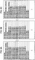
- Fig. 10 shows a state in which a defective block of a code area is substituted with a substitution area in the manner described above, the remaining substitution area becomes one block, a defect occurs in a block L (not shown) within the code area at that point in time, and the substitution area is used up. That is, the areas up to the substitution area 1 adjacent to the interference area 2 have been "used". Furthermore, as shown in block 11 of Fig. 10 , there is a case in which a block within the substitution area becomes defective. In this case, this defective block is stored in the information 155 on defective blocks ( Fig. 7 ) within the area for management and managed so that this block will not be used.
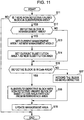
- Fig. 11 is a flowchart showing a schematic process of a defective block substitution process performed after a defective block is found. Defective blocks that occur late can be detected in steps S23 and S24 of Fig. 12 (to be described later) and in step S18 of Fig. 11 .
- Fig. 11 at first, it is checked whether or not an unused non-defective block exists in the substitution area (S11). If it does not exist, this processing is completed. At this time, some message, such as an error message, may be displayed on a display section.
- the process proceeds to step S15. If it is a block in the management area, the current interference area 1 is set as a new management area (S13), and the current substitution area 1 is set as a new interference area 2 (S14).
- step S15 It is checked in step S15 whether or not the defective block is a block in a code area.
- the management information is updated by considering the block (block in the substitution area) as being defective (S17), and the process proceeds to step S18.
- the defective block is a block in the code area
- the defective block is substituted for with an unused non-defective block of the substitution area, which is farthest from the interference area (S16).
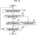
- Fig. 12 is a flowchart showing a process for updating a program within the NAND memory 15b on the basis of a file for updating.
- Fig. 13 shows the relationship between actual blocks corresponding to physical addresses of a NOR memory as a result of the substitution of a defective block and a code area corresponding to logical addresses.
- the correspondence between physical addresses and logical addresses of the NAND memory 15b based on the management information of the management area enables the continuity of the logical addresses to be ensured even when there is a defective block in the NAND memory of the program before updating. There is no need to shift the content of the block within the NAND memory 15b by using the file for updating, and the updating of the program becomes possible.
- Fig. 14 is a flowchart showing a process of reading the NAND memory 15b. At first, it is checked whether the block to be read has been substituted for on the basis of the management information (S31). If the block to be read has not been substituted for, the block to be read is read as it is (S32). If the block to be read has been substituted for, the substitution target block is read (S33). If there is another block to be read (S34), the process returns to step S31, and the above-described processing is repeated.
- the present invention has been described by using a portable phone terminal as an example. However, the present invention is not limited to a phone terminal.
- software difference updating has been described as a main application.
- the present invention is not limited to software difference updating, and can be generally applied to a case in which the content of some blocks of a NAND memory needs to be rewritten without exerting an influence on the other blocks.
- the present invention can be suitably applied to a NAND-type flash memory, but can also be applied to a NOR-type flash memory.
Landscapes
- Engineering & Computer Science (AREA)
- Theoretical Computer Science (AREA)
- General Engineering & Computer Science (AREA)
- Software Systems (AREA)
- General Physics & Mathematics (AREA)
- Physics & Mathematics (AREA)
- Computer Security & Cryptography (AREA)
- Computer Networks & Wireless Communication (AREA)
- Signal Processing (AREA)
- Techniques For Improving Reliability Of Storages (AREA)
- Memory System (AREA)
- For Increasing The Reliability Of Semiconductor Memories (AREA)
- Read Only Memory (AREA)
Applications Claiming Priority (1)
| Application Number | Priority Date | Filing Date | Title |
|---|---|---|---|
| JP2006212751A JP5019567B2 (ja) | 2006-08-04 | 2006-08-04 | メモリ管理方法および携帯端末装置 |
Publications (3)
| Publication Number | Publication Date |
|---|---|
| EP1909175A2 EP1909175A2 (en) | 2008-04-09 |
| EP1909175A3 EP1909175A3 (en) | 2009-05-27 |
| EP1909175B1 true EP1909175B1 (en) | 2018-08-22 |
Family
ID=38819896
Family Applications (1)
| Application Number | Title | Priority Date | Filing Date |
|---|---|---|---|
| EP07252969.6A Ceased EP1909175B1 (en) | 2006-08-04 | 2007-07-27 | Memory management method and portable terminal device |
Country Status (6)
| Country | Link |
|---|---|
| US (1) | US7797573B2 (ko) |
| EP (1) | EP1909175B1 (ko) |
| JP (1) | JP5019567B2 (ko) |
| KR (1) | KR20080012778A (ko) |
| CN (1) | CN100541450C (ko) |
| TW (1) | TW200828017A (ko) |
Families Citing this family (10)
| Publication number | Priority date | Publication date | Assignee | Title |
|---|---|---|---|---|
| US8446787B2 (en) * | 2008-11-20 | 2013-05-21 | Micron Technology, Inc. | Replacing defective memory blocks in response to external addresses |
| JP5521437B2 (ja) * | 2009-01-29 | 2014-06-11 | 日本電気株式会社 | 携帯端末装置、ソフトウェア更新方法及びプログラム |
| US8706954B2 (en) | 2010-09-07 | 2014-04-22 | Sony Corporation | Memory management apparatus and memory management method |
| CN108549609B (zh) * | 2011-09-30 | 2022-06-21 | 英特尔公司 | 作为传统大容量存储设备的替代的非易失性随机存取存储器(nvram) |
| US20150230080A1 (en) * | 2014-02-11 | 2015-08-13 | Pantech Co., Ltd. | Media scanning method and media scanning terminal |
| WO2015146788A1 (ja) * | 2014-03-28 | 2015-10-01 | 京セラドキュメントソリューションズ株式会社 | 電子機器 |
| US9760303B2 (en) * | 2015-09-29 | 2017-09-12 | Sandisk Technologies Llc | Partially-bad block operation in 3-D nonvolatile memory |
| CN106339242A (zh) * | 2016-07-26 | 2017-01-18 | 深圳市英威腾交通技术有限公司 | 一种电力机车控制设备的软件更新方法和系统 |
| CN106951297B (zh) * | 2017-04-06 | 2020-07-28 | 惠州佰维存储科技有限公司 | 嵌入式多媒体卡的生产方法及其系统 |
| JP7074454B2 (ja) * | 2017-10-30 | 2022-05-24 | キオクシア株式会社 | 計算機システムおよび制御方法 |
Citations (1)
| Publication number | Priority date | Publication date | Assignee | Title |
|---|---|---|---|---|
| US20040057316A1 (en) * | 2002-09-25 | 2004-03-25 | Renesas Technology Corp. | Nonvolatile memory |
Family Cites Families (15)
| Publication number | Priority date | Publication date | Assignee | Title |
|---|---|---|---|---|
| US6135651A (en) * | 1997-05-29 | 2000-10-24 | Cirrus Logic, Inc. | Patching apparatus and method for upgrading modem software code |
| JP2001134496A (ja) * | 1999-11-04 | 2001-05-18 | Hitachi Ltd | 不揮発性半導体メモリを用いた記憶装置 |
| US6601167B1 (en) * | 2000-01-14 | 2003-07-29 | Advanced Micro Devices, Inc. | Computer system initialization with boot program stored in sequential access memory, controlled by a boot loader to control and execute the boot program |
| JP2001350673A (ja) * | 2000-06-05 | 2001-12-21 | Hitachi Ltd | フラッシュメモリアクセス制御方法 |
| US6684289B1 (en) * | 2000-11-22 | 2004-01-27 | Sandisk Corporation | Techniques for operating non-volatile memory systems with data sectors having different sizes than the sizes of the pages and/or blocks of the memory |
| US7328007B2 (en) * | 2001-07-26 | 2008-02-05 | Kyocera Wireless Corp. | System and method for organizing wireless communication device system software |
| US6879530B2 (en) * | 2002-07-18 | 2005-04-12 | Micron Technology, Inc. | Apparatus for dynamically repairing a semiconductor memory |
| US7210010B2 (en) * | 2002-09-30 | 2007-04-24 | Insignia Solutions Plc | Efficient system and method for updating a memory device |
| GB2403303B (en) | 2003-06-23 | 2005-08-17 | Matsushita Electric Ind Co Ltd | Embedded device with software registry |
| JP4357305B2 (ja) * | 2004-01-09 | 2009-11-04 | 株式会社バッファロー | 外部記憶装置 |
| US7336536B2 (en) * | 2004-06-25 | 2008-02-26 | Micron Technology, Inc. | Handling defective memory blocks of NAND memory devices |
| US7212440B2 (en) * | 2004-12-30 | 2007-05-01 | Sandisk Corporation | On-chip data grouping and alignment |
| US20060184719A1 (en) * | 2005-02-16 | 2006-08-17 | Sinclair Alan W | Direct data file storage implementation techniques in flash memories |
| US20060282610A1 (en) * | 2005-06-08 | 2006-12-14 | M-Systems Flash Disk Pioneers Ltd. | Flash memory with programmable endurance |
| US7508708B2 (en) * | 2006-03-30 | 2009-03-24 | Micron Technology, Inc. | NAND string with a redundant memory cell |
-
2006
- 2006-08-04 JP JP2006212751A patent/JP5019567B2/ja active Active
-
2007
- 2007-07-26 TW TW096127329A patent/TW200828017A/zh unknown
- 2007-07-27 EP EP07252969.6A patent/EP1909175B1/en not_active Ceased
- 2007-07-31 US US11/882,175 patent/US7797573B2/en active Active
- 2007-08-02 KR KR1020070077679A patent/KR20080012778A/ko not_active Application Discontinuation
- 2007-08-06 CN CNB2007101438009A patent/CN100541450C/zh active Active
Patent Citations (1)
| Publication number | Priority date | Publication date | Assignee | Title |
|---|---|---|---|---|
| US20040057316A1 (en) * | 2002-09-25 | 2004-03-25 | Renesas Technology Corp. | Nonvolatile memory |
Also Published As
| Publication number | Publication date |
|---|---|
| US20080034252A1 (en) | 2008-02-07 |
| JP5019567B2 (ja) | 2012-09-05 |
| EP1909175A3 (en) | 2009-05-27 |
| JP2008040701A (ja) | 2008-02-21 |
| KR20080012778A (ko) | 2008-02-12 |
| CN101118518A (zh) | 2008-02-06 |
| EP1909175A2 (en) | 2008-04-09 |
| TW200828017A (en) | 2008-07-01 |
| CN100541450C (zh) | 2009-09-16 |
| US7797573B2 (en) | 2010-09-14 |
Similar Documents
| Publication | Publication Date | Title |
|---|---|---|
| EP1909175B1 (en) | Memory management method and portable terminal device | |
| CN100487672C (zh) | 用于分割一逻辑块的方法及设备 | |
| US8954649B2 (en) | Garbage collection in storage devices based on flash memories | |
| JP3892851B2 (ja) | メモリカード及び半導体装置 | |
| JP3708047B2 (ja) | フラッシュメモリの管理方法 | |
| US7174440B2 (en) | Method and apparatus for performing block caching in a non-volatile memory system | |
| US20080098195A1 (en) | Memory system including flash memory and mapping table management method | |
| US20080282024A1 (en) | Management of erase operations in storage devices based on flash memories | |
| US20060069849A1 (en) | Methods and apparatus to update information in a memory | |
| EP1895418A1 (en) | Nonvolatile memory device, method of writing data, and method of reading out data | |
| US20070214309A1 (en) | Nonvolatile storage device and data writing method thereof | |
| US8775758B2 (en) | Memory device and method for performing a write-abort-safe firmware update | |
| JP2013137771A (ja) | データ利用についてのマウント時間の調停 | |
| JP2004258946A (ja) | メモリカード | |
| JP5329689B2 (ja) | メモリコントローラ、不揮発性記憶装置 | |
| CN112596668A (zh) | 一种存储器的坏块处理方法及系统 | |
| JP2000222292A (ja) | フラッシュメモリを利用したデータ管理方法 | |
| US7234036B1 (en) | Method and apparatus for resolving physical blocks associated with a common logical block | |
| KR100825802B1 (ko) | 기입 데이터의 논리적 페이지보다 이전 논리적 페이지들을가지는 데이터들을 데이터 블록으로부터 복사하는 불휘발성메모리 장치의 데이터 기입 방법 | |
| JP2009134672A (ja) | メモリ管理方法および携帯端末装置 | |
| US8209475B2 (en) | Write timeout control methods for flash memory and memory devices using the same | |
| JP2009009390A (ja) | メモリ管理方法および携帯端末装置 | |
| JP2007066326A (ja) | 記憶装置、データ処理装置並びにデータ処理方法 | |
| CN116560700B (zh) | 芯片固件升级系统 | |
| KR100636522B1 (ko) | 백앤드칩이 장착된 이동통신 단말기로의 파일 다운로드 방법 |
Legal Events
| Date | Code | Title | Description |
|---|---|---|---|
| PUAI | Public reference made under article 153(3) epc to a published international application that has entered the european phase |
Free format text: ORIGINAL CODE: 0009012 |
|
| AK | Designated contracting states |
Kind code of ref document: A2 Designated state(s): AT BE BG CH CY CZ DE DK EE ES FI FR GB GR HU IE IS IT LI LT LU LV MC MT NL PL PT RO SE SI SK TR |
|
| AX | Request for extension of the european patent |
Extension state: AL BA HR MK RS |
|
| PUAL | Search report despatched |
Free format text: ORIGINAL CODE: 0009013 |
|
| AK | Designated contracting states |
Kind code of ref document: A3 Designated state(s): AT BE BG CH CY CZ DE DK EE ES FI FR GB GR HU IE IS IT LI LT LU LV MC MT NL PL PT RO SE SI SK TR |
|
| AX | Request for extension of the european patent |
Extension state: AL BA HR MK RS |
|
| 17P | Request for examination filed |
Effective date: 20090528 |
|
| 17Q | First examination report despatched |
Effective date: 20090713 |
|
| AKX | Designation fees paid |
Designated state(s): DE FR GB |
|
| RAP1 | Party data changed (applicant data changed or rights of an application transferred) |
Owner name: SONY MOBILE COMMUNICATIONS JAPAN, INC. |
|
| RAP1 | Party data changed (applicant data changed or rights of an application transferred) |
Owner name: SONY MOBILE COMMUNICATIONS, INC. |
|
| RAP1 | Party data changed (applicant data changed or rights of an application transferred) |
Owner name: SNAPTRACK, INC. |
|
| GRAP | Despatch of communication of intention to grant a patent |
Free format text: ORIGINAL CODE: EPIDOSNIGR1 |
|
| INTG | Intention to grant announced |
Effective date: 20180301 |
|
| GRAS | Grant fee paid |
Free format text: ORIGINAL CODE: EPIDOSNIGR3 |
|
| GRAA | (expected) grant |
Free format text: ORIGINAL CODE: 0009210 |
|
| AK | Designated contracting states |
Kind code of ref document: B1 Designated state(s): DE FR GB |
|
| REG | Reference to a national code |
Ref country code: GB Ref legal event code: FG4D |
|
| REG | Reference to a national code |
Ref country code: DE Ref legal event code: R096 Ref document number: 602007055825 Country of ref document: DE |
|
| REG | Reference to a national code |
Ref country code: DE Ref legal event code: R097 Ref document number: 602007055825 Country of ref document: DE |
|
| PLBE | No opposition filed within time limit |
Free format text: ORIGINAL CODE: 0009261 |
|
| STAA | Information on the status of an ep patent application or granted ep patent |
Free format text: STATUS: NO OPPOSITION FILED WITHIN TIME LIMIT |
|
| 26N | No opposition filed |
Effective date: 20190523 |
|
| PGFP | Annual fee paid to national office [announced via postgrant information from national office to epo] |
Ref country code: DE Payment date: 20190617 Year of fee payment: 13 |
|
| GBPC | Gb: european patent ceased through non-payment of renewal fee |
Effective date: 20190727 |
|
| PG25 | Lapsed in a contracting state [announced via postgrant information from national office to epo] |
Ref country code: GB Free format text: LAPSE BECAUSE OF NON-PAYMENT OF DUE FEES Effective date: 20190727 |
|
| PG25 | Lapsed in a contracting state [announced via postgrant information from national office to epo] |
Ref country code: FR Free format text: LAPSE BECAUSE OF NON-PAYMENT OF DUE FEES Effective date: 20190731 |
|
| REG | Reference to a national code |
Ref country code: DE Ref legal event code: R119 Ref document number: 602007055825 Country of ref document: DE |
|
| PG25 | Lapsed in a contracting state [announced via postgrant information from national office to epo] |
Ref country code: DE Free format text: LAPSE BECAUSE OF NON-PAYMENT OF DUE FEES Effective date: 20210202 |