EP1908147B1 - Antennenanordnung mit verschachtelten antennenelementen - Google Patents
Antennenanordnung mit verschachtelten antennenelementen Download PDFInfo
- Publication number
- EP1908147B1 EP1908147B1 EP06758086.0A EP06758086A EP1908147B1 EP 1908147 B1 EP1908147 B1 EP 1908147B1 EP 06758086 A EP06758086 A EP 06758086A EP 1908147 B1 EP1908147 B1 EP 1908147B1
- Authority
- EP
- European Patent Office
- Prior art keywords
- antenna
- mhz
- antenna elements
- frequency
- arrangement according
- Prior art date
- Legal status (The legal status is an assumption and is not a legal conclusion. Google has not performed a legal analysis and makes no representation as to the accuracy of the status listed.)
- Not-in-force
Links
Images


Classifications
-
- H—ELECTRICITY
- H01—ELECTRIC ELEMENTS
- H01Q—ANTENNAS, i.e. RADIO AERIALS
- H01Q21/00—Antenna arrays or systems
- H01Q21/06—Arrays of individually energised antenna units similarly polarised and spaced apart
- H01Q21/08—Arrays of individually energised antenna units similarly polarised and spaced apart the units being spaced along or adjacent to a rectilinear path
- H01Q21/10—Collinear arrangements of substantially straight elongated conductive units
-
- H—ELECTRICITY
- H01—ELECTRIC ELEMENTS
- H01Q—ANTENNAS, i.e. RADIO AERIALS
- H01Q1/00—Details of, or arrangements associated with, antennas
- H01Q1/52—Means for reducing coupling between antennas; Means for reducing coupling between an antenna and another structure
- H01Q1/521—Means for reducing coupling between antennas; Means for reducing coupling between an antenna and another structure reducing the coupling between adjacent antennas
- H01Q1/523—Means for reducing coupling between antennas; Means for reducing coupling between an antenna and another structure reducing the coupling between adjacent antennas between antennas of an array
-
- H—ELECTRICITY
- H01—ELECTRIC ELEMENTS
- H01Q—ANTENNAS, i.e. RADIO AERIALS
- H01Q1/00—Details of, or arrangements associated with, antennas
- H01Q1/12—Supports; Mounting means
- H01Q1/22—Supports; Mounting means by structural association with other equipment or articles
- H01Q1/2208—Supports; Mounting means by structural association with other equipment or articles associated with components used in interrogation type services, i.e. in systems for information exchange between an interrogator/reader and a tag/transponder, e.g. in Radio Frequency Identification [RFID] systems
- H01Q1/2216—Supports; Mounting means by structural association with other equipment or articles associated with components used in interrogation type services, i.e. in systems for information exchange between an interrogator/reader and a tag/transponder, e.g. in Radio Frequency Identification [RFID] systems used in interrogator/reader equipment
-
- H—ELECTRICITY
- H01—ELECTRIC ELEMENTS
- H01Q—ANTENNAS, i.e. RADIO AERIALS
- H01Q1/00—Details of, or arrangements associated with, antennas
- H01Q1/12—Supports; Mounting means
- H01Q1/22—Supports; Mounting means by structural association with other equipment or articles
- H01Q1/24—Supports; Mounting means by structural association with other equipment or articles with receiving set
- H01Q1/241—Supports; Mounting means by structural association with other equipment or articles with receiving set used in mobile communications, e.g. GSM
- H01Q1/246—Supports; Mounting means by structural association with other equipment or articles with receiving set used in mobile communications, e.g. GSM specially adapted for base stations
-
- H—ELECTRICITY
- H01—ELECTRIC ELEMENTS
- H01Q—ANTENNAS, i.e. RADIO AERIALS
- H01Q1/00—Details of, or arrangements associated with, antennas
- H01Q1/52—Means for reducing coupling between antennas; Means for reducing coupling between an antenna and another structure
- H01Q1/526—Electromagnetic shields
-
- H—ELECTRICITY
- H01—ELECTRIC ELEMENTS
- H01Q—ANTENNAS, i.e. RADIO AERIALS
- H01Q15/00—Devices for reflection, refraction, diffraction or polarisation of waves radiated from an antenna, e.g. quasi-optical devices
- H01Q15/14—Reflecting surfaces; Equivalent structures
- H01Q15/16—Reflecting surfaces; Equivalent structures curved in two dimensions [2D], e.g. paraboloidal
- H01Q15/165—Reflecting surfaces; Equivalent structures curved in two dimensions [2D], e.g. paraboloidal composed of a plurality of rigid panels
- H01Q15/166—Reflecting surfaces; Equivalent structures curved in two dimensions [2D], e.g. paraboloidal composed of a plurality of rigid panels sector shaped
-
- H—ELECTRICITY
- H01—ELECTRIC ELEMENTS
- H01Q—ANTENNAS, i.e. RADIO AERIALS
- H01Q19/00—Combinations of primary active antenna elements and units with secondary devices, e.g. with quasi-optical devices, for giving the antenna a desired directional characteristic
- H01Q19/10—Combinations of primary active antenna elements and units with secondary devices, e.g. with quasi-optical devices, for giving the antenna a desired directional characteristic using reflecting surfaces
- H01Q19/104—Combinations of primary active antenna elements and units with secondary devices, e.g. with quasi-optical devices, for giving the antenna a desired directional characteristic using reflecting surfaces using a substantially flat reflector for deflecting the radiated beam, e.g. periscopic antennas
-
- H—ELECTRICITY
- H01—ELECTRIC ELEMENTS
- H01Q—ANTENNAS, i.e. RADIO AERIALS
- H01Q21/00—Antenna arrays or systems
- H01Q21/06—Arrays of individually energised antenna units similarly polarised and spaced apart
- H01Q21/08—Arrays of individually energised antenna units similarly polarised and spaced apart the units being spaced along or adjacent to a rectilinear path
-
- H—ELECTRICITY
- H01—ELECTRIC ELEMENTS
- H01Q—ANTENNAS, i.e. RADIO AERIALS
- H01Q21/00—Antenna arrays or systems
- H01Q21/24—Combinations of antenna units polarised in different directions for transmitting or receiving circularly and elliptically polarised waves or waves linearly polarised in any direction
- H01Q21/26—Turnstile or like antennas comprising arrangements of three or more elongated elements disposed radially and symmetrically in a horizontal plane about a common centre
-
- H—ELECTRICITY
- H01—ELECTRIC ELEMENTS
- H01Q—ANTENNAS, i.e. RADIO AERIALS
- H01Q21/00—Antenna arrays or systems
- H01Q21/28—Combinations of substantially independent non-interacting antenna units or systems
-
- H—ELECTRICITY
- H01—ELECTRIC ELEMENTS
- H01Q—ANTENNAS, i.e. RADIO AERIALS
- H01Q21/00—Antenna arrays or systems
- H01Q21/30—Combinations of separate antenna units operating in different wavebands and connected to a common feeder system
-
- H—ELECTRICITY
- H01—ELECTRIC ELEMENTS
- H01Q—ANTENNAS, i.e. RADIO AERIALS
- H01Q5/00—Arrangements for simultaneous operation of antennas on two or more different wavebands, e.g. dual-band or multi-band arrangements
- H01Q5/40—Imbricated or interleaved structures; Combined or electromagnetically coupled arrangements, e.g. comprising two or more non-connected fed radiating elements
- H01Q5/42—Imbricated or interleaved structures; Combined or electromagnetically coupled arrangements, e.g. comprising two or more non-connected fed radiating elements using two or more imbricated arrays
-
- H—ELECTRICITY
- H01—ELECTRIC ELEMENTS
- H01Q—ANTENNAS, i.e. RADIO AERIALS
- H01Q9/00—Electrically-short antennas having dimensions not more than twice the operating wavelength and consisting of conductive active radiating elements
- H01Q9/04—Resonant antennas
Definitions
- the present invention relates to an antenna arrangement with interleaved antenna elements for multiple frequency band operation, especially for mobile communication systems, as defined in the preamble of claim 1.
- the invention also relates to an antenna system being adapted to communicate through a communication link with a base station.
- Present antenna arrays used for transmitting and receiving RF (Radio Frequency) signals in mobile communication systems are normally dedicated to a single frequency band or sometimes two or more frequency bands.
- Single frequency band antennas have been used for a long time and normally include a number of antenna elements arranged in a vertical row. A second row of antenna elements needs to be added beside the first row if the operator in a network wants to add another frequency band using single frequency band antennas.
- this requires enough space to implement and the arrangement may also be sensitive to interference between the RF signals in the different frequency bands.
- a first antenna element 11 is a dual band antenna element which operates in two different frequency bands FB 1 and FB 2
- a second antenna element 12 is an antenna element which operates in only one frequency band FB 1 .
- a drawback with this prior art embodiment is that the frequency bands FB 1 and FB 2 will couple to each other due to the closeness of the parts making up the antenna element 11.
- this kind of configuration is only suitable when the frequency bands have a big separation, for example if FB2 is approximately twice the frequency as FB 1 . If the frequency bands are too close, filters with high Q values, for example cavity filters which consume space and are relatively expensive and heavy, must be used very close to the antenna elements.
- the prior art arrangement shown in figure IB is formed by an array including first antenna elements, 11a, which are positioned in two parallel columns 13a, 14a and operate in a first, lower frequency band, and second antenna elements 12a, which are alternately located in two adjacent columns 13a, 15a and operate in a second, higher frequency band.
- first antenna elements, 11a which are positioned in two parallel columns 13a, 14a and operate in a first, lower frequency band
- second antenna elements 12a which are alternately located in two adjacent columns 13a, 15a and operate in a second, higher frequency band.
- One of these adjacent columns (13a) is the same as one of the columns accommodating the first antenna elements 11a, whereas the other column 15a is located between the columns 13a, 14a.
- EP 1 227 545 A1 relates to antenna arrays which can work simultaneously in various frequency bands thanks to the physical disposition of the elements which constitute them, and also the multiband behaviour of some elements situated strategically in the array.
- the configuration of the array is described based on the juxtaposition or interleaving of various conventional mono-band arrays working in the different bands of interest. In those positions in which elements of different multiband arrays come together, a multiband antenna is employed which covers the different working frequency bands.
- US 2003/0137456 A1 relates to a dual band coplanar microstrip interlaced array antenna.
- the antenna may be confined to a relatively small area, while providing dual band operation with no or minimal grating lobes and losses.
- First and second arrays are interlaced with one another to minimize the surface area of the antenna.
- a maximum spacing between array elements is selected based on the operating wavelengths and scan range for each of the arrays.
- a first dielectric constant of a material underlying elements of the first array is calculated from the selected element spacing and the operating wavelength of the first array.
- a second dielectric constant of a material underlying elements of the second array is calculated from the first dielectric constant and the operating frequencies of the first and second arrays.
- An object with the present invention is to provide a multiple frequency band antenna arrangement, and an antenna system, that will reduce the coupling between different frequency bands while at the same time minimizing the space needed compared to prior art antennas.
- the object is achieved for a multiple frequency band antenna arrangement according to independent claim 1.
- the antenna arrangement is connectable to a transceiver for transmitting and receiving RF signals in at least two separate frequency regions.
- the antenna arrangement has at least two sets of antenna elements arranged on a reflector. A first set of antenna elements is arranged in a column and operates in a first frequency region, whereas a second set of antenna elements is likewise arranged in a column and operates in a second frequency region.
- the first and second sets of antenna elements are interleaved along and positioned on a straight line so as to form a single column, said first and second frequency regions including first and second frequency bands, respectively, which are separate and substantially non-overlapping but relatively close to each other, and wherein each of the antenna elements operates in only one frequency band, and the distance between adjacent antenna elements in said column, operating in different frequency bands, are substantially the same along said column and is smaller than the wavelength ⁇ of the centre frequency of the highest one of said first and second frequency bands. All antenna elements of the antenna arrangement are arranged in the above mentioned single column.
- an antenna system being adapted to communicate through a communication link with a base station, wherein the antenna system comprises an antenna arrangement, and means for controlling the phase and amplitude of transmitting signals and receiving signals to/from antenna elements in said antenna arrangement.
- An advantage with the present invention is that an isolation of more than 30 dB between the frequency bands can be obtained, without the use of cavity filters even if the frequency bands are close to each other.
- Another advantage with the present invention is that it is easy to configure an antenna having a desired selection of frequency bands.
- Still another advantage with the present invention is that the size of the antenna arrangement is maintained small compared to prior art arrangements.
- FIG. 2A shows a schematic representation of a dual band antenna arrangement 20, according to the present invention, operating in two frequency regions including first and second frequency bands FB 1 and FB 2 which are separate and substantially non-overlapping but relatively close to each other.
- the antenna elements 21 (marked with continuous lines) operating in the lower frequency band FB 1 is of a first type and the antenna elements 22 (marked with dashed lines) operating in the higher frequency band FB 2 is of a second type.
- the modified version of the dual band antenna arrangement 25, shown in figure 2B is basically the same as the one shown in figure 2A , the only difference being that cross polarised antenna elements 26 are interleaved with linear y polarised antenna elements 27.
- FIG 2C there is illustrated how the two frequency bands are "substantially non-overlapping".
- the input reflection coefficient for the antenna elements 21 ( figure 2A ) in the lower frequency range is represented by the S-parameter S 11
- the input reflection coefficient for the antenna elements 22 in the higher frequency range is represented by the C-parameter S 22 .
- the reflection coefficient should be less than -15 dB (R max ).
- the cross-coupling coefficient between the two frequency ranges should also be low, say less than -20 dB (C max ).
- each antenna element could be patches, dipoles, cross polarized antenna elements, dielectric resonator antennas (DRA) or any other type of antenna elements available to the skilled person.
- the essential feature of the invention is that each antenna element operates in only one frequency band and that they are arranged on a reflector in an interleaved configuration along a straight line, in a single column, as illustrated in figure 2 .
- Figures 3 , 4 and 5 show different embodiments of the schematic representation in figure 2 .
- Figure 3 shows a dual band antenna arrangement 30 having a first type of antenna elements 31 implemented as a double patch antenna element transmitting and receiving within a lower frequency band FB 1 .
- a second type of antenna element 32 is implemented as a patch antenna element transmitting and receiving within a higher frequency band FB 2 .
- An example of a lower frequency band could be 1710-2170 MHz and an example of a higher frequency band could be 2.5-2.7 GHz. Both types of antenna elements are known to those skilled in the art.
- a first distance "y”, between antenna elements 31 that operate within the same frequency band, namely the lower frequency band, is in the range of a distance that corresponds to 0.5-0.9 lambda ( ⁇ ) of the centre frequency of that (lower) frequency band.
- a second distance "z”, between antenna elements 32 that operate within the higher frequency band is in the range of a distance that corresponds to 0.5-0.9 lambda ( ⁇ ) of the centre frequency of that (higher) frequency band.
- the distance y may be different from the distance z, but since this will give rise to undesired effects, it is preferred that the distance y is equal to z. As an example y and z are selected to be approx. 100 mm each.
- the embodiment described in connection with figure 3 contains types of antenna elements that are rather large and there may be a problem concerning the appearance of grating lobes that will occur when two antenna elements are placed too far from each other.
- FIG 4 a perspective view of a second embodiment of a dual band antenna array 40 is shown.
- the dual band antenna array 40 contains two types of antenna elements, a first type 41 for the lower frequency band and a second type 42 for the higher frequency band.
- the first type of antenna elements 41 only receives RF signals within a range of 1920-1980 MHz and the second type of antenna elements 42 only transmits RF signals within a range of 2110-2170 MHz, which leaves a suppressed frequency band of 130 MHz therebetween.
- a traditional antenna for the UMTS band is replaced by a dual band antenna with separate antenna elements for the R x band and T x band, respectively, so that simplified T x and R x radio chains can be realized.
- Both types 41 and 42 of antenna elements are made of a DRA (Dielectric Resonator Antenna) which are considerable smaller than conventional patch antennas.
- DRA Dielectric Resonator Antenna
- the drawback with the DRA is that they might have a narrow bandwidth compared to other types of antenna elements, but if used only for reception or transmission they will operate in a desired way.
- the size of the DRA compared to patches, as described in connection with figure 3 will minimize the appearance of grating lobes since the antenna elements can be placed closer together compared to the antenna elements described in connection with figure 2 .
- FIG 5 a perspective view of a third embodiment of a dual band antenna array 50 is shown.
- the dual band antenna array 50 contains two types of antenna elements, a first type 51 for the lower frequency band and a second type 52 for the higher frequency band.
- the first type of antenna elements 51 transmits and receives RF signals within a range of 1710-2170 MHz, which is similar to the antenna element 31 described in connection with figure 3 .
- the second type of antenna elements 52 transmits and receives RF signals within a range of 2.5-2.7 GHz, which is the same frequency band as antenna element 32 ( fig. 3 ) operated within.
- a difference between the previously described antenna element 32 and the antenna element 52 is the type of antenna element being used.
- a DRA is used as the second type of antenna element.
- the DRA might have a narrow bandwidth, the second antenna element will be sufficient to ensure proper operation.
- a shielding wall 53 is provided between each antenna element 51, 52, with the distances (x, y and z) maintained as described in connection with figure 3 .
- DAA Dielectric Resonator Antennas
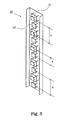
- Figures 6 and 7 show an embodiment of a multi band antenna array 60 of the present invention including three different frequency bands.
- This embodiment includes three types of antenna elements, a first type 61 for a lower frequency band FB 1 a second type 62 for a middle frequency band FB 2 and a third type 63 for a higher (or even lower) frequency band FB 3 .
- the following combinations of centre frequencies f1, f2, f3 are possible:
- a first distance "y”, between two antenna elements 61 that operate within the lower frequency band, is preferably a distance that corresponds to 0.5-0.9 lambda of the centre frequency of the lower frequency band, i.e. 1940 MHz in this example.
- a second distance "z”, between two antenna elements 62 that operate within the middle frequency band, is preferably a distance that corresponds to 0.5-0.9 lambda of the centre frequency, i.e. 2.35 GHz in this example, of the middle frequency band.
- a third distance "w”, between two antenna elements 63 that operate within the higher frequency band is preferably a distance that corresponds to 0.5-0.9 lambda of the centre frequency, i.e. 2.6 GHz in this example, of the higher frequency band.
- the distances y, z and w may be differ somewhat from each other, but since this will give rise to undesired effects, it is preferred that the distances y, z and w are equal to each other.
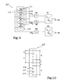
- FIG 8 shows a block diagram illustrating the signal path in an antenna system 80 according to the present invention.
- the signal path can be divided into a transmission path T x and a reception path R x that are connected to a separate antenna element 81 and 82 for each path as illustrated in the drawing or a common antenna element (not shown).
- the reception path R x comprises a band pass filter BP 1 to filter out the desired Radio frequency (RF) band connected in series with an optional low pass filter LP to remove spurious resonances before the filtered RF signal is fed into a Low Noise Amplifier LNA.
- the amplified RF signal is frequency shifted to an IF (Intermediate Frequency) signal using a Local Oscillator LO and a mixer 83.
- the IF signal is thereafter converted to a digital signal using an arrangement including an Analogue-to-Digital Converter (ADC).
- ADC Analogue-to-Digital Converter
- the first option includes a Wideband A/D Converter W/ADC that converts the complete RF band into a digital stream of 16 s/c (samples/chip).
- the second option includes several single carrier A/D Converter SC/ADC that together converts the complete RF band into a digital stream of 16 s/c.
- the 16 s/c digital signal in the first and second option is thereafter fed into a digital filter DF and a Digital Down Converter DDC.
- the DDC converts the 16 s/c signal to a 7 s/c signal which is fed to a digital phase shifter DPS which receives control signals, preferably in digital form.
- the control signals are received from a connected base station (not shown) through a communication line, such as a fibre 85.
- DPS controls the phase ⁇ and amplitude ⁇ of the digitized IF signal.
- the signal from the DPS is fed into a summation module 84 together with signals from other optional antenna elements.
- the third option for converting the IF signal to a digitized signal include an analogue phase shifter APS, to which control signals, preferably in analogue form, are fed that are received from a connected base station (not shown) through a communication line, such as a fibre 85.
- APS controls the phase ⁇ and amplitude ⁇ of the IF signal which is digitized using a following Analogue-to-Digital Converter ADC which converts the signal into a digital stream of 16 s/c.
- the 16 s/c digital signal in the third option is thereafter fed into a digital filter DF and a Digital Down Converter DDC.
- the DDC converts the 16 s/c signal to a 7 s/c signal and is fed into the summation module 84 together with signals from other optional antenna elements.
- Digital I and Q signals of 2 s/c are thereafter sent to the base station through the fibre 85.
- Communication through the fibre may use CPRI-standard communication protocols.
- the base station also supplies a digital I and Q signal of 1 s/c for transmission to a splitter 86.
- the signal can be controlled in a digital or an analogue way, both being described in connection with figure 8 .
- the signal from the splitter 86 is fed to a Digital Phase Shifter DPS, which is supplied with digital control signals for controlling the phase ⁇ and amplitude ⁇ of the transmission signal from the base station through the fibre 85.
- the signal is then fed to a device 87 for Digital Up Conversion DUC, a Digital Predistortion PDP and Crest Factor Reduction CFR is thereafter connected to the digital transmission signal.
- the DUC converts the signal to 16 s/c from 7 s/c.
- the DPD is used to obtain a linear signal after the signal is amplified and CFR is used to limit the peak in the signal to optimize the performance of the amplifier AMP.
- the digital signal is thereafter processed in a Digital/Analogue Converter DAC to an IF transmission signal.
- the signal is fed to a device 87 for Digital Up Convertion DUC, a Digital Predistortion PDP and Crest Factor Reduction CFR is thereafter connected to the digital transmission signal.
- the digital signal is thereafter processed in a Digital/Analogue Converter DAC to an IF transmission signal, and is thereafter fed to an Analogue Phase Shifter APS, which is supplied with analogue control signals for controlling the phase ⁇ and amplitude ⁇ of the transmission signal from the base station through the fibre 85.
- the signal is then frequency shifted to a RF transmission signal using a local oscillator LO and a mixer 88.
- the RF transmission signal is amplified in an amplifier AMP with a following optional filter F.
- a band pass filter BF 2 completes the transmission path, where the desired radio frequency band is selected before transmission via the antenna element 82.
- the RF signal is sensed before the band pass filter BF 2 and frequency shifted to an IF feedback signal using a local oscillator LO and a mixer 89.
- the IF feedback signal is converted to a digital signal, using a Digital-to-Analogue Converter DAC, and fed into the DPD in the device 87.
- the same local oscillator LO is used for the transmission path.
- different antenna elements 81, 82 are used for transmission and reception of the signals, but naturally a common antenna element may be used for both transmission and reception.
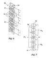
- Figure 9 shows a schematic representation of a second embodiment of a multi band antenna array 110 including additional filters LP, BP, and HP to provide a better isolation between the operating frequency bands FB 1 , FB 2 , and FB 3 for the antenna arrangement.
- the antenna arrangement 110 comprises two types of antenna elements, where a first antenna element 111 is a dual band antenna element receiving RF signals in a first frequency band FB 1 , and transmitting RF signals in a second frequency band FB 2 .
- the RF signals received in the first frequency band FB 1 is fed to a low pass filter LP, or a band pass filter for low frequencies, and thereafter to a first transceiver circuit T1.
- Transmitting RF signals from the first transceiver circuit T1 are fed to a band pass filter BP and thereafter to the dual band antenna element 111.
- the second type of antenna element 112 is operating within a third, higher frequency band FB 3 , i.e. both receiving and transmitting RF signals within FB 3 .
- RF signals to/from the antenna element 112 is fed through a high pass filter HP, or a band pass filter for high frequencies, to/from a second transceiver circuit T2.
- Transceiver circuits T1 and T2 are connected to a base station BS (not shown).
- Suppression means in the form of metallic strips 113 are arranged between each antenna element 111, 112, to shield the antenna elements from each other.
- Each metallic strip is fastened to the reflector 114 in an isolating way, e.g. using a dielectric material disposed therebetween.
- the filters will provide an increased isolation of more than 30 dB, whereas the construction in itself may only give an isolation of 15-20 dB.
- Figure 10 shows a schematic representation of a third embodiment of a multi band antenna arrangement 115, comprising three types of DRA antenna elements 116, 117, and 118. These elements are interleaved in such a way that two antenna elements of different type are arranged between two antenna elements of the same type.
- the distances y, z, and w are preferably the same as described in connection with figure 6 and the distances x between adjacent antenna element 116, 117 and 118 is preferably equal to each other.
- FIG 11 A suitable means to further increase the isolation between the frequency bands in a multi-band antenna is illustrated in figure 11 .
- the figure shows a communication system 100 having a dual band antenna arrangement 101, such as any of those illustrated in connection with figures 2A, 2B , 3 , 4, and 5 , with a low pass filter, (or band pass filter), LP between each antenna element 102 operating in the low frequency band and the transceiver circuitry T1 for the low frequency band, and a high pass filter, (or band pass filter), HP between each antenna element 103 operating in the high frequency band and the transceiver circuitry T2 for the high frequency band.
- Each transceiver circuitry T1, T2 is illustrated in connection with figure 8 and is connected to a base station BS, which is connected to the PSTN as is well-known to a person skilled in the art.
- the antenna system 100 also includes a device for Remote Electrical Tilt RET, which is controlled by the base station BS. RET controls an actuator 104 that will change the electrical tilt of the lobes from the antenna 101, as is well-known to those skilled in the art.
- RET Remote Electrical Tilt RET
- each antenna element operating at an intermediate frequency band is provided with a band pass filter to increase the isolation to the lower and higher frequency bands.
- the filters will provide an increased isolation of more than 30 dB, whereas the construction in it self may only give an isolation of 15-20 dB.
- the feeding of the antenna elements may include probe feeding, aperture feeding for all types of contemplated antenna elements, such as Patch antennas, DRA, Dipole antennas, cross polarized antennas.
Landscapes
- Physics & Mathematics (AREA)
- Electromagnetism (AREA)
- Engineering & Computer Science (AREA)
- Computer Networks & Wireless Communication (AREA)
- Variable-Direction Aerials And Aerial Arrays (AREA)
Claims (19)
- Antennenanordnung (20, 30, 40, 50, 60), welche an einen Sendeempfänger zum Senden und Empfangen von HF-Signalen in mindestens zwei getrennten Frequenzbändern anschließbar ist, wobei die Antennenanordnung Folgendes umfasst:einen ersten Satz Antennenelemente (21, 31, 41, 51) und einen zweiten Satz Antennenelemente (22, 32, 42, 52) in einer verschachtelten Anordnung auf einem Reflektor, wobei der erste und der zweite Satz Antennenelemente entlang einer geraden Linie verschachtelt und auf dieser angeordnet sind, um so eine einzelne Säule auszubilden;wobei der erste Satz Antennenelemente (21, 31, 41, 51) in einem ersten Frequenzbereich arbeitet, wohingegen der zweite Satz Antennenelemente (22, 42) in einem zweiten Frequenzbereich arbeitet,wobei der erste und der zweite Frequenzbereich ein erstes bzw. ein zweites Frequenzband (FB1, FB2) aufweisen, welche getrennt und im Wesentlichen nicht überlappend jedoch relativ nahe beieinander sind, und wobei jedes der Antennenelemente in nur einem Frequenzband arbeitet;die Entfernung (x) zwischen benachbarten Antennenelementen in der Säule, welche in verschiedenen Frequenzbändern arbeiten, entlang der Säule im Wesentlichen gleich ist und kleiner ist als die Wellenlänge λ der Mittenfrequenz des höchsten von dem ersten und dem zweiten Frequenzband,dadurch gekennzeichnet, dassalle Antennenelemente der Antennenanordnung (20, 30, 40, 50, 60) in der einzelnen Säule angeordnet sind.
- Antennenanordnung nach Anspruch 1, wobei die Mittenfrequenzen f1 und f2 des ersten und des zweiten Frequenzbandes in folgender Beziehung stehen:2/3 < f1 / f2 < 3/2, undf1 ist verschieden von f2.
- Antennenanordnung nach Anspruch 1, wobei die Entfernung (x) zwischen benachbarten Antennenelementen in der einzelnen Säule im Bereich von 0,3 bis 0,7 λ liegt.
- Antennenanordnung nach Anspruch 3, wobei die Entfernung (x) zwischen benachbarten Antennenelementen in der einzelnen Säule im Bereich von 28 bis 54 mm liegt.
- Antennenanordnung nach Anspruch 1, wobei die erste und die zweite Mittenfrequenz ungefähre Werte in einer der folgenden Kombinationen aufweisen:f1 = 850 MHz, f2 = 900 MHzf1 = 1.800 MHz, f2 = 2.000 MHzf1 = 1.900 MHz, f2 = 2.100 MHzf1 = 2.000 MHz, f2 = 2.500 MHz.
- Antennenanordnung nach Anspruch 1, wobei die einzelne Säule aus Antennenelementen auch einen dritten Satz Antennenelemente (63) aufweist, welche in einem dritten Frequenzbereich arbeiten, welcher ein Frequenzband umfasst, welches in Bezug auf das erste und das zweite Frequenzband getrennt und nicht überlappend ist, wobei die Mittenfrequenz des dritten Frequenzbandes höher oder niedriger ist als die Mittenfrequenzen des ersten und des zweiten Frequenzbandes.
- Antennenanordnung nach Anspruch 6, wobei der erste, der zweite und der dritte Satz Antennenelemente (61, 62, 63) in getrennten Frequenzbändern arbeiten, wobei die Mittenfrequenzen f1, f2, f3 ungefähre Werte in einer der folgenden Kombinationen aufweisen:f1 = 850 MHz, f2 = 900 MHz, f3 = 1.800 MHzf1 = 850 MHz, f2 = 900 MHz, f3 = 1.900 MHzf1 = 850 MHz, f2 = 900 MHz, f3 = 2.000 MHzf1 = 1.800 MHz, f2 = 2.000 MHz, f3 = 2.500 MHzf1 = 2.000 MHz, f2 = 2.500 MHz, f3 = 900 MHz.
- Antennenanordnung nach Anspruch 6, wobei die Antennenelemente des dritten Satzes (63) an den gleichen Positionen angeordnet sind wie mindestens einige der Antennenelemente des ersten und des zweiten Satzes (61, 62).
- Antennenanordnung nach Anspruch 6, wobei die Antennenelemente des dritten Satzes (63) an Positionen angeordnet sind, welche verschieden von denjenigen der Antennenelemente des ersten und des zweiten Satzes (61, 62) sind, wobei der dritte Satz Antennenelemente auch zwischen Antennenelementen des ersten und des zweiten Satzes verschachtelt ist.
- Antennenanordnung nach Anspruch 1, wobei mindestens einige der Antennenelemente dual polarisiert sind mit sich gegenseitig kreuzenden Polarisierungen.
- Antennenanordnung nach Anspruch 1, wobei mindestens einige der Antennenelemente linear polarisiert sind.
- Antennenanordnung nach Anspruch 1, wobei der erste und der zweite Satz Antennenelemente zum Senden von HF-Signalen (Tx) bzw. zum Empfangen von HF-Signalen (Rx) verwendet werden.
- Antennenanordnung nach Anspruch 1, wobei eine Entfernung (y, z, w) zwischen zwei Antennenelementen, welche in der einzelnen Säule angeordnet sind und in dem gleichen Frequenzband arbeiten, im Bereich einer Entfernung liegt, welche 0,5 bis 0,9 λ der Mittenfrequenz des jeweiligen Bandes entspricht.
- Antennenanordnung nach Anspruch 1, wobei mindestens einer der mindestens zwei Sätze Antennenelemente eine der folgenden Arten von Antennenelementen ist:- ein dielektrisches Resonatorantennen-(DRA)-Element,- ein Dipolantennenelement, oder- ein Patch-Antennenelement.
- Antennenanordnung nach Anspruch 1, wobei eine Kopplung zwischen den getrennten Frequenzbändern (FB1, FB2, FB3) durch Bereitstellen eines Unterdrückungsmittels (53; 64; 93, 94; 113) zwischen benachbarten Antennenelementen unterdrückt wird.
- Antennenanordnung nach Anspruch 15, wobei das Unterdrückungsmittel ein parasitisches Element ist, wie beispielsweise ein metallischer Streifen (113).
- Antennenanordnung nach Anspruch 15, wobei das Unterdrückungsmittel eine Abschirmwand (53; 64; 93, 94) ist.
- Antennenanordnung nach Anspruch 1, wobei ein Filter (LP, BP, HP) mit einem niedrigen Q-Wert zwischen jedem Antennenelement (102, 103; 111, 112) und einer Sendeempfängerschaltung (T1, T2) angeschlossen ist, wobei der Filter eingerichtet ist, um jedes Frequenzband (FB1, FB2, FB3) weiter voneinander zu isolieren.
- Antennensystem (80), welches eingerichtet ist, um durch eine Kommunikationsverbindung (85) mit einer Basisstation (BS) zu kommunizieren, umfassend eine Antennenanordnung nach einem der Ansprüche 1 bis 8 und Mittel zum Steuern der Phase und der Amplitude (APS; DPS) der Sendesignale und der Empfangssignale zu/von Antennenelementen (81, 82) in der Antennenanordnung.
Applications Claiming Priority (2)
| Application Number | Priority Date | Filing Date | Title |
|---|---|---|---|
| SE0501723 | 2005-07-22 | ||
| PCT/SE2006/000904 WO2007011295A1 (en) | 2005-07-22 | 2006-07-21 | Antenna arrangement with interleaved antenna elements |
Publications (3)
| Publication Number | Publication Date |
|---|---|
| EP1908147A1 EP1908147A1 (de) | 2008-04-09 |
| EP1908147A4 EP1908147A4 (de) | 2012-09-26 |
| EP1908147B1 true EP1908147B1 (de) | 2015-08-19 |
Family
ID=37669088
Family Applications (1)
| Application Number | Title | Priority Date | Filing Date |
|---|---|---|---|
| EP06758086.0A Not-in-force EP1908147B1 (de) | 2005-07-22 | 2006-07-21 | Antennenanordnung mit verschachtelten antennenelementen |
Country Status (4)
| Country | Link |
|---|---|
| US (1) | US7808443B2 (de) |
| EP (1) | EP1908147B1 (de) |
| CN (1) | CN107425296B (de) |
| WO (1) | WO2007011295A1 (de) |
Cited By (3)
| Publication number | Priority date | Publication date | Assignee | Title |
|---|---|---|---|---|
| WO2018149689A1 (de) | 2017-02-16 | 2018-08-23 | Kathrein Werke Kg | Antennenvorrichtung und antennenarray |
| US10680348B2 (en) | 2016-09-16 | 2020-06-09 | Taoglas Group Holdings Limited | Multi antenna for rail applications and methods |
| EP3534459B1 (de) * | 2018-03-02 | 2025-11-26 | PCTEL, Inc. | Systeme und verfahren zur reduzierung der signalstrahlung in einer unerwünschten richtung |
Families Citing this family (112)
| Publication number | Priority date | Publication date | Assignee | Title |
|---|---|---|---|---|
| EP1784894A1 (de) | 2004-08-31 | 2007-05-16 | Fractus, S.A. | Schlanke mehrbandantennengruppe für zellulare basisstationen |
| WO2007042938A2 (en) | 2005-10-14 | 2007-04-19 | Fractus, Sa | Slim triple band antenna array for cellular base stations |
| US7787823B2 (en) | 2006-09-15 | 2010-08-31 | Corning Cable Systems Llc | Radio-over-fiber (RoF) optical fiber cable system with transponder diversity and RoF wireless picocellular system using same |
| US7848654B2 (en) | 2006-09-28 | 2010-12-07 | Corning Cable Systems Llc | Radio-over-fiber (RoF) wireless picocellular system with combined picocells |
| US8873585B2 (en) | 2006-12-19 | 2014-10-28 | Corning Optical Communications Wireless Ltd | Distributed antenna system for MIMO technologies |
| US8111998B2 (en) | 2007-02-06 | 2012-02-07 | Corning Cable Systems Llc | Transponder systems and methods for radio-over-fiber (RoF) wireless picocellular systems |
| US20100054746A1 (en) | 2007-07-24 | 2010-03-04 | Eric Raymond Logan | Multi-port accumulator for radio-over-fiber (RoF) wireless picocellular systems |
| US8175459B2 (en) | 2007-10-12 | 2012-05-08 | Corning Cable Systems Llc | Hybrid wireless/wired RoF transponder and hybrid RoF communication system using same |
| WO2009081376A2 (en) | 2007-12-20 | 2009-07-02 | Mobileaccess Networks Ltd. | Extending outdoor location based services and applications into enclosed areas |
| EP2394379B1 (de) | 2009-02-03 | 2016-12-28 | Corning Optical Communications LLC | Verteilte antennensysteme auf glasfaserbasis, bestandteile und entsprechende verfahren zu ihrer kalibrierung |
| US9673904B2 (en) | 2009-02-03 | 2017-06-06 | Corning Optical Communications LLC | Optical fiber-based distributed antenna systems, components, and related methods for calibration thereof |
| AU2010210766A1 (en) | 2009-02-03 | 2011-09-15 | Corning Cable Systems Llc | Optical fiber-based distributed antenna systems, components, and related methods for monitoring and configuring thereof |
| JP5386721B2 (ja) * | 2009-03-03 | 2014-01-15 | 日立金属株式会社 | 移動通信用基地局アンテナ |
| EP2226890A1 (de) * | 2009-03-03 | 2010-09-08 | Hitachi Cable, Ltd. | Mobile Kommunikationsbasisstationsantenne |
| US20100283707A1 (en) * | 2009-04-06 | 2010-11-11 | Senglee Foo | Dual-polarized dual-band broad beamwidth directive patch antenna |
| KR101118919B1 (ko) * | 2009-07-27 | 2012-02-27 | 주식회사 에이스테크놀로지 | 송수신모듈을 내장한 기지국 안테나장치 |
| US8548330B2 (en) | 2009-07-31 | 2013-10-01 | Corning Cable Systems Llc | Sectorization in distributed antenna systems, and related components and methods |
| US8891647B2 (en) * | 2009-10-30 | 2014-11-18 | Futurewei Technologies, Inc. | System and method for user specific antenna down tilt in wireless cellular networks |
| US8280259B2 (en) | 2009-11-13 | 2012-10-02 | Corning Cable Systems Llc | Radio-over-fiber (RoF) system for protocol-independent wired and/or wireless communication |
| US8275265B2 (en) | 2010-02-15 | 2012-09-25 | Corning Cable Systems Llc | Dynamic cell bonding (DCB) for radio-over-fiber (RoF)-based networks and communication systems and related methods |
| US20110268446A1 (en) | 2010-05-02 | 2011-11-03 | Cune William P | Providing digital data services in optical fiber-based distributed radio frequency (rf) communications systems, and related components and methods |
| US9525488B2 (en) | 2010-05-02 | 2016-12-20 | Corning Optical Communications LLC | Digital data services and/or power distribution in optical fiber-based distributed communications systems providing digital data and radio frequency (RF) communications services, and related components and methods |
| EP2606707A1 (de) | 2010-08-16 | 2013-06-26 | Corning Cable Systems LLC | Remote-antennencluster und zugehörige systeme, bestandteile und verfahren zur unterstützung der signalverbreitung digitaler daten zwischen remote-antenneneinheiten |
| US9252874B2 (en) | 2010-10-13 | 2016-02-02 | Ccs Technology, Inc | Power management for remote antenna units in distributed antenna systems |
| CN203504582U (zh) | 2011-02-21 | 2014-03-26 | 康宁光缆系统有限责任公司 | 一种分布式天线系统及用于在其中分配电力的电源装置 |
| CN103548290B (zh) | 2011-04-29 | 2016-08-31 | 康宁光缆系统有限责任公司 | 判定分布式天线系统中的通信传播延迟及相关组件、系统与方法 |
| WO2012148940A1 (en) | 2011-04-29 | 2012-11-01 | Corning Cable Systems Llc | Systems, methods, and devices for increasing radio frequency (rf) power in distributed antenna systems |
| SE535830C2 (sv) | 2011-05-05 | 2013-01-08 | Powerwave Technologies Sweden | Antennarrayarrangemang och en multibandantenn |
| US9293809B2 (en) | 2011-06-30 | 2016-03-22 | Intel Corporation | Forty-five degree dual broad band base station antenna |
| CN102916262B (zh) * | 2011-08-04 | 2015-03-04 | 中国电信股份有限公司 | 多模天线与基站 |
| FR2985099B1 (fr) * | 2011-12-23 | 2014-01-17 | Alcatel Lucent | Antenne panneau multibande a polarisation croisee |
| US9559432B2 (en) * | 2012-01-13 | 2017-01-31 | Comba Telecom System (China) Ltd. | Antenna control system and multi-frequency shared antenna |
| WO2013148986A1 (en) | 2012-03-30 | 2013-10-03 | Corning Cable Systems Llc | Reducing location-dependent interference in distributed antenna systems operating in multiple-input, multiple-output (mimo) configuration, and related components, systems, and methods |
| EP2842245A1 (de) | 2012-04-25 | 2015-03-04 | Corning Optical Communications LLC | Verteilte antennensystemarchitekturen |
| WO2014024192A1 (en) | 2012-08-07 | 2014-02-13 | Corning Mobile Access Ltd. | Distribution of time-division multiplexed (tdm) management services in a distributed antenna system, and related components, systems, and methods |
| US9615765B2 (en) | 2012-09-04 | 2017-04-11 | Vayyar Imaging Ltd. | Wideband radar with heterogeneous antenna arrays |
| US8937570B2 (en) * | 2012-09-28 | 2015-01-20 | Battelle Memorial Institute | Apparatus for synthetic imaging of an object |
| US9455784B2 (en) | 2012-10-31 | 2016-09-27 | Corning Optical Communications Wireless Ltd | Deployable wireless infrastructures and methods of deploying wireless infrastructures |
| CN105308876B (zh) | 2012-11-29 | 2018-06-22 | 康宁光电通信有限责任公司 | 分布式天线系统中的远程单元天线结合 |
| US9647758B2 (en) | 2012-11-30 | 2017-05-09 | Corning Optical Communications Wireless Ltd | Cabling connectivity monitoring and verification |
| BR112015016666B1 (pt) * | 2013-02-06 | 2021-12-28 | Telefonaktiebolaget Lm Ericsson (Publ) | Arranjo de antena conectável a um transceptor, e, estação rádio base |
| ES2730961T3 (es) * | 2013-02-22 | 2019-11-13 | Quintel Cayman Ltd | Agrupación de antenas múltiple |
| JP6171580B2 (ja) * | 2013-05-31 | 2017-08-02 | 富士通株式会社 | 通信システム、通信装置及びアンテナ要素配置方法 |
| WO2014199384A1 (en) | 2013-06-12 | 2014-12-18 | Corning Optical Communications Wireless, Ltd. | Voltage controlled optical directional coupler |
| EP3008828B1 (de) | 2013-06-12 | 2017-08-09 | Corning Optical Communications Wireless Ltd. | Zeitduplexierung (tdd) in verteilten kommunikationssystemen, einschliesslich verteilten antennensystemen (dass) |
| US9247543B2 (en) | 2013-07-23 | 2016-01-26 | Corning Optical Communications Wireless Ltd | Monitoring non-supported wireless spectrum within coverage areas of distributed antenna systems (DASs) |
| DE102013012305A1 (de) * | 2013-07-24 | 2015-01-29 | Kathrein-Werke Kg | Breitband-Antennenarray |
| US9661781B2 (en) | 2013-07-31 | 2017-05-23 | Corning Optical Communications Wireless Ltd | Remote units for distributed communication systems and related installation methods and apparatuses |
| US9385810B2 (en) | 2013-09-30 | 2016-07-05 | Corning Optical Communications Wireless Ltd | Connection mapping in distributed communication systems |
| US9178635B2 (en) | 2014-01-03 | 2015-11-03 | Corning Optical Communications Wireless Ltd | Separation of communication signal sub-bands in distributed antenna systems (DASs) to reduce interference |
| EP3100518B1 (de) * | 2014-01-31 | 2020-12-23 | Quintel Cayman Limited | Antennensystem mit strahlbreitensteuerung |
| CN105874646B (zh) * | 2014-03-21 | 2019-02-05 | 华为技术有限公司 | 一种阵列天线 |
| US9775123B2 (en) | 2014-03-28 | 2017-09-26 | Corning Optical Communications Wireless Ltd. | Individualized gain control of uplink paths in remote units in a distributed antenna system (DAS) based on individual remote unit contribution to combined uplink power |
| WO2015157622A1 (en) | 2014-04-11 | 2015-10-15 | CommScope Technologies, LLC | Method of eliminating resonances in multiband radiating arrays |
| RU2587495C2 (ru) * | 2014-05-23 | 2016-06-20 | Федеральное Государственное Унитарное Предприятие Ордена Трудового Красного Знамени Научно-Исследовательский Институт Радио (Фгуп Ниир) | Способ передачи сигналов через всенаправленную кольцевую логопериодическую антенную решетку вертикальной поляризации и антенная решетка для его осуществления |
| US9357551B2 (en) | 2014-05-30 | 2016-05-31 | Corning Optical Communications Wireless Ltd | Systems and methods for simultaneous sampling of serial digital data streams from multiple analog-to-digital converters (ADCS), including in distributed antenna systems |
| GB2528839B (en) | 2014-07-25 | 2019-04-03 | Kathrein Werke Kg | Multiband antenna |
| US9525472B2 (en) | 2014-07-30 | 2016-12-20 | Corning Incorporated | Reducing location-dependent destructive interference in distributed antenna systems (DASS) operating in multiple-input, multiple-output (MIMO) configuration, and related components, systems, and methods |
| US9730228B2 (en) | 2014-08-29 | 2017-08-08 | Corning Optical Communications Wireless Ltd | Individualized gain control of remote uplink band paths in a remote unit in a distributed antenna system (DAS), based on combined uplink power level in the remote unit |
| KR102222249B1 (ko) * | 2014-09-01 | 2021-03-04 | 삼성전자주식회사 | 안테나를 이용하는 전자 장치 |
| US9602210B2 (en) | 2014-09-24 | 2017-03-21 | Corning Optical Communications Wireless Ltd | Flexible head-end chassis supporting automatic identification and interconnection of radio interface modules and optical interface modules in an optical fiber-based distributed antenna system (DAS) |
| US10659163B2 (en) | 2014-09-25 | 2020-05-19 | Corning Optical Communications LLC | Supporting analog remote antenna units (RAUs) in digital distributed antenna systems (DASs) using analog RAU digital adaptors |
| US9420542B2 (en) | 2014-09-25 | 2016-08-16 | Corning Optical Communications Wireless Ltd | System-wide uplink band gain control in a distributed antenna system (DAS), based on per band gain control of remote uplink paths in remote units |
| WO2016071902A1 (en) | 2014-11-03 | 2016-05-12 | Corning Optical Communications Wireless Ltd. | Multi-band monopole planar antennas configured to facilitate improved radio frequency (rf) isolation in multiple-input multiple-output (mimo) antenna arrangement |
| WO2016075696A1 (en) | 2014-11-13 | 2016-05-19 | Corning Optical Communications Wireless Ltd. | Analog distributed antenna systems (dass) supporting distribution of digital communications signals interfaced from a digital signal source and analog radio frequency (rf) communications signals |
| CN107078390B (zh) * | 2014-11-18 | 2021-02-26 | 康普技术有限责任公司 | 用于多频带辐射阵列的掩蔽的低频带元件 |
| US9729267B2 (en) | 2014-12-11 | 2017-08-08 | Corning Optical Communications Wireless Ltd | Multiplexing two separate optical links with the same wavelength using asymmetric combining and splitting |
| US10439283B2 (en) * | 2014-12-12 | 2019-10-08 | Huawei Technologies Co., Ltd. | High coverage antenna array and method using grating lobe layers |
| EP3235336A1 (de) | 2014-12-18 | 2017-10-25 | Corning Optical Communications Wireless Ltd. | Digitale schnittstellenmodule (dim) zur flexiblen verteilung digitaler und/oder analoger kommunikationssignale in wad-antennensystemen |
| WO2016098111A1 (en) | 2014-12-18 | 2016-06-23 | Corning Optical Communications Wireless Ltd. | Digital- analog interface modules (da!ms) for flexibly.distributing digital and/or analog communications signals in wide-area analog distributed antenna systems (dass) |
| US20160249365A1 (en) | 2015-02-19 | 2016-08-25 | Corning Optical Communications Wireless Ltd. | Offsetting unwanted downlink interference signals in an uplink path in a distributed antenna system (das) |
| US9681313B2 (en) | 2015-04-15 | 2017-06-13 | Corning Optical Communications Wireless Ltd | Optimizing remote antenna unit performance using an alternative data channel |
| DE102015005468A1 (de) * | 2015-04-29 | 2016-11-03 | Kathrein-Werke Kg | Antenne |
| EP3304645B1 (de) | 2015-05-26 | 2020-12-09 | Communication Components Antenna Inc. | Vereinfachte mehrbandige mehrstrahlige basisstationsantennenarchitektur und deren implementierung |
| US9948349B2 (en) | 2015-07-17 | 2018-04-17 | Corning Optical Communications Wireless Ltd | IOT automation and data collection system |
| US10270186B2 (en) * | 2015-08-31 | 2019-04-23 | Kabushiki Kaisha Toshiba | Antenna module and electronic device |
| US10560214B2 (en) | 2015-09-28 | 2020-02-11 | Corning Optical Communications LLC | Downlink and uplink communication path switching in a time-division duplex (TDD) distributed antenna system (DAS) |
| CN105960737B (zh) * | 2015-12-03 | 2019-08-20 | 华为技术有限公司 | 一种多频通信天线以及基站 |
| US10461438B2 (en) * | 2016-03-17 | 2019-10-29 | Communication Components Antenna Inc. | Wideband multi-level antenna element and antenna array |
| US10236924B2 (en) | 2016-03-31 | 2019-03-19 | Corning Optical Communications Wireless Ltd | Reducing out-of-channel noise in a wireless distribution system (WDS) |
| US10254398B2 (en) | 2016-04-28 | 2019-04-09 | Fluke Corporation | Manipulation of 3-D RF imagery and on-wall marking of detected structure |
| US10209357B2 (en) | 2016-04-28 | 2019-02-19 | Fluke Corporation | RF in-wall image registration using position indicating markers |
| US10571591B2 (en) | 2016-04-28 | 2020-02-25 | Fluke Corporation | RF in-wall image registration using optically-sensed markers |
| US10585203B2 (en) | 2016-04-28 | 2020-03-10 | Fluke Corporation | RF in-wall image visualization |
| US10564116B2 (en) | 2016-04-28 | 2020-02-18 | Fluke Corporation | Optical image capture with position registration and RF in-wall composite image |
| US10302793B2 (en) | 2016-08-04 | 2019-05-28 | Fluke Corporation | Blending and display of RF in wall imagery with data from other sensors |
| CN109661751B (zh) * | 2016-09-08 | 2021-06-11 | 瑞典爱立信有限公司 | 天线阵列以及包括天线阵列和网络节点的装置 |
| FR3056343A1 (fr) * | 2016-09-16 | 2018-03-23 | Taoglas Group Holdings Limited | Antenne multiples pour applications de chemin de fer et procedes |
| WO2018089340A1 (en) * | 2016-11-10 | 2018-05-17 | Commscope Technologies Llc | Lensed base station antennas having azimuth beam width stabilization |
| US10847880B2 (en) * | 2016-12-14 | 2020-11-24 | Raytheon Company | Antenna element spacing for a dual frequency electronically scanned array and related techniques |
| US10270185B2 (en) * | 2016-12-19 | 2019-04-23 | Huawei Technologies Co., Ltd. | Switchable dual band antenna array with three orthogonal polarizations |
| US10444344B2 (en) | 2016-12-19 | 2019-10-15 | Fluke Corporation | Optical sensor-based position sensing of a radio frequency imaging device |
| US11038272B2 (en) | 2017-05-29 | 2021-06-15 | Huawei Technologies Co., Ltd. | Configurable antenna array with diverse polarizations |
| FR3073995B1 (fr) * | 2017-11-17 | 2021-01-08 | Continental Automotive France | Systeme d'au moins deux unites emettrices et/ou receptrices reliees a une antenne commune |
| US10892553B2 (en) * | 2018-01-17 | 2021-01-12 | Kymeta Corporation | Broad tunable bandwidth radial line slot antenna |
| US11652301B2 (en) | 2018-04-11 | 2023-05-16 | Qualcomm Incorporated | Patch antenna array |
| CN110828976B (zh) * | 2018-08-14 | 2021-10-22 | 华为技术有限公司 | 天线系统和基站 |
| US11271328B2 (en) | 2018-09-24 | 2022-03-08 | Qualcomm Incorporated | Hybrid wireless transceiver architecture that supports multiple antenna arrays |
| US11296415B2 (en) | 2018-09-28 | 2022-04-05 | Qualcomm Incorporated | Multi-layer patch antenna |
| WO2020159902A1 (en) * | 2019-02-01 | 2020-08-06 | Commscope Technologies Llc | Multi-band base station antennas having interleaved arrays |
| CN111525235A (zh) | 2019-02-02 | 2020-08-11 | 康普技术有限责任公司 | 多频带基站天线 |
| US11581664B2 (en) | 2020-08-07 | 2023-02-14 | Qualcomm Incorporated | Multiband antennas |
| TWI762292B (zh) * | 2020-08-21 | 2022-04-21 | 群邁通訊股份有限公司 | 使用者設備及通訊方法 |
| WO2022063400A1 (en) | 2020-09-24 | 2022-03-31 | Telefonaktiebolaget Lm Ericsson (Publ) | A mobile communication antenna |
| WO2022063415A1 (en) * | 2020-09-28 | 2022-03-31 | Huawei Technologies Co., Ltd. | Antenna device, array of antenna devices |
| EP4033604A1 (de) * | 2021-01-25 | 2022-07-27 | Nokia Shanghai Bell Co., Ltd. | Dipolantenne |
| US11843187B2 (en) | 2021-04-26 | 2023-12-12 | Amazon Technologies, Inc. | Antenna module grounding for phased array antennas |
| CN115275642B (zh) * | 2021-04-30 | 2026-04-14 | 华为技术有限公司 | 天线阵列、天线模组和电子设备 |
| CN113471718A (zh) * | 2021-05-17 | 2021-10-01 | 西安电子科技大学 | 一种异频自解耦毫米波阵列天线 |
| WO2022251270A1 (en) * | 2021-05-27 | 2022-12-01 | Rogers Corporation | Multi-resonator array |
| US11824268B2 (en) * | 2021-05-27 | 2023-11-21 | Rogers Corporation | Multi-resonator array |
| CN113851860A (zh) * | 2021-10-09 | 2021-12-28 | 广东中元创新科技有限公司 | 一种双极化大张角射灯天线 |
Citations (1)
| Publication number | Priority date | Publication date | Assignee | Title |
|---|---|---|---|---|
| US20030137456A1 (en) * | 2002-01-24 | 2003-07-24 | Sreenivas Ajay I. | Dual band coplanar microstrip interlaced array |
Family Cites Families (17)
| Publication number | Priority date | Publication date | Assignee | Title |
|---|---|---|---|---|
| US5223848A (en) * | 1988-09-21 | 1993-06-29 | Agence Spatiale Europeenne | Duplexing circularly polarized composite |
| US5923296A (en) * | 1996-09-06 | 1999-07-13 | Raytheon Company | Dual polarized microstrip patch antenna array for PCS base stations |
| US6900775B2 (en) * | 1997-03-03 | 2005-05-31 | Celletra Ltd. | Active antenna array configuration and control for cellular communication systems |
| SE512439C2 (sv) * | 1998-06-26 | 2000-03-20 | Allgon Ab | Dubbelbandsantenn |
| MXPA02004221A (es) | 1999-10-26 | 2003-08-20 | Fractus Sa | Agrupaciones multibanda de antenas entrelazadas. |
| US6211841B1 (en) * | 1999-12-28 | 2001-04-03 | Nortel Networks Limited | Multi-band cellular basestation antenna |
| ATE357752T1 (de) * | 2000-11-17 | 2007-04-15 | Ems Technologies Inc | Hochfrequenz-isolationskarte |
| FR2823017B1 (fr) | 2001-03-29 | 2005-05-20 | Cit Alcatel | Antenne multibande de telecommunications |
| DE60128837T2 (de) * | 2001-04-16 | 2008-02-28 | Fractus, S.A. | Doppelbandige dualpolarisierte gruppenantenne |
| US6816124B2 (en) * | 2001-11-07 | 2004-11-09 | Ems Technologies, Inc. | Linearly-polarized dual-band base-station antenna |
| EP1353405A1 (de) * | 2002-04-10 | 2003-10-15 | Huber & Suhner Ag | Dualbandantenne |
| KR20030081626A (ko) * | 2002-04-12 | 2003-10-22 | 주식회사 감마누 | 전기적 빔틸트 조절을 위한 위상 변위기 및 그를 이용한이중대역 기지국 안테나 |
| KR100518035B1 (ko) * | 2002-05-15 | 2005-09-29 | (주) 코산아이엔티 | 외장형 마이크로 칩 듀얼밴드 안테나 |
| JP2003347827A (ja) * | 2002-05-28 | 2003-12-05 | Ngk Spark Plug Co Ltd | アンテナ及びそれを備えた無線周波モジュール |
| US6747606B2 (en) * | 2002-05-31 | 2004-06-08 | Radio Frequency Systems Inc. | Single or dual polarized molded dipole antenna having integrated feed structure |
| US6844863B2 (en) | 2002-09-27 | 2005-01-18 | Andrew Corporation | Active antenna with interleaved arrays of antenna elements |
| FR2863111B1 (fr) * | 2003-12-01 | 2006-04-14 | Jacquelot | Antenne en reseau multi-bande a double polarisation |
-
2006
- 2006-07-21 WO PCT/SE2006/000904 patent/WO2007011295A1/en not_active Ceased
- 2006-07-21 US US11/989,080 patent/US7808443B2/en active Active
- 2006-07-21 CN CN201611021743.2A patent/CN107425296B/zh active Active
- 2006-07-21 EP EP06758086.0A patent/EP1908147B1/de not_active Not-in-force
Patent Citations (1)
| Publication number | Priority date | Publication date | Assignee | Title |
|---|---|---|---|---|
| US20030137456A1 (en) * | 2002-01-24 | 2003-07-24 | Sreenivas Ajay I. | Dual band coplanar microstrip interlaced array |
Cited By (4)
| Publication number | Priority date | Publication date | Assignee | Title |
|---|---|---|---|---|
| US10680348B2 (en) | 2016-09-16 | 2020-06-09 | Taoglas Group Holdings Limited | Multi antenna for rail applications and methods |
| WO2018149689A1 (de) | 2017-02-16 | 2018-08-23 | Kathrein Werke Kg | Antennenvorrichtung und antennenarray |
| DE102017103161B4 (de) | 2017-02-16 | 2018-11-29 | Kathrein Se | Antennenvorrichtung und Antennenarray |
| EP3534459B1 (de) * | 2018-03-02 | 2025-11-26 | PCTEL, Inc. | Systeme und verfahren zur reduzierung der signalstrahlung in einer unerwünschten richtung |
Also Published As
| Publication number | Publication date |
|---|---|
| CN101228665A (zh) | 2008-07-23 |
| EP1908147A1 (de) | 2008-04-09 |
| WO2007011295A1 (en) | 2007-01-25 |
| US7808443B2 (en) | 2010-10-05 |
| EP1908147A4 (de) | 2012-09-26 |
| US20090135078A1 (en) | 2009-05-28 |
| CN107425296B (zh) | 2021-05-04 |
| CN107425296A (zh) | 2017-12-01 |
Similar Documents
| Publication | Publication Date | Title |
|---|---|---|
| EP1908147B1 (de) | Antennenanordnung mit verschachtelten antennenelementen | |
| US20230076013A1 (en) | Dual/tri-band antenna array on a shared aperture | |
| US6943746B2 (en) | Radio device and antenna structure | |
| CN112164877B (zh) | 天线 | |
| US7385563B2 (en) | Multiple antenna array with high isolation | |
| US20210036428A1 (en) | Antenna module | |
| WO2018076491A1 (zh) | 一种高低频滤波阵子交织排列的紧凑型多波束天线阵列 | |
| WO2019161104A1 (en) | Self-multiplexing antennas | |
| US20200328503A1 (en) | Base station antennas having arrays with frequency selective shared radiating elements | |
| EP1848061A2 (de) | Mehrbandantenne | |
| US20180191075A1 (en) | Compact multi-band dual slant polarization antenna | |
| US12512606B2 (en) | Multiband cross-dipole radiating elements and base station antennas including arrays of such radiating elements | |
| EP3537535B1 (de) | Antennenanordnung | |
| WO2015167607A1 (en) | Antenna array with integrated filters | |
| JPWO2020050341A1 (ja) | アンテナ素子、アンテナモジュールおよび通信装置 | |
| US20090195474A1 (en) | Dual-feed planar antenna | |
| US11450962B1 (en) | Multiplexed ultra-wideband radiating antenna element | |
| US20210336314A1 (en) | Method of manufacturing stacked ceramic resonator radio frequency filter for wireless communications | |
| JP2005244317A (ja) | マイクロストリップアンテナ | |
| EP3859885B1 (de) | Fahrzeugantennenvorrichtung | |
| WO2009077529A3 (fr) | Antenne active tres large bande pour radar passif | |
| CN101228665B (zh) | 具有交错天线元的天线装置 | |
| EP0751582B1 (de) | Multifunktionelle Antennenanordnung mit Hornstrahler | |
| WO2023064774A1 (en) | Frequency selective parasitic director for improved midband performance and reduced c-band/cbrs interference | |
| KR20230103596A (ko) | 이중 대역 가변 편파 위상 배열 안테나 시스템 |
Legal Events
| Date | Code | Title | Description |
|---|---|---|---|
| PUAI | Public reference made under article 153(3) epc to a published international application that has entered the european phase |
Free format text: ORIGINAL CODE: 0009012 |
|
| 17P | Request for examination filed |
Effective date: 20071122 |
|
| AK | Designated contracting states |
Kind code of ref document: A1 Designated state(s): AT BE BG CH CY CZ DE DK EE ES FI FR GB GR HU IE IS IT LI LT LU LV MC NL PL PT RO SE SI SK TR |
|
| DAX | Request for extension of the european patent (deleted) | ||
| A4 | Supplementary search report drawn up and despatched |
Effective date: 20120829 |
|
| RIC1 | Information provided on ipc code assigned before grant |
Ipc: H01Q 21/26 20060101ALI20120823BHEP Ipc: H01Q 21/28 20060101ALI20120823BHEP Ipc: H01Q 1/52 20060101ALI20120823BHEP Ipc: H01Q 15/16 20060101ALI20120823BHEP Ipc: H01Q 9/04 20060101ALI20120823BHEP Ipc: H01Q 21/08 20060101AFI20120823BHEP Ipc: H01Q 1/22 20060101ALI20120823BHEP Ipc: H01Q 5/00 20060101ALI20120823BHEP |
|
| 17Q | First examination report despatched |
Effective date: 20130603 |
|
| REG | Reference to a national code |
Ref country code: DE Ref legal event code: R079 Ref document number: 602006046340 Country of ref document: DE Free format text: PREVIOUS MAIN CLASS: H01Q0021080000 Ipc: H01Q0005420000 |
|
| GRAP | Despatch of communication of intention to grant a patent |
Free format text: ORIGINAL CODE: EPIDOSNIGR1 |
|
| RIC1 | Information provided on ipc code assigned before grant |
Ipc: H01Q 5/42 20150101AFI20150316BHEP Ipc: H01Q 9/04 20060101ALI20150316BHEP Ipc: H01Q 21/26 20060101ALI20150316BHEP Ipc: H01Q 21/08 20060101ALI20150316BHEP Ipc: H01Q 1/22 20060101ALI20150316BHEP Ipc: H01Q 21/28 20060101ALI20150316BHEP Ipc: H01Q 15/16 20060101ALI20150316BHEP Ipc: H01Q 1/52 20060101ALI20150316BHEP Ipc: H01Q 5/00 20150101ALI20150316BHEP |
|
| INTG | Intention to grant announced |
Effective date: 20150401 |
|
| GRAS | Grant fee paid |
Free format text: ORIGINAL CODE: EPIDOSNIGR3 |
|
| GRAA | (expected) grant |
Free format text: ORIGINAL CODE: 0009210 |
|
| AK | Designated contracting states |
Kind code of ref document: B1 Designated state(s): AT BE BG CH CY CZ DE DK EE ES FI FR GB GR HU IE IS IT LI LT LU LV MC NL PL PT RO SE SI SK TR |
|
| REG | Reference to a national code |
Ref country code: GB Ref legal event code: FG4D |
|
| REG | Reference to a national code |
Ref country code: CH Ref legal event code: EP |
|
| REG | Reference to a national code |
Ref country code: IE Ref legal event code: FG4D |
|
| REG | Reference to a national code |
Ref country code: AT Ref legal event code: REF Ref document number: 744370 Country of ref document: AT Kind code of ref document: T Effective date: 20150915 |
|
| REG | Reference to a national code |
Ref country code: DE Ref legal event code: R096 Ref document number: 602006046340 Country of ref document: DE |
|
| REG | Reference to a national code |
Ref country code: AT Ref legal event code: MK05 Ref document number: 744370 Country of ref document: AT Kind code of ref document: T Effective date: 20150819 |
|
| REG | Reference to a national code |
Ref country code: LT Ref legal event code: MG4D |
|
| REG | Reference to a national code |
Ref country code: NL Ref legal event code: MP Effective date: 20150819 |
|
| PG25 | Lapsed in a contracting state [announced via postgrant information from national office to epo] |
Ref country code: FI Free format text: LAPSE BECAUSE OF FAILURE TO SUBMIT A TRANSLATION OF THE DESCRIPTION OR TO PAY THE FEE WITHIN THE PRESCRIBED TIME-LIMIT Effective date: 20150819 Ref country code: GR Free format text: LAPSE BECAUSE OF FAILURE TO SUBMIT A TRANSLATION OF THE DESCRIPTION OR TO PAY THE FEE WITHIN THE PRESCRIBED TIME-LIMIT Effective date: 20151120 Ref country code: LV Free format text: LAPSE BECAUSE OF FAILURE TO SUBMIT A TRANSLATION OF THE DESCRIPTION OR TO PAY THE FEE WITHIN THE PRESCRIBED TIME-LIMIT Effective date: 20150819 Ref country code: LT Free format text: LAPSE BECAUSE OF FAILURE TO SUBMIT A TRANSLATION OF THE DESCRIPTION OR TO PAY THE FEE WITHIN THE PRESCRIBED TIME-LIMIT Effective date: 20150819 |
|
| PG25 | Lapsed in a contracting state [announced via postgrant information from national office to epo] |
Ref country code: PL Free format text: LAPSE BECAUSE OF FAILURE TO SUBMIT A TRANSLATION OF THE DESCRIPTION OR TO PAY THE FEE WITHIN THE PRESCRIBED TIME-LIMIT Effective date: 20150819 Ref country code: ES Free format text: LAPSE BECAUSE OF FAILURE TO SUBMIT A TRANSLATION OF THE DESCRIPTION OR TO PAY THE FEE WITHIN THE PRESCRIBED TIME-LIMIT Effective date: 20150819 Ref country code: PT Free format text: LAPSE BECAUSE OF FAILURE TO SUBMIT A TRANSLATION OF THE DESCRIPTION OR TO PAY THE FEE WITHIN THE PRESCRIBED TIME-LIMIT Effective date: 20151221 Ref country code: IS Free format text: LAPSE BECAUSE OF FAILURE TO SUBMIT A TRANSLATION OF THE DESCRIPTION OR TO PAY THE FEE WITHIN THE PRESCRIBED TIME-LIMIT Effective date: 20151219 Ref country code: SE Free format text: LAPSE BECAUSE OF FAILURE TO SUBMIT A TRANSLATION OF THE DESCRIPTION OR TO PAY THE FEE WITHIN THE PRESCRIBED TIME-LIMIT Effective date: 20150819 Ref country code: AT Free format text: LAPSE BECAUSE OF FAILURE TO SUBMIT A TRANSLATION OF THE DESCRIPTION OR TO PAY THE FEE WITHIN THE PRESCRIBED TIME-LIMIT Effective date: 20150819 |
|
| PG25 | Lapsed in a contracting state [announced via postgrant information from national office to epo] |
Ref country code: NL Free format text: LAPSE BECAUSE OF FAILURE TO SUBMIT A TRANSLATION OF THE DESCRIPTION OR TO PAY THE FEE WITHIN THE PRESCRIBED TIME-LIMIT Effective date: 20150819 |
|
| PG25 | Lapsed in a contracting state [announced via postgrant information from national office to epo] |
Ref country code: SK Free format text: LAPSE BECAUSE OF FAILURE TO SUBMIT A TRANSLATION OF THE DESCRIPTION OR TO PAY THE FEE WITHIN THE PRESCRIBED TIME-LIMIT Effective date: 20150819 Ref country code: CZ Free format text: LAPSE BECAUSE OF FAILURE TO SUBMIT A TRANSLATION OF THE DESCRIPTION OR TO PAY THE FEE WITHIN THE PRESCRIBED TIME-LIMIT Effective date: 20150819 Ref country code: DK Free format text: LAPSE BECAUSE OF FAILURE TO SUBMIT A TRANSLATION OF THE DESCRIPTION OR TO PAY THE FEE WITHIN THE PRESCRIBED TIME-LIMIT Effective date: 20150819 Ref country code: EE Free format text: LAPSE BECAUSE OF FAILURE TO SUBMIT A TRANSLATION OF THE DESCRIPTION OR TO PAY THE FEE WITHIN THE PRESCRIBED TIME-LIMIT Effective date: 20150819 Ref country code: IT Free format text: LAPSE BECAUSE OF FAILURE TO SUBMIT A TRANSLATION OF THE DESCRIPTION OR TO PAY THE FEE WITHIN THE PRESCRIBED TIME-LIMIT Effective date: 20150819 |
|
| REG | Reference to a national code |
Ref country code: DE Ref legal event code: R097 Ref document number: 602006046340 Country of ref document: DE |
|
| PG25 | Lapsed in a contracting state [announced via postgrant information from national office to epo] |
Ref country code: RO Free format text: LAPSE BECAUSE OF FAILURE TO SUBMIT A TRANSLATION OF THE DESCRIPTION OR TO PAY THE FEE WITHIN THE PRESCRIBED TIME-LIMIT Effective date: 20150819 |
|
| PLBE | No opposition filed within time limit |
Free format text: ORIGINAL CODE: 0009261 |
|
| REG | Reference to a national code |
Ref country code: FR Ref legal event code: PLFP Year of fee payment: 11 |
|
| 26N | No opposition filed |
Effective date: 20160520 |
|
| PLAA | Information modified related to event that no opposition was filed |
Free format text: ORIGINAL CODE: 0009299DELT |
|
| PLBE | No opposition filed within time limit |
Free format text: ORIGINAL CODE: 0009261 |
|
| STAA | Information on the status of an ep patent application or granted ep patent |
Free format text: STATUS: NO OPPOSITION FILED WITHIN TIME LIMIT |
|
| PG25 | Lapsed in a contracting state [announced via postgrant information from national office to epo] |
Ref country code: SI Free format text: LAPSE BECAUSE OF FAILURE TO SUBMIT A TRANSLATION OF THE DESCRIPTION OR TO PAY THE FEE WITHIN THE PRESCRIBED TIME-LIMIT Effective date: 20150819 |
|
| R26N | No opposition filed (corrected) |
Effective date: 20160520 |
|
| RAP2 | Party data changed (patent owner data changed or rights of a patent transferred) |
Owner name: INTEL CORPORATION |
|
| PG25 | Lapsed in a contracting state [announced via postgrant information from national office to epo] |
Ref country code: BE Free format text: LAPSE BECAUSE OF FAILURE TO SUBMIT A TRANSLATION OF THE DESCRIPTION OR TO PAY THE FEE WITHIN THE PRESCRIBED TIME-LIMIT Effective date: 20150819 |
|
| REG | Reference to a national code |
Ref country code: CH Ref legal event code: PL |
|
| PG25 | Lapsed in a contracting state [announced via postgrant information from national office to epo] |
Ref country code: MC Free format text: LAPSE BECAUSE OF FAILURE TO SUBMIT A TRANSLATION OF THE DESCRIPTION OR TO PAY THE FEE WITHIN THE PRESCRIBED TIME-LIMIT Effective date: 20150819 |
|
| PG25 | Lapsed in a contracting state [announced via postgrant information from national office to epo] |
Ref country code: LI Free format text: LAPSE BECAUSE OF NON-PAYMENT OF DUE FEES Effective date: 20160731 Ref country code: CH Free format text: LAPSE BECAUSE OF NON-PAYMENT OF DUE FEES Effective date: 20160731 |
|
| REG | Reference to a national code |
Ref country code: IE Ref legal event code: MM4A |
|
| REG | Reference to a national code |
Ref country code: FR Ref legal event code: PLFP Year of fee payment: 12 |
|
| PG25 | Lapsed in a contracting state [announced via postgrant information from national office to epo] |
Ref country code: IE Free format text: LAPSE BECAUSE OF NON-PAYMENT OF DUE FEES Effective date: 20160721 |
|
| PG25 | Lapsed in a contracting state [announced via postgrant information from national office to epo] |
Ref country code: LU Free format text: LAPSE BECAUSE OF NON-PAYMENT OF DUE FEES Effective date: 20160721 |
|
| PG25 | Lapsed in a contracting state [announced via postgrant information from national office to epo] |
Ref country code: CY Free format text: LAPSE BECAUSE OF FAILURE TO SUBMIT A TRANSLATION OF THE DESCRIPTION OR TO PAY THE FEE WITHIN THE PRESCRIBED TIME-LIMIT Effective date: 20150819 Ref country code: HU Free format text: LAPSE BECAUSE OF FAILURE TO SUBMIT A TRANSLATION OF THE DESCRIPTION OR TO PAY THE FEE WITHIN THE PRESCRIBED TIME-LIMIT; INVALID AB INITIO Effective date: 20060721 |
|
| REG | Reference to a national code |
Ref country code: FR Ref legal event code: PLFP Year of fee payment: 13 |
|
| PG25 | Lapsed in a contracting state [announced via postgrant information from national office to epo] |
Ref country code: TR Free format text: LAPSE BECAUSE OF FAILURE TO SUBMIT A TRANSLATION OF THE DESCRIPTION OR TO PAY THE FEE WITHIN THE PRESCRIBED TIME-LIMIT Effective date: 20150819 |
|
| PG25 | Lapsed in a contracting state [announced via postgrant information from national office to epo] |
Ref country code: BG Free format text: LAPSE BECAUSE OF FAILURE TO SUBMIT A TRANSLATION OF THE DESCRIPTION OR TO PAY THE FEE WITHIN THE PRESCRIBED TIME-LIMIT Effective date: 20150819 |
|
| P01 | Opt-out of the competence of the unified patent court (upc) registered |
Effective date: 20230518 |
|
| PGFP | Annual fee paid to national office [announced via postgrant information from national office to epo] |
Ref country code: FR Payment date: 20240111 Year of fee payment: 19 |
|
| PGFP | Annual fee paid to national office [announced via postgrant information from national office to epo] |
Ref country code: GB Payment date: 20240620 Year of fee payment: 19 |
|
| PGFP | Annual fee paid to national office [announced via postgrant information from national office to epo] |
Ref country code: DE Payment date: 20240618 Year of fee payment: 19 |
|
| REG | Reference to a national code |
Ref country code: DE Ref legal event code: R119 Ref document number: 602006046340 Country of ref document: DE |
|
| GBPC | Gb: european patent ceased through non-payment of renewal fee |
Effective date: 20250721 |
|
| PG25 | Lapsed in a contracting state [announced via postgrant information from national office to epo] |
Ref country code: GB Free format text: LAPSE BECAUSE OF NON-PAYMENT OF DUE FEES Effective date: 20250721 |
|
| PG25 | Lapsed in a contracting state [announced via postgrant information from national office to epo] |
Ref country code: DE Free format text: LAPSE BECAUSE OF NON-PAYMENT OF DUE FEES Effective date: 20260203 |
|
| PG25 | Lapsed in a contracting state [announced via postgrant information from national office to epo] |
Ref country code: FR Free format text: LAPSE BECAUSE OF NON-PAYMENT OF DUE FEES Effective date: 20250731 |