EP1908101B1 - Halbleiter-leistungsbauelement mit mehrfach-drain und entsprechender herstellungsprozess - Google Patents
Halbleiter-leistungsbauelement mit mehrfach-drain und entsprechender herstellungsprozess Download PDFInfo
- Publication number
- EP1908101B1 EP1908101B1 EP06762481A EP06762481A EP1908101B1 EP 1908101 B1 EP1908101 B1 EP 1908101B1 EP 06762481 A EP06762481 A EP 06762481A EP 06762481 A EP06762481 A EP 06762481A EP 1908101 B1 EP1908101 B1 EP 1908101B1
- Authority
- EP
- European Patent Office
- Prior art keywords
- type
- semiconductor layer
- regions
- conductivity
- epitaxial
- Prior art date
- Legal status (The legal status is an assumption and is not a legal conclusion. Google has not performed a legal analysis and makes no representation as to the accuracy of the status listed.)
- Active
Links
Images


Classifications
-
- H—ELECTRICITY
- H10—SEMICONDUCTOR DEVICES; ELECTRIC SOLID-STATE DEVICES NOT OTHERWISE PROVIDED FOR
- H10D—INORGANIC ELECTRIC SEMICONDUCTOR DEVICES
- H10D30/00—Field-effect transistors [FET]
- H10D30/60—Insulated-gate field-effect transistors [IGFET]
- H10D30/64—Double-diffused metal-oxide semiconductor [DMOS] FETs
- H10D30/66—Vertical DMOS [VDMOS] FETs
-
- H—ELECTRICITY
- H10—SEMICONDUCTOR DEVICES; ELECTRIC SOLID-STATE DEVICES NOT OTHERWISE PROVIDED FOR
- H10D—INORGANIC ELECTRIC SEMICONDUCTOR DEVICES
- H10D30/00—Field-effect transistors [FET]
- H10D30/01—Manufacture or treatment
- H10D30/021—Manufacture or treatment of FETs having insulated gates [IGFET]
- H10D30/028—Manufacture or treatment of FETs having insulated gates [IGFET] of double-diffused metal oxide semiconductor [DMOS] FETs
- H10D30/0291—Manufacture or treatment of FETs having insulated gates [IGFET] of double-diffused metal oxide semiconductor [DMOS] FETs of vertical DMOS [VDMOS] FETs
-
- H—ELECTRICITY
- H10—SEMICONDUCTOR DEVICES; ELECTRIC SOLID-STATE DEVICES NOT OTHERWISE PROVIDED FOR
- H10D—INORGANIC ELECTRIC SEMICONDUCTOR DEVICES
- H10D62/00—Semiconductor bodies, or regions thereof, of devices having potential barriers
- H10D62/01—Manufacture or treatment
- H10D62/051—Forming charge compensation regions, e.g. superjunctions
- H10D62/054—Forming charge compensation regions, e.g. superjunctions by high energy implantations in bulk semiconductor bodies, e.g. forming pillars
-
- H—ELECTRICITY
- H10—SEMICONDUCTOR DEVICES; ELECTRIC SOLID-STATE DEVICES NOT OTHERWISE PROVIDED FOR
- H10D—INORGANIC ELECTRIC SEMICONDUCTOR DEVICES
- H10D62/00—Semiconductor bodies, or regions thereof, of devices having potential barriers
- H10D62/10—Shapes, relative sizes or dispositions of the regions of the semiconductor bodies; Shapes of the semiconductor bodies
- H10D62/102—Constructional design considerations for preventing surface leakage or controlling electric field concentration
- H10D62/103—Constructional design considerations for preventing surface leakage or controlling electric field concentration for increasing or controlling the breakdown voltage of reverse-biased devices
- H10D62/105—Constructional design considerations for preventing surface leakage or controlling electric field concentration for increasing or controlling the breakdown voltage of reverse-biased devices by having particular doping profiles, shapes or arrangements of PN junctions; by having supplementary regions, e.g. junction termination extension [JTE]
- H10D62/109—Reduced surface field [RESURF] PN junction structures
- H10D62/111—Multiple RESURF structures, e.g. double RESURF or 3D-RESURF structures
-
- H—ELECTRICITY
- H10—SEMICONDUCTOR DEVICES; ELECTRIC SOLID-STATE DEVICES NOT OTHERWISE PROVIDED FOR
- H10D—INORGANIC ELECTRIC SEMICONDUCTOR DEVICES
- H10D62/00—Semiconductor bodies, or regions thereof, of devices having potential barriers
- H10D62/10—Shapes, relative sizes or dispositions of the regions of the semiconductor bodies; Shapes of the semiconductor bodies
- H10D62/13—Semiconductor regions connected to electrodes carrying current to be rectified, amplified or switched, e.g. source or drain regions
- H10D62/149—Source or drain regions of field-effect devices
- H10D62/151—Source or drain regions of field-effect devices of IGFETs
- H10D62/156—Drain regions of DMOS transistors
- H10D62/159—Shapes
-
- H—ELECTRICITY
- H10—SEMICONDUCTOR DEVICES; ELECTRIC SOLID-STATE DEVICES NOT OTHERWISE PROVIDED FOR
- H10D—INORGANIC ELECTRIC SEMICONDUCTOR DEVICES
- H10D62/00—Semiconductor bodies, or regions thereof, of devices having potential barriers
- H10D62/10—Shapes, relative sizes or dispositions of the regions of the semiconductor bodies; Shapes of the semiconductor bodies
- H10D62/17—Semiconductor regions connected to electrodes not carrying current to be rectified, amplified or switched, e.g. channel regions
- H10D62/393—Body regions of DMOS transistors or IGBTs
Definitions
- the present invention relates to a process for manufacturing a multi-drain power electronic device integrated on a semiconductor substrate.
- the invention relates to a process for manufacturing a multi-drain power electronic device integrated on a semiconductor substrate of a first type of conductivity.
- the invention particularly, but not exclusively, relates to a process for manufacturing a multi-drain power MOS transistor and the following description is made with reference to this field of application by way of illustration only.
- power MOS devices with a breakdown voltage BV comprised between 200 and 1000V have a high output resistance (Ron) mainly due to the resistance of the epitaxial drain layer which is necessary to withstand high voltages and which depends on the concentration of dopant of the epitaxial layer itself.
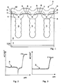
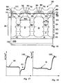
- Such a power MOS device is of the so called multi-drain type and it comprises a heavily doped semiconductor substrate 1, in particular of the N+ type, whereon a semiconductor epitaxial layer 2 of the same N type is formed.
- the epitaxial layer 2 forms a common drain layer for a plurality of elementary units forming the power MOS device 3.
- watch elementary unit comprises a body region 4, in particular of the P type, formed on the epitaxial layer 2.
- each body region 4 there is a column region 5, in particular of the P type, which extends downwards for the whole thickness of the epitaxial layer 2 towards the semiconductor substrate 1.
- each column region 5 is aligned and in contact with a respective body region 4 of an elementary unit of the power MOS device 3.
- the N epitaxial layer 2 of the power MOS device 3 thus formed has a constant resistivity.
- the column regions 5 have a constant concentration along their whole column extension, as shown in figure 3 wherein the concentration of the column regions 5 versus their thickness is illustrated.
- the power MOS device 3 also exhibits, inside the body regions 4, heavily doped source regions 6, in particular of the N type.
- the surface of the epitaxial layer 2 is thus covered with a thin gate oxide layer 7 and with a polysilicon layer 8. Openings are provided in the polysilicon layer 8 and in the thin gate oxide layer 7 to uncover portions of the epitaxial layer 2 surface aligned with each source region 6.
- An insulating layer 9 completely covers the polysilicon layer 8 and it partially covers the source regions 6, so as to allow a source metallic layer 10 to contact the source regions 6 and the body regions 4.
- a drain metallic layer 10A is also provided on the lower surface of the semiconductor substrate.
- the presence of the column regions 5 thus allows to reduce the resistivity of the epitaxial layer 2 without decreasing the breakdown voltage BV of the power MOS device 3 as a whole. With this type of devices it is thus possible to reach a predetermined breakdown voltage BV with a resistivity of the epitaxial layer being lower than that used in conventional MOS devices and, in consequence, to obtain power MOS transistors with reduced output resistance.
- power MOS devices 3 formed by means of a plurality of elementary units provided with column regions 5 exhibit an output resistance, being the breakdown voltage equal, shown by the curve A, lower not only than that of conventional MOS devices, shown by the curve B, but also lower than the so called silicon ideal limit, shown by the curve C.
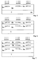
- an epitaxial layer 2 comprising, on the bottom, a first epitaxial layer 2a of the N type with a dopant concentration corresponding to a resistivity p.
- a trench is formed in this second epitaxial layer 2a through the first photolothographic mask for forming a zero level indicator not shown in the figures.
- a second mask is then formed on such first epitaxial layer 2a wherein a plurality of openings are formed.
- a first implant step of P dopant is carried out for forming first implanted regions 5a, as shown in figure 5 .
- a second N epitaxial layer 2b is formed with a dopant concentration corresponding to the resistivity p.
- a third mask is then formed, aligned with the second mask by means of the zero level indicator, on the second epitaxial layer 2b wherein a plurality of openings are formed.
- a second implant step of a P dopant is carried out in the second epitaxial layer 2b for forming second implanted regions 5b.
- a third N epitaxial layer 2c is then formed which has a dopant concentration corresponding to the resistivity p.
- a fourth mask is then formed, aligned with the second, third mask by means of the zero level indicator, on the third epitaxial layer 2c wherein a plurality of openings are formed.
- a third implant step of P dopant is carried out in the third epitaxial layer 2c for forming, by means of a successive diffusion process, third implanted regions 5c.
- the fourth N epitaxial layer 2d is then formed which has a dopant concentration always corresponding to the resistivity p.
- a fifth mask is then formed, aligned with the second, third and fourth by means of the zero level indicator, on the fourth epitaxial layer 2d wherein a plurality of openings are formed.
- a fourth implant step of P dopant in the fourth epitaxial layer 2a is carried out for forming fourth implanted regions 5d.
- a fifth N epitaxial layer 2e is formed having a fifth dopant concentration always corresponding to the resistivity p.
- a sixth mask is then formed, aligned with the second, third and fourth and fifth mask by means of the zero level indicator, on the fifth epitaxial layer 2e wherein a plurality of openings are opened.
- a fifth implant step of P dopant is then carried out in the fifth epitaxial layer 2e for forming the body regions 4 of the power MOS device 3, as shown in figure 1 .
- a seventh mask is then formed, aligned with the second, third and fourth and fifth and sixth mask by means of the zero level indicator, on the fifth epitaxial layer 2e wherein a plurality of openings are formed.
- a sixth implant step of N dopant is then carried out in the fifth epitaxial layer 2e for forming the source regions 6 of the power MOS device 3.
- a diffusion thermal process is then carried out for diffusing the implanted regions 5a, 5b, 5c, 5d, the body regions 4 and the source regions 6 of the power MOS device 3 and so that the implanted regions 5a, 5b, 5c, 5d form a single column region aligned and in contact with the body region 4.
- the process is then completed with the conventional process steps which include the formation of the thin gate oxide layer 7 and the polysilicon layer 8 on the surface of the epitaxial layer 2. Openings are then provided in the polysilicon layer 8 and in the thin gate oxide layer 7 until they uncover portions of the epitaxial layer 2 surface aligned with each source region 6.
- the insulating layer 9 is formed until it completely covers the polysilicon layer and it partially covers the source region 6, so as to allow a source metallic layer 10 formed on the power MOS device 3 to contact the source regions 6 and the body regions 4.
- a drain metallic layer 10A is finally formed on the lower surface of the semiconductor substrate 1.
- the presence of the column regions 5 hooked onto the body regions 4 empties the drain region 2, allowing the power MOS device 3 thus formed to withstand a predetermined voltage applied from the outside to the device even in presence of high concentrations of dopant in the epitaxial layer 2 (which is an conductive layer of the N type, in the case of N channel devices like the one shown with reference to figures 1 and 5-9 ).
- the breakdown voltage BV that the power MOS device 3 thus obtained can withstand, varies, the resistivity of the epitaxial layer 2 being equal, with the dopant concentration in the column regions 5 (which are, in the example shown in figures 1 and 5-9 , of the P type).
- the breakdown voltage BV varies when the P dopant concentration in the drain epitaxial layer 2 increases: in particular, the voltage BV is the highest when the N dopant concentration in the drain epitaxial layer 2 is completely balanced by the P dopant concentration introduced by an implant P dose ⁇ E used for forming the column regions. This condition is indicated as "charge balance”.
- the breakdown voltage BV of the devices obtained is lower than that which is obtained by using the implant dose ⁇ E .
- the resistivity of the epitaxial layer 2 sets the distance between two adjacent column regions 5 and thus the pitch of the whole power MOS device 3 thus formed.
- the lateral extension and the shape of the column regions 5 is in fact univocally determined by the temperature used in the diffusion thermal process for the formation of the column regions 5.
- the breakdown voltage BV the power MOS device 3 must be able to withstand defines the height of the column regions 5: for a device of 500 V it is comprised between 20 and 30 ⁇ m.
- the area occupied by the column regions 5, useful for the cutoff step, is not used during the conduction of the power MOS device 3: the lateral widening from the column regions 5 limits in fact the electrical performances in conduction of the power MOS device 3 thus formed.
- the number of the epitaxial layers forming the drain epitaxial layer 2 and relative implant steps which form P column regions 5 is to be increased.
- the US Patent Application No. 2003/0148559 in the name of Fuji Electric, Co. discloses a vertical MOS including an Varing-conductivity- type drift layer, comprising first and second vertical regions of opposite conductive type alternatively arranged with each other, wherein at least a vertical region is formed by doped regions.
- MDmeshTM innovation technology for high voltage PowerMOSFETs
- XP000985371 discloses a multi drain Mosfet device with a charge balance in the whole thickness of the drain layer. Such charge balance is obtained by p or n-doped columns formed in the drain layer.
- the technical problem underlying the present invention is that of devising a process for manufacturing a multi-drain power electronic device integrated on a semiconductor substrate having such structural characteristics as to allow to obtain devices having low output resistances and contained dimensions (and reduced pitch) overcoming the limits still affecting the devices formed according to the prior art.
- the solution idea underlying the present invention is that of manufacturing a multi-drain power electronic device integrated on a semiconductor substrate comprising P column regions obtained epitaxially as well as N regions delimiting them and obtained by means of implantation. So the column regions exhibit a reduced lateral size.
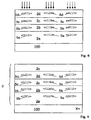
- a first semiconductor layer 21 is formed, for example grown by epitaxy of the N type on the semiconductor substrate 100, having a resistivity ⁇ 1 (for example comprised between 0.5 and 5 ohm*cm) and a first thickness X1 (for example comprised between 2 and 20 ⁇ m).
- a drain semiconductor layer is then formed comprising a second semiconductor layer 22, for example grown by epitaxy of the P type, with a resistivity ⁇ 2 (for example comprised between 0.5 and 2 ohm*cm) and a thickness X2 (for example comprised between 2 and 10 ⁇ m).
- a resistivity ⁇ 2 for example comprised between 0.5 and 2 ohm*cm
- a thickness X2 for example comprised between 2 and 10 ⁇ m.
- a trench is formed in this second semiconductor layer 22 through the first photolithographic mask for forming a zero level indicator not shown in the figures.
- a second mask is formed wherein a plurality of openings are formed. Through these openings a first N dopant implant step is carried out to form, by means of a subsequent diffusion step, first implanted regions D 1.
- the first selective dopant implant step is carried out with a first implant dose ⁇ 1 chosen so that the implanted N dopant concentration balances the P dopant concentration of the second semiconductor layer 22, and the used implant energy is, for example, comprised between 200 and 800 keV, while the first dose ⁇ 1 is, for example comprised between 5x10 11 and 5x10 13 at/cm 2 .
- a third semiconductor layer 23 is formed, for example grown by epitaxy of the P type, with a resistivity ⁇ 3 (for example comprised between 0.5 and 2 ohm*cm) and a thickness X3 (for example comprised between 2 and 10 ⁇ m).
- a third mask is then formed on the third semiconductor layer 23 wherein a plurality of openings are opened.
- such third mask is aligned with the second mask by means of the zero level indicator.
- a second N dopant implant step is then carried out in the third semiconductor layer 23 for forming second implanted regions D2 aligned with the first implanted regions D1.
- the second selective dopant implant step is carried out with a second implant dose ⁇ 2 chosen so that the implanted N dopant concentration balances the P dopant concentration of the third semiconductor layer 23, and an implant energy is used for example comprised between 200 and 800 keV.
- the third semiconductor layer 23 is chosen with a resistivity equal to a resistivity of the second semiconductor layer 22, the second implant dose ⁇ 2 being thus equal to the first implant dose ⁇ 1 .
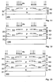
- a fourth semiconductor layer 24 is formed, for example grown by epitaxy of the P type, with a resistivity ⁇ 4 (for example comprised between 0.5 and 2 ohm*cm) and a thickness X4 (for example comprised between 2 and 10 ⁇ m).
- a fourth mask is then formed on the fourth semiconductor layer 24 wherein a plurality of openings are formed.
- such fourth mask is aligned with the previous ones by means of the zero level indicator.
- a third N dopant implant step is then carried out in the fourth semiconductor layer 24 for forming third implanted regions D3 aligned with the second implanted regions D2.
- the third selective dopant implant step is carried out with a third implant dose ⁇ 3 chosen so that the implanted N dopant concentration balances the P dopant concentration of the fourth semiconductor layer 24, and an implant energy is used for example comprised between 200 and 800 keV.
- the fourth semiconductor layer 24 is chosen with a resistivity equal to a resistivity of the third semiconductor layer 23, so that the third implant dose ⁇ 3 is equal to the second implant dose ⁇ 2 .
- a fifth semiconductor layer 25 is formed, for example grown by epitaxy of the P type, with a resistivity ⁇ 2 (for example comprised between 0.5 and 2 ohm*cm) and a thickness X5 (for example comprised between 2 and 10 ⁇ m).
- a fifth mask is then formed on the fifth semiconductor layer 25 wherein a plurality of openings are formed.
- such fifth mask is aligned with the previous ones by means of the zero level indicator.
- a fourth N dopant implant step is then carried out in the fifth semiconductor layer 25 for forming fourth implanted regions D4 aligned with the third implanted regions D3.
- the fourth selective dopant implant step is carried out with a fourth implant dose ⁇ 4 chosen so that the implanted N dopant concentration balances the P dopant concentration of the fifth semiconductor layer 25, and an implant energy is used for example comprised between 200 and 800 keV.
- the fifth semiconductor layer 25 is chosen with a resistivity equal to the resistivity of the fourth semiconductor layer 24, so that the fourth implant dose ⁇ 4 is equal to the third implant dose ⁇ 3 .
- a sixth semiconductor layer 26 is then formed, for example grown by epitaxy of the N type, having a resistivity ⁇ 6 (for example comprised between 0.5 and 5 ohm*cm) and a thickness X6 (for example comprised between 2 and 20 ⁇ m).
- the resistivity ⁇ 6 of the sixth semiconductor layer 26 is equal to that of the first semiconductor layer 21.
- this sixth layer 26 is formed by a P semiconductor layer wherein an N implantation step is carried out, so that the P layer changes completely type.
- a sixth mask is then formed on the sixth semiconductor layer 26 wherein a plurality of openings are formed.
- such openings are formed aligned with the portions of the last P semiconductor layer wherein the implanted regions D1, D2, D3 and D4 have not been formed.
- a fifth P dopant implant step is then carried out for forming body regions 40 of the device 30.
- a seventh mask is then formed on the sixth semiconductor layer 26 wherein a further plurality of openings are formed aligned with the portions of this latter P semiconductor layer wherein the implanted regions D1, D2, D3 and D4 have not been formed.
- a sixth N+ dopant implant step is carried out for forming source regions 60 of the body regions 40, as shown in figure 16 .
- a diffusion thermal process is then carried out for completing the implanted regions D1, D2, D3 and D4, the body regions 40 and the source regions 60 of the device 30 and so that the implanted regions D1, D2, D3 and D4, by diffusing, form a plurality of implanted regions D being electrically continuous of the N column type which extend along the P semiconductor layers and contact the first semiconductor layer 21 and the sixth N semiconductor layer 26.
- N continuous implanted column regions D delimit P column regions 50 which are aligned and in contact with the respective body regions 40.
- the column regions 50 are obtained by overlapping semiconductor layers while the implanted regions D delimiting them are obtained by means of diffusion of implanted regions in the semiconductor layers.
- the semiconductor layer 20 forms a drain layer common by a plurality of elementary units forming the MOS power device.
- Each elementary unit comprises a body region 40 below which there is a column region 50, which, according to the invention, is delimited by pairs of implanted regions D which are obtained by means of diffusion of implanted regions in the semiconductor layers.
- the process for manufacturing the device 30 is then completed with conventional manufacturing steps which include the formation of a thin gate oxide layer 70 and a polysilicon layer 80 on the surface of the drain semiconductor layer 20. Openings are then provided in the polysilicon layer 80 and in the thin gate oxide layer 70 until the portions of the drain semiconductor layer 20 portions are exposed aligned with each source region 60. An insulating layer 90 is formed until it completely covers the polysilicon layer 80 and it partially covers the source regions 60, so as to allow a source metallic layer 110 formed on the device 30 to contact the source regions 60 and the body regions 40. A drain metallic layer 101 is finally formed on the lower surface of the semiconductor substrate 100.
- the concentration profiles both along the N implanted regions D and along the P column regions 50 are substantially flat, as shown in figures 17 and 18 .
- the diffusion thermal process, used to complete the implanted regions D is carried out with a temperature upper than 1150°C, for four hours with a oxygen environment, i.e. high thermal budget thermal process.
- the lateral extension of the P column regions 50 which is a part not used during the conduction of the device 30, is remarkably reduced allowing the scaling (i.e. the pitch reduction, where for pitch is intended the sum of the mead widths of a P column region 50 and a N column region D) of the device itself, in presence of high thermal budget thermal processes and, subsequently, with high thicknesses of the single epitaxial layers 22, 23, , 24 and 25. Therefore, according to the invention, the maximum width W of the P column regions 50 is less than of the maximum width W D of the N column regions D, as shown in figure 16 .
- a power device formed with the method according to the invention in particular having a pitch less or equal to 10 ⁇ m, exhibits a reduced output resistance being the height of the P column regions equal with respect to a device formed according to the prior art.
- the second semiconductor layer 22 has a thickness X2 lower than the thickness X1 of the first semiconductor layer 21.
- the column region 50 is spaced from the semiconductor substrate 100, so that the electric field next to the interface between the semiconductor layer 20 and the semiconductor substrate 100 is reduced.
- An high electric field value in the interface area in fact produces an instability of the device at the breakdown voltage BV.
- drain region 50 made of five epitaxial layers.
- the number of layers used can be different. Such number of semiconductor layers depend in fact on the breakdown voltage BV the final device 30 must withstand.
- the resistivity of the P semiconductor layers 22, 23, 24 and 25 is the same, but advantageously, the resistivity of each single semiconductor forming the drain semiconductor layer 20 is different from that of the adjacent layers so as to form stronger devices.
- a power device 30 manufactured with to the method according to the invention exhibits the following advantages:
Landscapes
- Insulated Gate Type Field-Effect Transistor (AREA)
Claims (14)
- Verfahren zum Herstellen einer leistungselektronischen Vorrichtung (30) mit Mehrfach-Drain, die auf einem Halbleitersubstrat (100) eines ersten Leitfähigkeitstyps integriert ist, wobei das Substrat N+-dotiert ist, wenn es sich bei dem ersten Leitfähigkeitstyp um N-Leitfähigkeit handelt, oder P+-dotiert ist, wenn es sich bei dem ersten Leitfähigkeitstyp um P-Leitfähigkeit handelt,
wobei das Verfahren folgende Schritte aufweist:- durch epitaxiales Wachstum erfolgendes Bilden einer ersten Halbleiterschicht (21) des ersten Leitfähigkeitstyps, die N-dotiert wird, wenn es sich bei dem ersten Leitfähigkeitstyp um N-Leitfähigkeit handelt, oder P-dotiert wird, wenn es sich bei dem ersten Leitfähigkeitstyp um P-Leitfähigkeit handelt, und die einen ersten spezifischen Widerstandswert (p1) auf dem Halbleitersubstrat (100) aufweist,- anschließend durch epitaxiales Wachstum erfolgendes Bilden mindestens einer zweiten Halbleiterschicht (22) eines zweiten Leitfähigkeitstyps und mit einem zweiten spezifischen Widerstandswert (p2) auf der ersten epitaxialen Halbleiterschicht (21),- in der mindestens einen zweiten epitaxialen Halbleiterschicht (22) erfolgendes Bilden einer ersten Mehrzahl von implantierten Bereichen (D1) des ersten Leitfähigkeitstyps mittels eines ersten selektiven Implantierschritts mit einer ersten Implantantierungsdosis (Φ1), die derart gewählt wird, dass ein Ladungsgleichgewicht zwischen der implantierten Dotierstoffkonzentration und der Dotierstoffkonzentration der mindestens einen zweiten epitaxialen Halbleiterschicht (22) vorhanden ist,- über der mindestens einen zweiten epitaxialen Halbleiterschicht (22) erfolgendes Bilden einer Oberflächen-Halbleiterschicht (26) des ersten Leitfähigkeitstyps und mit einem dritten Widerstandswert (p6),- in der Oberflächen-Halbleiterschicht (26) erfolgendes Bilden von Körperbereichen (40) des zweiten Leitfähigkeitstyps, wobei die Körperbereiche (40) mit Bereichen der mindestens einen zweiten epitaxialen Halbleiterschicht (22) ausgerichtet werden, die frei von der ersten Mehrzahl von implantierten Bereichen (D1) sind,- Ausführen eines thermischen Diffusionsschritts, so dass die erste Mehrzahl von implantierten Bereichen (D1) eine Mehrzahl von elektrisch durchgängig implantierten Säulenbereichen (D) in der mindestens einen zweiten epitaxialen Halbleiterschicht (22) bildet, wobei die Mehrzahl der implantierten Säulenbereiche (D) eine Mehrzahl von epitaxialen Säulenbereichen (50) des zweiten Leitfähigkeitstyps begrenzt, die durch die mit den Körperbereichen (40) ausgerichtete mindestens eine zweite epitaxiale Halbleiterschicht (22) gebildet werden, wobei jeder Bereich (50) der Mehrzahl von epitaxialen Säulenbereichen (50) mit einer maximalen Breite (W) ausgebildet wird, die geringer ist als eine maximale Breite (WD) von jedem Bereich (D) der Mehrzahl von implantierten Säulenbereichen (D) und durch die erste Halbleiterschicht (21) begrenzt wird,wobei mit dem thermischen Diffusionsschritt Konzentrationsprofile entlang von jedem der Mehrzahl der implantierten Säulenbereiche (D) und entlang von jedem der Mehrzahl der epitaxialen Säulenbereiche (50) erzielt werden, die im Wesentlichen flach sind. - Verfahren zum Herstellen einer leistungselektronischen Vorrichtung (30) nach Anspruch 1,
wobei das Verfahren folgende Schritte aufweist:- durch epitaxiales Wachstum erfolgendes Bilden einer Mehrzahl von Halbleiterschichten (23, 24, 25) des zweiten Leitfähigkeitstyps auf der mindestens einen zweiten Halbleiterschicht (22),- in jeder Schicht der Mehrzahl von epitaxialen Halbleiterschichten (23, 24, 25) erfolgendes Bilden einer entsprechenden Mehrzahl von implantierten Bereichen (D2, D3, D4) des ersten Leitfähigkeitstyps mittels eines jeweiligen selektiven Implantierschritts mit einer jeweiligen Implantierungsdosis (Φ2, Φ3, Φ4), wobei die jeweilige Mehrzahl von implantierten Bereichen (D2, D3, D4) mit der ersten Mehrzahl von implantierten Bereichen (D1) ausgerichtet wird und während des thermischen Diffusionsschritts die Mehrzahl von implantierten Säulenbereichen (D) in der Mehrzahl der epitaxialen Halbleiterschichten (23, 24, 25) bildet, und wobei jede der Implantierungsdosen (Φ2, Φ3, Φ4), die zum Bilden der jeweiligen Mehrzahl von implantierten Bereichen (D2, D3, D4) angewendet werden, eine Dotierstoffkonzentration der entsprechenden epitaxialen Halbleiterschichten (23, 24, 25) ausgleicht, so dass ein Ladungsgleichgewicht zwischen der Dotierstoffkonzentration von jeder der epitaxialen Halbleiterschichten (23, 24, 25) und der implantierten Dotierstoffkonzentration von jedem der entsprechenden Mehrzahl von implantierten Bereichen (D2, D3, D4) vorhanden ist. - Verfahren zum Herstellen einer leistungselektronischen Vorrichtung (30) nach Anspruch 2,
wobei die Mehrzahl der epitaxialen Halbleiterschichten (22, 23, 24, 25) alle einen gleichen Widerstandswert (p2) aufweisen. - Verfahren zum Herstellen einer leistungselektronischen Vorrichtung (30) nach Anspruch 1,
wobei der erste Widerstandswert (p1) gleich dem dritten Widerstandswert (p6) ist. - Verfahren zum Herstellen einer leistungselektronischen Vorrichtung (30) nach Anspruch 1 oder 2,
wobei die Oberflächen-Halbleiterschicht (26) durch Implantieren eines Dotierstoffs des ersten Leitfähigkeitstyps in einer durch epitaxiales Aufwachsen gebildeten Schicht des zweiten Leitfähigkeitstyps gebildet wird. - Verfahren zum Herstellen einer leistungselektronischen Vorrichtung (30) nach Anspruch 1 oder 2,
wobei die epitaxialen Halbleiterschichten (22; 23, 24, 25) des zweiten Leitfähigkeitstyps aus Schichten gebildet werden, deren Dicke 2 bis 10 µm beträgt. - Verfahren nach Anspruch 1,
wobei die mindestens eine zweite epitaxiale Halbleiterschicht (22) eine geringere Dicke als die erste epitaxiale Halbleiterschicht (21) aufweist. - Verfahren zum Herstellen einer leistungselektronischen Vorrichtung (30) nach Anspruch 1,
wobei die erste epitaxiale Halbleiterschicht (21) des ersten Leitfähigkeitstyps aus einer Schicht gebildet wird, deren Dicke 2 bis 20 µm beträgt. - Verfahren zum Herstellen einer leistungselektronischen Vorrichtung (30) nach Anspruch 7,
wobei die erste epitaxiale Halbleiterschicht (21) des ersten Leitfähigkeitstyps aus einer Schicht gebildet wird, deren spezifischer Widerstand 0,5 bis 5 ohm·cm beträgt. - Verfahren zum Herstellen einer leistungselektronischen Vorrichtung (30) nach Anspruch 1,
wobei der thermische Diffusionsschritt mit einer Temperatur über 1150° C für vier Stunden in einer Sauerstoffumgebung ausgeführt wird. - Leistungselektronische Vorrichtung (30) mit Mehrfach-Drain, die auf einem Halbleitersubstrat (100) eines ersten Leitfähigkeitstyps integriert ist, wobei das Substrat N+-dotiert ist, wenn es sich bei dem ersten Leitfähigkeitstyp um N-Leitfähigkeit handelt, oder P+-dotiert ist, wenn es sich bei dem ersten Leitfähigkeitstyp um P-Leitfähigkeit handelt, und die eine Drain-Halbleiterschicht (20) auf dem Halbleitersubstrat (100) aufweist, wobei die Vorrichtung ferner Folgendes aufweist:- eine erste Halbleiterschicht (21), die N-dotiert ist, wenn es sich bei dem ersten Leitfähigkeitstyp um N-Leitfähigkeit handelt, oder P-dotiert ist, wenn es sich bei dem ersten Leitfähigkeitstyp um P-Leitfähigkeit handelt, auf dem Halbleitersubstrat (100) sowie unter der Drain-Halbleiterschicht (20) und einer zweiten Halbleiter-Oberflächenschicht (26), wobei beide Schichten den ersten Leitfähigkeitstyp aufweisen;- eine Mehrzahl von Körperbereichen (40) eines zweiten Leitfähigkeitstyps, die in der zweiten Halbleiter-Oberflächenschicht (26) gebildet sind,- eine erste Mehrzahl von Säulenbereichen (D) des ersten Leitfähigkeitstyps, die in der Drain-Halbleiterschicht (20) gebildet sind und eine zweite Mehrzahl von Säulenbereichen (50) eines zweiten Leitfähigkeitstyps abgrenzen, wobei jeder Bereich (50) der zweiten Mehrzahl von Säulenbereichen (50) mit einem der Mehrzahl von Körperbereichen (40) ausgerichtet ist,wobei:die Drain-Halbleiterschicht (20) mindestens eine Halbleiterschicht (22, 23, 24, 25) des zweiten Leitfähigkeitstyps aufweist, die mindestens eine Mehrzahl von dotierten Bereichen (D1, D2, D3, D4) des ersten Leitfähigkeitstyps beinhaltet, wobei mindestens die Mehrzahl von dotierten Bereichen (D1, D2, D3, D4) die erste Mehrzahl von Säulenbereichen (D) bildet,wobei jeder Bereich (50) der zweiten Mehrzahl von Säulenbereichen (50) eine maximale Breite (W) aufweist, die geringer ist als eine maximale Breit (WD) jedes Bereichs (D) der ersten Mehrzhal von Säulenbereichen (D) und durch die erste Halbleiterschicht (21) begrenzt ist,wobei sowohl jeder Bereich (D) der ersten Mehrzahl von Säulenbereichen (D) als auch jeder Bereich (50) der zweiten Mehrzahl von Säulenbereichen (50) ein im Wesentlichen flaches Konzentrationsprofil aufweist; undwobei jede der mindestens einen Halbleiterschicht (22, 23, 24, 25) eine derart gewählte Dotierstoffkonzentration aufweist, dass ein Ladungsgleichgewicht mit der Dotierstoffkonzentration der entsprechenden Mehrzahl von dotierten Bereichen (D1, D2, D3, D4) besteht.
- Leistungselektronische Vorrichtung (30) nach Anspruch 11,
dadurch gekennzeichnet, dass die erste Halbleiterschicht (21) und die zweite Halbleiter-Oberflächenschicht (26) den gleichen Dotierstoffkonzentrationswert aufweisen. - Leistungselektronische Vorrichtung (30) nach Anspruch 12,
dadurch gekennzeichnet, dass die erste Halbleiterschicht (21) des ersten Leitfähigkeitstyps eine Dicke aufweist, die 2 bis 20 µm beträgt. - Leistungselektronische Vorrichtung (30) nach Anspruch 12,
dadurch gekennzeichnet, dass die erste Halbleiterschicht (21) des ersten Leitfähigkeitstyps einen spezifischen Widerstand aufweist, der 0,5 bis 5 ohm·cm beträgt.
Priority Applications (1)
| Application Number | Priority Date | Filing Date | Title |
|---|---|---|---|
| EP06762481A EP1908101B1 (de) | 2005-07-08 | 2006-07-07 | Halbleiter-leistungsbauelement mit mehrfach-drain und entsprechender herstellungsprozess |
Applications Claiming Priority (3)
| Application Number | Priority Date | Filing Date | Title |
|---|---|---|---|
| EP05425493A EP1742258A1 (de) | 2005-07-08 | 2005-07-08 | Halbleiter-Leistungsbauelement mit Mehrfach-Drain-Struktur und entsprechendes Herstellungsverfahren |
| PCT/EP2006/006671 WO2007006503A1 (en) | 2005-07-08 | 2006-07-07 | Semiconductor power device with multiple drain and corresponding manufacturing process |
| EP06762481A EP1908101B1 (de) | 2005-07-08 | 2006-07-07 | Halbleiter-leistungsbauelement mit mehrfach-drain und entsprechender herstellungsprozess |
Publications (2)
| Publication Number | Publication Date |
|---|---|
| EP1908101A1 EP1908101A1 (de) | 2008-04-09 |
| EP1908101B1 true EP1908101B1 (de) | 2012-12-26 |
Family
ID=36128597
Family Applications (2)
| Application Number | Title | Priority Date | Filing Date |
|---|---|---|---|
| EP05425493A Withdrawn EP1742258A1 (de) | 2005-07-08 | 2005-07-08 | Halbleiter-Leistungsbauelement mit Mehrfach-Drain-Struktur und entsprechendes Herstellungsverfahren |
| EP06762481A Active EP1908101B1 (de) | 2005-07-08 | 2006-07-07 | Halbleiter-leistungsbauelement mit mehrfach-drain und entsprechender herstellungsprozess |
Family Applications Before (1)
| Application Number | Title | Priority Date | Filing Date |
|---|---|---|---|
| EP05425493A Withdrawn EP1742258A1 (de) | 2005-07-08 | 2005-07-08 | Halbleiter-Leistungsbauelement mit Mehrfach-Drain-Struktur und entsprechendes Herstellungsverfahren |
Country Status (3)
| Country | Link |
|---|---|
| US (2) | US7838927B2 (de) |
| EP (2) | EP1742258A1 (de) |
| WO (1) | WO2007006503A1 (de) |
Families Citing this family (7)
| Publication number | Priority date | Publication date | Assignee | Title |
|---|---|---|---|---|
| IT1397574B1 (it) | 2008-12-29 | 2013-01-16 | St Microelectronics Rousset | Dispositivo a semiconduttore di potenza di tipo multi-drain e relativa struttura di terminazione di bordo |
| US20110049638A1 (en) | 2009-09-01 | 2011-03-03 | Stmicroelectronics S.R.L. | Structure for high voltage device and corresponding integration process |
| CN104254920B (zh) * | 2012-07-19 | 2017-03-08 | 富士电机株式会社 | 半导体装置及半导体装置的制造方法 |
| US10398203B2 (en) * | 2014-02-11 | 2019-09-03 | Ferno-Washington, Inc. | Crash-ready, portable, compartmentalization device |
| US10398207B2 (en) * | 2014-02-11 | 2019-09-03 | Ferno-Washington, Inc. | Crash-ready, portable, compartmentalization device |
| US9306034B2 (en) * | 2014-02-24 | 2016-04-05 | Vanguard International Semiconductor Corporation | Method and apparatus for power device with multiple doped regions |
| CN105977161A (zh) * | 2016-06-21 | 2016-09-28 | 中航(重庆)微电子有限公司 | 超结结构及其制备方法 |
Citations (1)
| Publication number | Priority date | Publication date | Assignee | Title |
|---|---|---|---|---|
| US20030132450A1 (en) * | 2001-02-21 | 2003-07-17 | Tadaharu Minato | Semiconductor device and method of manufacturing the same |
Family Cites Families (4)
| Publication number | Priority date | Publication date | Assignee | Title |
|---|---|---|---|---|
| JP2001119022A (ja) * | 1999-10-20 | 2001-04-27 | Fuji Electric Co Ltd | 半導体装置及びその製造方法 |
| JP4880889B2 (ja) * | 2003-09-09 | 2012-02-22 | セイコーインスツル株式会社 | 半導体装置の製造方法 |
| US7253477B2 (en) * | 2005-02-15 | 2007-08-07 | Semiconductor Components Industries, L.L.C. | Semiconductor device edge termination structure |
| JP2007012858A (ja) * | 2005-06-30 | 2007-01-18 | Toshiba Corp | 半導体素子及びその製造方法 |
-
2005
- 2005-07-08 EP EP05425493A patent/EP1742258A1/de not_active Withdrawn
-
2006
- 2006-07-07 WO PCT/EP2006/006671 patent/WO2007006503A1/en not_active Ceased
- 2006-07-07 EP EP06762481A patent/EP1908101B1/de active Active
-
2008
- 2008-01-08 US US11/971,168 patent/US7838927B2/en active Active
-
2010
- 2010-10-15 US US12/905,623 patent/US20110034010A1/en not_active Abandoned
Patent Citations (1)
| Publication number | Priority date | Publication date | Assignee | Title |
|---|---|---|---|---|
| US20030132450A1 (en) * | 2001-02-21 | 2003-07-17 | Tadaharu Minato | Semiconductor device and method of manufacturing the same |
Also Published As
| Publication number | Publication date |
|---|---|
| EP1742258A1 (de) | 2007-01-10 |
| US20090001460A1 (en) | 2009-01-01 |
| US7838927B2 (en) | 2010-11-23 |
| WO2007006503A1 (en) | 2007-01-18 |
| US20110034010A1 (en) | 2011-02-10 |
| EP1908101A1 (de) | 2008-04-09 |
Similar Documents
| Publication | Publication Date | Title |
|---|---|---|
| EP1851804B1 (de) | Elektronisches leistungsbauelement des mehrfach-drain-typs, integriert auf einem halbleitungssubstrat und relativer herstellungsprozess | |
| US6479352B2 (en) | Method of fabricating high voltage power MOSFET having low on-resistance | |
| US8012832B2 (en) | Process for manufacturing a multi-drain electronic power device integrated in semiconductor substrate and corresponding device | |
| EP1009036B1 (de) | Leistungsbauelement mit MOS-Gate für hohe Spannungen und diesbezügliches Herstellungsverfahren | |
| EP0772242B1 (de) | Leistungsbauteil in MOS-Technologie mit einer einzelnen kritischen Grösse | |
| US20080076223A1 (en) | Semiconductor device and method of fabricating the same | |
| US20010032998A1 (en) | Super-junction semiconductor device and method of manufacturing the same | |
| US20040150039A1 (en) | Trench MOSFET superjunction structure and method to manufacture | |
| US20170229572A1 (en) | Semiconductor device and method of manufacturing same | |
| US8212292B2 (en) | High gain tunable bipolar transistor | |
| US7838927B2 (en) | Process for manufacturing a multi-drain electronic power device integrated in semiconductor substrate and corresponding device | |
| US20070273006A1 (en) | Bipolar method and structure having improved bvceo/rcs trade-off made with depletable collector columns | |
| US20100001362A1 (en) | Edge termination for semiconductor device | |
| KR100779005B1 (ko) | 반도체 장치 및 그 제조 방법 | |
| US7829954B2 (en) | PMOS depletable drain extension made from NMOS dual depletable drain extensions | |
| EP1753022A1 (de) | Halbleiter-Leistungsbauelement mit Mehrfach-Drain-Struktur und entsprechendes Herstellungsverfahren | |
| JP2004349556A (ja) | 半導体素子 | |
| JPH03119733A (ja) | 高耐電圧半導体装置 |
Legal Events
| Date | Code | Title | Description |
|---|---|---|---|
| PUAI | Public reference made under article 153(3) epc to a published international application that has entered the european phase |
Free format text: ORIGINAL CODE: 0009012 |
|
| 17P | Request for examination filed |
Effective date: 20080122 |
|
| AK | Designated contracting states |
Kind code of ref document: A1 Designated state(s): DE FR GB IT |
|
| RBV | Designated contracting states (corrected) |
Designated state(s): DE FR GB IT |
|
| 17Q | First examination report despatched |
Effective date: 20090129 |
|
| RAP1 | Party data changed (applicant data changed or rights of an application transferred) |
Owner name: STMICROELECTRONICS SRL |
|
| RAP1 | Party data changed (applicant data changed or rights of an application transferred) |
Owner name: STMICROELECTRONICS SRL |
|
| GRAJ | Information related to disapproval of communication of intention to grant by the applicant or resumption of examination proceedings by the epo deleted |
Free format text: ORIGINAL CODE: EPIDOSDIGR1 |
|
| GRAP | Despatch of communication of intention to grant a patent |
Free format text: ORIGINAL CODE: EPIDOSNIGR1 |
|
| DAX | Request for extension of the european patent (deleted) | ||
| GRAS | Grant fee paid |
Free format text: ORIGINAL CODE: EPIDOSNIGR3 |
|
| GRAA | (expected) grant |
Free format text: ORIGINAL CODE: 0009210 |
|
| AK | Designated contracting states |
Kind code of ref document: B1 Designated state(s): DE FR GB IT |
|
| REG | Reference to a national code |
Ref country code: GB Ref legal event code: FG4D |
|
| REG | Reference to a national code |
Ref country code: DE Ref legal event code: R096 Ref document number: 602006033850 Country of ref document: DE Effective date: 20130307 |
|
| PLBE | No opposition filed within time limit |
Free format text: ORIGINAL CODE: 0009261 |
|
| STAA | Information on the status of an ep patent application or granted ep patent |
Free format text: STATUS: NO OPPOSITION FILED WITHIN TIME LIMIT |
|
| PGFP | Annual fee paid to national office [announced via postgrant information from national office to epo] |
Ref country code: FR Payment date: 20130722 Year of fee payment: 8 |
|
| 26N | No opposition filed |
Effective date: 20130927 |
|
| PG25 | Lapsed in a contracting state [announced via postgrant information from national office to epo] |
Ref country code: IT Free format text: LAPSE BECAUSE OF FAILURE TO SUBMIT A TRANSLATION OF THE DESCRIPTION OR TO PAY THE FEE WITHIN THE PRESCRIBED TIME-LIMIT Effective date: 20121226 |
|
| REG | Reference to a national code |
Ref country code: DE Ref legal event code: R097 Ref document number: 602006033850 Country of ref document: DE Effective date: 20130927 |
|
| GBPC | Gb: european patent ceased through non-payment of renewal fee |
Effective date: 20130707 |
|
| PG25 | Lapsed in a contracting state [announced via postgrant information from national office to epo] |
Ref country code: GB Free format text: LAPSE BECAUSE OF NON-PAYMENT OF DUE FEES Effective date: 20130707 |
|
| REG | Reference to a national code |
Ref country code: FR Ref legal event code: ST Effective date: 20150331 |
|
| PG25 | Lapsed in a contracting state [announced via postgrant information from national office to epo] |
Ref country code: FR Free format text: LAPSE BECAUSE OF NON-PAYMENT OF DUE FEES Effective date: 20140731 |
|
| REG | Reference to a national code |
Ref country code: DE Ref legal event code: R079 Ref document number: 602006033850 Country of ref document: DE Free format text: PREVIOUS MAIN CLASS: H01L0021336000 Ipc: H10D0030010000 |
|
| PGFP | Annual fee paid to national office [announced via postgrant information from national office to epo] |
Ref country code: DE Payment date: 20250620 Year of fee payment: 20 |