EP1906136B1 - System for clearance measurement and method of operating the same - Google Patents
System for clearance measurement and method of operating the same Download PDFInfo
- Publication number
- EP1906136B1 EP1906136B1 EP07117162A EP07117162A EP1906136B1 EP 1906136 B1 EP1906136 B1 EP 1906136B1 EP 07117162 A EP07117162 A EP 07117162A EP 07117162 A EP07117162 A EP 07117162A EP 1906136 B1 EP1906136 B1 EP 1906136B1
- Authority
- EP
- European Patent Office
- Prior art keywords
- probe
- plasma
- current
- impedance
- sensing system
- Prior art date
- Legal status (The legal status is an assumption and is not a legal conclusion. Google has not performed a legal analysis and makes no representation as to the accuracy of the status listed.)
- Not-in-force
Links
- 238000000034 method Methods 0.000 title claims description 15
- 238000005259 measurement Methods 0.000 title description 3
- 239000000523 sample Substances 0.000 claims description 74
- 238000012360 testing method Methods 0.000 claims description 23
- 238000012545 processing Methods 0.000 claims description 12
- 230000000977 initiatory effect Effects 0.000 claims description 9
- 230000000087 stabilizing effect Effects 0.000 claims description 8
- 239000004020 conductor Substances 0.000 description 38
- 230000005540 biological transmission Effects 0.000 description 9
- 238000004804 winding Methods 0.000 description 6
- 239000003990 capacitor Substances 0.000 description 5
- 238000010586 diagram Methods 0.000 description 4
- 230000002238 attenuated effect Effects 0.000 description 3
- 238000009413 insulation Methods 0.000 description 3
- 238000003754 machining Methods 0.000 description 3
- XEEYBQQBJWHFJM-UHFFFAOYSA-N Iron Chemical compound [Fe] XEEYBQQBJWHFJM-UHFFFAOYSA-N 0.000 description 2
- PXHVJJICTQNCMI-UHFFFAOYSA-N Nickel Chemical compound [Ni] PXHVJJICTQNCMI-UHFFFAOYSA-N 0.000 description 2
- 238000012986 modification Methods 0.000 description 2
- 230000004048 modification Effects 0.000 description 2
- 230000003071 parasitic effect Effects 0.000 description 2
- XAGFODPZIPBFFR-UHFFFAOYSA-N aluminium Chemical compound [Al] XAGFODPZIPBFFR-UHFFFAOYSA-N 0.000 description 1
- 229910052782 aluminium Inorganic materials 0.000 description 1
- 239000000919 ceramic Substances 0.000 description 1
- 239000000470 constituent Substances 0.000 description 1
- 230000007423 decrease Effects 0.000 description 1
- 238000006073 displacement reaction Methods 0.000 description 1
- 230000000694 effects Effects 0.000 description 1
- 229910052742 iron Inorganic materials 0.000 description 1
- 238000004519 manufacturing process Methods 0.000 description 1
- 239000000463 material Substances 0.000 description 1
- 229910052759 nickel Inorganic materials 0.000 description 1
- 238000000926 separation method Methods 0.000 description 1
- WFKWXMTUELFFGS-UHFFFAOYSA-N tungsten Chemical compound [W] WFKWXMTUELFFGS-UHFFFAOYSA-N 0.000 description 1
- 229910052721 tungsten Inorganic materials 0.000 description 1
- 239000010937 tungsten Substances 0.000 description 1
Images

Classifications
-
- G—PHYSICS
- G01—MEASURING; TESTING
- G01B—MEASURING LENGTH, THICKNESS OR SIMILAR LINEAR DIMENSIONS; MEASURING ANGLES; MEASURING AREAS; MEASURING IRREGULARITIES OF SURFACES OR CONTOURS
- G01B7/00—Measuring arrangements characterised by the use of electric or magnetic techniques
- G01B7/14—Measuring arrangements characterised by the use of electric or magnetic techniques for measuring distance or clearance between spaced objects or spaced apertures
-
- F—MECHANICAL ENGINEERING; LIGHTING; HEATING; WEAPONS; BLASTING
- F05—INDEXING SCHEMES RELATING TO ENGINES OR PUMPS IN VARIOUS SUBCLASSES OF CLASSES F01-F04
- F05D—INDEXING SCHEME FOR ASPECTS RELATING TO NON-POSITIVE-DISPLACEMENT MACHINES OR ENGINES, GAS-TURBINES OR JET-PROPULSION PLANTS
- F05D2270/00—Control
- F05D2270/01—Purpose of the control system
- F05D2270/17—Purpose of the control system to control boundary layer
- F05D2270/172—Purpose of the control system to control boundary layer by a plasma generator, e.g. control of ignition
Definitions
- the invention relates generally to probe and sensor systems, and more particularly to a probe for measuring a clearance between two objects.
- a turbine has a number of turbine blades that are disposed adjacent to a shroud.
- the clearance between a turbine blade and the shroud varies depending on the temperature of the turbine blade. For example, the clearance between the shroud and the turbine blade is greatest when the turbine is cold and gradually decreases as the turbine heats up. It is desirable that a gap or clearance between the turbine blade and the shroud be maintained for safe and effective operation of the turbine.
- a sensor may be disposed within the turbine to measure the distance between the turbine blades and the shroud. The distance may be used to direct movement of the shroud to maintain the desired displacement between the shroud and the turbine blades.
- Efficiency of rotating components such as turbines and compressors are also strongly affected by a gap or clearance between a rotating blade and a component casing. In general, minimizing the gap maximizes the efficiency of the components. However, a small amount of clearance is desirable to prevent the rotating blade from hitting the component casing.
- a capacitance probe is employed to measure the distance between two objects. The probe is located on one of the objects and measures a capacitance with respect to the other object for estimating the clearance between the two objects.
- existing devices are expensive and difficult to manufacture, due to the strict requirements necessary for the devices to operate in harsh operating environments.
- US 6,509,744 discloses a method for measuring the distance between a sensor electrode and a workpiece in order to determine the distance between a machining tool and the workpiece.
- a capacitance formed by the sensor electrode and the workpiece is measured, from which their separation is desirable.
- a plasma is formed between the workpiece and the tool which can interfere with the distance measurement. The plasma effect is overcome by selecting a measuring frequency such that the plasma acts virtually as pure ohmic resistance as such is separable from the overall measurement.
- a clearance sensing system is provided as defined in claim 1.
- the system includes a probe separated from a test object by a variable distance d.
- the system also includes an alternating current (AC) source for supplying a current through the probe, wherein the AC source and the probe are configured to generate a controlled plasma channel between a tip of the probe and the test object.
- the system further includes a processing unit configured to determine the variable distance d based on a voltage difference between the tip of the probe and the test object.
- the method includes disposing a probe a variable distance d from the electrically conductive rotating object.
- the method further includes initiating and stabilizing a plasma discharge between a tip of the probe and the electrically conductive rotating object.
- the method further includes measuring at least one of a voltage drop, a current through a plasma formed between the tip of the probe and the electrically conductive rotating object, and an impedance of the probe.
- the method includes determining the distance to the electrically conductive rotating object based upon at least one of the voltage drop, the current and the impedance
- 'plasma discharge' refers to plasma generated at atmospheric pressure and at a radio frequency with a frequency greater than about 1 MHz.
- FIG. 1 is a diagrammatic illustration of a system 10 for initiating and stabilizing plasma.
- the system 10 may also be referred to as a plasma probe 10.
- the plasma probe 10 includes an inner conductor 12 coupled to an alternating current (AC) voltage source 14.
- an outer conductor 16 including multiple windings 18 is arranged around the inner conductor 12.
- the outer conductor 16 is coupled to the AC voltage source 14 at one end and forms a first electrode 20 at an opposite end.
- a second electrode 22 is separated from the first electrode 20 by a gap 24 for initiating a plasma discharge 26.
- the inner conductor 12 includes a conductor cylindrical in shape.
- the inner conductor 12 includes a wire.
- the outer conductor 16 is a solenoid.
- the inner conductor 12 is grounded.
- the outer conductor 16 is grounded through the AC voltage source 14.
- the plasma discharge 26 initiates an atmospheric pressure radio-frequency plasma with a frequency in a range between about 6 MHz and about 7.5 MHz.
- the inner conductor 12 and the outer conductor 16 are configured to step up a voltage supplied by the AC voltage source 14 to initiate the plasma 26 by at least about 20 dB.
- FIG. 2 is an equivalent circuit 30 of the plasma probe 10 in FIG. 1 .
- the inner conductor 12 as referenced in FIG. 1 and the outer conductor 16 as referenced in FIG. 1 are configured as a series LC circuit, wherein L is the inductance of the outer conductor 16 represented by inductor 32 and C s is the capacitance between the inner conductor 12 and the outer conductor 16 represented by capacitor 34.
- the inductor 32 may have a small real value resistance represented by resistor 36. In a particular embodiment, the resistance 36 may vary between about 10 and about 100 ohms.
- the plasma probe 10 as referenced in FIG. 1 acts as a quarter wave transformer with a distributed transmission line 38 through the inner conductor 12 and the outer conductor 16.
- the outer conductor 16 may include a large number of windings 18 as referenced in FIG. 1 so as to increase the inductance per unit length.
- the windings 18 may include a parasitic capacitance 40 between each of the windings 18 and is much smaller than the capacitance 34 denoted by C s . Consequently, the capacitance 40 may be negligible.
- the electrical circuit 30 may also include a leakage resistance 42 of the capacitance 34 and is denoted by G. The leakage resistance 42 may be very small and hence negligible.
- the AC voltage source 14 Prior to the plasma being initiated, the AC voltage source 14 sees an open circuit transmission line as there is no load.
- the equivalent circuit 30 is resonated at a quarter wavelength. Quarter wave resonance occurs when frequency of the source generates a standing wave in the transmission line 38 such that the physical length of the transmission line 38 is a quarter of the wavelength of the standing wave.
- the source 14 sees a short circuit at an end 44 of the transmission line 38 resulting in a load 46.
- the large current generated passes through the inductor 32 and the capacitor 34.
- impedance of the inductor 32 which is given by 2 ⁇ fL wherein f is the frequency of the source 14, is large as both L and f are large.
- voltage drop across the inductor 32 is large resulting in a high voltage at the end 44 of the transmission line 38.
- the high voltage initiates generation of plasma at the load 46.
- the generation of plasma leads to the transmission line 38 being short circuited at the load 46.
- the current driven into the transmission line 38 may have two paths. One of them being through the inductor 32 as described above and the other being through the load 46 bypassing the inductor 32.
- the current gets split into two paths with lesser amount of current flowing through the inductor 32. This results in a lower voltage drop across the inductor 32 that is also the voltage through the generated plasma at the load 46.
- the current going into the plasma is reduced consequently increasing the plasma resistance.
- a very fast negative feedback loop is generated thus stabilizing the generated plasma at load 46.
- the plasma probe 10 plays an important role in initiating the plasma and then stabilizing the voltage to a desirable value so as not to extinguish the plasma and at the same time preventing any possible burn out.
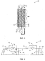
- FIG. 3 depicts a shielded probe system 60 to initiate and stabilize plasma generation.
- the system 60 includes a center conductor 62 coupled at one end to an AC voltage source 64 and forming a first electrode 66 at an opposite end.
- the system 60 also includes an outer conductor 68 including multiple windings 70 arranged around the center conductor 62.
- the outer conductor 68 is coupled at one end to the AC voltage source 64 and form a second electrode 72 at an opposite end.
- the first electrode 66 and the second electrode 72 are separated by a gap 74 to initiate a plasma discharge 76.
- the shielded probe system 60 may initiate a higher temperature plasma discharge than the unshielded probe, warm plasma discharge.
- the system 60 further includes a shield 78 disposed concentric with the center conductor 62 for electromagnetic interference shielding.
- the magnetic field generated by the outer conductor 68 is compressed and exists in the space between the center conductor 62 and the shield 78.
- the center conductor 62 and the outer conductor 68 may be configured to step-up a voltage of the AC voltage source 64 by about 30 dB.
- Insulation 80 may be disposed between the center conductor 62 and the shield 78.
- the insulation 80 may include a ceramic insulation.
- the shield 78 may include an inner conductive cylinder and an outer conductive cylinder that are concentric and connected to one another, and wherein the outer conductor 68 may be disposed between the inner and outer conductive cylinders.
- FIG. 4 is an equivalent circuit 90 of the shielded probe system 60 in FIG. 3 .
- the center conductor 62 in FIG. 3 and the outer conductor 68 in FIG. 3 are configured as a series LC circuit.
- the presence of the shield 78 as referenced in FIG. 3 reduces the effective inductance in the circuit 90 and increases the effective capacitance.
- the effective inductance is equivalent to (L-M) represented by inductor 92, wherein L is the inductance of the center conductor and M is the mutual inductance between the center conductor 62 and the shield 78 due to eddy current losses.
- the effective capacitance is equivalent to (C s1 )+C s2 ) represented by capacitor 94, wherein C s1 is the capacitance between the center conductor 62 and the outer conductor 68 and C s2 is the capacitance between the shield 78 and the outer conductor 68.
- the inductor 92 may have a small real value resistance represented by resistor 96 that includes resistance due to eddy current losses.
- the capacitor 94 may include a negligible leakage resistance represented by a leakage resistor 98.
- the circuit 90 may also include a negligible parasitic capacitance represented by capacitor 100 between each of the windings 70 as referenced in FIG. 3 .
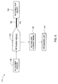
- FIG. 5 is a block diagram representation of a clearance sensing system 110.
- the system 110 includes a probe 112 separated from a test object 114 by a variable distance 116 denoted by 'd'.
- the test object 114 is an electrically conductive rotating test object 114.
- the probe 112 may include a wire made of a material selected from the group consisting of tungsten, iron, nickel and aluminum.
- the probe 112 may be a radio frequency (RF) plasma probe.
- the RF plasma probe may have an operational frequency in a range between about 6 MHz to about 7.5 MHz.
- the RF plasma probe is an unshielded plasma probe as described in FIG. 1 .
- the RF plasma probe is a shielded plasma probe, for example as described in FIG. 3 .
- An alternating (AC) current source 118 is provided for supplying a current to the probe 112.
- the AC source 118 supplies a constant magnitude current to the probe 112.
- a controlled plasma channel 120 may be generated between a tip of the probe 112 and the test object 114.
- the impedance of the plasma channel is primarily resistive and can vary in a range of about one kiliohm and 500 kiliohms depending upon the current flowing through the plasma channel, the channel length and the properties of the gas in the channel (gas constituents, pressure and temperature, for example).
- the plasma is stabilized using a constant current, high frequency (at least about 20 kHz) source 118.
- a voltage and current probe 122 may be used to measure a voltage difference between the tip of the probe 112 and the rotating test object 114.
- the system 110 also includes a processing unit 124 configured to determine the variable distance 'd' 116 based on the voltage difference measured between the tip of the probe 112 and the rotating test object 114. The voltage difference corresponds to a change in impedance of the probe 112. The change in impedance of the probe 112 is proportional to the distance 'd' 116.
- the processing unit 124 is configured to compare the measured change in impedance with calibration data to determine 'd' 116.
- the rotating test object 114 may be part of a turbine or a compressor, for example a turbine blade.
- the variable distance 'd' 116 may be in a range between about 1 ⁇ m to about 20 mm.
- processing unit is intended to denote any machine capable of performing the calculations, or computations, necessary to perform the tasks of the invention.
- processing unit is intended to denote any machine that is capable of accepting a structured input and of processing the input in accordance with prescribed rules to produce an output.
- phrase "configured to” as used herein means that the processing unit is equipped with a combination of hardware and software for performing the tasks of the invention, as will be understood by those skilled in the art.
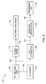
- FIG. 6 is a block diagram representation of a particular example clearance sensing system 110.
- the AC current source comprises a RF carrier source 134.
- a RF signal 132 from a RF carrier source 134 is fed into a RF amplifier 136 that amplifies the RF signal 132.
- the RD amplifier 136 amplifies the RF signal by 50 dB.
- the amplified RF carrier signal 138 is input to a RF plasma probe 112, as referenced in FIG. 5 , to generate and sustain plasma in a gap 116 between the RF plasma probe 112 and the rotating test object 114, as referenced in FIG. 5 .
- the impedance of the plasma channel is primarily resistive and can vary in a range of about one kiliohm and 500 kiliohms depending upon the current flowing through the plasma channel, the channel length and the properties of the gas in the channel.
- the impedance of the load increases. In an example, the impedance may increase from about 50 ohms to about 3 kiliohms.
- the amplified carrier signal 138 from the RF amplifier 136 is fed into an attenuator 140 to reduce the voltage of the amplified RF carrier signal 138 to an attenuated signal level 142 and also to measure voltage without changing the impedance of the generated plasma.
- the attenuator 140 is a high impedance attenuator having an impedance, for example, of about 10 kohm to about 100 kohm.
- the attenuated signal 142 is then input into a demodulator 144 that separates an envelope signal 146 from the attenuated signal 142.
- the envelope signal 146 is separated out.
- the envelope signal 146 is further fed into the processing unit 124 as referenced in FIG. 5 to monitor change in voltage of the envelope signal 146.
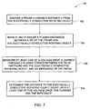
- FIG. 7 is a flow chart illustrating exemplary steps for a method 150 of measuring a distance to an electrically conductive rotating object.
- the method 150 includes disposing a probe at a variable distance d from the electrically conductive rotating object in step 152.
- a plasma discharge between a tip of the probe and the electrically conductive rotating object is initialized and stabilized in step 154.
- the plasma discharge is stabilized by supplying feedback in the probe in order to reduce current through the plasma.
- a voltage drop is measured through the plasma between the tip of the probe and the rotating object is measured in step 156.
- current is measured through the plasma in step 156.
- an impedance is further determined from the measured voltage drop and the current in step 156.
- the complex impedance is equal to the ratio of the measured voltage drop to the constant magnitude current.
- the impedance of the plasma probe is measured. Clearance for the rotating object is determined from at least one of the measured voltage, current and magnitude of the complex impedance in step 158. The determination of the clearance includes comparing the complex impedance with calibration data.
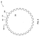
- FIG. 8 is a diagrammatic illustration of a portion of a test rig 160.
- the test rig 160 includes protrusions 162 that may represent turbine blades, for example, and a central portion 164. An optimum distance of clearance between the protrusions 162 and a casing or a shroud (not shown) is to be determined. Further, each of the protrusions 162 includes an edge 166 and a center plateau 168. A bottom plateau 170 denotes an edge of the central portion 164.
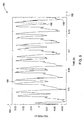
- FIG. 9 is a graphical illustration 180 of the voltage difference measured between a tip of the RF plasma probe 112 as referenced in FIG. 5 and various parts of the rotating test rig 160 in FIG. 8 as a function of time.
- Rotation speed of a tip of the test rig 160 was set to about 0.4 m/sec.
- the X-axis 182 represents the elapsed time in seconds
- the Y-axis 184 represents the voltage of the envelope signal 144 as referenced in FIG. 6 as various parts of the rotating test rig pass the plasma discharge.
- a peak 186 indicates voltage measured at the edge 166 as referenced in FIG. 7 of the turbine blade 162.
- point 188 indicates voltage measured at the center plateau 168 as referenced in FIG.
Landscapes
- Physics & Mathematics (AREA)
- General Physics & Mathematics (AREA)
- Measurement Of Length, Angles, Or The Like Using Electric Or Magnetic Means (AREA)
- Length Measuring Devices With Unspecified Measuring Means (AREA)
- Plasma Technology (AREA)
Description
- The invention relates generally to probe and sensor systems, and more particularly to a probe for measuring a clearance between two objects.
- Various types of probe and sensor systems have been used to measure the distance between two objects. In addition, the probe systems have been used in various applications. For example, a turbine has a number of turbine blades that are disposed adjacent to a shroud. The clearance between a turbine blade and the shroud varies depending on the temperature of the turbine blade. For example, the clearance between the shroud and the turbine blade is greatest when the turbine is cold and gradually decreases as the turbine heats up. It is desirable that a gap or clearance between the turbine blade and the shroud be maintained for safe and effective operation of the turbine. A sensor may be disposed within the turbine to measure the distance between the turbine blades and the shroud. The distance may be used to direct movement of the shroud to maintain the desired displacement between the shroud and the turbine blades.
- Efficiency of rotating components such as turbines and compressors are also strongly affected by a gap or clearance between a rotating blade and a component casing. In general, minimizing the gap maximizes the efficiency of the components. However, a small amount of clearance is desirable to prevent the rotating blade from hitting the component casing. In certain applications, a capacitance probe is employed to measure the distance between two objects. The probe is located on one of the objects and measures a capacitance with respect to the other object for estimating the clearance between the two objects. However, for high temperature applications, such as gas turbines, existing devices are expensive and difficult to manufacture, due to the strict requirements necessary for the devices to operate in harsh operating environments.
-
US 6,509,744 discloses a method for measuring the distance between a sensor electrode and a workpiece in order to determine the distance between a machining tool and the workpiece. A capacitance formed by the sensor electrode and the workpiece is measured, from which their separation is desirable. In some types of machining, e.g. laser machining, a plasma is formed between the workpiece and the tool which can interfere with the distance measurement. The plasma effect is overcome by selecting a measuring frequency such that the plasma acts virtually as pure ohmic resistance as such is separable from the overall measurement. - Therefore, there is a need for an improved sensor system to address the aforementioned issues.
- In accordance with one embodiment of the present invention, a clearance sensing system is provided as defined in claim 1. The system includes a probe separated from a test object by a variable distance d. The system also includes an alternating current (AC) source for supplying a current through the probe, wherein the AC source and the probe are configured to generate a controlled plasma channel between a tip of the probe and the test object. The system further includes a processing unit configured to determine the variable distance d based on a voltage difference between the tip of the probe and the test object.
- In accordance with another embodiment of the invention, there is provided a method of measuring a distance to an electrically conductive rotating object in accordance with claim 8. The method includes disposing a probe a variable distance d from the electrically conductive rotating object. The method further includes initiating and stabilizing a plasma discharge between a tip of the probe and the electrically conductive rotating object. The method further includes measuring at least one of a voltage drop, a current through a plasma formed between the tip of the probe and the electrically conductive rotating object, and an impedance of the probe. In addition, the method includes determining the distance to the electrically conductive rotating object based upon at least one of the voltage drop, the current and the impedance
- These and other features, aspects, and advantages of the present invention will become better understood when the following detailed description of embodiments provided by way of example only is read with reference to the accompanying drawings in which like characters represent like parts throughout the drawings, wherein:
-
FIG. 1 is a diagrammatic illustration of a probe system for initiating and stabilizing plasma at radio frequency in accordance with embodiments of the invention; -
FIG. 2 is an equivalent circuit representing the probe system inFIG. 1 ; -
FIG. 3 is a diagrammatic illustration of a shielded probe system for initiating and stabilizing plasma at radio frequency in accordance with embodiments of the invention; -
FIG. 4 is an equivalent circuit representing the shielded probe system inFIG. 3 ; -
FIG. 5 is a block diagram representation of a clearance sensing system in accordance with embodiments of the invention; -
FIG. 6 is a block diagram representation of a particular example of the clearance sensing system inFIG. 5 ; -
FIG. 7 is a flow chart illustrating exemplary steps for a method of measuring a clearance for a rotating object; -
FIG. 8 is a diagrammatic illustration of a portion of a test rig; and -
FIG. 9 is a graphical illustration of a voltage drop measured between a tip of the probe systems inFIG. 1 andFIG. 3 and a protrusion as inFIG. 8 . - As discussed in detail below, embodiments of the present invention include a clearance sensing system and a method of operating the same. As used herein, 'plasma discharge' refers to plasma generated at atmospheric pressure and at a radio frequency with a frequency greater than about 1 MHz.
- Turning now to the drawings,
FIG. 1 is a diagrammatic illustration of asystem 10 for initiating and stabilizing plasma. Thesystem 10 may also be referred to as aplasma probe 10. Theplasma probe 10 includes aninner conductor 12 coupled to an alternating current (AC)voltage source 14. In the illustrated embodiment, anouter conductor 16 includingmultiple windings 18 is arranged around theinner conductor 12. Theouter conductor 16 is coupled to theAC voltage source 14 at one end and forms afirst electrode 20 at an opposite end. Asecond electrode 22 is separated from thefirst electrode 20 by agap 24 for initiating aplasma discharge 26. In a particular embodiment, theinner conductor 12 includes a conductor cylindrical in shape. In another embodiment, theinner conductor 12 includes a wire. In an example, theouter conductor 16 is a solenoid. In an exemplary embodiment, theinner conductor 12 is grounded. In another embodiment, theouter conductor 16 is grounded through theAC voltage source 14. In an example, theplasma discharge 26 initiates an atmospheric pressure radio-frequency plasma with a frequency in a range between about 6 MHz and about 7.5 MHz. In a particular embodiment, theinner conductor 12 and theouter conductor 16 are configured to step up a voltage supplied by theAC voltage source 14 to initiate theplasma 26 by at least about 20 dB. -
FIG. 2 is anequivalent circuit 30 of theplasma probe 10 inFIG. 1 . For the illustrated embodiment, theinner conductor 12 as referenced inFIG. 1 and theouter conductor 16 as referenced inFIG. 1 are configured as a series LC circuit, wherein L is the inductance of theouter conductor 16 represented byinductor 32 and Cs is the capacitance between theinner conductor 12 and theouter conductor 16 represented bycapacitor 34. Theinductor 32 may have a small real value resistance represented byresistor 36. In a particular embodiment, theresistance 36 may vary between about 10 and about 100 ohms. Theplasma probe 10 as referenced inFIG. 1 acts as a quarter wave transformer with adistributed transmission line 38 through theinner conductor 12 and theouter conductor 16. Theouter conductor 16 may include a large number ofwindings 18 as referenced inFIG. 1 so as to increase the inductance per unit length. Thewindings 18 may include aparasitic capacitance 40 between each of thewindings 18 and is much smaller than thecapacitance 34 denoted by Cs. Consequently, thecapacitance 40 may be negligible. Theelectrical circuit 30 may also include aleakage resistance 42 of thecapacitance 34 and is denoted by G. Theleakage resistance 42 may be very small and hence negligible. - Prior to the plasma being initiated, the
AC voltage source 14 sees an open circuit transmission line as there is no load. Theequivalent circuit 30 is resonated at a quarter wavelength. Quarter wave resonance occurs when frequency of the source generates a standing wave in thetransmission line 38 such that the physical length of thetransmission line 38 is a quarter of the wavelength of the standing wave. Thus, thesource 14 sees a short circuit at anend 44 of thetransmission line 38 resulting in aload 46. This leads to a large amount of current being driven into thetransmission line 38. The large current generated passes through theinductor 32 and thecapacitor 34. Further, impedance of theinductor 32, which is given by 2πfL wherein f is the frequency of thesource 14, is large as both L and f are large. Hence, voltage drop across theinductor 32 is large resulting in a high voltage at theend 44 of thetransmission line 38. The high voltage initiates generation of plasma at theload 46. - The generation of plasma leads to the
transmission line 38 being short circuited at theload 46. In such a scenario, the current driven into thetransmission line 38 may have two paths. One of them being through theinductor 32 as described above and the other being through theload 46 bypassing theinductor 32. Thus, the current gets split into two paths with lesser amount of current flowing through theinductor 32. This results in a lower voltage drop across theinductor 32 that is also the voltage through the generated plasma at theload 46. Hence, the current going into the plasma is reduced consequently increasing the plasma resistance. A very fast negative feedback loop is generated thus stabilizing the generated plasma atload 46. Thus, theplasma probe 10 plays an important role in initiating the plasma and then stabilizing the voltage to a desirable value so as not to extinguish the plasma and at the same time preventing any possible burn out. - In another illustrated embodiment of the invention,
FIG. 3 depicts a shieldedprobe system 60 to initiate and stabilize plasma generation. Thesystem 60 includes acenter conductor 62 coupled at one end to anAC voltage source 64 and forming afirst electrode 66 at an opposite end. Thesystem 60 also includes anouter conductor 68 includingmultiple windings 70 arranged around thecenter conductor 62. For the illustrated embodiment, theouter conductor 68 is coupled at one end to theAC voltage source 64 and form asecond electrode 72 at an opposite end. Thefirst electrode 66 and thesecond electrode 72 are separated by agap 74 to initiate aplasma discharge 76. The shieldedprobe system 60 may initiate a higher temperature plasma discharge than the unshielded probe, warm plasma discharge. Thesystem 60 further includes ashield 78 disposed concentric with thecenter conductor 62 for electromagnetic interference shielding. The magnetic field generated by theouter conductor 68 is compressed and exists in the space between thecenter conductor 62 and theshield 78. Thecenter conductor 62 and theouter conductor 68 may be configured to step-up a voltage of theAC voltage source 64 by about 30 dB.Insulation 80 may be disposed between thecenter conductor 62 and theshield 78. In a particular embodiment, theinsulation 80 may include a ceramic insulation. In an example, theshield 78 may include an inner conductive cylinder and an outer conductive cylinder that are concentric and connected to one another, and wherein theouter conductor 68 may be disposed between the inner and outer conductive cylinders. -
FIG. 4 is anequivalent circuit 90 of the shieldedprobe system 60 inFIG. 3 . For the illustrated embodiment, thecenter conductor 62 inFIG. 3 and theouter conductor 68 inFIG. 3 are configured as a series LC circuit. The presence of theshield 78 as referenced inFIG. 3 reduces the effective inductance in thecircuit 90 and increases the effective capacitance. The effective inductance is equivalent to (L-M) represented byinductor 92, wherein L is the inductance of the center conductor and M is the mutual inductance between thecenter conductor 62 and theshield 78 due to eddy current losses. The effective capacitance is equivalent to (Cs1)+Cs2) represented bycapacitor 94, wherein Cs1 is the capacitance between thecenter conductor 62 and theouter conductor 68 and Cs2 is the capacitance between theshield 78 and theouter conductor 68. Theinductor 92 may have a small real value resistance represented byresistor 96 that includes resistance due to eddy current losses. Thecapacitor 94 may include a negligible leakage resistance represented by aleakage resistor 98. Thecircuit 90 may also include a negligible parasitic capacitance represented bycapacitor 100 between each of thewindings 70 as referenced inFIG. 3 . Since the effective inductance is smaller and there are more losses in the form of eddy currents, the voltage required to initiate a plasma discharge increases. The initiation of a plasma discharge results in a short circuit at anend 102 with aload 104. Hence, this may lead to a lesser efficient plasma probe as compared to the plasma probe described inFIG. 1 . -
FIG. 5 is a block diagram representation of aclearance sensing system 110. Thesystem 110 includes aprobe 112 separated from atest object 114 by avariable distance 116 denoted by 'd'. In particular embodiments, thetest object 114 is an electrically conductiverotating test object 114. In a particular embodiment, theprobe 112 may include a wire made of a material selected from the group consisting of tungsten, iron, nickel and aluminum. In another embodiment, theprobe 112 may be a radio frequency (RF) plasma probe. For example, the RF plasma probe may have an operational frequency in a range between about 6 MHz to about 7.5 MHz. In a particular embodiment, the RF plasma probe is an unshielded plasma probe as described inFIG. 1 . In another embodiment, the RF plasma probe is a shielded plasma probe, for example as described inFIG. 3 . An alternating (AC)current source 118 is provided for supplying a current to theprobe 112. For particular embodiments, theAC source 118 supplies a constant magnitude current to theprobe 112. A controlledplasma channel 120 may be generated between a tip of theprobe 112 and thetest object 114. The impedance of the plasma channel is primarily resistive and can vary in a range of about one kiliohm and 500 kiliohms depending upon the current flowing through the plasma channel, the channel length and the properties of the gas in the channel (gas constituents, pressure and temperature, for example). In certain embodiments, the plasma is stabilized using a constant current, high frequency (at least about 20 kHz)source 118. A voltage andcurrent probe 122 may be used to measure a voltage difference between the tip of theprobe 112 and therotating test object 114. Thesystem 110 also includes aprocessing unit 124 configured to determine the variable distance 'd' 116 based on the voltage difference measured between the tip of theprobe 112 and therotating test object 114. The voltage difference corresponds to a change in impedance of theprobe 112. The change in impedance of theprobe 112 is proportional to the distance 'd' 116. In a particular embodiment, theprocessing unit 124 is configured to compare the measured change in impedance with calibration data to determine 'd' 116. In an example, therotating test object 114 may be part of a turbine or a compressor, for example a turbine blade. In another embodiment, the variable distance 'd' 116 may be in a range between about 1 µm to about 20 mm. - It should be noted that the present invention is not limited to any particular processing unit for performing the processing tasks of the invention. The term "processing unit," as that term is used herein, is intended to denote any machine capable of performing the calculations, or computations, necessary to perform the tasks of the invention. The term "processing unit" is intended to denote any machine that is capable of accepting a structured input and of processing the input in accordance with prescribed rules to produce an output. It should also be noted that the phrase "configured to" as used herein means that the processing unit is equipped with a combination of hardware and software for performing the tasks of the invention, as will be understood by those skilled in the art.
-
FIG. 6 is a block diagram representation of a particular exampleclearance sensing system 110. In the illustrated embodiment, the AC current source comprises aRF carrier source 134. ARF signal 132 from aRF carrier source 134 is fed into aRF amplifier 136 that amplifies theRF signal 132. In the illustrated example, theRD amplifier 136 amplifies the RF signal by 50 dB. The amplifiedRF carrier signal 138 is input to aRF plasma probe 112, as referenced inFIG. 5 , to generate and sustain plasma in agap 116 between theRF plasma probe 112 and therotating test object 114, as referenced inFIG. 5 . As noted above, the impedance of the plasma channel is primarily resistive and can vary in a range of about one kiliohm and 500 kiliohms depending upon the current flowing through the plasma channel, the channel length and the properties of the gas in the channel. Once the plasma is initiated, the impedance of the load increases. In an example, the impedance may increase from about 50 ohms to about 3 kiliohms. The amplified carrier signal 138 from theRF amplifier 136 is fed into anattenuator 140 to reduce the voltage of the amplifiedRF carrier signal 138 to anattenuated signal level 142 and also to measure voltage without changing the impedance of the generated plasma. In the illustrated embodiment, theattenuator 140 is a high impedance attenuator having an impedance, for example, of about 10 kohm to about 100 kohm. Theattenuated signal 142 is then input into ademodulator 144 that separates anenvelope signal 146 from theattenuated signal 142. There are multiple electromagnetic interference signals from various sources at a carrier frequency such as about 7 MHz. In order to avoid the interference signals, theenvelope signal 146 is separated out. Theenvelope signal 146 is further fed into theprocessing unit 124 as referenced inFIG. 5 to monitor change in voltage of theenvelope signal 146. -
FIG. 7 is a flow chart illustrating exemplary steps for amethod 150 of measuring a distance to an electrically conductive rotating object. Themethod 150 includes disposing a probe at a variable distance d from the electrically conductive rotating object instep 152. A plasma discharge between a tip of the probe and the electrically conductive rotating object is initialized and stabilized instep 154. In a particular embodiment, the plasma discharge is stabilized by supplying feedback in the probe in order to reduce current through the plasma. A voltage drop is measured through the plasma between the tip of the probe and the rotating object is measured instep 156. In another embodiment, current is measured through the plasma instep 156. In yet another embodiment, an impedance is further determined from the measured voltage drop and the current instep 156. In general, the complex impedance is equal to the ratio of the measured voltage drop to the constant magnitude current. In yet another embodiment, the impedance of the plasma probe is measured. Clearance for the rotating object is determined from at least one of the measured voltage, current and magnitude of the complex impedance instep 158. The determination of the clearance includes comparing the complex impedance with calibration data. - The examples that follow are merely illustrative and should not be construed to limit the scope of the claimed invention.
-
FIG. 8 is a diagrammatic illustration of a portion of atest rig 160. Thetest rig 160 includesprotrusions 162 that may represent turbine blades, for example, and a central portion 164. An optimum distance of clearance between theprotrusions 162 and a casing or a shroud (not shown) is to be determined. Further, each of theprotrusions 162 includes anedge 166 and acenter plateau 168. Abottom plateau 170 denotes an edge of the central portion 164. -
FIG. 9 is agraphical illustration 180 of the voltage difference measured between a tip of theRF plasma probe 112 as referenced inFIG. 5 and various parts of therotating test rig 160 inFIG. 8 as a function of time. Rotation speed of a tip of thetest rig 160 was set to about 0.4 m/sec. TheX-axis 182 represents the elapsed time in seconds, and the Y-axis 184 represents the voltage of theenvelope signal 144 as referenced inFIG. 6 as various parts of the rotating test rig pass the plasma discharge. Apeak 186 indicates voltage measured at theedge 166 as referenced inFIG. 7 of theturbine blade 162. Similarly,point 188 indicates voltage measured at thecenter plateau 168 as referenced inFIG. 8 of theprotrusion 162 andpoint 190 indicates voltage measured at thebottom plateau 170 as referenced inFIG. 8 between theprotrusions 162. Distance between theedge 166 of theprotrusion 162 and thecenter plateau 168 was about 1.3 mm. Similarly, distance between theedge 166 and thebottom plateau 170 was about 5 mm. As shown, a voltage difference of about 0.04 V was measured between theedge 166 and thecenter plateau 168, while a voltage difference of about 0.055 V was measured between theedge 166 and thebottom plateau 170. - While only certain features of the invention have been illustrated and described herein, many modifications and changes will occur to those skilled in the art. It is, therefore, to be understood that the appended claims are intended to cover all such modifications and changes as fall within their scope of protection.
Claims (10)
- A clearance sensing system (110) comprising:a probe (112) separated from a test object (114) by a variable distance d (116); andan alternating current (AC) source (118) for supplying a current through the probe (112), characterised in that the AC source (118) and the probe (112) are configured to generate a controlled plasma channel (120) between a tip of the probe (112) and the test object (114); anda processing unit (124) is provided which is configured to determine the variable distance d (116) based on a voltage difference through the plasma channel (120) between the tip of the probe (112) and the test object (114).
- The clearance sensing system (110) of claim 1, wherein the probe (112) comprises a radio frequency plasma probe.
- The clearance sensing system (110) of claim 2, wherein the radio frequency plasma probe has an operational frequency greater than about 1 MHz.
- The clearance sensing system (110) of claim 2, further comprising a radio frequency (RF) amplifier (136) configured to receive a RF signal (138) from the AC source (118) and to supply an amplified RF signal to the radio frequency plasma probe.
- The clearance sensing system (110) of any of the preceding claims, wherein the test object (114) comprises a rotating test object.
- The clearance sensing system (110) of any of the preceding claims, further comprising a voltage and current probe (122) configured to measure the voltage difference between the tip of the probe(112) and the rotating test object (114).
- The clearance sensing system (110) of any of the preceding claims, wherein the processing unit (124) is further configured to determine an impedance for the controlled plasma channel (120) and to compare the impedance with a plurality of calibration data to determine the variable distance d (116).
- A method (150) for measuring a distance to an electrically conductive rotating object, the method comprising:disposing (152) a probe at a variable distance d from the electrically conductive rotating object;providing an alternating current (AC) source (118) for supplying a current through the probe (112) and for initiating and stabilizing (154) a controlled plasma channel between a tip of the probe and the electrically conductive rotating object;measuring (156) at least one of a voltage drop, a current through the plasma channel formed between the tip of the probe and the electrically conductive rotating object, and an impedance of the probe; anddetermining (158) the distance to the electrically conductive rotating object based upon at least one of the voltage drop, the current and the impedance.
- The method (150) of claim 8, further comprising supplying feedback in the probe to stabilize the plasma discharge, wherein the initiating and stabilizing (154) comprises maintaining a constant magnitude current through the probe.
- The method (150) of claim 8, wherein determining (158) the distance to the electrically conductive rotating object comprises comparing the impedance with a plurality of calibration data.
Applications Claiming Priority (1)
| Application Number | Priority Date | Filing Date | Title |
|---|---|---|---|
| US11/540,745 US7605595B2 (en) | 2006-09-29 | 2006-09-29 | System for clearance measurement and method of operating the same |
Publications (2)
| Publication Number | Publication Date |
|---|---|
| EP1906136A1 EP1906136A1 (en) | 2008-04-02 |
| EP1906136B1 true EP1906136B1 (en) | 2012-02-08 |
Family
ID=38752513
Family Applications (1)
| Application Number | Title | Priority Date | Filing Date |
|---|---|---|---|
| EP07117162A Not-in-force EP1906136B1 (en) | 2006-09-29 | 2007-09-25 | System for clearance measurement and method of operating the same |
Country Status (7)
| Country | Link |
|---|---|
| US (1) | US7605595B2 (en) |
| EP (1) | EP1906136B1 (en) |
| JP (1) | JP2008089590A (en) |
| CN (1) | CN101153791A (en) |
| BR (1) | BRPI0704921A (en) |
| CA (1) | CA2603372A1 (en) |
| SG (1) | SG141380A1 (en) |
Families Citing this family (23)
| Publication number | Priority date | Publication date | Assignee | Title |
|---|---|---|---|---|
| US7454974B2 (en) * | 2006-09-29 | 2008-11-25 | General Electric Company | Probe system, ultrasound system and method of generating ultrasound |
| US7870719B2 (en) | 2006-10-13 | 2011-01-18 | General Electric Company | Plasma enhanced rapidly expanded gas turbine engine transition duct |
| US7819626B2 (en) | 2006-10-13 | 2010-10-26 | General Electric Company | Plasma blade tip clearance control |
| US7766599B2 (en) | 2006-10-31 | 2010-08-03 | General Electric Company | Plasma lifted boundary layer gas turbine engine vane |
| US7695241B2 (en) | 2006-11-30 | 2010-04-13 | General Electric Company | Downstream plasma shielded film cooling |
| US7588413B2 (en) | 2006-11-30 | 2009-09-15 | General Electric Company | Upstream plasma shielded film cooling |
| US7736123B2 (en) | 2006-12-15 | 2010-06-15 | General Electric Company | Plasma induced virtual turbine airfoil trailing edge extension |
| US7628585B2 (en) | 2006-12-15 | 2009-12-08 | General Electric Company | Airfoil leading edge end wall vortex reducing plasma |
| US8373425B2 (en) * | 2007-04-06 | 2013-02-12 | Hypertherm, Inc. | Plasma insensitive height sensing |
| US7908115B2 (en) * | 2007-10-09 | 2011-03-15 | University Of Notre Dame Du Lac | Plasma sensors and related methods |
| JP5022884B2 (en) * | 2007-12-06 | 2012-09-12 | ゼネラル・エレクトリック・カンパニイ | Probe system, ultrasonic system, and ultrasonic generation method |
| US8317457B2 (en) | 2007-12-28 | 2012-11-27 | General Electric Company | Method of operating a compressor |
| US20100284795A1 (en) * | 2007-12-28 | 2010-11-11 | General Electric Company | Plasma Clearance Controlled Compressor |
| US8282336B2 (en) | 2007-12-28 | 2012-10-09 | General Electric Company | Instability mitigation system |
| US8282337B2 (en) | 2007-12-28 | 2012-10-09 | General Electric Company | Instability mitigation system using stator plasma actuators |
| US20100047055A1 (en) * | 2007-12-28 | 2010-02-25 | Aspi Rustom Wadia | Plasma Enhanced Rotor |
| US8348592B2 (en) | 2007-12-28 | 2013-01-08 | General Electric Company | Instability mitigation system using rotor plasma actuators |
| US7948229B2 (en) * | 2008-08-29 | 2011-05-24 | General Electric Company | High temperature electronics for passive eddy current sensors |
| CN103884467B (en) * | 2014-04-14 | 2016-05-11 | 中国科学院工程热物理研究所 | Plasma pressure probe and utilize the system of its gaging pressure |
| US9709376B2 (en) * | 2014-05-12 | 2017-07-18 | The University Of Akron | High sensitivity inductive sensor for measuring blade tip clearance |
| CN104075888B (en) * | 2014-06-27 | 2016-05-04 | 北京控制工程研究所 | A kind of device and method that utilizes electric noise measurement gear meshing backlass |
| CN112129213B (en) * | 2020-10-26 | 2021-07-27 | 南京航空航天大学 | Tip Clearance Measurement System and Measurement Method Based on Pulse Dielectric Barrier Discharge |
| CN114234771B (en) * | 2021-11-10 | 2023-09-19 | 华能铜川照金煤电有限公司 | Engine air gap measuring device and measuring method |
Family Cites Families (43)
| Publication number | Priority date | Publication date | Assignee | Title |
|---|---|---|---|---|
| US3480963A (en) * | 1965-07-27 | 1969-11-25 | Burroughs Corp | Command responsive multi-channel electrostatic recorder |
| US3711767A (en) * | 1970-10-30 | 1973-01-16 | Wilcom Prod Inc | Method and apparatus for evaluating the integrity of the shield connection in a splicing section joining the ends of adjacent insulated and shielded communication cables |
| US4058765A (en) * | 1976-06-07 | 1977-11-15 | David Richardson | General displacement sensor |
| JPS59166801A (en) * | 1983-03-09 | 1984-09-20 | Nippon Kokan Kk <Nkk> | Differential feedback type vortex distance meter |
| US4845991A (en) * | 1986-12-22 | 1989-07-11 | Combustion Engineering, Inc. | Hydraulic clearance measurement system |
| CA1268851A (en) * | 1987-02-20 | 1990-05-08 | Reginald Montgomery Clements | Method and apparatus for generating underwater acoustics |
| US4806848A (en) * | 1987-03-11 | 1989-02-21 | The United States Of America As Represented By The Secretary Of The Air Force | Compressor blade clearance measurement system |
| US5085499A (en) * | 1988-09-02 | 1992-02-04 | Battelle Memorial Institute | Fiber optics spectrochemical emission sensors |
| US5101165A (en) * | 1990-05-29 | 1992-03-31 | General Electric Company | Electrical capacitance clearanceometer |
| US5365147A (en) * | 1990-11-28 | 1994-11-15 | Nichimen Kabushiki Kaisha | Plasma stabilizing apparatus employing feedback controls |
| US5414345A (en) * | 1991-04-29 | 1995-05-09 | Electronic Development, Inc. | Apparatus and method for low cost electromagnetic field susceptibility testing |
| US6146135A (en) * | 1991-08-19 | 2000-11-14 | Tadahiro Ohmi | Oxide film forming method |
| JPH0719670B2 (en) * | 1991-10-31 | 1995-03-06 | 日本高周波株式会社 | Triple-probe plasma measuring device that corrects space potential error |
| US5800618A (en) * | 1992-11-12 | 1998-09-01 | Ngk Insulators, Ltd. | Plasma-generating electrode device, an electrode-embedded article, and a method of manufacturing thereof |
| US5382911A (en) * | 1993-03-29 | 1995-01-17 | International Business Machines Corporation | Reaction chamber interelectrode gap monitoring by capacitance measurement |
| DE4340395C1 (en) * | 1993-11-26 | 1994-12-15 | Weidmueller Interface | Method for processing a workpiece by means of a laser beam |
| US5723980A (en) * | 1995-06-07 | 1998-03-03 | Aerogage Corporation | Clearance measurement system |
| JP2641092B2 (en) * | 1995-07-31 | 1997-08-13 | 株式会社小松製作所 | Plasma torch stand-off controller |
| US5734268A (en) * | 1996-04-08 | 1998-03-31 | Motorola, Inc. | Calibration and measurment technique and apparatus for same |
| US5770922A (en) * | 1996-07-22 | 1998-06-23 | Eni Technologies, Inc. | Baseband V-I probe |
| JP3122618B2 (en) * | 1996-08-23 | 2001-01-09 | 東京エレクトロン株式会社 | Plasma processing equipment |
| GB2317265A (en) | 1996-09-13 | 1998-03-18 | Aea Technology Plc | Radio frequency plasma generator |
| JP3356043B2 (en) * | 1997-12-26 | 2002-12-09 | 三菱電機株式会社 | Distance detector for laser processing equipment |
| DE19847365C2 (en) | 1998-10-14 | 2002-04-11 | Precitec Kg | Method for monitoring the machining of a workpiece by means of a machining beam emerging from a machining head |
| DE19906442C2 (en) * | 1999-02-16 | 2001-10-18 | Precitec Kg | Method for measuring the distance between a sensor electrode and a workpiece |
| JP3723861B2 (en) * | 1999-10-05 | 2005-12-07 | 株式会社小松製作所 | Plasma arc spot welding apparatus and method |
| JP4710216B2 (en) * | 2002-06-11 | 2011-06-29 | コニカミノルタホールディングス株式会社 | Thin film formation method |
| TW201041455A (en) * | 2002-12-16 | 2010-11-16 | Japan Science & Tech Agency | Plasma generation device, plasma control method, and substrate manufacturing method |
| JP3837531B2 (en) * | 2003-01-10 | 2006-10-25 | 国立大学法人埼玉大学 | Microscope and surface observation method |
| KR100393522B1 (en) * | 2003-01-11 | 2003-08-02 | Ellipso Technology Co Ltd | Device and method for measuring film thickness, making use of improved fast fourier transformation |
| US7015703B2 (en) * | 2003-08-12 | 2006-03-21 | Scientific Systems Research Limited | Radio frequency Langmuir probe |
| US7015414B2 (en) * | 2003-09-30 | 2006-03-21 | Tokyo Electron Limited | Method and apparatus for determining plasma impedance |
| JP2005117151A (en) * | 2003-10-03 | 2005-04-28 | Murata Mfg Co Ltd | Method of manufacturing surface acoustic wave device and surface acoustic wave device |
| US7251195B1 (en) * | 2003-10-23 | 2007-07-31 | United States Of America As Represented By The Secretary Of The Army | Apparatus for generating an acoustic signal |
| JP3768999B2 (en) * | 2003-10-29 | 2006-04-19 | 澄英 池之内 | Plasma processing apparatus and control method thereof |
| US6998832B1 (en) * | 2004-02-26 | 2006-02-14 | Hd Electric Company | High-voltage indicating apparatus and method |
| US7275013B1 (en) * | 2004-09-20 | 2007-09-25 | University Of Notre Dame Duloc | Plasma anemometer and method for using same |
| US7332915B2 (en) * | 2004-09-28 | 2008-02-19 | General Electric Company | Sensor system and method of operating the same |
| US7180305B2 (en) * | 2004-12-14 | 2007-02-20 | General Electric Company | Sensor systems and methods of operation |
| US7722310B2 (en) * | 2004-12-17 | 2010-05-25 | General Electric Company | System and method for measuring clearance between two objects |
| US20060139039A1 (en) * | 2004-12-23 | 2006-06-29 | Dutton David T | Systems and methods for a contactless electrical probe |
| US8591188B2 (en) * | 2005-04-26 | 2013-11-26 | General Electric Company | Displacement sensor system and method of operation |
| US7333913B2 (en) * | 2005-06-27 | 2008-02-19 | General Electric Company | Clearance measurement system and method of operation |
-
2006
- 2006-09-29 US US11/540,745 patent/US7605595B2/en not_active Expired - Fee Related
-
2007
- 2007-09-14 SG SG200708565-7A patent/SG141380A1/en unknown
- 2007-09-20 CA CA002603372A patent/CA2603372A1/en not_active Abandoned
- 2007-09-21 BR BRPI0704921-8A patent/BRPI0704921A/en not_active IP Right Cessation
- 2007-09-21 JP JP2007245124A patent/JP2008089590A/en active Pending
- 2007-09-25 EP EP07117162A patent/EP1906136B1/en not_active Not-in-force
- 2007-09-29 CN CNA2007101532424A patent/CN101153791A/en active Pending
Also Published As
| Publication number | Publication date |
|---|---|
| BRPI0704921A (en) | 2008-05-27 |
| CN101153791A (en) | 2008-04-02 |
| CA2603372A1 (en) | 2008-03-29 |
| US7605595B2 (en) | 2009-10-20 |
| SG141380A1 (en) | 2008-04-28 |
| JP2008089590A (en) | 2008-04-17 |
| US20080079445A1 (en) | 2008-04-03 |
| EP1906136A1 (en) | 2008-04-02 |
Similar Documents
| Publication | Publication Date | Title |
|---|---|---|
| EP1906136A1 (en) | System for clearance measurement and method of operating the same | |
| Amatucci et al. | Plasma response to strongly sheared flow | |
| US8502455B2 (en) | Atmospheric inductively coupled plasma generator | |
| EP2275776A2 (en) | Method and apparatus for measuring turbine blade tip clearance | |
| US20030141821A1 (en) | Plasma processing apparatus and method capable of performing uniform plasma treatment by control of excitation power | |
| JP3167221B2 (en) | Inductively coupled plasma generator | |
| EP2863170B1 (en) | Tip clearance measurement system | |
| EP2221625A1 (en) | Methods and systems for monitoring stator winding vibration | |
| GB2071852A (en) | Capacitance frequency modulation probe for blade tip clearance measurement | |
| CN101243329A (en) | Method for determining the thickness of a thermal barrier coating on at least one blade of a turbomachine, a corresponding thermal barrier coating layer thickness measuring device for carrying out the method, and applications of the method and the thermal barrier coating thickness measuring device | |
| KR102102487B1 (en) | System, method and apparatus for rf power compensation in plasma etch chamber | |
| JP4288308B2 (en) | High voltage plasma generator | |
| US4845422A (en) | Microwave proximity sensor | |
| KR20220008822A (en) | radio frequency generator | |
| JPH03118490A (en) | Magnetic flux measuring sensor | |
| JP2007281205A (en) | Plasma processing equipment | |
| EP0657742A2 (en) | Detection of arcs in power cables | |
| JP2005226650A (en) | Integrated spark detector that supports the gas turbine engine igniter when installed | |
| US7454974B2 (en) | Probe system, ultrasound system and method of generating ultrasound | |
| Vyroubal et al. | Target temperature effect on eddy-current displacement sensing | |
| KR20220065597A (en) | Plasma device with integrated voltage and current sensor, and method for monitoring voltage and current of plasma device | |
| Godyak et al. | Power measurements and coupler optimization in inductive discharges | |
| US7239133B1 (en) | Methods and systems for controlling the temperature stability of an inductor | |
| KR20050024515A (en) | Sensor for Detecting Signal of Radio Frequency and Large Power | |
| WO2013093399A1 (en) | Proximity sensor with conductive protective shield comprising discontinuities such as slits |
Legal Events
| Date | Code | Title | Description |
|---|---|---|---|
| PUAI | Public reference made under article 153(3) epc to a published international application that has entered the european phase |
Free format text: ORIGINAL CODE: 0009012 |
|
| AK | Designated contracting states |
Kind code of ref document: A1 Designated state(s): AT BE BG CH CY CZ DE DK EE ES FI FR GB GR HU IE IS IT LI LT LU LV MC MT NL PL PT RO SE SI SK TR |
|
| AX | Request for extension of the european patent |
Extension state: AL BA HR MK YU |
|
| 17P | Request for examination filed |
Effective date: 20081002 |
|
| 17Q | First examination report despatched |
Effective date: 20081030 |
|
| AKX | Designation fees paid |
Designated state(s): DE FR GB |
|
| GRAP | Despatch of communication of intention to grant a patent |
Free format text: ORIGINAL CODE: EPIDOSNIGR1 |
|
| GRAS | Grant fee paid |
Free format text: ORIGINAL CODE: EPIDOSNIGR3 |
|
| GRAA | (expected) grant |
Free format text: ORIGINAL CODE: 0009210 |
|
| AK | Designated contracting states |
Kind code of ref document: B1 Designated state(s): DE FR GB |
|
| REG | Reference to a national code |
Ref country code: GB Ref legal event code: FG4D |
|
| REG | Reference to a national code |
Ref country code: DE Ref legal event code: R096 Ref document number: 602007020568 Country of ref document: DE Effective date: 20120405 |
|
| PGFP | Annual fee paid to national office [announced via postgrant information from national office to epo] |
Ref country code: GB Payment date: 20120925 Year of fee payment: 6 |
|
| PLBE | No opposition filed within time limit |
Free format text: ORIGINAL CODE: 0009261 |
|
| STAA | Information on the status of an ep patent application or granted ep patent |
Free format text: STATUS: NO OPPOSITION FILED WITHIN TIME LIMIT |
|
| PGFP | Annual fee paid to national office [announced via postgrant information from national office to epo] |
Ref country code: FR Payment date: 20121001 Year of fee payment: 6 |
|
| 26N | No opposition filed |
Effective date: 20121109 |
|
| PGFP | Annual fee paid to national office [announced via postgrant information from national office to epo] |
Ref country code: DE Payment date: 20120927 Year of fee payment: 6 |
|
| REG | Reference to a national code |
Ref country code: DE Ref legal event code: R097 Ref document number: 602007020568 Country of ref document: DE Effective date: 20121109 |
|
| GBPC | Gb: european patent ceased through non-payment of renewal fee |
Effective date: 20130925 |
|
| REG | Reference to a national code |
Ref country code: FR Ref legal event code: ST Effective date: 20140530 |
|
| REG | Reference to a national code |
Ref country code: DE Ref legal event code: R119 Ref document number: 602007020568 Country of ref document: DE Effective date: 20140401 |
|
| PG25 | Lapsed in a contracting state [announced via postgrant information from national office to epo] |
Ref country code: GB Free format text: LAPSE BECAUSE OF NON-PAYMENT OF DUE FEES Effective date: 20130925 |
|
| PG25 | Lapsed in a contracting state [announced via postgrant information from national office to epo] |
Ref country code: FR Free format text: LAPSE BECAUSE OF NON-PAYMENT OF DUE FEES Effective date: 20130930 Ref country code: DE Free format text: LAPSE BECAUSE OF NON-PAYMENT OF DUE FEES Effective date: 20140401 |