EP1903379B1 - Liquid crystal display device - Google Patents
Liquid crystal display device Download PDFInfo
- Publication number
- EP1903379B1 EP1903379B1 EP07017271.3A EP07017271A EP1903379B1 EP 1903379 B1 EP1903379 B1 EP 1903379B1 EP 07017271 A EP07017271 A EP 07017271A EP 1903379 B1 EP1903379 B1 EP 1903379B1
- Authority
- EP
- European Patent Office
- Prior art keywords
- color
- color filter
- liquid crystal
- light
- crystal display
- Prior art date
- Legal status (The legal status is an assumption and is not a legal conclusion. Google has not performed a legal analysis and makes no representation as to the accuracy of the status listed.)
- Expired - Fee Related
Links
Images


Classifications
-
- G—PHYSICS
- G02—OPTICS
- G02F—OPTICAL DEVICES OR ARRANGEMENTS FOR THE CONTROL OF LIGHT BY MODIFICATION OF THE OPTICAL PROPERTIES OF THE MEDIA OF THE ELEMENTS INVOLVED THEREIN; NON-LINEAR OPTICS; FREQUENCY-CHANGING OF LIGHT; OPTICAL LOGIC ELEMENTS; OPTICAL ANALOGUE/DIGITAL CONVERTERS
- G02F1/00—Devices or arrangements for the control of the intensity, colour, phase, polarisation or direction of light arriving from an independent light source, e.g. switching, gating or modulating; Non-linear optics
- G02F1/01—Devices or arrangements for the control of the intensity, colour, phase, polarisation or direction of light arriving from an independent light source, e.g. switching, gating or modulating; Non-linear optics for the control of the intensity, phase, polarisation or colour
- G02F1/13—Devices or arrangements for the control of the intensity, colour, phase, polarisation or direction of light arriving from an independent light source, e.g. switching, gating or modulating; Non-linear optics for the control of the intensity, phase, polarisation or colour based on liquid crystals, e.g. single liquid crystal display cells
- G02F1/133—Constructional arrangements; Operation of liquid crystal cells; Circuit arrangements
- G02F1/1333—Constructional arrangements; Manufacturing methods
- G02F1/1335—Structural association of cells with optical devices, e.g. polarisers or reflectors
- G02F1/133509—Filters, e.g. light shielding masks
- G02F1/133514—Colour filters
-
- G—PHYSICS
- G02—OPTICS
- G02F—OPTICAL DEVICES OR ARRANGEMENTS FOR THE CONTROL OF LIGHT BY MODIFICATION OF THE OPTICAL PROPERTIES OF THE MEDIA OF THE ELEMENTS INVOLVED THEREIN; NON-LINEAR OPTICS; FREQUENCY-CHANGING OF LIGHT; OPTICAL LOGIC ELEMENTS; OPTICAL ANALOGUE/DIGITAL CONVERTERS
- G02F2203/00—Function characteristic
- G02F2203/02—Function characteristic reflective
-
- G—PHYSICS
- G02—OPTICS
- G02F—OPTICAL DEVICES OR ARRANGEMENTS FOR THE CONTROL OF LIGHT BY MODIFICATION OF THE OPTICAL PROPERTIES OF THE MEDIA OF THE ELEMENTS INVOLVED THEREIN; NON-LINEAR OPTICS; FREQUENCY-CHANGING OF LIGHT; OPTICAL LOGIC ELEMENTS; OPTICAL ANALOGUE/DIGITAL CONVERTERS
- G02F2203/00—Function characteristic
- G02F2203/09—Function characteristic transflective
Definitions
- This invention relates to a liquid crystal display device.
- a liquid crystal display device includes two display panels in which an electric field generating electrode such as a pixel electrode and a common electrode are formed with a liquid crystal layer interposed between the two display panels. Voltages applied to the electric field generating electrode apply an electric field to the liquid crystal layer that determines the alignment of the liquid crystal molecules in the liquid crystal layer which controls the polarization of incident light to display an image.
- an electric field generating electrode such as a pixel electrode and a common electrode
- the image is viewed only from one side of the liquid crystal display device.
- a liquid crystal display device for viewing images from both sides by interposing two liquid crystal display panels has been used in various fields.
- US 2005/0110923 A1 relates to a transflective LCD device comprising a colour filter having apertures in the reflective portions.
- the liquid crystal display device may be classified as transmissive type, transflective type, or reflective type. Since the transflective and reflective type liquid crystal display devices utilize reflected light, the path of light to be transmitted and their color saturation is different. For this reason, the color saturation of the transflective type and reflective type liquid crystal display device is different from that of the transmissive type liquid crystal display device, causing a reduction in perceived image quality.
- a liquid crystal display device includes a front light unit including a light source and a liquid crystal display panel that displays images by using light provided from the light source and is formed with color filters having apertures.
- the size of the aperture is changed according to the color distribution of the light provided from the light source. When the color distribution is large, the size of the aperture in the color filter of the corresponding color is large, and the size of the aperture is determined in proportion to the color distribution.
- the size of the aperture for each color of filter is made smaller in the order of the blue color filter, the green color filter, and the red color filter.
- the color saturation among the filters is increased in the order of the blue color filter, the green color filter, and the red color filter in the reflection area.
- Still another embodiment of the present invention provides a liquid crystal display device including a front light unit including a light source; and a liquid crystal display panel that displays images by using light provided from the light source, displays images by reflecting light provided from the light source, and is formed with color filters.
- the aperture of the blue color filter among the color filters is formed so as to be larger than the aperture of the red and green color filters, and the aperture of the green color filter is formed so as to be larger than the aperture of the red color filter.
- the light source is a white LED module using a blue LED and YAG.
- An exemplary embodiment of the present invention provides a liquid crystal display device capable of allowing the color saturation of light reflected from a transflective type liquid crystal display device to be constant.
- a color filter is formed by different conditions in accordance with color tones of the color filter.
- the liquid crystal display device has a liquid crystal display panel including a thin film transistor array panel 100, a color filter array panel 200, a liquid crystal layer 3, and a sealant 310.
- the liquid crystal display device includes a light guiding plate 550 and a light source 510 formed on the liquid crystal display panel. That is, the liquid crystal display device has a front light including the light source 510 and the light guiding plate 550.
- a lower polarizer 12 is attached to a lower surface of the thin film transistor array panel 100.
- an upper polarizer 22 is attached to an upper surface of the color filter array panel 200.
- a lower phase retardation film 15 is located between the thin film transistor array panel 100 and the lower polarizer 12
- an upper phase retardation film 25 is located between the color filter array panel 200 and the upper polarizer 22.
- the light guiding plate 550 is located at an outer side of the upper polarizer 22, and a light source 510 and a reflecting plate 520 are formed at one side of the light guiding plate 550.
- the light source 510 serves to provide light into the liquid crystal display panel, and light emitted from the light source 510 enters into the light guiding plate 550.
- the light source 510 is surrounded by the reflecting plate 520, and the reflecting plate 520 to reflect light into light guiding plate 550.
- Light guiding plate 550 leads light into the liquid crystal display panel. It is preferable to guide light into the liquid crystal display panel in a vertical direction.
- the light source 510, the reflecting plate 520, and the light guiding plate 550 are located at the upper surface of the liquid crystal display panel, thereby providing light into the liquid crystal display panel in a frontal lighting manner.
- the light provided into the liquid crystal display panel passes through color filter 230 and is reflected by reflective electrode 194 back through liquid crystal layer 3 and is emitted from the upper side thereof. Therefore, it is possible to view images at the upper side.
- the light not reflected by electrode 194 passes through a transparent electrode 192 and liquid crystal layer 3 and is emitted from the lower side thereof. Therefore, it is possible to view images at the lower side. For this reason, it is possible to view images at both sides in the liquid crystal display device according to the embodiment of the invention.
- the light source 510 may be used by selecting from (1) white LED module, (2) a red-green phosphor LED module' including red and green phosphors, and (3) three kinds of LED modules (hereinafter, referred to as a 'three-color LED module') including red, green, and blue phosphors.
- the white LED module is an LED module radiating white light from a blue chip LED and a YAG that is yellow phosphor.
- the red-green phosphor LED module is an LED module that improves the red component and green component by adding red and green phosphors on the surface of the white LED module.
- the three-color LED module uses by arranging three kinds of LEDs each radiating light of blue, red, and green.
- FIG. 2 is a layout showing a pixel of a transflective liquid crystal display device according to an embodiment of the invention
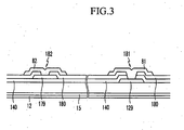
- FIG. 3 and FIG. 4 are cross-sectional views taken along lines III-III and IV-IV of FIG. 2 , respectively.
- the liquid crystal display panel includes a thin film transistor array panel 100, a color filter array panel 200, and a liquid crystal layer 3 interposed between the panels 100 and 200.
- the liquid crystal layer 3 contains liquid crystal molecules aligned vertical or horizontal to surfaces of the panels 100 and 200.
- the thin film transistor array panel 100 is now described in detail.
- a plurality of gate lines 121 and a plurality of storage electrode lines 131 are formed on an insulating substrate 110 made of, for example, a transparent glass or plastic.
- the gate lines 121 transmit gate signals and substantially extend in the transverse direction.
- Each gate line 121 includes a plurality of gate electrodes 124 protruding upwardly and an expanded end 129 provided so as to be connected to another layer or an external driving circuit.
- the storage electrode lines 131 are supplied with a predetermined voltage 131 and substantially extend parallel to the gate lines 121. Each storage electrode line 131 is located between two gate lines 121 adjacent to each other so as to be closer to a lower gate line 121.
- a gate insulating layer 140 made of a silicon nitride (SiNx) or silicon oxide (SiOx) is formed on the gate lines 121 and the storage electrode lines 131.
- a plurality of linear semiconductor layers 151 made of hydrogenated amorphous silicon (hereinafter, the amorphous silicon referred to as "a-Si"), polysilicon or the like are formed on the gate insulating layer 140.
- a plurality of linear-shaped and island-shaped ohmic contacts 161 and 165 are formed on the semiconductor layers 151.
- the linear ohmic contact 161 has a plurality of projections 163, and the projections 163 make pairs with the island-shaped ohmic contact 165.
- the pair of projection 163 and the island-shaped ohmic contact 165 is disposed on the projection 154 of the semiconductor layer 151.
- a plurality of data lines 171 and a plurality of drain electrodes 1 75 are formed on the ohmic contacts 161 and 165 and the gate insulating layer 140.
- the data lines 171 transmit the data voltages and extend in the vertical direction to intersect the gate lines 121 and the storage electrode lines 131.
- Each data line 171 includes a plurality of source electrodes 173 extending toward the gate electrode 124 and the expanded end 179 provided so as to be connected to another layer or an external device.
- the drain electrodes 1 75 are separated from the data lines 171 and face the source electrodes 173 with respect to the gate electrodes 124.
- Each drain electrode 175 has one expanded end and the other end of a bar shape. The expanded end overlaps with the storage electrodes 137, and the bar-shaped end is partially surrounded by the source electrode 1 73.
- One thin film transistor includes one gate electrode 124, one source electrode 1 73, one drain electrode 175, and the projection 154 of the semiconductor layer 151.
- a channel of the thin film transistor is formed at the projection 154 between the source electrode 173 and the drain electrode 175.
- the ohmic contacts 161 and 165 are disposed only between the lower semiconductor layer 151 and the upper data lines 171, thus reducing a contact resistance therebetween.
- the passivation layer 80 includes a lower layer 180q made of the inorganic insulating material such as a silicon nitride and silicon oxide and an upper layer 180p made of an organic insulating material.
- a transmission window 195 is formed on the upper passivation layer 180p. The transmission window 195 exposes a portion of the lower passivation layer 180q.
- the passivation layer 180 may have a single layered structure made of inorganic insulating material or organic insulating materials.
- a plurality of contact holes 182 and 185 for each exposing the end 179 of the data lines 1 71 and the drain electrodes 175 are formed on the passivation layer 180, and a plurality of contact holes 181 for exposing the end 129 of the gate lines 121 are formed on the gate insulating layer 140.
- a plurality of pixel electrodes 191 and a plurality of contact assistant members 81 and 82 are formed on the passivation layer 180.
- Each pixel electrode 191 is formed at the upper surface of the upper passivation layer 180p and includes a transparent electrode 192 and a reflective electrode 194 thereon.
- the transparent electrode 192 is made of a transparent conductive material, such as IZO or ITO
- the reflective electrode 194 is made of a reflective metal, such as aluminum, silver, chrome, or alloy thereof.
- the reflective electrode 194 is located at a transmission window area of the upper passivation layer 1 80p and has a transmission window 195 exposing the transparent electrode 192.
- the reflective electrode 194 is only formed on a part of the transparent electrode 192 so as to expose another part of the transparent electrode 192.
- the exposed part of the transparent electrode 192 is located at the transmission window area of the upper passivation layer 1 80p.
- the pixel electrodes 191 are physically or chemically connected to the drain electrodes 175 through the contact holes 185 such that the data voltages are applied to the pixel electrodes 191 from the drain electrodes 175.
- the pixel electrodes 191 supplied with the data voltages generate electric fields in cooperation with a common electrode 270 of the color filter array panel 200 to which a common voltage is applied, thereby determining the direction of liquid crystal molecules in the liquid crystal layer 3 between two electrodes 191 and 270.
- the transflective type liquid crystal display panel including the thin film transistor array panel 100, the color filter array panel 200, and the liquid crystal layer 3 may be divided into a transmission area TA and a reflection area RA defined by the transparent electrode 192 and the reflective electrode 194. More specifically, the transmission area TA is a section of portions disposed on and under the transmission window 195, and the reflection area RA is a section of portions disposed on and under the reflective electrode 194.
- the transmission areas TA In the transmission areas TA, light entered from the upper surface of the liquid crystal display panel, that is, from color filter array panel 200 is emitted toward the lower surface, that is, the thin transistor array panel 100 by passing through the liquid crystal layer 3, thus displaying images.
- the reflection areas RA light supplied through the upper surface of the LCD panel passes through the LC layer 3, and is then reflected by the reflective electrodes 194. After light is reflected, light passes through the LC layer 3 again and then emits toward the upper surface of the LCD panel, thus displaying images. At this time, light is reflected and dispersed by refraction of the reflective electrode 194.
- the upper passivation layer 1 80p does not exist in the transmission areas TA. Accordingly, the thickness of the LC layer 3 or the cell gap relative to the transmission areas TA is twice as large as the thickness of the LC layer 3 or the cell gap relative to the reflection areas RA.
- the contact assistant members 81 and 82 are connected to the end 129 of the gate lines 121 and the end 1 79 of the data lines 171 through the contact holes 181 and 182, respectively.
- the contact assistant members 81 and 82 complement adhesive property in which the end 129 of the gate lines 121 and the end 179 of the data lines 171 are adhered to the external devices, and prevent the above elements.
- a light blocking member 220 is formed on the insulating substrate 210 made of, for example, the transparent glass or plastic.
- Light blocking members 220 called "black matrix" define aperture regions facing the pixel electrodes 191 and 220 prevent light from leaking out through barriers between the pixel electrodes 191.
- a plurality of color filters 230 are also formed on the substrate 210. Most color filters 230 are disposed within the aperture regions surrounded by the light blocking members 220. The color filters 230 extend along the pixel electrodes 191 in the vertical direction to form a stripe. Each color filter 230 may exhibit one of primary colors such as red, green, and blue colors.
- the color filters 230 are formed at the entire transmission area TA. However, apertures 235 are formed at the reflection area RA. The reason for the apertures 235 is that, in the transmission area TA, light passed through transparent electrode 192 passes through color filter 230 once whereas, in reflection area RA, light passes through color filter 230 twice since it is reflected from the color filter array panel. The size and number of the apertures 235 are changed according to the kinds of light sources and colors of the color filters, as will be described below.
- An overcoat 250 is formed on the color filters 230 and the light blocking member 220, and a common electrode 270 is formed on the overcoat 250.
- the common electrode 270 is preferably made of transparent conductive materials such as ITO and IZO.
- An alignment layer (not shown) is applied to an inner surface of the array panels 100 and 200 so as to align the liquid crystal layer, and polarizers 12 and 22 and phase retardation films 15 and 25 are provided at an outer surface of the array panels 100 and 200, respectively.
- a ⁇ /4 plate or ⁇ /4 plate is preferably used for the phase retardation films 15 and 25, and the ⁇ /4 plate and ⁇ /2 plate may be used together.
- FIG. 5 is a cross-sectional view taken along line III-III of FIG. 2 and is a view different to the embodiment of FIG. 3 .
- FIG. 5 shows a different arrangement of color filters from that of FIG. 4 .
- the color filters used in the reflection area RA and the transmission area TA in one pixel are formed of different substances.
- the color filter 231 of the reflection area RA has less color saturation than the color filter 230 of the transmission area TA. Therefore, if light used in the reflection area RA is twice passed through the color filter 231, the color saturation of the passed light is equal to that of the transmission area TA.
- the color filter 231 of the reflection area RA and the color filter 230 of the transmission area TA may have the same or different thicknesses. For example, color filter 231 in the reflection area RA may be thinner than color filter 230 in the transmission area TA.
- FIG. 5 is substantially the same as that of FIG. 3 .
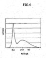
- FIG. 6 is a view showing luminance according to wavelength of light emitted from a white LED module as a light source
- FIG. 7 to FIG. 9 are views showing color filters according to each embodiment of the invention using the light source of FIG. 6 .
- FIG. 6 to FIG. 9 are views showing the embodiments using the white LED module as a light source.
- FIG. 6 shows that the white LED module, which emits white light by using yellow YAG on a blue chip LED, yields the blue light component as the brightest.
- color distribution means the integral value of a dimension of the color filter serving a particular wavelength following the variation of luminance with wavelength.
- the color distribution for the white LED has the order blue > green > red.
- FIG. 7 shows an embodiment where apertures are formed in the color filter.
- FIG. 7 is a view showing briefly only the color filter.
- the color filter is divided into halves in up and down directions, the upper portion is the transmission area TA, and the lower portion is the reflection area RA.
- the reflection area RA includes the apertures 235 so as to adjust the color saturation.
- the blue color filter since the distribution of the blue color is the largest, the blue color filter has the largest apertures 235.
- the distribution of the green color is larger than that of the red color (see FIG. 6 ), the aperture 235 of the green color filter 235 is larger than the aperture 235 of the red color filter.
- the color filter provides no color saturation for the corresponding color in the apertures 235, the color saturation of the corresponding color that is actually transmitted through the color filter is reduced. Accordingly, light passing through the reflection area controls the color saturation of the light source and the color filter so as to have harmonious color saturation.
- FIG. 8 shows an example in which the color filter in the reflection area RA and the transmission area TA is each formed of different substances. That is, the red color filter in the reflection area RA is indicated by reference numeral 231 R, and the red color filter in the transmission area TA is indicated by reference numeral 230R. Moreover, the green and blue color filters in the reflection area RA are indicated by reference numerals 231 G and 231 B, respectively, and the green and blue color filters in the transmission area TA are indicated by reference numeral 230G and 230B, respectively.
- the color filter is formed at the reflection area such that the color saturation increasing ratio by the color filter is reduced in the order of the red color filter 231 R, green color filter 231 G, and blue color filter 231 B.
- light transmitting the reflection area controls the color saturation of the light source and the color filter so as to have a harmonious color saturation.
- FIG. 9 shows an example in which the only blue color filter is formed of two kinds of substances and the red and green color filters are formed with the apertures.
- the color filter is formed at the reflection area such that the color saturation is increased in the order of the red color filter 231 R, green color filter 231 G, and blue color filter 231 B.
- the blue color filter 231 B increases the color saturation slightly by using a separate substance, and the green and red color filters increase the color saturation sufficiently by using the apertures 235G and 2235R. Since the red color filter in the reflection area increases the color saturation as compared to the green color filter in the reflection area, the aperture 235R of the red color filter in the reflection area is formed so as to be smaller than the aperture 235G of the green color filter in the reflection area.
- the blue color filter is formed at the reflection area by using the separate substance, but other colors may also be formed of a separate substance.
- the color filter is formed at the reflection area such that the color saturation is in the order of blue, green, and red.
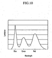
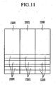
- FIG. 10 is a view showing luminance according to a wavelength of light emitted from LED module where an LED module includes red and green color phosphors as the light source
- FIG. 11 to FIG. 13 are views showing color filters according to each example using the light source of FIG. 10 .
- FIG. 10 to FIG. 13 are views showing an example using a red-green phosphor LED module.
- the red-green phosphor LED module is an LED module that improves the red color component and the green color component by applying the phosphor of the red and green colors on the white LED module.
- FIG. 10 shows the luminance graph according to the wavelength of light emitted from the red-green phosphor LED module.
- the distribution of the blue light is plentiful.
- the distribution of the red light and the green light corresponds to the distribution of the blue light due to the red and green phosphors formed on the surface.
- the difference of the color distribution is within the range of 20%.
- FIG. 11 is a view showing briefly only the color filter.
- the color filter is divided into halves in up and down direction, the upper portion is the transmission area TA, and the lower portion is the reflection area RA.
- the reflection area RA includes the apertures 235 so as to adjust the color saturation.
- the luminance of the blue, green, and red colors harmonize with each other, apertures having the same size are formed, thereby maintaining the balance of the color saturation.
- the size differences of the apertures 235 may be also within the range of 20%.
- FIG. 12 shows an example in which the color filter of the reflection area RA and the transmission area TA is each formed of different substances. That is, the red color filter of the reflection area RA is indicated by reference numeral 231 R, and the red color filter of the transmission area TA is indicated by reference numeral 230R. Moreover, the green and blue color filters of the reflection areas RA are indicated by reference numerals 231 G and 231 B, respectively, and the green and blue color filters of the transmission areas TA are indicated by reference numeral 230G and 230B, respectively.
- the red-green LED module is used in this example, no difference in the distribution of the blue, green, and red colors exists in light provided from the light source. Therefore, the color filter is formed at the reflection area such that the ratio of the color filters providing the color saturation is equal to each other. However, since the difference of the color distribution in the tight source is within the range of 20%, the difference between the color saturation may be within the range of 20%.
- FIG. 13 shows an example in which only the blue color filter is formed of two kinds of substances and apertures are formed in the red and green color filters.
- the color filter is formed at the reflection area such that the ratio of the color saturation is not substantially different among the filters.
- the blue color filter 231 B increases the color saturation by using a separate substance
- the green and red color filters increase the color saturation by using the apertures 235G and 2235R. Since the green color filter and the red color filter in the reflection area increase the color saturation by the same ratio, the size of the aperture 235G in the green reflection area is equal to that of the aperture 235R in the red reflection area.
- the difference of the color distribution in the light source is within the range of 20%
- the difference of the ratio of the color saturation may be within the range of 20% in each color.
- the blue color filter is formed at the reflection area by using a separate substance, but other colors may be used.
- the red-green phosphor LED module is used as a light source even in this case, the color filter is formed at the reflection area such that the ratio of the color saturation is the same in each color. Since the difference of the color distribution in the light source is within the range of 20%, the difference of the ratio of the color saturation may be within the range of 20% in each color.
- the red-green phosphor LED module according to the example was described on the basis of uniformly increasing the color saturation according to the distribution of the blue, green, and red colors.
- the difference in the distribution of the blue, green, and red colors occurs in accordance with the red-green phosphor LED module.
- the color filter in the reflection area having the maximum color distribution is formed so as to slightly increase the color saturation.
- the aperture the largest aperture is formed.
- FIG. 14 is a view showing luminance according to a wavelength of light emitted from LED module in case of using LED module of a red color, a green color, and blue color as a light source
- FIG. 15 is views showing a color filter according to an embodiment of the invention using the light source of FIG. 14 .
- FIG. 14 and FIG. 15 are views showing an example using a three-color LED module.
- the three-color LED module is used by arranging three kinds of LEDs emitting blue light, red light, and green light.
- FIG. 14 shows luminance graph according to the wavelength of light emitted from the three-color LED module. As shown in FIG. 14 , since the three-color LED module uses LED modules exhibiting each color, the three colors have high luminance, and each color has a harmonious distribution.
- FIG. 15 is a view showing briefly only the color filter.
- the color filter is divided into halves in the up and down direction, the upper portion is the transmission area TA, and the lower portion is the reflection area RA.
- the reflection area RA forms the apertures 235 so as to adjust the color saturation.
- the aperture 235 is formed over the reflection area RA. Since each LED module sufficiently exhibits the red color, the blue color, and the green color, the color saturation may be sufficiently exhibited without the color filter. If necessary, the color filter may be formed at a part of the reflection area.
- the apertures When using the three-color LED module, since the blue color, the green color, and the red color have a harmonious distribution, apertures having the same size are formed, thus maintaining the balance of the color saturation. However, since the difference of the color distribution in the three-color LED module is within the range of 20%, the apertures may be formed so as to have the size difference of 20%.
- a color filter having the same structure as used for the red-green phosphor LED module may be used in the reflection area. The reason for this is that the red color, green color, and blue color are balanced with each other in the light source of both the example using the red-green phosphor LED module and the example using the three-color LED module.
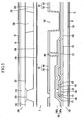
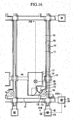
- FIG. 16 is a layout showing a pixel of a reflective type liquid crystal display device according to an example
- FIG. 17 and FIG. 18 are cross-sectional views taken along lines XVII-XVII and XVIII-XVIII of FIG. 16 , respectively.
- the liquid crystal display panel according to the example includes a thin film transistor array panel 100, a color filter array panel 200, and a liquid crystal layer 3 interposed between the panels 100 and 200.
- the liquid crystal layer 3 contains liquid crystal molecules aligned vertical or horizontal to surfaces of the panels 100 and 200.
- the thin film transistor array panel 100 is now described in detail.
- a plurality of gate lines 121 and a plurality of storage electrode lines 131 are formed on an insulating substrate 110 made of, for example, a transparent glass or plastic.
- the gate lines 121 transmit gate signals and substantially extend in the transverse direction.
- the storage electrode lines 131 are supplied with a predetermined voltage 131 and substantially extend parallel to the gate lines 121. Each storage electrode line 131 is located between two gate lines 121 adjacent to each other so as to be closer to a lower gate line 121.
- a gate insulating layer 140 made of a silicon nitride (SiNx) or silicon oxide (SiOx) is formed on the gate lines 121 and the storage electrode lines 131.
- a plurality of linear semiconductor layers 151 made of hydrogenated amorphous silicon (hereinafter, the amorphous silicon referred to as "a-Si"), polysilicon or the like are formed on the gate insulating layer 140.
- a plurality of linear-shaped and island-shaped ohmic contacts 161 and 165 are formed on the semiconductor layers 151.
- the ohmic contacts 161 and 165 may be made of silicide or n+ hydrogenated a-Si heavily doped with n type impurity such as phosphorus.
- a plurality of data lines 171 and a plurality of drain electrodes 1 75 are formed on the ohmic contacts 161 and 165 and the gate insulating layer 140.
- the drain electrodes 175 are separated from the data lines 171 and face the source electrodes 173 with respect to the gate electrodes 124.
- Each drain electrode 175 has one expanded end and the other end of a bar shape. The expanded end overlaps the storage electrodes 137, and the bar-shaped end is partially surrounded by the source electrode 1 73.
- One thin film transistor includes one gate electrode 124, one source electrode 1 73, one drain electrode 175, and the projection 1 54 of the semiconductor layer 151.
- a channel of the thin film transistor is formed at the projection 154 between the source electrode 173 and the drain electrode 175.
- the passivation layer 180 formed on the data lines 171, the drain electrodes 175, and the exposed portions of the semiconductor layer 151.
- the passivation layer 180 includes a lower layer 180q made of the inorganic insulating material such as a silicon nitride and silicon oxide and an upper layer 180p made of an organic insulating material.
- Each reflective electrode 194 is formed at the upper surface of the upper passivation layer 180p and is made of a reflective metal, such as aluminum, silver, chrome, or alloy thereof.
- the reflective electrode 194 covers most of the pixel area to reflect light entered from.
- the reflective electrodes 194 are physically or chemically connected to the drain electrodes 175 through the contact holes 185 to receive the data voltages from the drain electrodes 175.
- the reflective electrodes 194 supplied with the data voltages generate electric fields in cooperation with a common electrode 270 of the color filter array panel 200 to which a common voltage is applied, thereby determining the direction of the liquid crystal molecules in the liquid crystal layer 3 between the two electrodes.
- the reflective type liquid crystal display panel including the thin film transistor array panel 100, the color filter array panel 200, and the liquid crystal layer 3 includes a reflection area RA defined by the reflective electrode 194.
- the reflection areas RA light supplied through the upper surface of the LCD panel passes through the LC layer 3, and is then reflected by the reflective electrodes 194. After light is reflected, light passes through the LC layer 3 again and is then emitted at the upper surface of the LCD panel, thus providing the display. At this time, light is reflected and dispersed by refraction of the reflective electrode 194.
- a light blocking member 220 is formed on the insulating substrate 210 made of, for example, the transparent glass or plastic.
- Light blocking members 220 called "black matrix" define aperture regions facing the reflective electrodes 194 prevent light from leaking out through barriers between the reflective electrodes 194.
- a plurality of color filters 230 are also formed on the substrate 210. Most color filters 230 are disposed within the aperture regions surrounded by the light blocking members 220. The color filters 230 extend along the reflective electrodes 194 in the vertical direction to form a stripe. Each color filter 230 may exhibit one of primary colors such as red, green, and blue colors.
- the reflective type liquid crystal display device passes along twice the color filter 230 when light is entered into the color filter array panel 200 and is reflected from the color filter array panel. This is different to the typical transmissive type liquid crystal display device. Therefore, the color filter different to the color filter of the transmissive type liquid crystal display device may be formed.
- the aperture 235 is formed in the color filter 230 of the reflective type liquid crystal display device.
- the size and number of the apertures 235 are changed by kinds of light sources and colors of the color filters, and it will be described below.
- the color filter may be formed by using a substance having the color saturation different from that of the transmissive type liquid crystal display device without forming the aperture 235.
- An overcoat 250 is formed on the color filters 230 and the light blocking member 220, and a common electrode 270 is formed on the overcoat 250.
- the common electrode 270 is preferably made of transparent conductive materials such as ITO and IZO.
- An alignment layer (not shown) is applied to an inner surface of the array panels 100 and 200 so as to align the liquid crystal layer, and polarizers 12 and 22 and phase retardation films 1 5 and 25 are provided at an outer surface of the array panels 100 and 200, respectively.
- a ⁇ /4 plate or ⁇ /4 plate is preferably used for the phase retardation films 15 and 25, and the ⁇ /4 plate and ⁇ /2 plate may be used together.
- FIG. 19 is views showing color filter according to an example using the light source of FIG. 6
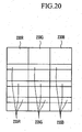
- FIG. 20 is views showing color filter according to an example using the light source of FIG. 10 or FIG. 14 .
- FIG. 19 shows an example using the white LED module as a light source, FIG. 19 and an example forming apertures in the color filter.
- FIG. 19 is a view showing briefly the color filter.
- an entire area of the color filter is the reflection area using light to be reflected.
- the reflection area RA includes the apertures 235 so as to adjust the color saturation.
- the apertures 235 are formed so as to have the largest region within the blue color filter.
- the distribution of the green color is larger than that of the red color (see FIG. 6 ), the aperture 235 is formed such that the aperture 235 of the green color filter 235 is larger than the aperture 235 of the red color filter.
- FIG. 20 shows an example using the red-green phosphor LED module as a light source.
- the example includes the apertures 235 so as to adjust the color saturation.
- the apertures having the same size are formed, thereby maintaining the balance of the color saturation.
- FIG. 20 is applicable to the case using the red-green phosphor LED module and the case using the three-color LED module. However, if the color saturation is sufficiently exhibited by only three-color LED module, the apertures 235 may be formed on the entire pixels. That is, the color filter may be not formed.
- the distribution of each color is harmonious with each other.
- the difference of the color distribution is within the range of 20%
- the difference of the color saturation increasing ratio may be within the range of 20% in each color.
- the color filter is adjusted by the distribution of the colors included in the light source such that the color saturation of images displayed in the reflective mode is constant. As a result, the images are clearly exhibited in the liquid crystal display device, and resolution of the color increases. Moreover, it is possible to increase the display quality without an additional cost.
Description
- This invention relates to a liquid crystal display device.
- A liquid crystal display device includes two display panels in which an electric field generating electrode such as a pixel electrode and a common electrode are formed with a liquid crystal layer interposed between the two display panels. Voltages applied to the electric field generating electrode apply an electric field to the liquid crystal layer that determines the alignment of the liquid crystal molecules in the liquid crystal layer which controls the polarization of incident light to display an image.
- Generally, the image is viewed only from one side of the liquid crystal display device. However, a liquid crystal display device for viewing images from both sides by interposing two liquid crystal display panels has been used in various fields.
-
US 2005/0110923 A1 relates to a transflective LCD device comprising a colour filter having apertures in the reflective portions. - The liquid crystal display device may be classified as transmissive type, transflective type, or reflective type. Since the transflective and reflective type liquid crystal display devices utilize reflected light, the path of light to be transmitted and their color saturation is different. For this reason, the color saturation of the transflective type and reflective type liquid crystal display device is different from that of the transmissive type liquid crystal display device, causing a reduction in perceived image quality.
- In accordance with an aspect of an exemplary embodiment of the invention, a liquid crystal display device includes a front light unit including a light source and a liquid crystal display panel that displays images by using light provided from the light source and is formed with color filters having apertures. According to this embodiment of the invention, the size of the aperture is changed according to the color distribution of the light provided from the light source. When the color distribution is large, the size of the aperture in the color filter of the corresponding color is large, and the size of the aperture is determined in proportion to the color distribution.
- When the light source is a white LED module using a blue color LED and YAG, the size of the aperture for each color of filter is made smaller in the order of the blue color filter, the green color filter, and the red color filter.
- When the light source is a white LED module using a blue LED and YAG, the color saturation among the filters is increased in the order of the blue color filter, the green color filter, and the red color filter in the reflection area.
- Still another embodiment of the present invention provides a liquid crystal display device including a front light unit including a light source; and a liquid crystal display panel that displays images by using light provided from the light source, displays images by reflecting light provided from the light source, and is formed with color filters. According to the embodiment of the invention, the aperture of the blue color filter among the color filters is formed so as to be larger than the aperture of the red and green color filters, and the aperture of the green color filter is formed so as to be larger than the aperture of the red color filter.
- The light source is a white LED module using a blue LED and YAG.
- An exemplary embodiment of the present invention will hereinafter be described in detail with reference to the accompanying drawings, in which:
-
FIG. 1 is a cross-sectional view showing a liquid crystal display device according to an embodiment of the invention. -
FIG. 2 is a layout view showing a pixel of a transflective liquid crystal display device according to an embodiment of the invention. -
FIG. 3 andFIG. 4 are cross-sectional views taken along lines III-III and IV-IV ofFIG. 2 , respectively. -
FIG. 5 is a cross-sectional view taken along line III-III ofFIG. 2 and is a view according to an embodiment of the invention different to that ofFIG. 3 . -
FIG. 6 is a view showing luminance according to a wavelength of light emitted from a white LED module in case of using the white LED module as a light source. -
FIG. 7 is a view showing color filters according to an embodiment of the invention using the light source ofFIG. 6 , respectively. -
Fig. 8 to Fig. 9 are views showing colour filters not forming part of the invention. -
FIG. 10 is a view showing luminance according to a wavelength of light emitted from LED module in case of using LED module including a red color and green color phosphors as a light source. -
FIG. 11 to FIG. 13 are views showing color filters according to an example not forming part of the invention using the light source ofFIG. 10 , respectively. -
FIG. 14 is a view showing luminance according to a wavelength of light emitted from LED module in case of using LED module of a red color, a green color, and blue color as a light source. -
FIG. 15 is views showing color filters according to another example using the light source ofFIG. 14 . -
FIG. 16 is a layout view showing a pixel of a reflective type liquid crystal display device according to a further example. -
FIG. 17 andFIG. 18 are cross-sectional views taken along lines XVII-XVII and XVIII-XVIII ofFIG. 16 , respectively. -
FIG. 19 is views showing color filters according to an example using the light source ofFIG. 6 . -
FIG. 20 is views showing color filters according to an example using the light source ofFIG. 10 orFIG. 14 . - An exemplary embodiment of the present invention provides a liquid crystal display device capable of allowing the color saturation of light reflected from a transflective type liquid crystal display device to be constant.
- In order to achieve the exemplary embodiment of the invention, a color filter is formed by different conditions in accordance with color tones of the color filter.
- In the drawings, the thickness of layers, films, panels, regions, etc., are exaggerated for clarity. Like reference numerals designate like elements throughout the specification. It will be understood that when an element such as a layer, film, region, or substrate is referred to as being "on" another element, it can be directly on the other element or intervening elements may also be present. In contrast, when an element is referred to as being "directly on" another element, there are no intervening elements present.
- As shown in
FIG. 1 , the liquid crystal display device according to the embodiment of the invention has a liquid crystal display panel including a thin filmtransistor array panel 100, a colorfilter array panel 200, aliquid crystal layer 3, and asealant 310. In addition, the liquid crystal display device includes a light guidingplate 550 and alight source 510 formed on the liquid crystal display panel. That is, the liquid crystal display device has a front light including thelight source 510 and thelight guiding plate 550. - More specifically, a
lower polarizer 12 is attached to a lower surface of the thin filmtransistor array panel 100. Meanwhile, anupper polarizer 22 is attached to an upper surface of the colorfilter array panel 200. Even though not shown inFIG. 1 , a lowerphase retardation film 15 is located between the thin filmtransistor array panel 100 and thelower polarizer 12, and an upperphase retardation film 25 is located between the colorfilter array panel 200 and theupper polarizer 22. - The light guiding
plate 550 is located at an outer side of theupper polarizer 22, and alight source 510 and a reflectingplate 520 are formed at one side of thelight guiding plate 550. - The
light source 510 serves to provide light into the liquid crystal display panel, and light emitted from thelight source 510 enters into thelight guiding plate 550. Thelight source 510 is surrounded by thereflecting plate 520, and the reflectingplate 520 to reflect light intolight guiding plate 550. - Light guiding
plate 550 leads light into the liquid crystal display panel. It is preferable to guide light into the liquid crystal display panel in a vertical direction. - As described above, the
light source 510, thereflecting plate 520, and thelight guiding plate 550 are located at the upper surface of the liquid crystal display panel, thereby providing light into the liquid crystal display panel in a frontal lighting manner. - Referring to
Fig. 4 , the light provided into the liquid crystal display panel passes throughcolor filter 230 and is reflected byreflective electrode 194 back throughliquid crystal layer 3 and is emitted from the upper side thereof. Therefore, it is possible to view images at the upper side. - The light not reflected by
electrode 194 passes through atransparent electrode 192 andliquid crystal layer 3 and is emitted from the lower side thereof. Therefore, it is possible to view images at the lower side. For this reason, it is possible to view images at both sides in the liquid crystal display device according to the embodiment of the invention. - Various embodiments may be used as a
light source 510 ofFIG. 1 . Thelight source 510 according to the embodiment of the invention may be used by selecting from (1) white LED module, (2) a red-green phosphor LED module' including red and green phosphors, and (3) three kinds of LED modules (hereinafter, referred to as a 'three-color LED module') including red, green, and blue phosphors. - The white LED module is an LED module radiating white light from a blue chip LED and a YAG that is yellow phosphor. The red-green phosphor LED module is an LED module that improves the red component and green component by adding red and green phosphors on the surface of the white LED module. On the other hand, the three-color LED module uses by arranging three kinds of LEDs each radiating light of blue, red, and green.
- Hereinafter, the transflective type liquid crystal display panel of the liquid crystal display device according to an embodiment of the invention will be described with reference to
FIG. 2 to FIG. 4 . -
FIG. 2 is a layout showing a pixel of a transflective liquid crystal display device according to an embodiment of the invention, andFIG. 3 andFIG. 4 are cross-sectional views taken along lines III-III and IV-IV ofFIG. 2 , respectively. - The liquid crystal display panel according to the embodiment of the invention includes a thin film
transistor array panel 100, a colorfilter array panel 200, and aliquid crystal layer 3 interposed between thepanels liquid crystal layer 3 contains liquid crystal molecules aligned vertical or horizontal to surfaces of thepanels - The thin film
transistor array panel 100 is now described in detail. - A plurality of
gate lines 121 and a plurality ofstorage electrode lines 131 are formed on an insulatingsubstrate 110 made of, for example, a transparent glass or plastic. - The gate lines 121 transmit gate signals and substantially extend in the transverse direction. Each
gate line 121 includes a plurality ofgate electrodes 124 protruding upwardly and an expandedend 129 provided so as to be connected to another layer or an external driving circuit. - The
storage electrode lines 131 are supplied with apredetermined voltage 131 and substantially extend parallel to the gate lines 121. Eachstorage electrode line 131 is located between twogate lines 121 adjacent to each other so as to be closer to alower gate line 121. - A
gate insulating layer 140 made of a silicon nitride (SiNx) or silicon oxide (SiOx) is formed on thegate lines 121 and the storage electrode lines 131. - A plurality of linear semiconductor layers 151 made of hydrogenated amorphous silicon (hereinafter, the amorphous silicon referred to as "a-Si"), polysilicon or the like are formed on the
gate insulating layer 140. - A plurality of linear-shaped and island-shaped
ohmic contacts 161 and 165 are formed on the semiconductor layers 151. The linear ohmic contact 161 has a plurality ofprojections 163, and theprojections 163 make pairs with the island-shapedohmic contact 165. The pair ofprojection 163 and the island-shapedohmic contact 165 is disposed on theprojection 154 of thesemiconductor layer 151. - A plurality of
data lines 171 and a plurality of drain electrodes 1 75 are formed on theohmic contacts 161 and 165 and thegate insulating layer 140. - The data lines 171 transmit the data voltages and extend in the vertical direction to intersect the
gate lines 121 and the storage electrode lines 131. Eachdata line 171 includes a plurality ofsource electrodes 173 extending toward thegate electrode 124 and the expandedend 179 provided so as to be connected to another layer or an external device. - The drain electrodes 1 75 are separated from the
data lines 171 and face thesource electrodes 173 with respect to thegate electrodes 124. Eachdrain electrode 175 has one expanded end and the other end of a bar shape. The expanded end overlaps with thestorage electrodes 137, and the bar-shaped end is partially surrounded by the source electrode 1 73. - One thin film transistor (TFT) includes one
gate electrode 124, one source electrode 1 73, onedrain electrode 175, and theprojection 154 of thesemiconductor layer 151. A channel of the thin film transistor is formed at theprojection 154 between thesource electrode 173 and thedrain electrode 175. - The
ohmic contacts 161 and 165 are disposed only between thelower semiconductor layer 151 and theupper data lines 171, thus reducing a contact resistance therebetween. - A
passivation layer 180 formed on thedata lines 171, thedrain electrodes 175, and the exposed portions of thesemiconductor layer 151. The passivation layer 80 includes alower layer 180q made of the inorganic insulating material such as a silicon nitride and silicon oxide and anupper layer 180p made of an organic insulating material. In addition, atransmission window 195 is formed on theupper passivation layer 180p. Thetransmission window 195 exposes a portion of thelower passivation layer 180q. However, thepassivation layer 180 may have a single layered structure made of inorganic insulating material or organic insulating materials. - A plurality of
contact holes end 179 of the data lines 1 71 and thedrain electrodes 175 are formed on thepassivation layer 180, and a plurality ofcontact holes 181 for exposing theend 129 of thegate lines 121 are formed on thegate insulating layer 140. - A plurality of
pixel electrodes 191 and a plurality ofcontact assistant members passivation layer 180. - Each
pixel electrode 191 is formed at the upper surface of theupper passivation layer 180p and includes atransparent electrode 192 and areflective electrode 194 thereon. Thetransparent electrode 192 is made of a transparent conductive material, such as IZO or ITO, and thereflective electrode 194 is made of a reflective metal, such as aluminum, silver, chrome, or alloy thereof. - The
reflective electrode 194 is located at a transmission window area of the upper passivation layer 1 80p and has atransmission window 195 exposing thetransparent electrode 192. Thereflective electrode 194 is only formed on a part of thetransparent electrode 192 so as to expose another part of thetransparent electrode 192. The exposed part of thetransparent electrode 192 is located at the transmission window area of the upper passivation layer 1 80p. - The
pixel electrodes 191 are physically or chemically connected to thedrain electrodes 175 through the contact holes 185 such that the data voltages are applied to thepixel electrodes 191 from thedrain electrodes 175. Thepixel electrodes 191 supplied with the data voltages generate electric fields in cooperation with acommon electrode 270 of the colorfilter array panel 200 to which a common voltage is applied, thereby determining the direction of liquid crystal molecules in theliquid crystal layer 3 between twoelectrodes - The transflective type liquid crystal display panel including the thin film
transistor array panel 100, the colorfilter array panel 200, and theliquid crystal layer 3 may be divided into a transmission area TA and a reflection area RA defined by thetransparent electrode 192 and thereflective electrode 194. More specifically, the transmission area TA is a section of portions disposed on and under thetransmission window 195, and the reflection area RA is a section of portions disposed on and under thereflective electrode 194. - In the transmission areas TA, light entered from the upper surface of the liquid crystal display panel, that is, from color
filter array panel 200 is emitted toward the lower surface, that is, the thintransistor array panel 100 by passing through theliquid crystal layer 3, thus displaying images. In the reflection areas RA, light supplied through the upper surface of the LCD panel passes through theLC layer 3, and is then reflected by thereflective electrodes 194. After light is reflected, light passes through theLC layer 3 again and then emits toward the upper surface of the LCD panel, thus displaying images. At this time, light is reflected and dispersed by refraction of thereflective electrode 194. - The upper passivation layer 1 80p does not exist in the transmission areas TA. Accordingly, the thickness of the
LC layer 3 or the cell gap relative to the transmission areas TA is twice as large as the thickness of theLC layer 3 or the cell gap relative to the reflection areas RA. - The
contact assistant members end 129 of thegate lines 121 and the end 1 79 of thedata lines 171 through the contact holes 181 and 182, respectively. Thecontact assistant members end 129 of thegate lines 121 and theend 179 of thedata lines 171 are adhered to the external devices, and prevent the above elements. - Hereinafter, the color
filter array panel 200 will be described. - A
light blocking member 220 is formed on the insulatingsubstrate 210 made of, for example, the transparent glass or plastic.Light blocking members 220 called "black matrix" define aperture regions facing thepixel electrodes pixel electrodes 191. - A plurality of
color filters 230 are also formed on thesubstrate 210.Most color filters 230 are disposed within the aperture regions surrounded by thelight blocking members 220. The color filters 230 extend along thepixel electrodes 191 in the vertical direction to form a stripe. Eachcolor filter 230 may exhibit one of primary colors such as red, green, and blue colors. The color filters 230 are formed at the entire transmission area TA. However,apertures 235 are formed at the reflection area RA. The reason for theapertures 235 is that, in the transmission area TA, light passed throughtransparent electrode 192 passes throughcolor filter 230 once whereas, in reflection area RA, light passes throughcolor filter 230 twice since it is reflected from the color filter array panel. The size and number of theapertures 235 are changed according to the kinds of light sources and colors of the color filters, as will be described below. - An
overcoat 250 is formed on thecolor filters 230 and thelight blocking member 220, and acommon electrode 270 is formed on theovercoat 250. Thecommon electrode 270 is preferably made of transparent conductive materials such as ITO and IZO. - An alignment layer (not shown) is applied to an inner surface of the
array panels polarizers phase retardation films array panels phase retardation films -
FIG. 5 is a cross-sectional view taken along line III-III ofFIG. 2 and is a view different to the embodiment ofFIG. 3 . -
FIG. 5 shows a different arrangement of color filters from that ofFIG. 4 . In the embodiment ofFIG. 5 , the color filters used in the reflection area RA and the transmission area TA in one pixel are formed of different substances. Thecolor filter 231 of the reflection area RA has less color saturation than thecolor filter 230 of the transmission area TA. Therefore, if light used in the reflection area RA is twice passed through thecolor filter 231, the color saturation of the passed light is equal to that of the transmission area TA. Thecolor filter 231 of the reflection area RA and thecolor filter 230 of the transmission area TA may have the same or different thicknesses. For example,color filter 231 in the reflection area RA may be thinner thancolor filter 230 in the transmission area TA. - Except for the above-described description, the embodiment of
FIG. 5 is substantially the same as that ofFIG. 3 . - The relationship according to kinds of light sources and the colors of the color filters due to the kinds of light sources will be described with reference t
o FIG. 6 to FIG. 1 5. -
FIG. 6 is a view showing luminance according to wavelength of light emitted from a white LED module as a light source, andFIG. 7 to FIG. 9 are views showing color filters according to each embodiment of the invention using the light source ofFIG. 6 . -
FIG. 6 to FIG. 9 are views showing the embodiments using the white LED module as a light source. -
FIG. 6 , shows that the white LED module, which emits white light by using yellow YAG on a blue chip LED, yields the blue light component as the brightest. - The term color distribution means the integral value of a dimension of the color filter serving a particular wavelength following the variation of luminance with wavelength.
- For example, the color distribution for the white LED, has the order blue > green > red.
-
FIG. 7 shows an embodiment where apertures are formed in the color filter. -
FIG. 7 is a view showing briefly only the color filter. When the color filter is divided into halves in up and down directions, the upper portion is the transmission area TA, and the lower portion is the reflection area RA. As shown inFIG. 7 , the reflection area RA includes theapertures 235 so as to adjust the color saturation. In case of using the white LED module, since the distribution of the blue color is the largest, the blue color filter has thelargest apertures 235. In addition, the distribution of the green color is larger than that of the red color (seeFIG. 6 ), theaperture 235 of thegreen color filter 235 is larger than theaperture 235 of the red color filter. Since the color filter provides no color saturation for the corresponding color in theapertures 235, the color saturation of the corresponding color that is actually transmitted through the color filter is reduced. Accordingly, light passing through the reflection area controls the color saturation of the light source and the color filter so as to have harmonious color saturation. -
FIG. 8 shows an example in which the color filter in the reflection area RA and the transmission area TA is each formed of different substances. That is, the red color filter in the reflection area RA is indicated byreference numeral 231 R, and the red color filter in the transmission area TA is indicated byreference numeral 230R. Moreover, the green and blue color filters in the reflection area RA are indicated byreference numerals reference numeral - Since the white LED module is used in this example, the color distribution of light provided from the light source is reduced in the order of blue color, green color, and red color. Therefore, the color filter is formed at the reflection area such that the color saturation increasing ratio by the color filter is reduced in the order of the
red color filter 231 R,green color filter 231 G, andblue color filter 231 B. As a result, light transmitting the reflection area controls the color saturation of the light source and the color filter so as to have a harmonious color saturation. - Meanwhile,
FIG. 9 shows an example in which the only blue color filter is formed of two kinds of substances and the red and green color filters are formed with the apertures. - Since the white LED module is used in this example, the color distribution of light provided from the light source is reduced in the order of blue color, green color, and red color. Therefore, the color filter is formed at the reflection area such that the color saturation is increased in the order of the
red color filter 231 R,green color filter 231 G, andblue color filter 231 B. However, theblue color filter 231 B increases the color saturation slightly by using a separate substance, and the green and red color filters increase the color saturation sufficiently by using theapertures 235G and 2235R. Since the red color filter in the reflection area increases the color saturation as compared to the green color filter in the reflection area, theaperture 235R of the red color filter in the reflection area is formed so as to be smaller than theaperture 235G of the green color filter in the reflection area. - According to this example, the blue color filter is formed at the reflection area by using the separate substance, but other colors may also be formed of a separate substance. However, since the white LED module is used even in this case, the color filter is formed at the reflection area such that the color saturation is in the order of blue, green, and red.
-
FIG. 10 is a view showing luminance according to a wavelength of light emitted from LED module where an LED module includes red and green color phosphors as the light source, andFIG. 11 to FIG. 13 are views showing color filters according to each example using the light source ofFIG. 10 . -
FIG. 10 to FIG. 13 are views showing an example using a red-green phosphor LED module. As described above, the red-green phosphor LED module is an LED module that improves the red color component and the green color component by applying the phosphor of the red and green colors on the white LED module. -
FIG. 10 shows the luminance graph according to the wavelength of light emitted from the red-green phosphor LED module. As shown inFIG. 10 , the distribution of the blue light is plentiful. In addition, the distribution of the red light and the green light corresponds to the distribution of the blue light due to the red and green phosphors formed on the surface. Generally, in case of the red-green phosphor LED module, the difference of the color distribution is within the range of 20%. -
FIG. 11 is a view showing briefly only the color filter. When the color filter is divided into halves in up and down direction, the upper portion is the transmission area TA, and the lower portion is the reflection area RA. As shown inFIG. 11 , the reflection area RA includes theapertures 235 so as to adjust the color saturation. In case of using the red-green phosphor LED module, since the luminance of the blue, green, and red colors harmonize with each other, apertures having the same size are formed, thereby maintaining the balance of the color saturation. However, since the difference of the color distribution in the light source is within the range of 20%, the size differences of theapertures 235 may be also within the range of 20%. -
FIG. 12 shows an example in which the color filter of the reflection area RA and the transmission area TA is each formed of different substances. That is, the red color filter of the reflection area RA is indicated byreference numeral 231 R, and the red color filter of the transmission area TA is indicated byreference numeral 230R. Moreover, the green and blue color filters of the reflection areas RA are indicated byreference numerals reference numeral - Since the red-green LED module is used in this example, no difference in the distribution of the blue, green, and red colors exists in light provided from the light source. Therefore, the color filter is formed at the reflection area such that the ratio of the color filters providing the color saturation is equal to each other. However, since the difference of the color distribution in the tight source is within the range of 20%, the difference between the color saturation may be within the range of 20%.
-
FIG. 13 shows an example in which only the blue color filter is formed of two kinds of substances and apertures are formed in the red and green color filters. - Since the red-green LED module is used in this example, the difference in the distribution of the blue, green, and red colors is small in the light provided from the light source. Therefore, the color filter is formed at the reflection area such that the ratio of the color saturation is not substantially different among the filters. However, the
blue color filter 231 B increases the color saturation by using a separate substance, and the green and red color filters increase the color saturation by using theapertures 235G and 2235R. Since the green color filter and the red color filter in the reflection area increase the color saturation by the same ratio, the size of theaperture 235G in the green reflection area is equal to that of theaperture 235R in the red reflection area. However, since the difference of the color distribution in the light source is within the range of 20%, the difference of the ratio of the color saturation may be within the range of 20% in each color. - According to this example, the blue color filter is formed at the reflection area by using a separate substance, but other colors may be used. However, since the red-green phosphor LED module is used as a light source even in this case, the color filter is formed at the reflection area such that the ratio of the color saturation is the same in each color. Since the difference of the color distribution in the light source is within the range of 20%, the difference of the ratio of the color saturation may be within the range of 20% in each color.
- The red-green phosphor LED module according to the example was described on the basis of uniformly increasing the color saturation according to the distribution of the blue, green, and red colors. However, the difference in the distribution of the blue, green, and red colors occurs in accordance with the red-green phosphor LED module. In case the difference occurs, the color filter in the reflection area having the maximum color distribution is formed so as to slightly increase the color saturation. At this time, in case of forming the aperture, the largest aperture is formed.
-
FIG. 14 is a view showing luminance according to a wavelength of light emitted from LED module in case of using LED module of a red color, a green color, and blue color as a light source, andFIG. 15 is views showing a color filter according to an embodiment of the invention using the light source ofFIG. 14 . -
FIG. 14 andFIG. 15 are views showing an example using a three-color LED module. As described above, the three-color LED module is used by arranging three kinds of LEDs emitting blue light, red light, and green light. -
FIG. 14 shows luminance graph according to the wavelength of light emitted from the three-color LED module. As shown inFIG. 14 , since the three-color LED module uses LED modules exhibiting each color, the three colors have high luminance, and each color has a harmonious distribution. -
FIG. 15 is a view showing briefly only the color filter. When the color filter is divided into halves in the up and down direction, the upper portion is the transmission area TA, and the lower portion is the reflection area RA. As shown inFIG. 15 , the reflection area RA forms theapertures 235 so as to adjust the color saturation. Theaperture 235 is formed over the reflection area RA. Since each LED module sufficiently exhibits the red color, the blue color, and the green color, the color saturation may be sufficiently exhibited without the color filter. If necessary, the color filter may be formed at a part of the reflection area. - When using the three-color LED module, since the blue color, the green color, and the red color have a harmonious distribution, apertures having the same size are formed, thus maintaining the balance of the color saturation. However, since the difference of the color distribution in the three-color LED module is within the range of 20%, the apertures may be formed so as to have the size difference of 20%.
- Alternatively, even when using the three-color LED module, a color filter having the same structure as used for the red-green phosphor LED module may be used in the reflection area. The reason for this is that the red color, green color, and blue color are balanced with each other in the light source of both the example using the red-green phosphor LED module and the example using the three-color LED module.
- It will now be described how the examples are applied to the reflective type liquid crystal display device.
-
FIG. 16 is a layout showing a pixel of a reflective type liquid crystal display device according to an example, andFIG. 17 andFIG. 18 are cross-sectional views taken along lines XVII-XVII and XVIII-XVIII ofFIG. 16 , respectively. - The liquid crystal display panel according to the example includes a thin film
transistor array panel 100, a colorfilter array panel 200, and aliquid crystal layer 3 interposed between thepanels liquid crystal layer 3 contains liquid crystal molecules aligned vertical or horizontal to surfaces of thepanels - First, the thin film
transistor array panel 100 is now described in detail. - A plurality of
gate lines 121 and a plurality ofstorage electrode lines 131 are formed on an insulatingsubstrate 110 made of, for example, a transparent glass or plastic. - The gate lines 121 transmit gate signals and substantially extend in the transverse direction.
- The
storage electrode lines 131 are supplied with apredetermined voltage 131 and substantially extend parallel to the gate lines 121. Eachstorage electrode line 131 is located between twogate lines 121 adjacent to each other so as to be closer to alower gate line 121. - A
gate insulating layer 140 made of a silicon nitride (SiNx) or silicon oxide (SiOx) is formed on thegate lines 121 and the storage electrode lines 131. - A plurality of linear semiconductor layers 151 made of hydrogenated amorphous silicon (hereinafter, the amorphous silicon referred to as "a-Si"), polysilicon or the like are formed on the
gate insulating layer 140. - A plurality of linear-shaped and island-shaped
ohmic contacts 161 and 165 are formed on the semiconductor layers 151. Theohmic contacts 161 and 165 may be made of silicide or n+ hydrogenated a-Si heavily doped with n type impurity such as phosphorus. - A plurality of
data lines 171 and a plurality of drain electrodes 1 75 are formed on theohmic contacts 161 and 165 and thegate insulating layer 140. - The
drain electrodes 175 are separated from thedata lines 171 and face thesource electrodes 173 with respect to thegate electrodes 124. Eachdrain electrode 175 has one expanded end and the other end of a bar shape. The expanded end overlaps thestorage electrodes 137, and the bar-shaped end is partially surrounded by the source electrode 1 73. - One thin film transistor (TFT) includes one
gate electrode 124, one source electrode 1 73, onedrain electrode 175, and the projection 1 54 of thesemiconductor layer 151. A channel of the thin film transistor is formed at theprojection 154 between thesource electrode 173 and thedrain electrode 175. - A
passivation layer 180 formed on thedata lines 171, thedrain electrodes 175, and the exposed portions of thesemiconductor layer 151. Thepassivation layer 180 includes alower layer 180q made of the inorganic insulating material such as a silicon nitride and silicon oxide and anupper layer 180p made of an organic insulating material. - Each
reflective electrode 194 is formed at the upper surface of theupper passivation layer 180p and is made of a reflective metal, such as aluminum, silver, chrome, or alloy thereof. - The
reflective electrode 194 covers most of the pixel area to reflect light entered from. - The
reflective electrodes 194 are physically or chemically connected to thedrain electrodes 175 through the contact holes 185 to receive the data voltages from thedrain electrodes 175. Thereflective electrodes 194 supplied with the data voltages generate electric fields in cooperation with acommon electrode 270 of the colorfilter array panel 200 to which a common voltage is applied, thereby determining the direction of the liquid crystal molecules in theliquid crystal layer 3 between the two electrodes. - The reflective type liquid crystal display panel including the thin film
transistor array panel 100, the colorfilter array panel 200, and theliquid crystal layer 3 includes a reflection area RA defined by thereflective electrode 194. In the reflection areas RA, light supplied through the upper surface of the LCD panel passes through theLC layer 3, and is then reflected by thereflective electrodes 194. After light is reflected, light passes through theLC layer 3 again and is then emitted at the upper surface of the LCD panel, thus providing the display. At this time, light is reflected and dispersed by refraction of thereflective electrode 194. - Hereinafter, the color
filter array panel 200 will be described. - A
light blocking member 220 is formed on the insulatingsubstrate 210 made of, for example, the transparent glass or plastic.Light blocking members 220 called "black matrix" define aperture regions facing thereflective electrodes 194 prevent light from leaking out through barriers between thereflective electrodes 194. - A plurality of
color filters 230 are also formed on thesubstrate 210.Most color filters 230 are disposed within the aperture regions surrounded by thelight blocking members 220. The color filters 230 extend along thereflective electrodes 194 in the vertical direction to form a stripe. Eachcolor filter 230 may exhibit one of primary colors such as red, green, and blue colors. - The reflective type liquid crystal display device passes along twice the
color filter 230 when light is entered into the colorfilter array panel 200 and is reflected from the color filter array panel. This is different to the typical transmissive type liquid crystal display device. Therefore, the color filter different to the color filter of the transmissive type liquid crystal display device may be formed. - That is, the
aperture 235 is formed in thecolor filter 230 of the reflective type liquid crystal display device. The size and number of theapertures 235 are changed by kinds of light sources and colors of the color filters, and it will be described below. The color filter may be formed by using a substance having the color saturation different from that of the transmissive type liquid crystal display device without forming theaperture 235. - An
overcoat 250 is formed on thecolor filters 230 and thelight blocking member 220, and acommon electrode 270 is formed on theovercoat 250. Thecommon electrode 270 is preferably made of transparent conductive materials such as ITO and IZO. - An alignment layer (not shown) is applied to an inner surface of the
array panels polarizers array panels phase retardation films - The relationship according to types of light sources and the colors of the color filters in the reflective type liquid crystal display device by the light sources will be described with reference to
FIG. 19 andFIG. 20 . -
FIG. 19 is views showing color filter according to an example using the light source ofFIG. 6 , andFIG. 20 is views showing color filter according to an example using the light source ofFIG. 10 orFIG. 14 . - First,
FIG. 19 shows an example using the white LED module as a light source,FIG. 19 and an example forming apertures in the color filter. -
FIG. 19 is a view showing briefly the color filter. InFIG. 19 , an entire area of the color filter is the reflection area using light to be reflected. As shown inFIG. 19 , the reflection area RA includes theapertures 235 so as to adjust the color saturation. In case of using the white LED module, since blue color has the maximum distribution, theapertures 235 are formed so as to have the largest region within the blue color filter. In addition, the distribution of the green color is larger than that of the red color (seeFIG. 6 ), theaperture 235 is formed such that theaperture 235 of thegreen color filter 235 is larger than theaperture 235 of the red color filter. - Meanwhile,
FIG. 20 shows an example using the red-green phosphor LED module as a light source. As shown inFIG. 20 , the example includes theapertures 235 so as to adjust the color saturation. In case of using the red-green phosphor LED module, since the distribution of the blue, green, and red colors harmonize with each other, the apertures having the same size are formed, thereby maintaining the balance of the color saturation. -
FIG. 20 is applicable to the case using the red-green phosphor LED module and the case using the three-color LED module. However, if the color saturation is sufficiently exhibited by only three-color LED module, theapertures 235 may be formed on the entire pixels. That is, the color filter may be not formed. - In case of using the red-green phosphor LED module or the three-color LED module, the distribution of each color is harmonious with each other. However, since the difference of the color distribution is within the range of 20%, the difference of the color saturation increasing ratio may be within the range of 20% in each color.
- While this invention has been described in connection with what is presently considered to be practical exemplary embodiments, it is to be understood that the invention is not limited to the disclosed embodiments, but, on the contrary, is intended to cover various modifications and equivalent arrangements included within the scope of the appended claims.
- As described above, according to the embodiment of the invention, the color filter is adjusted by the distribution of the colors included in the light source such that the color saturation of images displayed in the reflective mode is constant. As a result, the images are clearly exhibited in the liquid crystal display device, and resolution of the color increases. Moreover, it is possible to increase the display quality without an additional cost.
Claims (3)
- A liquid crystal display device comprising:a front light unit including a light source (510)a liquid crystal display panel that displays images by using light emitted from the light source (510), wherein the liquid crystal display panel comprises a plurality of pixels, each pixel being divided into a transmission area (TA) and a reflection area (RA), anda plurality of color filters (230) comprising a blue color filter (230B), a green color filter (230G), and a red color filter (230R), wherein each color filter (230) comprises an aperture (235) in the reflection area (RA),characterized in thatthe light source (510) is a white LED module providing white light using a blue color LED and YAG,wherein the size of the aperture (235B) of the blue color filter (230B) is greater than the size of the aperture (235G) of the green color filter (230G), and the size of the aperture (235G) of a green color filter (230G) is greater than the size of the aperture (235R) of the red color filter (230R).
- The liquid crystal display device of claim 1, wherein the liquid crystal display device uses reflected light to display images.
- The liquid crystal display device of claim 1 or 2, wherein each color filter (230) is formed at a transmission area (TA) and at a reflection area (RA) of a respective pixel of the liquid crystal display panel.
Applications Claiming Priority (1)
| Application Number | Priority Date | Filing Date | Title |
|---|---|---|---|
| KR1020060090563A KR101304410B1 (en) | 2006-09-19 | 2006-09-19 | Liquid crystal display device |
Publications (2)
| Publication Number | Publication Date |
|---|---|
| EP1903379A1 EP1903379A1 (en) | 2008-03-26 |
| EP1903379B1 true EP1903379B1 (en) | 2013-10-23 |
Family
ID=38863049
Family Applications (1)
| Application Number | Title | Priority Date | Filing Date |
|---|---|---|---|
| EP07017271.3A Expired - Fee Related EP1903379B1 (en) | 2006-09-19 | 2007-09-04 | Liquid crystal display device |
Country Status (5)
| Country | Link |
|---|---|
| US (1) | US7868974B2 (en) |
| EP (1) | EP1903379B1 (en) |
| JP (1) | JP5489147B2 (en) |
| KR (1) | KR101304410B1 (en) |
| CN (1) | CN101149510B (en) |
Families Citing this family (8)
| Publication number | Priority date | Publication date | Assignee | Title |
|---|---|---|---|---|
| KR20110083361A (en) * | 2010-01-14 | 2011-07-20 | 삼성전자주식회사 | Reflective type color filter and display device comprising the same |
| CN102008282B (en) * | 2010-10-29 | 2012-08-08 | 深圳大学 | Number stamp intraoral scanner and oral cavity internal surface topography image real-time reconstructing system |
| KR102122380B1 (en) * | 2013-07-10 | 2020-06-15 | 삼성디스플레이 주식회사 | Organic light emitting display device |
| CN103885244A (en) * | 2014-04-03 | 2014-06-25 | 深圳市华星光电技术有限公司 | Method and backlight module for achieving high color saturation of LCD display device |
| CN109119438B (en) * | 2017-06-26 | 2020-11-24 | 京东方科技集团股份有限公司 | Display substrate, manufacturing method thereof and display device |
| CN110197839B (en) * | 2018-06-15 | 2021-08-03 | 京东方科技集团股份有限公司 | Double-sided display panel, preparation method thereof and double-sided display device |
| CN110890386B (en) * | 2018-09-11 | 2023-08-25 | 夏普株式会社 | Thin film transistor substrate, liquid crystal display device, and organic electroluminescent display device |
| CN111474763A (en) * | 2020-05-28 | 2020-07-31 | 深圳市华星光电半导体显示技术有限公司 | Liquid crystal display panel and display device |
Family Cites Families (25)
| Publication number | Priority date | Publication date | Assignee | Title |
|---|---|---|---|---|
| JPH1124052A (en) | 1997-07-02 | 1999-01-29 | Seiko Instr Inc | Reflection type color display device and its manufacture |
| JP3335130B2 (en) * | 1998-01-26 | 2002-10-15 | シャープ株式会社 | Liquid crystal display |
| JP2002040453A (en) | 2000-07-24 | 2002-02-06 | Seiko Epson Corp | Liquid crystal display device and electronic equipment |
| CN1206566C (en) * | 2001-03-07 | 2005-06-15 | 夏普株式会社 | Reflecting & transmitting two-purpose colourful liquid crystal display device |
| JP4583650B2 (en) * | 2001-04-16 | 2010-11-17 | Nec液晶テクノロジー株式会社 | Color liquid crystal panel, manufacturing method thereof, and color liquid crystal display device |
| TW552434B (en) * | 2001-06-04 | 2003-09-11 | Toray Industries | Color filter and liquid display element |
| JP2003107239A (en) * | 2001-07-03 | 2003-04-09 | Toray Ind Inc | Color filter for liquid crystal display device and the liquid crystal display device using the same |
| TWI227354B (en) * | 2001-12-12 | 2005-02-01 | Seiko Epson Corp | Liquid crystal display device, substrate assembly for liquid crystal display device, and electronic apparatus |
| SG102064A1 (en) * | 2001-12-25 | 2004-02-27 | Toray Industries | Color filter, liquid crystal display device, and method for making color filter |
| JP3642051B2 (en) * | 2002-01-23 | 2005-04-27 | ソニー株式会社 | Liquid crystal display |
| KR20050016508A (en) * | 2002-06-04 | 2005-02-21 | 도레이 가부시끼가이샤 | Color Filter Liquid Crystal Display and Semitransmission Liquid Crystal Display |
| EP1533631A4 (en) * | 2002-06-04 | 2006-01-11 | Toray Industries | Color filter for liquid crystal display and semitransmission liquid crystal display |
| JP4170033B2 (en) * | 2002-07-15 | 2008-10-22 | 株式会社 日立ディスプレイズ | Liquid crystal display |
| JP4059038B2 (en) | 2002-08-30 | 2008-03-12 | カシオ計算機株式会社 | Liquid crystal display |
| WO2004036300A1 (en) * | 2002-10-17 | 2004-04-29 | Sharp Kabushiki Kaisha | Display device and display device mounting device |
| JP2004177592A (en) * | 2002-11-26 | 2004-06-24 | Seiko Epson Corp | Colored layer material, color filter substrate, electrooptical device, and electronic equipment |
| JP3918765B2 (en) | 2003-04-21 | 2007-05-23 | セイコーエプソン株式会社 | Liquid crystal display device and electronic device |
| JP4508594B2 (en) * | 2003-10-01 | 2010-07-21 | 大日本印刷株式会社 | Color filter manufacturing method and color filter for transflective liquid crystal display device |
| TWI228624B (en) * | 2003-11-06 | 2005-03-01 | Chi Mei Optoelectronics Corp | Liquid crystal display |
| JP2005148276A (en) * | 2003-11-13 | 2005-06-09 | Toray Ind Inc | Color filter for liquid crystal display, and liquid crystal display |
| JP4425681B2 (en) * | 2004-03-29 | 2010-03-03 | 三菱電機株式会社 | Liquid crystal display |
| JP4328738B2 (en) | 2004-05-06 | 2009-09-09 | キヤノン株式会社 | LCD color display |
| JP2005338485A (en) | 2004-05-27 | 2005-12-08 | Alps Electric Co Ltd | Color liquid crystal display device |
| JP4111180B2 (en) | 2004-09-02 | 2008-07-02 | セイコーエプソン株式会社 | Liquid crystal display device and electronic device |
| JP2006189499A (en) * | 2004-12-28 | 2006-07-20 | Toshiba Matsushita Display Technology Co Ltd | Liquid crystal display device |
-
2006
- 2006-09-19 KR KR1020060090563A patent/KR101304410B1/en not_active IP Right Cessation
-
2007
- 2007-08-13 CN CN200710142971XA patent/CN101149510B/en not_active Expired - Fee Related
- 2007-09-04 EP EP07017271.3A patent/EP1903379B1/en not_active Expired - Fee Related
- 2007-09-17 US US11/856,542 patent/US7868974B2/en not_active Expired - Fee Related
- 2007-09-19 JP JP2007242016A patent/JP5489147B2/en not_active Expired - Fee Related
Also Published As
| Publication number | Publication date |
|---|---|
| CN101149510B (en) | 2010-11-10 |
| CN101149510A (en) | 2008-03-26 |
| KR101304410B1 (en) | 2013-09-05 |
| KR20080025864A (en) | 2008-03-24 |
| US20080068533A1 (en) | 2008-03-20 |
| US7868974B2 (en) | 2011-01-11 |
| EP1903379A1 (en) | 2008-03-26 |
| JP5489147B2 (en) | 2014-05-14 |
| JP2008077090A (en) | 2008-04-03 |
Similar Documents
| Publication | Publication Date | Title |
|---|---|---|
| EP1903379B1 (en) | Liquid crystal display device | |
| KR100259977B1 (en) | Color lcd device | |
| US6690438B2 (en) | Liquid crystal display panel | |
| US7656476B2 (en) | Liquid crystal display and method for providing light to liquid crystal panel | |
| KR100825167B1 (en) | Electro-optical device, method of manufacturing the same, and electronic apparatus | |
| JP4923921B2 (en) | Liquid crystal device and electronic device | |
| US20110051029A1 (en) | Display device, electronic apparatus, and projection imaging apparatus | |
| US20060232529A1 (en) | Liquid crystal display device and production method thereof | |
| US20090225260A1 (en) | Liquid crystal display device | |
| US8934069B2 (en) | Liquid crystal display device | |
| JPH11183892A (en) | Liquid crystal display element | |
| KR20070016723A (en) | Back light unit and liquid crystal display using the same | |
| US7782422B2 (en) | Liquid crystal display device utilizing fluorescent members illuminated by blue light to produce red, green, blue and white pixel regions | |
| US7443464B2 (en) | Liquid crystal display unit | |
| JP2003255324A (en) | Liquid crystal display panel, substrate for liquid crystal display panel and electronic equipment | |
| KR20040050878A (en) | Liquid crystal display device | |
| US6765639B2 (en) | Circuit for liquid crystal display device and electronic equipment, controlling rotational direction of light reflected in boundary domain | |
| JP2006184363A (en) | Liquid crystal display device | |
| US10564495B2 (en) | Liquid crystal display device | |
| KR20050120999A (en) | Liquid crystal display | |
| KR101370968B1 (en) | Transflective type liquid crystal display device | |
| US7345720B2 (en) | Liquid crystal display device with a plurality of diffusion reflectors | |
| JP4089353B2 (en) | Liquid crystal display | |
| JP4645327B2 (en) | Liquid crystal display device and electronic device | |
| JP2004093716A (en) | Liquid crystal display device |
Legal Events
| Date | Code | Title | Description |
|---|---|---|---|
| PUAI | Public reference made under article 153(3) epc to a published international application that has entered the european phase |
Free format text: ORIGINAL CODE: 0009012 |
|
| AK | Designated contracting states |
Kind code of ref document: A1 Designated state(s): AT BE BG CH CY CZ DE DK EE ES FI FR GB GR HU IE IS IT LI LT LU LV MC MT NL PL PT RO SE SI SK TR |
|
| AX | Request for extension of the european patent |
Extension state: AL BA HR MK YU |
|
| 17P | Request for examination filed |
Effective date: 20080916 |
|
| 17Q | First examination report despatched |
Effective date: 20081021 |
|
| AKX | Designation fees paid |
Designated state(s): DE FR GB |
|
| RAP1 | Party data changed (applicant data changed or rights of an application transferred) |
Owner name: SAMSUNG ELECTRONICS CO., LTD. |
|
| RAP1 | Party data changed (applicant data changed or rights of an application transferred) |
Owner name: SAMSUNG DISPLAY CO., LTD. |
|
| GRAP | Despatch of communication of intention to grant a patent |
Free format text: ORIGINAL CODE: EPIDOSNIGR1 |
|
| INTG | Intention to grant announced |
Effective date: 20130408 |
|
| GRAS | Grant fee paid |
Free format text: ORIGINAL CODE: EPIDOSNIGR3 |
|
| GRAA | (expected) grant |
Free format text: ORIGINAL CODE: 0009210 |
|
| AK | Designated contracting states |
Kind code of ref document: B1 Designated state(s): DE FR GB |
|
| REG | Reference to a national code |
Ref country code: GB Ref legal event code: FG4D |
|
| REG | Reference to a national code |
Ref country code: DE Ref legal event code: R096 Ref document number: 602007033421 Country of ref document: DE Effective date: 20131219 |
|
| REG | Reference to a national code |
Ref country code: DE Ref legal event code: R097 Ref document number: 602007033421 Country of ref document: DE |
|
| PLBE | No opposition filed within time limit |
Free format text: ORIGINAL CODE: 0009261 |
|
| STAA | Information on the status of an ep patent application or granted ep patent |
Free format text: STATUS: NO OPPOSITION FILED WITHIN TIME LIMIT |
|
| 26N | No opposition filed |
Effective date: 20140724 |
|
| REG | Reference to a national code |
Ref country code: DE Ref legal event code: R097 Ref document number: 602007033421 Country of ref document: DE Effective date: 20140724 |
|
| REG | Reference to a national code |
Ref country code: FR Ref legal event code: PLFP Year of fee payment: 9 |
|
| PGFP | Annual fee paid to national office [announced via postgrant information from national office to epo] |
Ref country code: GB Payment date: 20150821 Year of fee payment: 9 Ref country code: DE Payment date: 20150824 Year of fee payment: 9 |
|
| PGFP | Annual fee paid to national office [announced via postgrant information from national office to epo] |
Ref country code: FR Payment date: 20150826 Year of fee payment: 9 |
|
| REG | Reference to a national code |
Ref country code: DE Ref legal event code: R119 Ref document number: 602007033421 Country of ref document: DE |
|
| GBPC | Gb: european patent ceased through non-payment of renewal fee |
Effective date: 20160904 |
|
| REG | Reference to a national code |
Ref country code: FR Ref legal event code: ST Effective date: 20170531 |
|
| PG25 | Lapsed in a contracting state [announced via postgrant information from national office to epo] |
Ref country code: GB Free format text: LAPSE BECAUSE OF NON-PAYMENT OF DUE FEES Effective date: 20160904 Ref country code: DE Free format text: LAPSE BECAUSE OF NON-PAYMENT OF DUE FEES Effective date: 20170401 Ref country code: FR Free format text: LAPSE BECAUSE OF NON-PAYMENT OF DUE FEES Effective date: 20160930 |