EP1901346A2 - Semiconductor EEPROM device and method of manufacturing the same - Google Patents
Semiconductor EEPROM device and method of manufacturing the same Download PDFInfo
- Publication number
- EP1901346A2 EP1901346A2 EP20070017977 EP07017977A EP1901346A2 EP 1901346 A2 EP1901346 A2 EP 1901346A2 EP 20070017977 EP20070017977 EP 20070017977 EP 07017977 A EP07017977 A EP 07017977A EP 1901346 A2 EP1901346 A2 EP 1901346A2
- Authority
- EP
- European Patent Office
- Prior art keywords
- film
- insulating film
- conductive film
- gate electrode
- conductive
- Prior art date
- Legal status (The legal status is an assumption and is not a legal conclusion. Google has not performed a legal analysis and makes no representation as to the accuracy of the status listed.)
- Granted
Links
- 239000004065 semiconductor Substances 0.000 title claims abstract description 59
- 238000004519 manufacturing process Methods 0.000 title claims description 17
- FVBUAEGBCNSCDD-UHFFFAOYSA-N silicide(4-) Chemical compound [Si-4] FVBUAEGBCNSCDD-UHFFFAOYSA-N 0.000 claims abstract description 76
- 229910021332 silicide Inorganic materials 0.000 claims abstract description 75
- 230000002093 peripheral effect Effects 0.000 claims abstract description 33
- 239000000758 substrate Substances 0.000 claims abstract description 32
- VYPSYNLAJGMNEJ-UHFFFAOYSA-N Silicium dioxide Chemical compound O=[Si]=O VYPSYNLAJGMNEJ-UHFFFAOYSA-N 0.000 claims description 25
- 238000000034 method Methods 0.000 claims description 16
- 239000011800 void material Substances 0.000 claims description 16
- 229910052814 silicon oxide Inorganic materials 0.000 claims description 3
- 238000000059 patterning Methods 0.000 claims description 2
- 239000000463 material Substances 0.000 description 33
- 239000011229 interlayer Substances 0.000 description 18
- 238000009792 diffusion process Methods 0.000 description 16
- 229910021420 polycrystalline silicon Inorganic materials 0.000 description 16
- 229920005591 polysilicon Polymers 0.000 description 16
- 238000005229 chemical vapour deposition Methods 0.000 description 14
- 238000005530 etching Methods 0.000 description 14
- 230000004888 barrier function Effects 0.000 description 13
- 238000002955 isolation Methods 0.000 description 13
- 235000012239 silicon dioxide Nutrition 0.000 description 11
- 239000000377 silicon dioxide Substances 0.000 description 11
- 239000010410 layer Substances 0.000 description 10
- 229910052581 Si3N4 Inorganic materials 0.000 description 8
- HQVNEWCFYHHQES-UHFFFAOYSA-N silicon nitride Chemical compound N12[Si]34N5[Si]62N3[Si]51N64 HQVNEWCFYHHQES-UHFFFAOYSA-N 0.000 description 8
- 238000003860 storage Methods 0.000 description 7
- 238000001459 lithography Methods 0.000 description 6
- 238000005468 ion implantation Methods 0.000 description 5
- 238000005054 agglomeration Methods 0.000 description 4
- 230000002776 aggregation Effects 0.000 description 4
- 230000006870 function Effects 0.000 description 4
- 239000012535 impurity Substances 0.000 description 4
- 230000000149 penetrating effect Effects 0.000 description 4
- 230000008569 process Effects 0.000 description 4
- 230000006866 deterioration Effects 0.000 description 3
- 238000010438 heat treatment Methods 0.000 description 3
- 230000004048 modification Effects 0.000 description 3
- 238000012986 modification Methods 0.000 description 3
- PXHVJJICTQNCMI-UHFFFAOYSA-N Nickel Chemical compound [Ni] PXHVJJICTQNCMI-UHFFFAOYSA-N 0.000 description 2
- 230000002411 adverse Effects 0.000 description 2
- 230000015572 biosynthetic process Effects 0.000 description 2
- 238000006243 chemical reaction Methods 0.000 description 2
- 238000000151 deposition Methods 0.000 description 2
- 238000001020 plasma etching Methods 0.000 description 2
- 229910052710 silicon Inorganic materials 0.000 description 2
- 239000010703 silicon Substances 0.000 description 2
- 238000004544 sputter deposition Methods 0.000 description 2
- 238000001039 wet etching Methods 0.000 description 2
- MFHHXXRRFHXQJZ-UHFFFAOYSA-N NONON Chemical compound NONON MFHHXXRRFHXQJZ-UHFFFAOYSA-N 0.000 description 1
- RTAQQCXQSZGOHL-UHFFFAOYSA-N Titanium Chemical compound [Ti] RTAQQCXQSZGOHL-UHFFFAOYSA-N 0.000 description 1
- 230000004075 alteration Effects 0.000 description 1
- 229910052782 aluminium Inorganic materials 0.000 description 1
- XAGFODPZIPBFFR-UHFFFAOYSA-N aluminium Chemical compound [Al] XAGFODPZIPBFFR-UHFFFAOYSA-N 0.000 description 1
- 229910017052 cobalt Inorganic materials 0.000 description 1
- 239000010941 cobalt Substances 0.000 description 1
- GUTLYIVDDKVIGB-UHFFFAOYSA-N cobalt atom Chemical compound [Co] GUTLYIVDDKVIGB-UHFFFAOYSA-N 0.000 description 1
- 239000000470 constituent Substances 0.000 description 1
- 239000013078 crystal Substances 0.000 description 1
- 230000000694 effects Effects 0.000 description 1
- 229910052735 hafnium Inorganic materials 0.000 description 1
- VBJZVLUMGGDVMO-UHFFFAOYSA-N hafnium atom Chemical compound [Hf] VBJZVLUMGGDVMO-UHFFFAOYSA-N 0.000 description 1
- 238000002513 implantation Methods 0.000 description 1
- 150000002500 ions Chemical class 0.000 description 1
- 229910052751 metal Inorganic materials 0.000 description 1
- 229910052759 nickel Inorganic materials 0.000 description 1
- 230000003647 oxidation Effects 0.000 description 1
- 238000007254 oxidation reaction Methods 0.000 description 1
- 230000003071 parasitic effect Effects 0.000 description 1
- 238000005498 polishing Methods 0.000 description 1
- 239000000126 substance Substances 0.000 description 1
- 239000010936 titanium Substances 0.000 description 1
- 229910052719 titanium Inorganic materials 0.000 description 1
Images


Classifications
-
- H—ELECTRICITY
- H10—SEMICONDUCTOR DEVICES; ELECTRIC SOLID-STATE DEVICES NOT OTHERWISE PROVIDED FOR
- H10B—ELECTRONIC MEMORY DEVICES
- H10B41/00—Electrically erasable-and-programmable ROM [EEPROM] devices comprising floating gates
- H10B41/40—Electrically erasable-and-programmable ROM [EEPROM] devices comprising floating gates characterised by the peripheral circuit region
-
- H—ELECTRICITY
- H01—ELECTRIC ELEMENTS
- H01L—SEMICONDUCTOR DEVICES NOT COVERED BY CLASS H10
- H01L21/00—Processes or apparatus adapted for the manufacture or treatment of semiconductor or solid state devices or of parts thereof
- H01L21/02—Manufacture or treatment of semiconductor devices or of parts thereof
- H01L21/04—Manufacture or treatment of semiconductor devices or of parts thereof the devices having potential barriers, e.g. a PN junction, depletion layer or carrier concentration layer
- H01L21/18—Manufacture or treatment of semiconductor devices or of parts thereof the devices having potential barriers, e.g. a PN junction, depletion layer or carrier concentration layer the devices having semiconductor bodies comprising elements of Group IV of the Periodic Table or AIIIBV compounds with or without impurities, e.g. doping materials
- H01L21/28—Manufacture of electrodes on semiconductor bodies using processes or apparatus not provided for in groups H01L21/20 - H01L21/268
- H01L21/28008—Making conductor-insulator-semiconductor electrodes
- H01L21/28017—Making conductor-insulator-semiconductor electrodes the insulator being formed after the semiconductor body, the semiconductor being silicon
- H01L21/28026—Making conductor-insulator-semiconductor electrodes the insulator being formed after the semiconductor body, the semiconductor being silicon characterised by the conductor
- H01L21/28035—Making conductor-insulator-semiconductor electrodes the insulator being formed after the semiconductor body, the semiconductor being silicon characterised by the conductor the final conductor layer next to the insulator being silicon, e.g. polysilicon, with or without impurities
- H01L21/28044—Making conductor-insulator-semiconductor electrodes the insulator being formed after the semiconductor body, the semiconductor being silicon characterised by the conductor the final conductor layer next to the insulator being silicon, e.g. polysilicon, with or without impurities the conductor comprising at least another non-silicon conductive layer
- H01L21/28052—Making conductor-insulator-semiconductor electrodes the insulator being formed after the semiconductor body, the semiconductor being silicon characterised by the conductor the final conductor layer next to the insulator being silicon, e.g. polysilicon, with or without impurities the conductor comprising at least another non-silicon conductive layer the conductor comprising a silicide layer formed by the silicidation reaction of silicon with a metal layer
-
- H—ELECTRICITY
- H01—ELECTRIC ELEMENTS
- H01L—SEMICONDUCTOR DEVICES NOT COVERED BY CLASS H10
- H01L21/00—Processes or apparatus adapted for the manufacture or treatment of semiconductor or solid state devices or of parts thereof
- H01L21/02—Manufacture or treatment of semiconductor devices or of parts thereof
- H01L21/04—Manufacture or treatment of semiconductor devices or of parts thereof the devices having potential barriers, e.g. a PN junction, depletion layer or carrier concentration layer
- H01L21/18—Manufacture or treatment of semiconductor devices or of parts thereof the devices having potential barriers, e.g. a PN junction, depletion layer or carrier concentration layer the devices having semiconductor bodies comprising elements of Group IV of the Periodic Table or AIIIBV compounds with or without impurities, e.g. doping materials
- H01L21/30—Treatment of semiconductor bodies using processes or apparatus not provided for in groups H01L21/20 - H01L21/26
- H01L21/31—Treatment of semiconductor bodies using processes or apparatus not provided for in groups H01L21/20 - H01L21/26 to form insulating layers thereon, e.g. for masking or by using photolithographic techniques; After treatment of these layers; Selection of materials for these layers
- H01L21/3205—Deposition of non-insulating-, e.g. conductive- or resistive-, layers on insulating layers; After-treatment of these layers
- H01L21/321—After treatment
- H01L21/3213—Physical or chemical etching of the layers, e.g. to produce a patterned layer from a pre-deposited extensive layer
-
- H—ELECTRICITY
- H10—SEMICONDUCTOR DEVICES; ELECTRIC SOLID-STATE DEVICES NOT OTHERWISE PROVIDED FOR
- H10B—ELECTRONIC MEMORY DEVICES
- H10B41/00—Electrically erasable-and-programmable ROM [EEPROM] devices comprising floating gates
- H10B41/40—Electrically erasable-and-programmable ROM [EEPROM] devices comprising floating gates characterised by the peripheral circuit region
- H10B41/41—Electrically erasable-and-programmable ROM [EEPROM] devices comprising floating gates characterised by the peripheral circuit region of a memory region comprising a cell select transistor, e.g. NAND
Definitions
- the present invention relates to a semiconductor device and a method of manufacturing the same and, more particularly, to, for example, a stacked transistor having a structure in which a floating gate electrode and a control gate electrode are provided through an inter-electrode insulating film and a method of manufacturing the same.
- a nonvolatile semiconductor storage device using a transistor having a structure in which a floating gate electrode, an inter-electrode insulating film, and a control gate electrode are stacked is known.
- a transistor having a structure in which a floating gate electrode, an inter-electrode insulating film, and a control gate electrode are stacked is known.
- a NAND cell string of a so-called NAND flash memory is constituted.
- Turning an electrode film into a metallic silicide film is performed by depositing a metallic film for constituting a metallic silicide film on a top surface of an electrode film constituted of polysilicon, and heating the polysilicon film and the metallic film.
- metallic atoms diffuse into the polysilicon film, and react with the polysilicon, thereby forming a metallic silicide film.
- the phenomena are an increase in the resistance value of a control gate electrode, an increase in the variation in the resistance value of a control gate electrode in a memory cell area, progress in deterioration of a control gate electrode caused by an increase in agglomeration, and the like.
- agglomeration implies a phenomenon in which metallic atoms move because of formation of crystal grains.
- An increase in the aspect ratio of the control gate electrode makes it necessary to form a metallic silicide film having a high aspect ratio.
- metallic atoms diffuse into the polysilicon film from a metallic element film provided on the polysilicon film. That is, the metallic atoms diffuse in the film thickness direction of the polysilicon film. Accordingly, the volume of the polysilicon to be turned into the metallic silicide is determined in accordance with the degree of diffusion of the metallic atoms. In order to equalize characteristics among memory cells, it is desirable that the volume of the polysilicon to be turned into the metallic silicide be uniform among the control gate electrodes.
- a semiconductor device of an aspect of the present invention comprising a first insulating film provided on a semiconductor substrate in a cell transistor region, a first conductive film provided on the first insulating film, an inter-electrode insulating film provided on the first conductive film, a second conductive film provided on the inter-electrode insulating film and having a first metallic silicide film on a top surface thereof, first source/drain regions formed on a surface of the semiconductor substrate and sandwiching a region under the first insulating film, a second insulating film provided on the semiconductor substrate in at least one of a selection gate transistor region and a peripheral transistor region, a third conductive film provided on the second insulating film and having a second metallic silicide film having a thickness smaller than a thickness of the first metallic silicide film on a top surface thereof, and a second source/drain regions formed on the surface of the semiconductor substrate and sandwiching a region under the second insulating film.
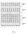
- FIG. 1 is a plan view showing a part of the semiconductor device according to the first embodiment of the present invention.
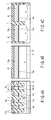
- FIGS. 2A to 2C are cross-sectional views schematically showing a main part of the semiconductor device according to the first embodiment of the present invention.
- FIGS. 2A and 2B are cross-sectional views taken along lines IIA-IIA and IIB-IIB, respectively.
- FIG. 2C is a cross-sectional view of a transistor (peripheral transistor) in a peripheral circuit region.
- the semiconductor device has selection gate (selection gate transistor) regions and memory cell (memory cell transistor) regions.
- the memory cell region is interposed between selection gate regions.
- An element isolation insulating film 1 of a shallow trench isolation (STI) structure is formed on a semiconductor substrate (not shown) constituted of, for example, silicon.
- the element isolation insulating film 1 is a region formed by a plurality of bands arranged in the vertical direction in the drawing so as to divide an element region (active region) 2 of a semiconductor substrate 11.
- a plurality of control gate electrodes 3 extend in the lateral direction of the drawing. Further, the control gate electrodes 3 are arranged at intervals in the vertical direction of the drawing.
- the control gate electrodes 3 in the memory cell region each constitute a part of a memory cell transistor, and the control gate electrodes 3 in the selection gate region each constitute a part of a selection gate transistor.
- Floating gate electrodes are provided below the control gate electrodes 3 and on the surface of the semiconductor substrate in the element region.
- the floating gate electrodes are arranged at intervals in the lateral direction of the drawing.
- an n type well 12 and a p type well 13 are formed on the surface of the semiconductor substrate formed of, for example, silicon or the like. Further, the element isolation insulating film 1 is formed on the surface of the semiconductor substrate 11. The element isolation insulating film 1 protrudes from the surface of the semiconductor substrate 11.
- Insulating films 14A and 14B constituted of, for example, a silicon dioxide film are provided on the surface of the semiconductor substrate 11 of the element region 2.
- the insulating film 14A constitutes a part of the memory cell transistor, and functions as a tunnel insulating film.
- the insulating film 14B constitutes a part of each of the selection gate transistor and the peripheral transistor, and functions as a gate insulating film. Stacked gate electrode structures adjacent to each other so as to be separate from each other are provided on the insulating films 14A and 14B.
- Each stacked gate electrode structure has a pattern as shown in FIG. 1 on the plan. As shown in FIGS. 2A, 2B, and 2C, each stacked gate electrode structure includes a floating gate electrode 15, an inter-electrode insulating film 16, a control gate electrode 3, and the like.
- a floating gate electrode 15 is provided on each of the insulating films 14A and 14B.
- the floating gate electrode 15 is constituted of, for example, conductive polysilicon.
- the floating gate electrode 15 has a thickness of, for example, 85 nm according to the 55 nm rule.
- the inter-electrode insulating film 16 is provided on the floating gate electrode 15.
- the inter-electrode insulating film 16 is constituted of, for example, a stacked film (ONO film) of a silicon dioxide film, a silicon nitride film, and a silicon dioxide film, or a stacked film (NONON film) of a silicon nitride film, a silicon dioxide film, a silicon nitride film, a silicon dioxide film, and a silicon nitride film, or a dielectric film containing aluminum or hafnium.
- the selection gate transistor and the peripheral transistor have a structure in which the inter-electrode insulating film 16 has an opening 21 penetrating the top surface and the undersurface, and the control gate electrode 3 that is the upper layer and the floating gate electrode 15 that is the lower layer are electrically connected to each other.
- the control gate electrode 3 is provided on the inter-electrode insulating film 16.
- the control gate electrode 3 has stacked two conductive layers 3a and 3b.
- the first part 3a of the first control gate is constituted of, for example, electrically conductive polysilicon, and has a thickness of, for example, 40 nm according to the 55 nm rule.
- the first part 3a of the control gate electrode 3 of the selection transistor and the peripheral transistor has an opening 21 penetrating the top surface and the undersurface.
- the opening 21 of the first part 3a of the control gate electrode 3 and the opening 21 of the inter-electrode insulating film 16 coincide with each other in the position on the plan.
- the second part 3b of the control gate electrode 3 has a thickness of, for example, 100 nm according to the 55 nm rule.
- a part of the second part 3b of the control gate electrode 3 fills up the opening 21, and is connected to the floating gate electrode 15.
- the second part 3b of the control gate electrode 3 is constituted of, for example, conductive polysilicon, and is partly or wholly tuned into the metallic silicide by the transistor. More specifically, in the selection gate transistor and the peripheral transistor, the top surface and the side surface are turned into the metallic silicide, and a metallic silicide film 22 is formed in these regions. In the selection gate transistor and the peripheral transistor, the metallic silicide film 22 has a thickness at the top surface and a width on the side surface of, for example, 15 to 40 nm.
- the second part 3b of the control gate electrode 3 is wholly turned into the metallic silicide, and a metallic silicide film 22 constitutes the second part 3b of the selection gate electrode.
- the second part 3b of the control gate electrode 3 of the memory cell transistor is wholly turned into the metallic silicide, and only the top surface and the side surface of the second part 3b of the control gate electrode 3 of the selection gate transistor and the peripheral transistor are turned into the metallic silicide.
- each metallic silicide film 22 is formed to have such a feature, and hence each metallic silicide film 22 has the following relationship.
- the thickness Db of a part of the metallic silicide film 22 closer to the center than the region turned into the metallic silicide, of the side surface of the second part 3b of the control gate electrode of the selection gate transistor is smaller than the thickness Dc of the metallic silicide film 23 of the side surface of the second part 3b.
- the thickness Dd of a part of the metallic silicide film 22 closer to the center than the region turned into the metallic silicide, of the side surface of the second part 3b of the control gate electrode of the peripheral transistor is smaller than the thickness De of the metallic silicide film 23 of the side surface of the second part 3b.
- the thickness of the metallic silicide film 22, in a vertical direction (a direction which is parallel to the main surface of the semiconductor substrate 11), on a side surface of the second part 3b is equal to a thickness Db, Dd.
- the thickness Db, Dd is smaller than the thickness Da of the metallic silicide film 22 of the second part 3b of the control gate electrode 3 of the cell transistor.
- the second part 3b of the cell transistor is typically turned into the silicide as a whole, and the thickness Da is therefore the same at any part of the second part 3b of the cell transistor.
- the present invention is not limited to this. That is, at least a region of the second part 3b above a predetermined position should only be turned into the silicide as a whole. Specifically, for example, the upper half part of the second part 3b is wholly turned into the silicide.
- the thickness of the second part 3b is determined by a resistance value required of the second part 3b. That is, the smaller the required resistance value is, the thicker the silicide film 22 on the top surface of the second part 3b becomes.
- the thickness of the second part 3b of the memory cell transistor is, at the maximum, the entirety of the control gate electrode 3, i.e., the entirety of the first part 3a and the second part 3b.
- the region above the undersurface of the second part 3b is turned into the silicide.
- the method of controlling the thickness of the silicide film 22 will be described later in the description of the manufacturing method.
- Source/drain diffusion regions 23 of a conduction type corresponding to the conduction type of each transistor are formed so as to sandwich the channel region under each stacked gate electrode structure of the cell transistor, selection transistor, and peripheral transistor.
- the source/drain diffusion region 23 has, at a part on the opposite side of the memory cell transistor of the selection gate transistor, and at the peripheral transistor, a part 23a for reducing the resistance between itself and the contact plug, in contact with the channel region, and a part 23b having a higher concentration than the part 23a.
- the sidewall insulating film 24 is formed so as to allow it to reach an intermediate height of the stacked gate electrode structure, and the height thereof will be described later in detail.
- the sidewall insulating film 24 is not provided at the end on the opposite side of the memory cell transistor of the selection gate transistor. This is because to make the distance between respective selection gate transistors large. However, this configuration is not indispensable, and the sidewall insulating film 24 may be provided.
- a barrier film 25 constituted of, for example, a silicon dioxide film or a silicon nitride film or the like is provided.
- the barrier film 25 has a function of an etching stopper.
- the barrier film 25 is also provided on the source/drain diffusion region 23, and the element isolation insulating film 1.
- the region up to the same height as the sidewall insulating film 24 between the respective transistors is filled up with an inter-layer insulating film 31.
- the inter-layer insulating film 31 is constituted of, for example, a silicon oxide film.
- a covering insulating film 32 is provided on the side surface which is not covered with the sidewall insulating film 24 of the stacked gate electrode structure, and on the top surface of the control gate electrode 3.
- the covering insulating film 32 also covers the top surface of the inter-layer insulating film 31.
- the covering insulating film 32 is constituted of, for example, a silicon dioxide film or a silicon nitride film, and has a thickness of, for example, 30 nm.
- An inter-layer insulating film 33 constituted of, for example, a silicon dioxide film is provided on the entire surface of the covering insulating film 32.
- a wiring layer 34 is provided in the inter-layer insulating film 33.
- a plug 35 extending from the wiring layer 34, penetrating the covering insulating film 32, and reaching the metallic silicide film 22 is provided at the lower part of the wiring layer 34. Further, a plug 35 penetrating the covering insulating film 32, inter-layer insulating film 31, and barrier film 25, and reaching the source/drain diffusion region 23 is provided in a predetermined position at the lower part of the wiring layer 34.
- FIGS. 2A, 2B, and 2C Next, a method of manufacturing a semiconductor device shown in each of FIGS. 2A, 2B, and 2C will be described below with reference to FIGS. 3A, 3B, and 3C to 14A, 14B, and 14C.
- FIGS. 3A to 14A show a manufacturing method of the structure shown in FIG. 2A in the order of sequence.
- FIGS. 3B to 14B show a manufacturing method of the structure shown in FIG. 2B in the order of sequence.
- FIGS. 3C to 14C show a manufacturing method of the structure shown in FIG. 2C in the order of sequence.
- wells 12 and 13 are formed by using a lithography step and ion implantation.
- an insulating film 14a which will become the insulating film 14A or 14B is formed on the entire surface of the semiconductor substrate 11 by, for example, thermal oxidation.
- a conductive film 15a which will become the floating gate electrode 15 is formed on the insulating film 14a by, for example, chemical vapor deposition (CVD).
- a mask material 41 constituted of, for example, SiN is formed on the conductive film 15a by, for example, CVD.
- trenches are formed in a region in which the element isolation insulating film 1 is scheduled to be formed by using a lithography step and the etching technique.
- the trenches penetrate the mask material 41, conductive film 15a, insulating film 14a, and reach the surface of the semiconductor substrate 11.
- the trenches are filled up with a film serving as a material for the element isolation insulating film 1.
- the unnecessary film on the mask material 41 is removed by, for example, chemical mechanical polishing (CMP), thereby forming the element isolation insulating film 1.
- CMP chemical mechanical polishing
- the mask material 41 is removed by, for example, wet etching.
- the top surface of the element isolation insulating film 1 is etched back to a position lower than, for example, the top surface of the electrode film 15a by, for example, reactive ion etching (RIE), wet etching, and the like.
- RIE reactive ion etching
- an insulating film 16a which will become the inter-electrode insulating film 16 is formed on the entire surface of the structure obtained by the steps performed up to now. As a result of this, in the cell transistor region, the exposed side surfaces and top surfaces of the conductive film 15a are covered with the insulating film 16a.
- a conductive film 3aa which will become the first part 3a of the control gate electrode is formed on the entire surface of the insulating film 16a by, for example, the CVD method.
- the conductive film 3aa is constituted of, for example, conductive polysilicon, fills up the regions above the element isolation insulating films 1 formed between the conductive films 15a, and is arranged on the insulating film 16a formed on the top surfaces of the conductive films 15a.
- an opening 21 or openings 21 reaching the conductive film 15a is or are formed in at least part of the conductive film 3aa and insulating film 16a in the region in which the selection gate transistor or the peripheral transistor is scheduled to be formed, by the lithography step and etching technique.
- a material film 3ba which will become the second part 3b of the control gate electrode 3 is formed on the entire surface of the structure obtained by the steps performed up to now by, for example, CVD.
- the material film 3ba is constituted of, for example, conductive polysilicon.
- a part of the material film 3ba fills the opening 21, and is connected to the conductive film 15a.
- a mask material 42 is formed on the entire surface of the material film 3ba by, for example, CVD.
- patterning is performed by the lithography step and etching technique in such a manner that the mask material 42 remains in regions in which the stacked gate electrode structure of the cell transistor, selection gate transistor, and peripheral transistor are scheduled to be formed.
- the material film 3ba, conductive film 3aa, insulating film 16a, conductive film 15a, and insulating film 14a are etched by using the mask material 42.
- a stacked gate electrode structure of each transistor constituted of the second part 3b of the control gate electrode 3, first part 3a, inter-electrode insulating film 16, and floating gate electrode 15, is formed.
- the tunnel insulating film 14A and the gate insulating film 14B are formed.
- the source/drain diffusion region 23 is formed, and in each of the selection gate transistor and peripheral transistor, the low concentration part 23a of the source/drain diffusion region 23 is formed, by ion implantation using the stacked gate electrode structure as a mask. Further, in this ion implantation step, ions are implanted in the second part 3b of the control gate electrode, thereby turning the second part 3b into a conductive film. A damage of the ion-implantation which is targeted to the semiconductor substrate is reduced by leaving the insulating film 14a in an etching of a manufacturing process of the stacked gate electrode structure.
- the p type source/drain diffusion region and the region in which the control gate electrode is to be formed are covered with a mask material (not shown).
- the n type source/drain diffusion region and the region in which the control gate electrode is to be formed are covered with a mask (not shown).
- the order of implanting n type and p type impurities can be arbitrarily selected.
- an insulating film which will become the sidewall insulating film 24 is formed on the entire surface of the structure obtained by the steps performed up to now by, for example, CVD.
- the side wall insulating film 24 is also formed on the insulating film 14A, when the insulating film 14A is leaved in the etching process.
- the thickness of this insulating film is, for example, 20 to 60 nm. Then, of parts of the insulating film, a part on the mask material 42 and a part on the surface of the semiconductor substrate 11 are removed by the etching technique, thereby forming the sidewall insulating film 24.
- the sidewall insulating film 24 is constituted of a material which can obtain an etching selectivity ratio with respect to the floating gate electrode 15, first part 3a and second part 3b of the control gate electrode 3, i.e., for example, a silicon dioxide film or silicon nitride film, as described above.
- the high concentration part 23b of the source/drain diffusion region 23 is formed by ion implantation using the mask material 42 and the sidewall insulating film 24 as a mask.
- regions not to be subjected to implantation are covered with a mask material (not shown) in accordance with the conduction type of impurities to be implanted.
- a mask material (not shown) having an opening above the sidewall insulating film 24 disposed on the opposite side of the memory cell transistor of the selection gate transistor is formed by the lithography step. Then, the sidewall insulating film 24 on the opposite side of the memory cell transistor of the selection gate transistor is removed by the etching using this mask material. Then, the mask material is removed.
- a barrier film 25 is formed on the entire surface of the structure obtained by the steps performed up to now by, for example, CVD.
- a part on the sidewall on the opposite side of the memory cell transistor of the stacked gate electrode structure of the selection gate transistor, a part on the mask material 42, the surface of the semiconductor substrate 11, a part on the sidewall insulating film 24 of the peripheral transistor, and the element isolation insulating film 1 of the peripheral transistor region are covered with the barrier film 25.
- an inter-layer insulating film 31 is formed on the entire surface of the structure obtained by the steps performed up to now by, for example, CVD.
- the top surface of the inter-layer insulating film 31 is caused to retreat until the mask material 42 becomes exposed and, at the same time, the mask material 42 on the top surface of the second part 3b of the control gate electrode 3 is removed by, for example, CMP.
- the top surface of the sidewall insulating film 24 is caused to retreat to at least a position slightly above the boundary between the first part 3a and the second part 3b of the control gate electrode 3 by using the etching technique. As a result of this, the entire top surface and almost the entire side surface of the second part 3b of the control gate electrode 3 of the cell transistor are exposed.
- the top surface of the barrier film 25 and the top surface of the inter-layer insulating film 31 also retreat.
- the retreated top surfaces of the barrier film 25 and the inter-layer insulating film 31 are positioned at the same level as the retreated top surface of the sidewall insulating film 24 when the sidewall insulating film 24, barrier film 25, and the inter-layer insulating film 31 are made of the same material, and the etching selectivity ratio is substantially zero.
- the entire top surface and almost the entire side surface of the second part 3b of the control gate electrode 3 of the selection gate transistor are exposed.
- the peripheral transistor too, the entire top surface and about half the side surface of the second part 3b of the control gate electrode are exposed.
- a metallic film 43 for silicidization is formed on the entire surface of the structure obtained by the steps performed up to now by, for example, CVD or sputtering.
- the metallic film 43 covers the top surface and exposed side surface of the second part 3b of the control gate electrode 3 of each transistor.
- the material of the metallic film 43 is, for example, cobalt, titanium, nickel, and the like in accordance with the material of the metallic silicide film 22.
- the thickness of the metallic film 43 is determined in such a manner that, of the part of the second part 3b of the control gate electrode 3 of the cell transistor, the entire part corresponding to the same thickness as the thickness of the exposed side surface is silicidized, which will be explained below.
- metallic atoms in the metallic film 43 diffuse into the second part 3b of the control gate electrode 3, and turns to the metallic silicide film 23.
- metallic atoms advance also from the side surface of the second part 3b of the control gate electrode, and hence a wide range of the second part 3b of the control gate electrode 3 can be silicidized without requiring the metallic atoms to diffuse over a long distance unlike in the case where the metallic atoms advance only from the top surface.
- the thickness of the metallic film 43 is determined in such a manner that a distal end of a silicide reaction advancing from the side surface of the second part 3b reaches a distal end of a silicide reaction advancing from the other side surface opposite to the above side surface, whereby of the part of the second part 3b of the control gate electrode 3 of the cell transistor, the entire part corresponding to the same thickness as the thickness of the exposed side surface becomes the metallic silicide film 25.
- the diffusion of the metallic atoms changes also depending on the time of the heat step.
- the heat step may possibly affect adversely the other part which is already formed at the time of the heat step.
- the thickness of the metallic film 43 is determined in such a manner that the metallic silicide film 22 of the above-mentioned range can be formed even by a heat step of such a degree that the other part is not adversely affected.
- the thickness of the metallic film 43 can be set, for example, in a range of 20 to 60% of the width of the second part 3b of the control gate electrode 3, or in a range of 12 to 20 nm according to the 55 nm rule.
- the metallic silicide film 22 is formed by reacting the metallic film with the second part 3b of the control gate electrode 3 by a heat treatment.
- the metallic film 43 has the thickness described above, and the metallic atoms diffuse from the top surface and side surfaces of the second part 3b of the control gate electrode 3. Accordingly, by appropriately adjusting the heat treatment time, the distal end of the silicidization advancing from the side surface of the second part 3b reaches the distal end of the silicidization advancing from the side surface on the opposite side of this side surface. As a result of this, of the part of the second part 3b of the control gate electrode 3 of the cell transistor, the part having substantially the same thickness as the second part 3b is wholly turned into the metallic silicide.
- the widths of the selection gate transistor and the peripheral transistor in the channel length direction are larger than that of the cell transistor. Accordingly, the silicidization advancing from the side surface of the second part 3b of the control gate electrode 3 of each of the selection gate transistor and the peripheral transistor does not reach the silicidized region extending from the side surface on the opposite side of the above side surface.
- the part to be silicidized is only the surface of the second part 3b including the top surface and side surface of the control gate electrode 3, and the part further inside the above part is not silicidized.
- the thickness Db is smaller than the thickness Dc
- the thickness Dd is smaller than the thickness De
- the thickness Db and thickness Dd are smaller than the thickness Da.
- the thickness of the metallic silicide film 22, in a vertical direction (a direction which is parallel to the main surface of the semiconductor substrate 11), on a side surface of the second part 3b is equal to a thickness Db, Dd.
- the part that does not contribute to metal-silicidization i.e., the part which is not in contact with the second part 3b of the control gate electrode 3 is removed by using the etching technique.
- the covering insulating film 32 is formed on the entire surface of the structure obtained by the steps performed up to now by, for example, CVD.
- the covering insulating film 32 covers the metallic silicide film 22 and also covers the top surface of the inter-layer insulating film 31.
- the inter-layer insulating film 33 is formed on the entire surface of the covering insulating film 32 by, for example, CVD. Then, a wiring trench and contact hole are formed by using the lithography step and etching technique, and a conductive film is formed in the wiring trench and contact hole by CVD and sputtering. As a result of this, the wiring layer 34 and the plug 35 are formed.
- an oxide film 51 is provided under the covering insulating film 32. That is, the oxide film 51 covers the entire surface of the metallic silicide film 22, and also covers the top surfaces of the sidewall insulating film 24, barrier film 25, and inter-layer insulating film 31. Further, the covering insulating film 32 is provided on the entire surface of the oxide film 51.
- the oxide film 51 is constituted of a silicon dioxide film, and has a thickness of 50 nm.
- a void is generated in the upper surface of the side wall insulating film 24 formed between the memory cell transistors.
- the void also extends to the middle portion of the side wall insulating film 24.
- the void is filled by the covering insulating film (for instance, SiN film) 32, when the covering insulating film 32 is formed on the side wall insulating film 24.
- the memory cell transistors which is located the both sides of the void have a large parasitic capacitance, as the result, the write error and the read error (so-called an inter-cells interference) generated.
- the upper portion of the void is closed, when the side wall insulating film 24 is covered by the oxide film 51. As the result, the void is not filled by the covering insulating film 32.
- the inter-cells interference becomes small.
- the dielectric constant of the oxide film 51 is lower than that of the covering insulating film 32.
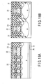
- the method of manufacturing the structure shown in FIGS. 19A, 19B, and 19C is as shown below.
- the void is formed between the memory cell transistors in the process of forming the side wall insulating film 24, because a space between the memory cell transistors is narrow.
- the upper surface of the side wall insulating film 24 is lower than that of the void in a process that the upper surface of the side wall insulating film 24 is backed at the upper portion of the boundary area between the first part 3a and the second part 3b of the control gate electrode 3.
- the void which has an opening on the upper surface of the side wall insulating film 24 and extends to the middle portion of the side wall insulating film 24 is formed.
- the oxide film 51 is formed by, for instance, CVD or a spattering method, on the structure which is obtained by the process in FIGS. 13A, 13B, and 13C.
- the oxide film 51 is formed by a depositing condition that the oxide film 51 covers the opening of the void and does not fill the void. If the oxide film 51 is filled in the void, the inter-cells interference is small because the dielectric constant of the oxide film 51 is lower than that of the covering insulating film 32.
- the covering insulating film 32 is formed on the entire surface of the oxide film 51 in the same manner as that in the step shown in FIGS. 14A, 14B, and 14C.
- the covering insulating film 32 does not filled in the void because the oxide film 51 covers the opening of the void.
- the step subsequent to the present step is the same as that has been described previously with reference to FIGS. 2A, 2B, and 2C.
- a metallic film for forming the metallic silicide film 22 is formed on the sidewall of the control gate electrode 3. Accordingly, metallic atoms for silicidization diffuse not only from the top surface of the control gate electrode 3 but also from the side surfaces thereof. Hence, it is possible to form a thick metallic silicide film 22 over the entire surface of the control gate electrode 3 in the planar direction without depending only on the diffusion of metallic atoms from the top surface.
- the distance by which the metallic atoms have to diffuse and which is required to turn the desired thickness into the metallic silicide film 22 is shorter than that in the case where the silicidization advances only from the top surface of the control gate electrode 3. Accordingly, the thickness of the metallic silicide film 22 is prevented from varying from cell transistor to cell transistor, and progress in deterioration by agglomeration can be suppressed.
- a second embodiment differs from the first embodiment in the step of exposing a second part 3b of a control gate electrode.
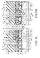
- FIG. 15A is a cross-sectional view taken along line IIB-IIB in FIG. 1, and is a cross-sectional view in the same position as FIG. 2B of the first embodiment.
- FIG. 15B is a cross-sectional view of a peripheral transistor, and is a cross-sectional view in the same position as FIG. 2C of the first embodiment.
- the cross-sectional view taken along line IIA-IIA in FIG. 1 is the same as that of the first embodiment (FIG. 2A).
- the entire side surface on the opposite side of the cell transistor of the stacked gate electrode structure of the selection gate transistor is covered with a barrier film 25.
- the entire side surface of the stacked gate electrode structure of the peripheral transistor is covered with a sidewall insulating film 24.
- the entire side surface of the sidewall insulating film 24 is covered with the barrier film 25.
- the space is filled with an inter-layer insulating film 31 up to the same height as the top surface of a control gate electrode 3, and the top surfaces of the inter-layer insulating film 31 and the barrier film 25 are covered with a covering insulating film 32.
- the other structures are the same as the first embodiment.
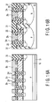
- FIGS. 15A and 15B Next, a method of manufacturing the semiconductor device shown in FIGS. 15A and 15B will be described below with reference to FIGS. 16A, 16B to 18A, and 183.
- FIGS. 16A to 18A show a manufacturing method of the structure shown in FIG. 15A in the order of sequence.
- FIGS. 16B to 18B show a manufacturing method of the structure shown in FIG. 15B in the order of sequence.
- the same steps as those shown in FIGS. 3A, 3B, 3C to 10A, 10B, and 10C of the first embodiment are performed.
- the top surface of the inter-layer insulating film 31 is caused to retreat until a mask material 42 is exposed as in the step shown in FIGS. 11B and 11C.
- the mask material 42 on the top surface of a second part 3b of the control gate electrode 3 is removed.
- a mask material (not shown) having an opening above the cell transistor is formed on the control gate electrode 3. Then, a mask material (not shown) having an opening above the cell transistor is formed on the control gate electrode 3. Then, the top surface of the sidewall insulating film 24 of the cell transistor is caused to retreat in accordance with the condition described in the first embodiment by etching using the mask material as a mask. At this time, the top surface of the sidewall insulating film 24 of the selection gate transistor may be or may not be caused to retreat likewise. Then, the mask material is removed.
- a metallic film 43 is formed on the entire surface of the structure obtained by the steps performed up to now as in the step shown in FIGS. 12B and 12C.
- the metallic film 43 is formed only, of parts of the second part of the control gate electrode 3 of each transistor, on the side surface of the cell transistor and the side surface on the cell transistor side of the selection gate transistor.
- the metallic film 43 is formed only on the top surface of the control gate electrode 3.
- a part of the second part 3b of the control gate electrode 3 in contact with the metallic film 43 is silicidized.
- a region defined by the same thickness as the thickness extending over the entirety in the planar direction and exposed is silicidized.
- the second part 3b of the control gate electrode 3 of the selection gate transistor only a part near the surface of the side surface on the cell transistor side and the top surface are silicidized.
- the peripheral transistor only a part near the surface of the top surface of the second part 3 of the control gate electrode 3 is silicidized.
- FIGS. 18A and 18B a covering insulating film 32 is formed on the entire surface of the structure obtained by the steps performed up to now as in the step shown in FIGS. 14B and 14C. Then, as shown in FIGS. 15A and 15B, an inter-layer insulating film 33, wiring layer 34, plug 35, and the like are formed.
- a metallic film for forming a metallic silicide film 22 is formed on the sidewall of the control gate electrode 3. Accordingly, the same effect as that of the first embodiment can be obtained.
- the present invention is not limited to the first and second embodiments described above in the idea and the category of the present invention, and their alteration examples and modification examples are also included in the scope of the present invention.
Landscapes
- Engineering & Computer Science (AREA)
- Manufacturing & Machinery (AREA)
- Physics & Mathematics (AREA)
- Condensed Matter Physics & Semiconductors (AREA)
- General Physics & Mathematics (AREA)
- Computer Hardware Design (AREA)
- Microelectronics & Electronic Packaging (AREA)
- Power Engineering (AREA)
- Chemical Kinetics & Catalysis (AREA)
- Chemical & Material Sciences (AREA)
- Semiconductor Memories (AREA)
- Non-Volatile Memory (AREA)
- Internal Circuitry In Semiconductor Integrated Circuit Devices (AREA)
Abstract

Description
- The present invention relates to a semiconductor device and a method of manufacturing the same and, more particularly, to, for example, a stacked transistor having a structure in which a floating gate electrode and a control gate electrode are provided through an inter-electrode insulating film and a method of manufacturing the same.
- A nonvolatile semiconductor storage device using a transistor having a structure in which a floating gate electrode, an inter-electrode insulating film, and a control gate electrode are stacked is known. By using such a transistor as a memory cell and connecting a plurality of such memory cells in series, a NAND cell string of a so-called NAND flash memory is constituted.
- An attempt is made to reduce the resistance value of the control gate electrode by using a metallic silicide film in a part of an electrode film serving as a control gate electrode of the NAND flash memory. Turning an electrode film into a metallic silicide film is performed by depositing a metallic film for constituting a metallic silicide film on a top surface of an electrode film constituted of polysilicon, and heating the polysilicon film and the metallic film. As a result of this, metallic atoms diffuse into the polysilicon film, and react with the polysilicon, thereby forming a metallic silicide film.
- Recently, as a result of turning a control gate electrode film into a metallic silicide film, following phenomena have been confirmed. That is, the phenomena are an increase in the resistance value of a control gate electrode, an increase in the variation in the resistance value of a control gate electrode in a memory cell area, progress in deterioration of a control gate electrode caused by an increase in agglomeration, and the like. Incidentally, agglomeration implies a phenomenon in which metallic atoms move because of formation of crystal grains.
- These phenomena are assumed to be due to progress in micronization of a semiconductor device. The phenomena will be described below. With the pursuit of micronization of the semiconductor storage device, sizes of parts in the semiconductor storage device continue becoming smaller. With the micronization, a width of a control gate electrode becomes narrower, thereby increasing an aspect ratio (ratio of a height to a width) of the control gate electrode.
- An increase in the aspect ratio of the control gate electrode makes it necessary to form a metallic silicide film having a high aspect ratio. As described above, when a metallic silicide film is formed, metallic atoms diffuse into the polysilicon film from a metallic element film provided on the polysilicon film. That is, the metallic atoms diffuse in the film thickness direction of the polysilicon film. Accordingly, the volume of the polysilicon to be turned into the metallic silicide is determined in accordance with the degree of diffusion of the metallic atoms. In order to equalize characteristics among memory cells, it is desirable that the volume of the polysilicon to be turned into the metallic silicide be uniform among the control gate electrodes. That is, it is necessary to appropriately control diffusion of the metallic atoms in the film thickness direction of the control gate electrode. However, in general, the deeper the region of the polysilicon film desired to be turned into the metallic silicide becomes in the depth direction of the polysilicon film, the more difficult control of the diffusion length of the metallic atoms becomes. For this reason, an increase in the aspect ratio of the control gate electrode described above causes the diffusion length of the metallic atoms to largely vary among the control gate electrodes. As a result, an increase in the resistance value of a control gate electrode, an increase in the variation in the resistance value of a control gate electrode among cells, progress in deterioration of a control gate electrode caused by an increase in agglomeration, and the like described above occur.
- An example is disclosed in
USP 7,012,295 andUSP 7,122,430 (Both are based on Jpn. Pat. Appln. KOKAI PublicationNo. 2005-26589 ) in which a control gate of a memory cell and a selection transistor and a diffusion layer of the selection transistor are turned into the silicide. - A semiconductor device of an aspect of the present invention comprising a first insulating film provided on a semiconductor substrate in a cell transistor region, a first conductive film provided on the first insulating film, an inter-electrode insulating film provided on the first conductive film, a second conductive film provided on the inter-electrode insulating film and having a first metallic silicide film on a top surface thereof, first source/drain regions formed on a surface of the semiconductor substrate and sandwiching a region under the first insulating film, a second insulating film provided on the semiconductor substrate in at least one of a selection gate transistor region and a peripheral transistor region, a third conductive film provided on the second insulating film and having a second metallic silicide film having a thickness smaller than a thickness of the first metallic silicide film on a top surface thereof, and a second source/drain regions formed on the surface of the semiconductor substrate and sandwiching a region under the second insulating film.
- The invention can be more fully understood from the following detailed description when taken in conjunction with the accompanying drawings, in which:
- FIG. 1 is a plan view of a semiconductor storage device according to a first embodiment.
- FIGS. 2A to 2C show cross-sectional views of a semiconductor storage device according to the first embodiment.
- FIGS. 3A to 3C show cross-sectional views each showing a part of manufacturing steps of the semiconductor device shown in FIGS. 2A to 2C.
- FIGS. 4A to 4C show cross-sectional views showing steps subsequent to those shown in FIGS. 3A to 3C.
- FIGS. 5A to 5C show cross-sectional views showing steps subsequent to those shown in FIGS. 4A to 4C.
- FIGS. 6A to 6C show cross-sectional views showing steps subsequent to those shown in FIGS. 5A to 5C.
- FIGS. 7A to 7C show cross-sectional views showing steps subsequent to those shown in FIGS. 6A to 6C.
- FIGS. 8A to 8C show cross-sectional views showing steps subsequent to those shown in FIGS. 7A to 7C.
- FIGS. 9A to 9C show cross-sectional views showing steps subsequent to those shown in FIGS. 8A to 8C.
- FIGS. 10A to 10C show cross-sectional views showing steps subsequent to those shown in FIGS. 9A to 9C.
- FIGS. 11A to 11C show cross-sectional views showing steps subsequent to those shown in FIGS. 10A to 10C.
- FIGS. 12A to 12C show cross-sectional views showing steps subsequent to those shown in FIGS. 11A to 11C.
- FIGS. 13A to 13C show cross-sectional views showing steps subsequent to those shown in FIGS. 12A to 12C.
- FIGS. 14A to 14C show cross-sectional views showing steps subsequent to those shown in FIGS. 13A to 13C.
- FIGS. 15A and 15B show cross-sectional views of a semiconductor storage device according to a second embodiment.
- FIGS. 16A and 16B show cross-sectional views showing a art of manufacturing steps of the semiconductor device shown in FIGS. 15A and 15B.
- FIGS. 17A and 17B show cross-sectional views showing steps subsequent to those shown in FIGS. 16A and 16B.
- FIGS. 18A and 18B show cross-sectional views showing steps subsequent to those shown in FIGS. 17A and 17B.
- FIGS. 19A to 19C show plan views of a semiconductor storage device according to a modification example of the first embodiment.
- FIGS. 20A to 20C show cross-sectional views showing a part of manufacturing steps of the semiconductor device shown in FIGS. 19A to 19C.
- Embodiments of the present invention will be described below with reference to the accompanying drawings. Incidentally, constituent elements having substantially the same functions and configurations are denoted by the same reference symbols and a duplicated description will be given only when necessary.
- In this embodiment, description will be given by taking a NAND flash memory as an example. However, the present invention is not limited to this. Needless to say, the present invention can be applied to a NOR flash memory.
- A semiconductor device according to a first embodiment of the present invention will be described below with reference to FIGS. 1, 2A, 2B, 2C to 14A, 14B, and 14C. FIG. 1 is a plan view showing a part of the semiconductor device according to the first embodiment of the present invention. FIGS. 2A to 2C are cross-sectional views schematically showing a main part of the semiconductor device according to the first embodiment of the present invention. FIGS. 2A and 2B are cross-sectional views taken along lines IIA-IIA and IIB-IIB, respectively. FIG. 2C is a cross-sectional view of a transistor (peripheral transistor) in a peripheral circuit region.
- As shown in FIG. 1, the semiconductor device has selection gate (selection gate transistor) regions and memory cell (memory cell transistor) regions. The memory cell region is interposed between selection gate regions. An element
isolation insulating film 1 of a shallow trench isolation (STI) structure is formed on a semiconductor substrate (not shown) constituted of, for example, silicon. The elementisolation insulating film 1 is a region formed by a plurality of bands arranged in the vertical direction in the drawing so as to divide an element region (active region) 2 of asemiconductor substrate 11. - A plurality of
control gate electrodes 3 extend in the lateral direction of the drawing. Further, thecontrol gate electrodes 3 are arranged at intervals in the vertical direction of the drawing. Thecontrol gate electrodes 3 in the memory cell region each constitute a part of a memory cell transistor, and thecontrol gate electrodes 3 in the selection gate region each constitute a part of a selection gate transistor. - Floating gate electrodes are provided below the
control gate electrodes 3 and on the surface of the semiconductor substrate in the element region. The floating gate electrodes are arranged at intervals in the lateral direction of the drawing. - As shown in FIGS. 2A to 2C, an n type well 12 and a p type well 13 are formed on the surface of the semiconductor substrate formed of, for example, silicon or the like. Further, the element
isolation insulating film 1 is formed on the surface of thesemiconductor substrate 11. The elementisolation insulating film 1 protrudes from the surface of thesemiconductor substrate 11. - Insulating
films semiconductor substrate 11 of theelement region 2. The insulatingfilm 14A constitutes a part of the memory cell transistor, and functions as a tunnel insulating film. The insulatingfilm 14B constitutes a part of each of the selection gate transistor and the peripheral transistor, and functions as a gate insulating film. Stacked gate electrode structures adjacent to each other so as to be separate from each other are provided on the insulatingfilms - Each stacked gate electrode structure has a pattern as shown in FIG. 1 on the plan. As shown in FIGS. 2A, 2B, and 2C, each stacked gate electrode structure includes a floating
gate electrode 15, an inter-electrodeinsulating film 16, acontrol gate electrode 3, and the like. - In the stacked gate electrode structure, a floating
gate electrode 15 is provided on each of the insulatingfilms gate electrode 15 is constituted of, for example, conductive polysilicon. The floatinggate electrode 15 has a thickness of, for example, 85 nm according to the 55 nm rule. - The inter-electrode
insulating film 16 is provided on the floatinggate electrode 15. The inter-electrodeinsulating film 16 is constituted of, for example, a stacked film (ONO film) of a silicon dioxide film, a silicon nitride film, and a silicon dioxide film, or a stacked film (NONON film) of a silicon nitride film, a silicon dioxide film, a silicon nitride film, a silicon dioxide film, and a silicon nitride film, or a dielectric film containing aluminum or hafnium. - The selection gate transistor and the peripheral transistor have a structure in which the inter-electrode insulating
film 16 has anopening 21 penetrating the top surface and the undersurface, and thecontrol gate electrode 3 that is the upper layer and the floatinggate electrode 15 that is the lower layer are electrically connected to each other. - The
control gate electrode 3 is provided on the inter-electrode insulatingfilm 16. Thecontrol gate electrode 3 has stacked twoconductive layers first part 3a of the first control gate is constituted of, for example, electrically conductive polysilicon, and has a thickness of, for example, 40 nm according to the 55 nm rule. Thefirst part 3a of thecontrol gate electrode 3 of the selection transistor and the peripheral transistor has anopening 21 penetrating the top surface and the undersurface. Theopening 21 of thefirst part 3a of thecontrol gate electrode 3 and theopening 21 of the inter-electrode insulatingfilm 16 coincide with each other in the position on the plan. - The
second part 3b of thecontrol gate electrode 3 has a thickness of, for example, 100 nm according to the 55 nm rule. A part of thesecond part 3b of thecontrol gate electrode 3 fills up theopening 21, and is connected to the floatinggate electrode 15. By virtue of this structure, in the selection gate transistor and the peripheral transistor, the floatinggate electrode 15 and thecontrol gate electrode 3 integrally constitute a gate electrode of the transistor. - The
second part 3b of thecontrol gate electrode 3 is constituted of, for example, conductive polysilicon, and is partly or wholly tuned into the metallic silicide by the transistor. More specifically, in the selection gate transistor and the peripheral transistor, the top surface and the side surface are turned into the metallic silicide, and ametallic silicide film 22 is formed in these regions. In the selection gate transistor and the peripheral transistor, themetallic silicide film 22 has a thickness at the top surface and a width on the side surface of, for example, 15 to 40 nm. - On the other hand, in the memory cell transistor, in a typical example, the
second part 3b of thecontrol gate electrode 3 is wholly turned into the metallic silicide, and ametallic silicide film 22 constitutes thesecond part 3b of the selection gate electrode. - The
second part 3b of thecontrol gate electrode 3 of the memory cell transistor is wholly turned into the metallic silicide, and only the top surface and the side surface of thesecond part 3b of thecontrol gate electrode 3 of the selection gate transistor and the peripheral transistor are turned into the metallic silicide. - In each transistor, the
metallic silicide film 22 is formed to have such a feature, and hence eachmetallic silicide film 22 has the following relationship. First, the thickness Db of a part of themetallic silicide film 22 closer to the center than the region turned into the metallic silicide, of the side surface of thesecond part 3b of the control gate electrode of the selection gate transistor, is smaller than the thickness Dc of themetallic silicide film 23 of the side surface of thesecond part 3b. Likewise, the thickness Dd of a part of themetallic silicide film 22 closer to the center than the region turned into the metallic silicide, of the side surface of thesecond part 3b of the control gate electrode of the peripheral transistor, is smaller than the thickness De of themetallic silicide film 23 of the side surface of thesecond part 3b. On the other hand, the thickness of themetallic silicide film 22, in a vertical direction (a direction which is parallel to the main surface of the semiconductor substrate 11), on a side surface of thesecond part 3b is equal to a thickness Db, Dd. - Further, the thickness Db, Dd is smaller than the thickness Da of the
metallic silicide film 22 of thesecond part 3b of thecontrol gate electrode 3 of the cell transistor. Thesecond part 3b of the cell transistor is typically turned into the silicide as a whole, and the thickness Da is therefore the same at any part of thesecond part 3b of the cell transistor. - Incidentally, in the drawing, although the entire part of the
second part 3b of the memory cell transistor is turned into the silicide, the present invention is not limited to this. That is, at least a region of thesecond part 3b above a predetermined position should only be turned into the silicide as a whole. Specifically, for example, the upper half part of thesecond part 3b is wholly turned into the silicide. In this case, the thickness of thesecond part 3b is determined by a resistance value required of thesecond part 3b. That is, the smaller the required resistance value is, the thicker thesilicide film 22 on the top surface of thesecond part 3b becomes. - The thickness of the
second part 3b of the memory cell transistor is, at the maximum, the entirety of thecontrol gate electrode 3, i.e., the entirety of thefirst part 3a and thesecond part 3b. Actually, in order to securely prevent thefirst part 3a of thecontrol gate electrode 3 and the floatinggate electrode 15 from causing a short circuit, the region above the undersurface of thesecond part 3b is turned into the silicide. The method of controlling the thickness of thesilicide film 22 will be described later in the description of the manufacturing method. - Source/
drain diffusion regions 23 of a conduction type corresponding to the conduction type of each transistor are formed so as to sandwich the channel region under each stacked gate electrode structure of the cell transistor, selection transistor, and peripheral transistor. The source/drain diffusion region 23 has, at a part on the opposite side of the memory cell transistor of the selection gate transistor, and at the peripheral transistor, apart 23a for reducing the resistance between itself and the contact plug, in contact with the channel region, and apart 23b having a higher concentration than thepart 23a. - A
sidewall insulating film 24 constituted of, for example, a silicon dioxide film or a silicon nitride film is provided on the side surface of each stacked gate electrode structure. Thesidewall insulating film 24 is formed so as to allow it to reach an intermediate height of the stacked gate electrode structure, and the height thereof will be described later in detail. - The
sidewall insulating film 24 is not provided at the end on the opposite side of the memory cell transistor of the selection gate transistor. This is because to make the distance between respective selection gate transistors large. However, this configuration is not indispensable, and thesidewall insulating film 24 may be provided. - On the side surface on the opposite side of the memory cell transistor of the selection gate transistor, and on the side surface of the sidewall insulating film of the peripheral transistor, a
barrier film 25 constituted of, for example, a silicon dioxide film or a silicon nitride film or the like is provided. Thebarrier film 25 has a function of an etching stopper. In the peripheral transistor region, thebarrier film 25 is also provided on the source/drain diffusion region 23, and the elementisolation insulating film 1. - The region up to the same height as the
sidewall insulating film 24 between the respective transistors is filled up with an inter-layerinsulating film 31. The inter-layerinsulating film 31 is constituted of, for example, a silicon oxide film. - On the
sidewall insulating film 24, a covering insulatingfilm 32 is provided on the side surface which is not covered with thesidewall insulating film 24 of the stacked gate electrode structure, and on the top surface of thecontrol gate electrode 3. The covering insulatingfilm 32 also covers the top surface of the inter-layer insulatingfilm 31. The covering insulatingfilm 32 is constituted of, for example, a silicon dioxide film or a silicon nitride film, and has a thickness of, for example, 30 nm. - An inter-layer insulating
film 33 constituted of, for example, a silicon dioxide film is provided on the entire surface of the covering insulatingfilm 32. Awiring layer 34 is provided in theinter-layer insulating film 33. Aplug 35 extending from thewiring layer 34, penetrating the covering insulatingfilm 32, and reaching themetallic silicide film 22 is provided at the lower part of thewiring layer 34. Further, aplug 35 penetrating the covering insulatingfilm 32, inter-layer insulatingfilm 31, andbarrier film 25, and reaching the source/drain diffusion region 23 is provided in a predetermined position at the lower part of thewiring layer 34. - Next, a method of manufacturing a semiconductor device shown in each of FIGS. 2A, 2B, and 2C will be described below with reference to FIGS. 3A, 3B, and 3C to 14A, 14B, and 14C.
- FIGS. 3A to 14A show a manufacturing method of the structure shown in FIG. 2A in the order of sequence.
- FIGS. 3B to 14B show a manufacturing method of the structure shown in FIG. 2B in the order of sequence.
- FIGS. 3C to 14C show a manufacturing method of the structure shown in FIG. 2C in the order of sequence.
- First, as shown in FIGS. 3A, 3B, and 3C,
wells film 14a which will become the insulatingfilm semiconductor substrate 11 by, for example, thermal oxidation. Then, aconductive film 15a which will become the floatinggate electrode 15 is formed on the insulatingfilm 14a by, for example, chemical vapor deposition (CVD). Then, amask material 41 constituted of, for example, SiN is formed on theconductive film 15a by, for example, CVD. - Then, as shown in FIGS. 4A, 4B, and 4C, trenches are formed in a region in which the element
isolation insulating film 1 is scheduled to be formed by using a lithography step and the etching technique. The trenches penetrate themask material 41,conductive film 15a, insulatingfilm 14a, and reach the surface of thesemiconductor substrate 11. Then, the trenches are filled up with a film serving as a material for the elementisolation insulating film 1. Then, the unnecessary film on themask material 41 is removed by, for example, chemical mechanical polishing (CMP), thereby forming the elementisolation insulating film 1. - Then, as shown in FIGS. 5A, 5B, and 5C, the
mask material 41 is removed by, for example, wet etching. Then, in the cell transistor, the top surface of the elementisolation insulating film 1 is etched back to a position lower than, for example, the top surface of theelectrode film 15a by, for example, reactive ion etching (RIE), wet etching, and the like. As a result of this, in the peripheral transistor region, for example, the elementisolation insulating film 1 is caused to retreat to the same height as theconductive film 15a. - Then, as shown in FIGS. 6A, 6B, and 6C, an insulating
film 16a which will become the inter-electrode insulatingfilm 16 is formed on the entire surface of the structure obtained by the steps performed up to now. As a result of this, in the cell transistor region, the exposed side surfaces and top surfaces of theconductive film 15a are covered with the insulatingfilm 16a. - Then, a conductive film 3aa which will become the
first part 3a of the control gate electrode is formed on the entire surface of the insulatingfilm 16a by, for example, the CVD method. The conductive film 3aa is constituted of, for example, conductive polysilicon, fills up the regions above the elementisolation insulating films 1 formed between theconductive films 15a, and is arranged on the insulatingfilm 16a formed on the top surfaces of theconductive films 15a. - Then, as shown in FIGS. 7A, 7B, and 7C, an
opening 21 oropenings 21 reaching theconductive film 15a is or are formed in at least part of the conductive film 3aa and insulatingfilm 16a in the region in which the selection gate transistor or the peripheral transistor is scheduled to be formed, by the lithography step and etching technique. - Then, a material film 3ba which will become the
second part 3b of thecontrol gate electrode 3 is formed on the entire surface of the structure obtained by the steps performed up to now by, for example, CVD. The material film 3ba is constituted of, for example, conductive polysilicon. As a result of formation of the material film 3ba, a part of the material film 3ba fills theopening 21, and is connected to theconductive film 15a. - Then, a
mask material 42 is formed on the entire surface of the material film 3ba by, for example, CVD. - Then, as shown in FIGS. 8A, 8S, and 8C, patterning is performed by the lithography step and etching technique in such a manner that the
mask material 42 remains in regions in which the stacked gate electrode structure of the cell transistor, selection gate transistor, and peripheral transistor are scheduled to be formed. Then, the material film 3ba, conductive film 3aa, insulatingfilm 16a,conductive film 15a, and insulatingfilm 14a are etched by using themask material 42. As a result of this, a stacked gate electrode structure of each transistor constituted of thesecond part 3b of thecontrol gate electrode 3,first part 3a, inter-electrode insulatingfilm 16, and floatinggate electrode 15, is formed. Further, thetunnel insulating film 14A and thegate insulating film 14B are formed. - Then, with respect to the structure obtained by the steps performed up to now, in the cell transistor, the source/
drain diffusion region 23 is formed, and in each of the selection gate transistor and peripheral transistor, thelow concentration part 23a of the source/drain diffusion region 23 is formed, by ion implantation using the stacked gate electrode structure as a mask. Further, in this ion implantation step, ions are implanted in thesecond part 3b of the control gate electrode, thereby turning thesecond part 3b into a conductive film. A damage of the ion-implantation which is targeted to the semiconductor substrate is reduced by leaving the insulatingfilm 14a in an etching of a manufacturing process of the stacked gate electrode structure. - In the step of implanting n type impurities, the p type source/drain diffusion region and the region in which the control gate electrode is to be formed are covered with a mask material (not shown). Likewise, in the step of implanting p type impurities, the n type source/drain diffusion region and the region in which the control gate electrode is to be formed are covered with a mask (not shown). The order of implanting n type and p type impurities can be arbitrarily selected.
- Subsequently, as shown in FIGS. 9A, 9B, and 9C, an insulating film which will become the
sidewall insulating film 24 is formed on the entire surface of the structure obtained by the steps performed up to now by, for example, CVD. The sidewall insulating film 24 is also formed on the insulatingfilm 14A, when the insulatingfilm 14A is leaved in the etching process. - The thickness of this insulating film is, for example, 20 to 60 nm. Then, of parts of the insulating film, a part on the
mask material 42 and a part on the surface of thesemiconductor substrate 11 are removed by the etching technique, thereby forming thesidewall insulating film 24. Thesidewall insulating film 24 is constituted of a material which can obtain an etching selectivity ratio with respect to the floatinggate electrode 15,first part 3a andsecond part 3b of thecontrol gate electrode 3, i.e., for example, a silicon dioxide film or silicon nitride film, as described above. - Then, the
high concentration part 23b of the source/drain diffusion region 23 is formed by ion implantation using themask material 42 and thesidewall insulating film 24 as a mask. At the time of this step, as in the case shown in FIGS. 8A, 8B, and 8C, regions not to be subjected to implantation are covered with a mask material (not shown) in accordance with the conduction type of impurities to be implanted. - Then, as shown in FIGS. 10A, 10B, and 10C, a mask material (not shown) having an opening above the
sidewall insulating film 24 disposed on the opposite side of the memory cell transistor of the selection gate transistor is formed by the lithography step. Then, thesidewall insulating film 24 on the opposite side of the memory cell transistor of the selection gate transistor is removed by the etching using this mask material. Then, the mask material is removed. - Then, a
barrier film 25 is formed on the entire surface of the structure obtained by the steps performed up to now by, for example, CVD. As a result of this, a part on the sidewall on the opposite side of the memory cell transistor of the stacked gate electrode structure of the selection gate transistor, a part on themask material 42, the surface of thesemiconductor substrate 11, a part on thesidewall insulating film 24 of the peripheral transistor, and the elementisolation insulating film 1 of the peripheral transistor region are covered with thebarrier film 25. - Then, an inter-layer
insulating film 31 is formed on the entire surface of the structure obtained by the steps performed up to now by, for example, CVD. - Then, as shown in FIGS. 11A, 11B, and 11C, the top surface of the inter-layer insulating
film 31 is caused to retreat until themask material 42 becomes exposed and, at the same time, themask material 42 on the top surface of thesecond part 3b of thecontrol gate electrode 3 is removed by, for example, CMP. - Further, the top surface of the
sidewall insulating film 24 is caused to retreat to at least a position slightly above the boundary between thefirst part 3a and thesecond part 3b of thecontrol gate electrode 3 by using the etching technique. As a result of this, the entire top surface and almost the entire side surface of thesecond part 3b of thecontrol gate electrode 3 of the cell transistor are exposed. - Depending on the amount of retreat of the
sidewall insulating film 24, it becomes possible to control the thickness of themetallic silicide film 22 of thesecond part 3b of thecontrol gate electrode 3 of the cell transistor. - By the step of causing the top surface of the
sidewall insulating film 24, the top surface of thebarrier film 25 and the top surface of the inter-layer insulatingfilm 31 also retreat. The retreated top surfaces of thebarrier film 25 and the inter-layer insulatingfilm 31 are positioned at the same level as the retreated top surface of thesidewall insulating film 24 when thesidewall insulating film 24,barrier film 25, and the inter-layer insulatingfilm 31 are made of the same material, and the etching selectivity ratio is substantially zero. As a result of this, the entire top surface and almost the entire side surface of thesecond part 3b of thecontrol gate electrode 3 of the selection gate transistor are exposed. In the peripheral transistor too, the entire top surface and about half the side surface of thesecond part 3b of the control gate electrode are exposed. - Then, as shown in FIGS. 12A, 12B, and 12C, a
metallic film 43 for silicidization is formed on the entire surface of the structure obtained by the steps performed up to now by, for example, CVD or sputtering. As a result of this, themetallic film 43 covers the top surface and exposed side surface of thesecond part 3b of thecontrol gate electrode 3 of each transistor. The material of themetallic film 43 is, for example, cobalt, titanium, nickel, and the like in accordance with the material of themetallic silicide film 22. - The thickness of the
metallic film 43 is determined in such a manner that, of the part of thesecond part 3b of thecontrol gate electrode 3 of the cell transistor, the entire part corresponding to the same thickness as the thickness of the exposed side surface is silicidized, which will be explained below. In the heat step, metallic atoms in themetallic film 43 diffuse into thesecond part 3b of thecontrol gate electrode 3, and turns to themetallic silicide film 23. In this embodiment, metallic atoms advance also from the side surface of thesecond part 3b of the control gate electrode, and hence a wide range of thesecond part 3b of thecontrol gate electrode 3 can be silicidized without requiring the metallic atoms to diffuse over a long distance unlike in the case where the metallic atoms advance only from the top surface. - Thus, the thickness of the
metallic film 43 is determined in such a manner that a distal end of a silicide reaction advancing from the side surface of thesecond part 3b reaches a distal end of a silicide reaction advancing from the other side surface opposite to the above side surface, whereby of the part of thesecond part 3b of thecontrol gate electrode 3 of the cell transistor, the entire part corresponding to the same thickness as the thickness of the exposed side surface becomes themetallic silicide film 25. - On the other hand, the diffusion of the metallic atoms changes also depending on the time of the heat step. The heat step may possibly affect adversely the other part which is already formed at the time of the heat step. Hence, in consideration of the above circumstances, it is not desirable to perform the heat step for an excessively long period of time. For this reason, the thickness of the
metallic film 43 is determined in such a manner that themetallic silicide film 22 of the above-mentioned range can be formed even by a heat step of such a degree that the other part is not adversely affected. - More specifically, the thickness of the
metallic film 43 can be set, for example, in a range of 20 to 60% of the width of thesecond part 3b of thecontrol gate electrode 3, or in a range of 12 to 20 nm according to the 55 nm rule. - Then, as shown in FIGS. 13A, 13B, and 13C, the
metallic silicide film 22 is formed by reacting the metallic film with thesecond part 3b of thecontrol gate electrode 3 by a heat treatment. Themetallic film 43 has the thickness described above, and the metallic atoms diffuse from the top surface and side surfaces of thesecond part 3b of thecontrol gate electrode 3. Accordingly, by appropriately adjusting the heat treatment time, the distal end of the silicidization advancing from the side surface of thesecond part 3b reaches the distal end of the silicidization advancing from the side surface on the opposite side of this side surface. As a result of this, of the part of thesecond part 3b of thecontrol gate electrode 3 of the cell transistor, the part having substantially the same thickness as thesecond part 3b is wholly turned into the metallic silicide. - On the other hand, the widths of the selection gate transistor and the peripheral transistor in the channel length direction are larger than that of the cell transistor. Accordingly, the silicidization advancing from the side surface of the
second part 3b of thecontrol gate electrode 3 of each of the selection gate transistor and the peripheral transistor does not reach the silicidized region extending from the side surface on the opposite side of the above side surface. In other words, of parts of thecontrol gate electrode 3 of each of the selection gate transistor and the peripheral transistor, the part to be silicidized is only the surface of thesecond part 3b including the top surface and side surface of thecontrol gate electrode 3, and the part further inside the above part is not silicidized. As described above, the thickness Db is smaller than the thickness Dc, the thickness Dd is smaller than the thickness De, and the thickness Db and thickness Dd are smaller than the thickness Da. On the other hand, the thickness of themetallic silicide film 22, in a vertical direction (a direction which is parallel to the main surface of the semiconductor substrate 11), on a side surface of thesecond part 3b is equal to a thickness Db, Dd. - Subsequently, of parts of the
metallic film 43, the part that does not contribute to metal-silicidization, i.e., the part which is not in contact with thesecond part 3b of thecontrol gate electrode 3 is removed by using the etching technique. - Then, as shown in FIGS. 14A, 14B, and 14C, the covering insulating
film 32 is formed on the entire surface of the structure obtained by the steps performed up to now by, for example, CVD. The covering insulatingfilm 32 covers themetallic silicide film 22 and also covers the top surface of the inter-layer insulatingfilm 31. - Then, as shown in FIGS. 2A, 2B, and 2C, the inter-layer insulating
film 33 is formed on the entire surface of the covering insulatingfilm 32 by, for example, CVD. Then, a wiring trench and contact hole are formed by using the lithography step and etching technique, and a conductive film is formed in the wiring trench and contact hole by CVD and sputtering. As a result of this, thewiring layer 34 and theplug 35 are formed. - Next, a modification example of the first embodiment will be described below with reference to FIGS. 19A, 19B, 19C, 20A, 20B, and 20C. As shown in FIGS. 19A, 19B, and 19C, an
oxide film 51 is provided under the covering insulatingfilm 32. That is, theoxide film 51 covers the entire surface of themetallic silicide film 22, and also covers the top surfaces of thesidewall insulating film 24,barrier film 25, and inter-layer insulatingfilm 31. Further, the covering insulatingfilm 32 is provided on the entire surface of theoxide film 51. For example, theoxide film 51 is constituted of a silicon dioxide film, and has a thickness of 50 nm. - A void is generated in the upper surface of the side
wall insulating film 24 formed between the memory cell transistors. The void also extends to the middle portion of the sidewall insulating film 24. In this case, the void is filled by the covering insulating film (for instance, SiN film) 32, when the covering insulatingfilm 32 is formed on the sidewall insulating film 24. Thereby, the memory cell transistors which is located the both sides of the void have a large parasitic capacitance, as the result, the write error and the read error (so-called an inter-cells interference) generated. In the other hand, the upper portion of the void is closed, when the sidewall insulating film 24 is covered by theoxide film 51. As the result, the void is not filled by the covering insulatingfilm 32. The inter-cells interference becomes small. - It is preferred that the dielectric constant of the
oxide film 51 is lower than that of the covering insulatingfilm 32. - The method of manufacturing the structure shown in FIGS. 19A, 19B, and 19C is as shown below. First, as shown in FIGS. 9A, 9B, and 9C, the void is formed between the memory cell transistors in the process of forming the side
wall insulating film 24, because a space between the memory cell transistors is narrow. After that, shown in FIGS. 11A, 11B, and 11C, the upper surface of the sidewall insulating film 24 is lower than that of the void in a process that the upper surface of the sidewall insulating film 24 is backed at the upper portion of the boundary area between thefirst part 3a and thesecond part 3b of thecontrol gate electrode 3. Thereby, the void which has an opening on the upper surface of the sidewall insulating film 24 and extends to the middle portion of the sidewall insulating film 24 is formed. - Next, shown in FIGS. 20A, 20B, and 20C, the
oxide film 51 is formed by, for instance, CVD or a spattering method, on the structure which is obtained by the process in FIGS. 13A, 13B, and 13C. Theoxide film 51 is formed by a depositing condition that theoxide film 51 covers the opening of the void and does not fill the void. If theoxide film 51 is filled in the void, the inter-cells interference is small because the dielectric constant of theoxide film 51 is lower than that of the covering insulatingfilm 32. - Next, the covering insulating
film 32 is formed on the entire surface of theoxide film 51 in the same manner as that in the step shown in FIGS. 14A, 14B, and 14C. The covering insulatingfilm 32 does not filled in the void because theoxide film 51 covers the opening of the void. - The step subsequent to the present step is the same as that has been described previously with reference to FIGS. 2A, 2B, and 2C.
- According to the semiconductor device associated with the first embodiment of the present invention, a metallic film for forming the
metallic silicide film 22 is formed on the sidewall of thecontrol gate electrode 3. Accordingly, metallic atoms for silicidization diffuse not only from the top surface of thecontrol gate electrode 3 but also from the side surfaces thereof. Hence, it is possible to form a thickmetallic silicide film 22 over the entire surface of thecontrol gate electrode 3 in the planar direction without depending only on the diffusion of metallic atoms from the top surface. - Since the silicidization of the
control gate electrode 3 advances also from the side surfaces thereof, even if the aspect ratio of thecontrol gate electrode 3 becomes high, ametallic silicide film 22 having a desired thickness can be formed. - Further, since the silicidization advances also from the side surfaces of the
control gate electrode 3, the distance by which the metallic atoms have to diffuse and which is required to turn the desired thickness into themetallic silicide film 22 is shorter than that in the case where the silicidization advances only from the top surface of thecontrol gate electrode 3. Accordingly, the thickness of themetallic silicide film 22 is prevented from varying from cell transistor to cell transistor, and progress in deterioration by agglomeration can be suppressed. - A second embodiment differs from the first embodiment in the step of exposing a
second part 3b of a control gate electrode. - A semiconductor device according to the second embodiment of the present invention will be described below with reference to FIGS. 15B to 18A, and 18B. FIG. 15A is a cross-sectional view taken along line IIB-IIB in FIG. 1, and is a cross-sectional view in the same position as FIG. 2B of the first embodiment. FIG. 15B is a cross-sectional view of a peripheral transistor, and is a cross-sectional view in the same position as FIG. 2C of the first embodiment. The cross-sectional view taken along line IIA-IIA in FIG. 1 is the same as that of the first embodiment (FIG. 2A).
- As shown in FIGS. 15A and 15B, the entire side surface on the opposite side of the cell transistor of the stacked gate electrode structure of the selection gate transistor is covered with a
barrier film 25. The entire side surface of the stacked gate electrode structure of the peripheral transistor is covered with asidewall insulating film 24. In the peripheral transistor, the entire side surface of thesidewall insulating film 24 is covered with thebarrier film 25. - In each of the peripheral transistor region and the region on the opposite side of the cell transistor of the stacked gate electrode structure of the selection gate transistor, the space is filled with an inter-layer
insulating film 31 up to the same height as the top surface of acontrol gate electrode 3, and the top surfaces of the inter-layer insulatingfilm 31 and thebarrier film 25 are covered with a covering insulatingfilm 32. The other structures are the same as the first embodiment. - Next, a method of manufacturing the semiconductor device shown in FIGS. 15A and 15B will be described below with reference to FIGS. 16A, 16B to 18A, and 183.
- FIGS. 16A to 18A show a manufacturing method of the structure shown in FIG. 15A in the order of sequence.
- FIGS. 16B to 18B show a manufacturing method of the structure shown in FIG. 15B in the order of sequence.
- First, the same steps as those shown in FIGS. 3A, 3B, 3C to 10A, 10B, and 10C of the first embodiment are performed. Then, as shown in FIGS. 16A and 16B, the top surface of the inter-layer insulating
film 31 is caused to retreat until amask material 42 is exposed as in the step shown in FIGS. 11B and 11C. Thereafter, themask material 42 on the top surface of asecond part 3b of thecontrol gate electrode 3 is removed. - Then, a mask material (not shown) having an opening above the cell transistor is formed on the
control gate electrode 3. Then, the top surface of thesidewall insulating film 24 of the cell transistor is caused to retreat in accordance with the condition described in the first embodiment by etching using the mask material as a mask. At this time, the top surface of thesidewall insulating film 24 of the selection gate transistor may be or may not be caused to retreat likewise. Then, the mask material is removed. - Then, as shown in FIGS. 17A and 17B, a
metallic film 43 is formed on the entire surface of the structure obtained by the steps performed up to now as in the step shown in FIGS. 12B and 12C. At this time, unlike in the first embodiment, themetallic film 43 is formed only, of parts of the second part of thecontrol gate electrode 3 of each transistor, on the side surface of the cell transistor and the side surface on the cell transistor side of the selection gate transistor. In the peripheral transistor, themetallic film 43 is formed only on the top surface of thecontrol gate electrode 3. - Subsequently, as in the step shown in FIGS. 13B and 13C, a part of the
second part 3b of thecontrol gate electrode 3 in contact with themetallic film 43 is silicidized. As a result of this, in the cell transistor, of parts of thesecond part 3b of thecontrol gate electrode 3, a region defined by the same thickness as the thickness extending over the entirety in the planar direction and exposed is silicidized. As for thesecond part 3b of thecontrol gate electrode 3 of the selection gate transistor, only a part near the surface of the side surface on the cell transistor side and the top surface are silicidized. In the peripheral transistor, only a part near the surface of the top surface of thesecond part 3 of thecontrol gate electrode 3 is silicidized. - Then, as shown in FIGS. 18A and 18B, a covering insulating
film 32 is formed on the entire surface of the structure obtained by the steps performed up to now as in the step shown in FIGS. 14B and 14C. Then, as shown in FIGS. 15A and 15B, an inter-layerinsulating film 33,wiring layer 34, plug 35, and the like are formed. - According to the semiconductor device associated with the second embodiment of the present invention, as in the first embodiment, a metallic film for forming a
metallic silicide film 22 is formed on the sidewall of thecontrol gate electrode 3. Accordingly, the same effect as that of the first embodiment can be obtained. - Furthermore, the present invention is not limited to the first and second embodiments described above in the idea and the category of the present invention, and their alteration examples and modification examples are also included in the scope of the present invention.
Claims (20)
- A semiconductor device comprising:a first insulating film (14A) provided on a semiconductor substrate in a cell transistor region;a first conductive film (15) provided on the first insulating film;an inter-electrode insulating film (16) provided on the first conductive film;a second conductive film (3a, 3b) provided on the inter-electrode insulating film and having a first metallic silicide film (3b) on a top surface thereof; andfirst source/drain regions (23) formed on a surface of the semiconductor substrate and sandwiching a region under the first insulating film;characterized by further comprising:a second insulating film (14B) provided on the semiconductor substrate in at least one of a selection gate transistor region and a peripheral transistor region;a third conductive film (3a, 3b, 22) provided on the second insulating film (22) and having a second metallic silicide film (3b) having a thickness smaller than a thickness of the first metallic silicide film (3b) on a top surface thereof; anda second source/drain regions (23a, 23b) formed on the surface of the semiconductor substrate and sandwiching a region under the second insulating film.
- The device according to claim 1, characterized in that the second metallic silicide film (22) is also formed on each side surface of the third conductive film, and
a thickness of the second metallic silicide film (22) on the side surface of the third conductive film in a vertical direction is equal to the thickness of the first metallic silicide film. - The device according to claim 2, characterized in that the third conductive film (3a, 3b, 22) includes a first part covering a top surface of the second insulating film, a second part arranged above the first part and having an opening, and a third part arranged on the second part and in the opening, and
the second metallic silicide film (22) extends entirely over a top surface and side surfaces of the third part of the third conductive film. - The device according to claim 1, characterized in that the second conductive film (3a, 3b) includes a first part covering a top surface of the inter-electrode insulating film, and a second part covering a top surface of the first part, and
the first metallic silicide film (3b) occupies an entire part of the second part of the second conductive film. - The device according to claim 1, characterized in that
a width of the third conductive film is larger than that of the first conductive film. - The device according to claim 1, characterized by further comprising
Stacked gate electrode structures, each having the first conductive film (15), the inter-electrode insulating film (16), and the second conductive film (3) including the first metallic silicide film (22). - The device according to claim 6, characterized by further comprising
a side wall insulating film (24) formed between the stacked gate electrode structures, and formed on a side surface of the third conductive film,
wherein an upper surface of the side wall insulating film (24) is higher than that of the inter-electrode insulating film (16) and the second conductive film (3). - The device according to claim 7, characterized in that
the upper surface of the side wall insulating film which is formed between the stacked gate electrode structures is equal to that of the side wall insulating film which is formed on the side surface of the third conductive film. - The device according to claim 7, characterized in that
the an under surface of the side wall insulating film is lower than that of the first conductive film. - The device according to claim 7, characterized by further comprising
a void which has an opening located at the upper surface of the side wall insulating film, and which extends to a middle of the side wall insulating film; and
a silicon oxide film (51) which covers the upper and side surfaces of the second conductive film, and which covers the side wall insulating film. - The device according to claim 10, characterized in that
the silicon oxide film is formed in the void. - A semiconductor device comprising:a first insulating film (14A) provided on a semiconductor substrate:a first conductive film (15) provided on the first insulating film; anda first inter-electrode insulating film (16) provided on the first conductive film;characterized by further comprising:a second conductive film (3a, 3b) provided on the first inter-electrode insulating film and having a first metallic silicide film (3b) on a top surface and side surfaces thereof, the first metallic silicide film (3b) on each side surface of the second conductive film being thicker than the first metallic silicide film at the center of the second conductive film; andfirst source/drain regions (23) formed on the surface of the semiconductor substrate and sandwiching a region under the first insulating film.
- The device according to claim 12, characterized by further comprising:a second insulating film (14B) provided on the semiconductor substrate;a third conductive film (15) provided on the second insulating film;a second inter-electrode insulating film (16) provided on the second conductive film; anda fourth conductive film (3a, 3b, 22) which is provided on the second inter-electrode insulating film and in which an entire part extending from a top surface by a first thickness is constituted of a second metallic silicide film.
- The device according to claim 12, characterized in that a thickness of the first metallic silicide film (3b) on each side surface of the second conductive film in a vertical direction is equal to the first thickness.
- The device according to claim 13, characterized in that
a width of the fourth conductive film is wider than that of the second conductive film. - The device according to claim 12, characterized by further comprising
a side wall insulating film formed on side surfaces of the second and fourth conductive films,
wherein an upper surface of the side wall insulating film is higher than that of the first and second inter-electrode insulating films, and is lower than that of the second and fourth conductive films. - A method of manufacturing a semiconductor device, characterized by comprising:forming a gate electrode structure (14B, 15, 16, 3a, 3b) including a first conductive film (3b) at an uppermost part thereof and having a stacked structure of a conductive film (15, 3a, 3b) and an insulating film (14B) on a semiconductor substrate (13);forming source/drain regions (23, 23a, 23b) sandwiching a region under the gate electrode structure on a surface of the semiconductor substrate;forming a first insulating film (24) covering each side surface of the gate electrode structure;causing an upper end of the first insulating film (24) to retreat until at least a part of each side surface of the first conductive film (3b) is exposed;forming a metallic film (43) on a top surface and the exposed side surfaces of the first conductive film (3b); andreacting the metallic film (43) with the first conductive film (3b).
- The method according to claim 17, characterized in that reacting the metallic film (3b) with the first conductive film includes causing a silicidized region advancing from the side surface of the first conductive film toward a center of the first conductive film to reach a silicidized region advancing from the other side surface opposite to the former side surface toward the center.
- The method according to claim 17, characterized in that reacting the metallic film (3b) with the first conductive film includes silicidizing an entire upper part of the first conductive film having a thickness equal to a height of the exposed side surfaces of the first conductive film.
- The method according to claim 17, characterized in that:forming the gate electrode structure (14B, 15, 16, 3a, 3b, 22) includesforming a second insulating film on the semiconductor substrate,forming a second conductive film on the second insulating film,forming a third insulating film on the second conductive film,forming the first conductive film on the third insulating film, andpatterning the first conductive film, the third insulating film, the second conductive film, and the second insulating film.
Applications Claiming Priority (1)
| Application Number | Priority Date | Filing Date | Title |
|---|---|---|---|
| JP2006251599A JP4364225B2 (en) | 2006-09-15 | 2006-09-15 | Semiconductor device and manufacturing method thereof |
Publications (3)
| Publication Number | Publication Date |
|---|---|
| EP1901346A2 true EP1901346A2 (en) | 2008-03-19 |
| EP1901346A3 EP1901346A3 (en) | 2008-07-23 |
| EP1901346B1 EP1901346B1 (en) | 2015-11-18 |
Family
ID=38834983
Family Applications (1)
| Application Number | Title | Priority Date | Filing Date |
|---|---|---|---|
| EP07017977.5A Active EP1901346B1 (en) | 2006-09-15 | 2007-09-13 | Semiconductor EEPROM device and method of manufacturing the same |
Country Status (6)
| Country | Link |
|---|---|
| US (2) | US8143662B2 (en) |
| EP (1) | EP1901346B1 (en) |
| JP (1) | JP4364225B2 (en) |
| KR (1) | KR100895757B1 (en) |
| CN (4) | CN102522406B (en) |
| TW (3) | TWI467704B (en) |
Families Citing this family (16)
| Publication number | Priority date | Publication date | Assignee | Title |
|---|---|---|---|---|
| JP4364225B2 (en) * | 2006-09-15 | 2009-11-11 | 株式会社東芝 | Semiconductor device and manufacturing method thereof |
| JP2008294220A (en) * | 2007-05-24 | 2008-12-04 | Toshiba Corp | Semiconductor memory device |
| JP2011035228A (en) * | 2009-08-04 | 2011-02-17 | Toshiba Corp | Nonvolatile semiconductor storage device and method for manufacturing the same |
| KR20110101967A (en) * | 2010-03-10 | 2011-09-16 | 삼성전자주식회사 | Semiconductor device and method of fabricating the same |
| JP5839807B2 (en) | 2011-02-09 | 2016-01-06 | キヤノン株式会社 | Method for manufacturing solid-state imaging device |
| US8794075B2 (en) * | 2011-08-11 | 2014-08-05 | Nxp, B.V. | Multilayered NONON membrane in a MEMS sensor |
| US8847302B2 (en) | 2012-04-10 | 2014-09-30 | Sandisk Technologies Inc. | Vertical NAND device with low capacitance and silicided word lines |
| US8969153B2 (en) * | 2013-07-01 | 2015-03-03 | Sandisk Technologies Inc. | NAND string containing self-aligned control gate sidewall cladding |
| CN104752359B (en) * | 2013-12-30 | 2017-12-29 | 中芯国际集成电路制造(上海)有限公司 | memory device and forming method thereof |
| CN105355599B (en) * | 2014-08-18 | 2018-09-21 | 中芯国际集成电路制造(上海)有限公司 | A kind of semiconductor storage unit and preparation method thereof, electronic device |
| TWI555213B (en) | 2014-09-04 | 2016-10-21 | 力晶科技股份有限公司 | Flash memory structure and method of making the same |
| CN105990117A (en) * | 2015-02-04 | 2016-10-05 | 中芯国际集成电路制造(上海)有限公司 | Method of reducing gate resistance |
| CN107533978B (en) * | 2015-06-04 | 2021-01-08 | 东芝存储器株式会社 | Semiconductor memory device and method of manufacturing the same |
| US9673207B2 (en) * | 2015-08-20 | 2017-06-06 | Sandisk Technologies Llc | Shallow trench isolation trenches and methods for NAND memory |
| US9876019B1 (en) | 2016-07-13 | 2018-01-23 | Globalfoundries Singapore Pte. Ltd. | Integrated circuits with programmable memory and methods for producing the same |
| CN106992183B (en) * | 2017-04-24 | 2020-01-24 | 上海华力微电子有限公司 | Charge trapping type nonvolatile memory and manufacturing method thereof |
Citations (1)
| Publication number | Priority date | Publication date | Assignee | Title |
|---|---|---|---|---|
| JP2005026589A (en) | 2003-07-04 | 2005-01-27 | Toshiba Corp | Semiconductor memory and its manufacturing method |
Family Cites Families (35)
| Publication number | Priority date | Publication date | Assignee | Title |
|---|---|---|---|---|
| KR960030440A (en) * | 1995-01-12 | 1996-08-17 | 모리시다 요이치 | Semiconductor device and manufacturing method thereof |
| TW387151B (en) * | 1998-02-07 | 2000-04-11 | United Microelectronics Corp | Field effect transistor structure of integrated circuit and the manufacturing method thereof |
| US6074915A (en) * | 1998-08-17 | 2000-06-13 | Taiwan Semiconductor Manufacturing Company | Method of making embedded flash memory with salicide and sac structure |
| JP2000150681A (en) | 1998-11-16 | 2000-05-30 | Toshiba Corp | Semiconductor device |
| JP4012341B2 (en) | 1999-07-14 | 2007-11-21 | 株式会社ルネサステクノロジ | Semiconductor integrated circuit device |
| KR100338778B1 (en) | 2000-08-21 | 2002-05-31 | 윤종용 | Method for fabricating MOS transistor using selective silicide process |
| JP2002176114A (en) * | 2000-09-26 | 2002-06-21 | Toshiba Corp | Semiconductor device and method of manufacturing the same |
| JP2002280463A (en) * | 2001-03-16 | 2002-09-27 | Toshiba Corp | Semiconductor device and its fabricating method |
| US6372640B1 (en) * | 2001-07-31 | 2002-04-16 | Macronix International Co., Ltd. | Method of locally forming metal silicide layers |
| KR100600681B1 (en) * | 2001-08-10 | 2006-07-13 | 가부시끼가이샤 도시바 | Semiconductor memory device and manufacturing method thereof |
| JP4309078B2 (en) * | 2001-08-10 | 2009-08-05 | 株式会社東芝 | Semiconductor device and manufacturing method thereof |
| JP2003234421A (en) | 2002-02-06 | 2003-08-22 | Matsushita Electric Ind Co Ltd | Nonvolatile semiconductor memory device and manufacturing method therefor |
| JP2005524994A (en) * | 2002-05-08 | 2005-08-18 | コーニンクレッカ フィリップス エレクトロニクス エヌ ヴィ | High coupling ratio floating gate memory cell |
| JP2004039943A (en) | 2002-07-05 | 2004-02-05 | Renesas Technology Corp | Manufacturing method of semiconductor device |
| DE10240422B4 (en) * | 2002-09-02 | 2010-02-18 | Advanced Micro Devices, Inc., Sunnyvale | A method of manufacturing a semiconductor element having a metal-silicide enlarged conduction structure |
| US7045849B2 (en) * | 2003-05-21 | 2006-05-16 | Sandisk Corporation | Use of voids between elements in semiconductor structures for isolation |
| WO2004112139A1 (en) | 2003-06-10 | 2004-12-23 | Fujitsu Limited | Semiconductor device and its manufacturing method |
| JP2005026380A (en) * | 2003-06-30 | 2005-01-27 | Toshiba Corp | Semiconductor device including nonvolatile memory and its manufacturing method |
| JP3851914B2 (en) * | 2003-07-09 | 2006-11-29 | 株式会社東芝 | Nonvolatile semiconductor memory device |
| KR100538075B1 (en) | 2003-09-01 | 2005-12-20 | 주식회사 하이닉스반도체 | Method of manufacturing a flash memory device |
| JP2005197308A (en) * | 2003-12-26 | 2005-07-21 | Toshiba Corp | Nonvolatile semiconductor storage device |
| JP2005259898A (en) * | 2004-03-10 | 2005-09-22 | Toshiba Corp | Nonvolatile semiconductor memory |
| JP2005268621A (en) * | 2004-03-19 | 2005-09-29 | Toshiba Corp | Semiconductor integrated circuit device |
| JP2006032410A (en) * | 2004-07-12 | 2006-02-02 | Matsushita Electric Ind Co Ltd | Semiconductor device and manufacturing method thereof |
| JP4841123B2 (en) * | 2004-07-28 | 2011-12-21 | パナソニック株式会社 | Semiconductor memory device and manufacturing method thereof |
| JP4410075B2 (en) * | 2004-09-28 | 2010-02-03 | 株式会社東芝 | Semiconductor device and manufacturing method thereof |
| KR100671627B1 (en) * | 2004-10-25 | 2007-01-19 | 주식회사 하이닉스반도체 | Method of forming source contact in flash memory device |
| CN100399578C (en) | 2004-11-12 | 2008-07-02 | 联华电子股份有限公司 | Metal oxide semiconductor transistor element with metal silicide and its process |
| JP2006165435A (en) | 2004-12-10 | 2006-06-22 | Toshiba Corp | Semiconductor device and manufacturing method therefor |
| TWI297928B (en) * | 2005-01-20 | 2008-06-11 | Macronix Int Co Ltd | Memory cell |
| JP2006278967A (en) * | 2005-03-30 | 2006-10-12 | Toshiba Corp | Semiconductor device and manufacturing method |
| JP2006310454A (en) * | 2005-04-27 | 2006-11-09 | Toshiba Corp | Semiconductor device and manufacturing method thereof |
| JP2007027666A (en) * | 2005-07-21 | 2007-02-01 | Toshiba Corp | Non-volatile semiconductor storage device |
| JP4528700B2 (en) | 2005-09-09 | 2010-08-18 | 株式会社東芝 | Semiconductor device and manufacturing method thereof |
| JP4364225B2 (en) * | 2006-09-15 | 2009-11-11 | 株式会社東芝 | Semiconductor device and manufacturing method thereof |
-
2006
- 2006-09-15 JP JP2006251599A patent/JP4364225B2/en active Active
-
2007
- 2007-09-13 TW TW100129605A patent/TWI467704B/en active
- 2007-09-13 TW TW096134252A patent/TWI441284B/en active
- 2007-09-13 US US11/854,814 patent/US8143662B2/en active Active
- 2007-09-13 EP EP07017977.5A patent/EP1901346B1/en active Active
- 2007-09-13 TW TW100129607A patent/TWI495047B/en active
- 2007-09-14 CN CN201210020445.7A patent/CN102522406B/en active Active
- 2007-09-14 KR KR1020070093561A patent/KR100895757B1/en active IP Right Grant
- 2007-09-14 CN CN201210020444.2A patent/CN102569305B/en active Active
- 2007-09-14 CN CN2007101821814A patent/CN101145560B/en active Active
- 2007-09-14 CN CN2010101185276A patent/CN101794790B/en active Active
-
2011
- 2011-07-22 US US13/188,803 patent/US20110272755A1/en not_active Abandoned
Patent Citations (3)
| Publication number | Priority date | Publication date | Assignee | Title |
|---|---|---|---|---|
| JP2005026589A (en) | 2003-07-04 | 2005-01-27 | Toshiba Corp | Semiconductor memory and its manufacturing method |
| US7012295B2 (en) | 2003-07-04 | 2006-03-14 | Kabushiki Kaisha Toshiba | Semiconductor memory with peripheral transistors having gate insulator thickness being thinner than thickness of memory and select transistors |
| US7122430B2 (en) | 2003-07-04 | 2006-10-17 | Kabushiki Kaisha Toshiba | Nonvolatile semiconductor memory and manufacturing method for the same |
Also Published As
| Publication number | Publication date |
|---|---|
| CN102522406B (en) | 2015-05-06 |
| TW200832620A (en) | 2008-08-01 |
| US20110272755A1 (en) | 2011-11-10 |
| TW201203468A (en) | 2012-01-16 |
| CN101145560A (en) | 2008-03-19 |
| EP1901346A3 (en) | 2008-07-23 |
| CN102569305B (en) | 2015-03-25 |
| JP4364225B2 (en) | 2009-11-11 |
| TWI495047B (en) | 2015-08-01 |
| KR20080025339A (en) | 2008-03-20 |
| CN101145560B (en) | 2012-11-21 |
| US8143662B2 (en) | 2012-03-27 |
| TW201203467A (en) | 2012-01-16 |
| CN101794790A (en) | 2010-08-04 |
| US20080067575A1 (en) | 2008-03-20 |
| CN102522406A (en) | 2012-06-27 |
| TWI441284B (en) | 2014-06-11 |
| TWI467704B (en) | 2015-01-01 |
| KR100895757B1 (en) | 2009-04-30 |
| EP1901346B1 (en) | 2015-11-18 |
| CN102569305A (en) | 2012-07-11 |
| CN101794790B (en) | 2012-03-28 |
| JP2008072061A (en) | 2008-03-27 |
Similar Documents
| Publication | Publication Date | Title |
|---|---|---|
| EP1901346B1 (en) | Semiconductor EEPROM device and method of manufacturing the same | |
| US6720610B2 (en) | Nonvolatile semiconductor memory device and its manufacturing method | |
| US10490445B2 (en) | Semiconductor device and method of manufacturing the same | |
| JP3602691B2 (en) | Nonvolatile semiconductor memory device and method of manufacturing the same | |
| US7396723B2 (en) | Method of manufacturing EEPROM device | |
| KR100673018B1 (en) | Electrically erasable and programmable read only memory(eeprom) and method of fabricating the same | |
| US7589376B2 (en) | Electrically erasable programmable read-only memory (EEPROM) device and methods of fabricating the same | |
| CN110581134A (en) | Semiconductor device and method for manufacturing the same | |
| US20090140315A1 (en) | Semiconductor memory device and method of manufacturing the same | |
| JP2010087159A (en) | Nonvolatile semiconductor storage and method of manufacturing the same | |
| EP1017088B1 (en) | Selective silicidation process in non-volatile semiconductor memory devices | |
| US7190019B2 (en) | Integrated circuits with openings that allow electrical contact to conductive features having self-aligned edges | |
| JP2005051244A (en) | Method for manufacturing integrated circuit | |
| JP2010080497A (en) | Non-volatile semiconductor memory device and its manufacturing method | |
| JP2008103542A (en) | Nonvolatile semiconductor storage device and manufacturing method thereof |
Legal Events
| Date | Code | Title | Description |
|---|---|---|---|
| PUAI | Public reference made under article 153(3) epc to a published international application that has entered the european phase |
Free format text: ORIGINAL CODE: 0009012 |
|
| 17P | Request for examination filed |
Effective date: 20070913 |
|
| AK | Designated contracting states |
Kind code of ref document: A2 Designated state(s): AT BE BG CH CY CZ DE DK EE ES FI FR GB GR HU IE IS IT LI LT LU LV MC MT NL PL PT RO SE SI SK TR |
|
| AX | Request for extension of the european patent |
Extension state: AL BA HR MK YU |
|
| PUAL | Search report despatched |
Free format text: ORIGINAL CODE: 0009013 |
|
| AK | Designated contracting states |
Kind code of ref document: A3 Designated state(s): AT BE BG CH CY CZ DE DK EE ES FI FR GB GR HU IE IS IT LI LT LU LV MC MT NL PL PT RO SE SI SK TR |
|
| AX | Request for extension of the european patent |
Extension state: AL BA HR MK RS |
|
| RIC1 | Information provided on ipc code assigned before grant |
Ipc: H01L 21/8247 20060101AFI20080121BHEP Ipc: H01L 27/105 20060101ALI20080613BHEP Ipc: H01L 21/28 20060101ALI20080613BHEP Ipc: H01L 21/336 20060101ALN20080613BHEP |
|
| 17Q | First examination report despatched |
Effective date: 20081006 |
|
| AKX | Designation fees paid |
Designated state(s): DE FR IT |
|
| REG | Reference to a national code |
Ref country code: DE Ref legal event code: R079 Ref document number: 602007043942 Country of ref document: DE Free format text: PREVIOUS MAIN CLASS: H01L0021824700 Ipc: H01L0027115000 |
|
| GRAP | Despatch of communication of intention to grant a patent |
Free format text: ORIGINAL CODE: EPIDOSNIGR1 |
|
| RIC1 | Information provided on ipc code assigned before grant |
Ipc: H01L 21/8247 20060101ALI20150415BHEP Ipc: H01L 27/105 20060101ALI20150415BHEP Ipc: H01L 21/28 20060101ALI20150415BHEP Ipc: H01L 27/115 20060101AFI20150415BHEP |
|
| INTG | Intention to grant announced |
Effective date: 20150518 |
|
| RIN1 | Information on inventor provided before grant (corrected) |
Inventor name: ENDO, MASATO, C/O INTELLECTUAL PROPERTY DIVISION T Inventor name: ARAI, FUMITAKA, C/O INTELLECTUAL PROPERTY DIVISION |
|
| GRAR | Information related to intention to grant a patent recorded |
Free format text: ORIGINAL CODE: EPIDOSNIGR71 |
|
| GRAS | Grant fee paid |
Free format text: ORIGINAL CODE: EPIDOSNIGR3 |
|
| GRAJ | Information related to disapproval of communication of intention to grant by the applicant or resumption of examination proceedings by the epo deleted |
Free format text: ORIGINAL CODE: EPIDOSDIGR1 |
|
| GRAR | Information related to intention to grant a patent recorded |
Free format text: ORIGINAL CODE: EPIDOSNIGR71 |
|
| GRAS | Grant fee paid |
Free format text: ORIGINAL CODE: EPIDOSNIGR3 |
|
| GRAA | (expected) grant |
Free format text: ORIGINAL CODE: 0009210 |
|
| INTG | Intention to grant announced |
Effective date: 20151008 |
|
| AK | Designated contracting states |
Kind code of ref document: B1 Designated state(s): DE FR IT |
|
| REG | Reference to a national code |
Ref country code: DE Ref legal event code: R096 Ref document number: 602007043942 Country of ref document: DE |
|
| REG | Reference to a national code |
Ref country code: FR Ref legal event code: PLFP Year of fee payment: 10 |
|
| REG | Reference to a national code |
Ref country code: DE Ref legal event code: R097 Ref document number: 602007043942 Country of ref document: DE |
|
| PLBE | No opposition filed within time limit |
Free format text: ORIGINAL CODE: 0009261 |
|
| STAA | Information on the status of an ep patent application or granted ep patent |
Free format text: STATUS: NO OPPOSITION FILED WITHIN TIME LIMIT |
|
| 26N | No opposition filed |
Effective date: 20160819 |
|
| REG | Reference to a national code |
Ref country code: FR Ref legal event code: PLFP Year of fee payment: 11 |
|
| REG | Reference to a national code |
Ref country code: DE Ref legal event code: R081 Ref document number: 602007043942 Country of ref document: DE Owner name: KIOXIA CORPORATION, JP Free format text: FORMER OWNER: KABUSHIKI KAISHA TOSHIBA, TOKYO, JP Ref country code: DE Ref legal event code: R082 Ref document number: 602007043942 Country of ref document: DE Representative=s name: HOFFMANN - EITLE PATENT- UND RECHTSANWAELTE PA, DE Ref country code: DE Ref legal event code: R081 Ref document number: 602007043942 Country of ref document: DE Owner name: TOSHIBA MEMORY CORPORATION, JP Free format text: FORMER OWNER: KABUSHIKI KAISHA TOSHIBA, TOKYO, JP |
|
| REG | Reference to a national code |
Ref country code: FR Ref legal event code: TP Owner name: TOSHIBA MEMORY CORPORATION, JP Effective date: 20171205 |
|
| REG | Reference to a national code |
Ref country code: FR Ref legal event code: PLFP Year of fee payment: 12 |
|
| REG | Reference to a national code |
Ref country code: DE Ref legal event code: R081 Ref document number: 602007043942 Country of ref document: DE Owner name: KIOXIA CORPORATION, JP Free format text: FORMER OWNER: TOSHIBA MEMORY CORPORATION, TOKYO, JP |
|
| REG | Reference to a national code |
Ref country code: DE Ref legal event code: R079 Ref document number: 602007043942 Country of ref document: DE Free format text: PREVIOUS MAIN CLASS: H01L0027115000 Ipc: H10B0069000000 |
|
| PGFP | Annual fee paid to national office [announced via postgrant information from national office to epo] |
Ref country code: FR Payment date: 20230928 Year of fee payment: 17 Ref country code: DE Payment date: 20230920 Year of fee payment: 17 |
|
| PGFP | Annual fee paid to national office [announced via postgrant information from national office to epo] |
Ref country code: IT Payment date: 20230927 Year of fee payment: 17 |