EP1901275A2 - Data driver for organic electro luminescence display device and driving method for the same - Google Patents
Data driver for organic electro luminescence display device and driving method for the same Download PDFInfo
- Publication number
- EP1901275A2 EP1901275A2 EP07253642A EP07253642A EP1901275A2 EP 1901275 A2 EP1901275 A2 EP 1901275A2 EP 07253642 A EP07253642 A EP 07253642A EP 07253642 A EP07253642 A EP 07253642A EP 1901275 A2 EP1901275 A2 EP 1901275A2
- Authority
- EP
- European Patent Office
- Prior art keywords
- data
- signal
- reset
- data lines
- display device
- Prior art date
- Legal status (The legal status is an assumption and is not a legal conclusion. Google has not performed a legal analysis and makes no representation as to the accuracy of the status listed.)
- Withdrawn
Links
Images



Classifications
-
- G—PHYSICS
- G09—EDUCATION; CRYPTOGRAPHY; DISPLAY; ADVERTISING; SEALS
- G09G—ARRANGEMENTS OR CIRCUITS FOR CONTROL OF INDICATING DEVICES USING STATIC MEANS TO PRESENT VARIABLE INFORMATION
- G09G3/00—Control arrangements or circuits, of interest only in connection with visual indicators other than cathode-ray tubes
- G09G3/20—Control arrangements or circuits, of interest only in connection with visual indicators other than cathode-ray tubes for presentation of an assembly of a number of characters, e.g. a page, by composing the assembly by combination of individual elements arranged in a matrix no fixed position being assigned to or needed to be assigned to the individual characters or partial characters
- G09G3/22—Control arrangements or circuits, of interest only in connection with visual indicators other than cathode-ray tubes for presentation of an assembly of a number of characters, e.g. a page, by composing the assembly by combination of individual elements arranged in a matrix no fixed position being assigned to or needed to be assigned to the individual characters or partial characters using controlled light sources
- G09G3/30—Control arrangements or circuits, of interest only in connection with visual indicators other than cathode-ray tubes for presentation of an assembly of a number of characters, e.g. a page, by composing the assembly by combination of individual elements arranged in a matrix no fixed position being assigned to or needed to be assigned to the individual characters or partial characters using controlled light sources using electroluminescent panels
- G09G3/32—Control arrangements or circuits, of interest only in connection with visual indicators other than cathode-ray tubes for presentation of an assembly of a number of characters, e.g. a page, by composing the assembly by combination of individual elements arranged in a matrix no fixed position being assigned to or needed to be assigned to the individual characters or partial characters using controlled light sources using electroluminescent panels semiconductive, e.g. using light-emitting diodes [LED]
- G09G3/3208—Control arrangements or circuits, of interest only in connection with visual indicators other than cathode-ray tubes for presentation of an assembly of a number of characters, e.g. a page, by composing the assembly by combination of individual elements arranged in a matrix no fixed position being assigned to or needed to be assigned to the individual characters or partial characters using controlled light sources using electroluminescent panels semiconductive, e.g. using light-emitting diodes [LED] organic, e.g. using organic light-emitting diodes [OLED]
- G09G3/3275—Details of drivers for data electrodes
-
- G—PHYSICS
- G09—EDUCATION; CRYPTOGRAPHY; DISPLAY; ADVERTISING; SEALS
- G09G—ARRANGEMENTS OR CIRCUITS FOR CONTROL OF INDICATING DEVICES USING STATIC MEANS TO PRESENT VARIABLE INFORMATION
- G09G2310/00—Command of the display device
- G09G2310/02—Addressing, scanning or driving the display screen or processing steps related thereto
- G09G2310/0243—Details of the generation of driving signals
- G09G2310/0248—Precharge or discharge of column electrodes before or after applying exact column voltages
-
- G—PHYSICS
- G09—EDUCATION; CRYPTOGRAPHY; DISPLAY; ADVERTISING; SEALS
- G09G—ARRANGEMENTS OR CIRCUITS FOR CONTROL OF INDICATING DEVICES USING STATIC MEANS TO PRESENT VARIABLE INFORMATION
- G09G2310/00—Command of the display device
- G09G2310/02—Addressing, scanning or driving the display screen or processing steps related thereto
- G09G2310/0264—Details of driving circuits
- G09G2310/027—Details of drivers for data electrodes, the drivers handling digital grey scale data, e.g. use of D/A converters
-
- G—PHYSICS
- G09—EDUCATION; CRYPTOGRAPHY; DISPLAY; ADVERTISING; SEALS
- G09G—ARRANGEMENTS OR CIRCUITS FOR CONTROL OF INDICATING DEVICES USING STATIC MEANS TO PRESENT VARIABLE INFORMATION
- G09G2310/00—Command of the display device
- G09G2310/02—Addressing, scanning or driving the display screen or processing steps related thereto
- G09G2310/0264—Details of driving circuits
- G09G2310/0297—Special arrangements with multiplexing or demultiplexing of display data in the drivers for data electrodes, in a pre-processing circuitry delivering display data to said drivers or in the matrix panel, e.g. multiplexing plural data signals to one D/A converter or demultiplexing the D/A converter output to multiple columns
-
- G—PHYSICS
- G09—EDUCATION; CRYPTOGRAPHY; DISPLAY; ADVERTISING; SEALS
- G09G—ARRANGEMENTS OR CIRCUITS FOR CONTROL OF INDICATING DEVICES USING STATIC MEANS TO PRESENT VARIABLE INFORMATION
- G09G3/00—Control arrangements or circuits, of interest only in connection with visual indicators other than cathode-ray tubes
- G09G3/20—Control arrangements or circuits, of interest only in connection with visual indicators other than cathode-ray tubes for presentation of an assembly of a number of characters, e.g. a page, by composing the assembly by combination of individual elements arranged in a matrix no fixed position being assigned to or needed to be assigned to the individual characters or partial characters
- G09G3/2003—Display of colours
-
- G—PHYSICS
- G09—EDUCATION; CRYPTOGRAPHY; DISPLAY; ADVERTISING; SEALS
- G09G—ARRANGEMENTS OR CIRCUITS FOR CONTROL OF INDICATING DEVICES USING STATIC MEANS TO PRESENT VARIABLE INFORMATION
- G09G3/00—Control arrangements or circuits, of interest only in connection with visual indicators other than cathode-ray tubes
- G09G3/20—Control arrangements or circuits, of interest only in connection with visual indicators other than cathode-ray tubes for presentation of an assembly of a number of characters, e.g. a page, by composing the assembly by combination of individual elements arranged in a matrix no fixed position being assigned to or needed to be assigned to the individual characters or partial characters
- G09G3/2007—Display of intermediate tones
- G09G3/2011—Display of intermediate tones by amplitude modulation
-
- G—PHYSICS
- G09—EDUCATION; CRYPTOGRAPHY; DISPLAY; ADVERTISING; SEALS
- G09G—ARRANGEMENTS OR CIRCUITS FOR CONTROL OF INDICATING DEVICES USING STATIC MEANS TO PRESENT VARIABLE INFORMATION
- G09G3/00—Control arrangements or circuits, of interest only in connection with visual indicators other than cathode-ray tubes
- G09G3/20—Control arrangements or circuits, of interest only in connection with visual indicators other than cathode-ray tubes for presentation of an assembly of a number of characters, e.g. a page, by composing the assembly by combination of individual elements arranged in a matrix no fixed position being assigned to or needed to be assigned to the individual characters or partial characters
- G09G3/22—Control arrangements or circuits, of interest only in connection with visual indicators other than cathode-ray tubes for presentation of an assembly of a number of characters, e.g. a page, by composing the assembly by combination of individual elements arranged in a matrix no fixed position being assigned to or needed to be assigned to the individual characters or partial characters using controlled light sources
- G09G3/30—Control arrangements or circuits, of interest only in connection with visual indicators other than cathode-ray tubes for presentation of an assembly of a number of characters, e.g. a page, by composing the assembly by combination of individual elements arranged in a matrix no fixed position being assigned to or needed to be assigned to the individual characters or partial characters using controlled light sources using electroluminescent panels
- G09G3/32—Control arrangements or circuits, of interest only in connection with visual indicators other than cathode-ray tubes for presentation of an assembly of a number of characters, e.g. a page, by composing the assembly by combination of individual elements arranged in a matrix no fixed position being assigned to or needed to be assigned to the individual characters or partial characters using controlled light sources using electroluminescent panels semiconductive, e.g. using light-emitting diodes [LED]
- G09G3/3208—Control arrangements or circuits, of interest only in connection with visual indicators other than cathode-ray tubes for presentation of an assembly of a number of characters, e.g. a page, by composing the assembly by combination of individual elements arranged in a matrix no fixed position being assigned to or needed to be assigned to the individual characters or partial characters using controlled light sources using electroluminescent panels semiconductive, e.g. using light-emitting diodes [LED] organic, e.g. using organic light-emitting diodes [OLED]
- G09G3/3225—Control arrangements or circuits, of interest only in connection with visual indicators other than cathode-ray tubes for presentation of an assembly of a number of characters, e.g. a page, by composing the assembly by combination of individual elements arranged in a matrix no fixed position being assigned to or needed to be assigned to the individual characters or partial characters using controlled light sources using electroluminescent panels semiconductive, e.g. using light-emitting diodes [LED] organic, e.g. using organic light-emitting diodes [OLED] using an active matrix
Definitions
- the present invention relates to an organic electroluminescence display device and a driving method for the same, and more particularly to an organic electroluminescence display device capable of reducing a deviation of electric current flowing in pixels by resetting a data signal stored in data lines, and a driving method for the same.
- flat panel displays which are more lightweight and have a smaller volume than a cathode ray tube.
- flat panel displays include a display region in which a plurality of pixels are arranged in a matrix form on a substrate, and an image is displayed by connecting scan lines and data lines to each of the pixels to selectively apply a data signal to the pixels.
- Flat panel displays are classified into a passive matrix type light emitting display and an active matrix type light emitting display, depending on the driving systems of the pixels.
- An active matrix type light emitting display which selectively turns on the light in every unit pixel has been widely used due to its superior resolution, contrast, and response time.
- Flat panel displays are used as displays or monitors in apparatuses such as personal computers, mobile phones, PDA's, etc., and LCD's using a liquid crystal panel, an organic electroluminescence display device using an organic light emitting diode, PDP's using a plasma panel and the like have been widely known in the art.
- Organic electroluminescence display devices are known to have excellent luminous efficiency, luminance and viewing angle and a rapid response time.
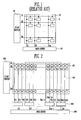
- FIG. 1 is a schematic view showing a conventional organic electroluminescence display device.
- the organic electroluminescence display device includes a pixel unit 10, a data driver 20 and a scan driver 30.
- the pixel unit 10 has a plurality of pixels 11 arranged therein, and organic light emitting elements (not shown) connected to each of the pixels 11.
- the pixel unit has a plurality of scan lines (S1,S2,...Sn-1,Sn) arranged in a horizontal direction for transmitting a scan signal, and a plurality of data lines (D1, D2,....Dm-1, Dm) arranged in a vertical direction for transmitting a data signal.
- the pixel unit 10 displays an image by allowing the luminous elements to emit the lights according to the scan signal and the data signal.
- the data driver 20 is a unit for applying a data signal to the pixel unit 10, and is connected to the data lines (D1, D2,....Dm-1, Dm).
- a plurality of channels (not shown), to which the data signal is outputted, are connected to the data lines (D1, D2,....Dm-1, Dm), and one data line is connected to one channel.
- the scan driver 30 is a unit sequentially outputting a scan signal and is connected to the scan lines (S1,S2,...Sn-1,Sn) in order to supply the scan signal to a specific row of the pixel unit 10.
- the data signal inputted in the data driver 20 is applied to a specific row of the pixel unit 10 to which the scan signal is supplied in order to display an image, and one frame is completed if all rows are sequentially selected.
- each of the pixels connected to the same scan line are connected to different data lines, and therefore the wires become complicated as the number of the data lines connected to the pixel unit increase. Also, if the number of the data lines increases, then the channel number of the data drivers also increases and a size of the data driver is enlarged, therefore increasing the entire cost of the device.
- the previous data signals are stored in the data lines, and an image may deteriorate since a deviation occurs in an electric current flowing in the pixels.
- an aspect of the present invention is to provide an organic electroluminescence display device capable of reducing a size of a data driver by reducing the number of channels of the data driver, and also reducing a deviation of electric current flowing in pixels by resetting the data lines, and a driving method for the same.
- An aspect of the present invention is achieved by providing an organic electroluminescence display device as set out in Claim 1. Preferred features of this aspect are set out in claims 2 to 13. According to a second aspect of the invention, there is provided a method as set out in Claim 14. Preferred features of this aspect are set out in claims 15 and 16.
- FIG. 2 is a schematic view showing an organic electroluminescence display device according to an embodiment of the present invention.
- the organic electroluminescence display device includes a pixel unit 100, a data driver 200, a MUX unit 300 and a scan driver 400.
- the pixel unit 100 has a plurality of pixels 101 arranged therein and an organic light emitting diode (not shown) connected to each of the pixels 101.
- the pixel unit 100 has a plurality of scan lines (S1, S2,...Sn-1,Sn) formed in a horizontal direction and supplying a scan signal, and a plurality of data lines (D11, D12,D13,....Dm1,Dm2, Dm3) formed in a vertical direction and supplying a data signal.
- the pixel unit 100 displays an image by allowing the organic light emitting diode to emit the light according to the scan signal and the data signal.
- the data driver 200 is a unit for applying the data signal to the pixel unit 100, and has a plurality of channels (D1, D2,....Dm-1, Dm) for outputting the data signal to each of the channels.
- a size of the data driver 200 can be reduced compared to conventional arrangements since red, green, and blue data are sequentially outputted in one channel, thus lowering the number of channels of the data driver 200 when compared to the number of the data lines (D11, D12,D13,....Dm1,Dm2, Dm3) of the pixel unit 100.
- the data driver 200 can reset the data lines (D11, D12,D13,....Dm1,Dm2, Dm3) by outputting the reset signal in each of the channels (D1, D2,....Dm-1, Dm).
- the MUX unit 300 is connected between the data lines (D11, D12, D13,....Dm1,Dm2, Dm3) and the channels (D1, D2,....Dm-1, Dm) to sequentially supply red, green and blue data signals, outputted through one channel, corresponding to the three data lines, and also the MUX unit 300 supplies the reset signal, outputted in the channels, to the three data lines so as to reset the data lines.
- the scan driver 400 is a unit sequentially outputting a scan signal and connected to the scan lines (S1,S2,...Sn-1,Sn), and supplies the scan signal to a specific row of the pixel unit 100.
- the data signal inputted in the data driver 200 is applied to the specific row of the pixel unit 100 to which the scan signal is supplied to display an image, and one frame is completed if all rows are sequentially selected.
- FIG. 3 is a schematic view showing an organic electroluminescence display device according to another embodiment of the present invention.
- the organic electroluminescence display device includes a pixel unit 100, a data driver 200, a MUX unit 300, a reset unit 320 and a scan driver 400.
- the pixel unit 100 has a plurality of pixels 101 arranged therein and an organic light emitting diode (not shown) connected to each of the pixels 101.
- the pixel unit 100 has a plurality of scan lines (S1,S2,...Sn-1,Sn) formed in a horizontal direction and supplying a scan signal, and a plurality of data lines (D11, D12,D13,....Dm1,Dm2, Dm3) formed in a vertical direction and supplying a data signal.
- the pixel unit 100 displays an image by allowing the organic light emitting diode to emit the light according to the scan signal and the data signal.
- the data driver 200 applies the data signal to the pixel unit 100, and has a plurality of channels (D1, D2,....Dm-1, Dm) for outputting the data signal to each of the channels.
- a size of the data driver 200 is reduced since red, green, and blue data is sequentially outputted in one channel, thus lowering the channel number of the data driver 200 compared to the number of the data lines (D11, D12,D13,....Dm1,Dm2, Dm3) of the pixel unit 100.
- the MUX unit 300 is connected between the data lines (D11, D12,D13,....Dm1,Dm2, Dm3) and the channels (D1, D2,....Dm-1, Dm) and sequentially supplies red, green and blue data signals, outputted through one channel, to the corresponding three data lines so as to reduce the channel number of the data drivers 200.
- the reset unit 320 is connected to an output terminal of the MUX unit 300 and includes a reset line for supplying a reset signal; and a reset control line controlling the reset unit.
- the reset unit 320 is reset by supplying the reset signal, supplied to the reset control line through the reset line, to the data lines (D11, D12,D13,....Dm1,Dm2, Dm3).
- the scan driver 400 is a unit sequentially outputting a scan signal and connected to the scan lines (S1,S2,...Sn-1,Sn) and supplying the scan signal to a specific row of the pixel unit 100.
- the data signal inputted in the data driver 200 is applied to the specific row of the pixel unit 100 to which the scan signal is supplied to display an image, and one frame is completed if all rows are sequentially selected.
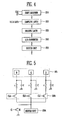
- FIG. 4 is a schematic view showing a data driver used in the organic electroluminescence display device as shown in FIG. 2.
- the data driver 200 includes a shift resistor 210, a sampling latch 220, a holding latch 230, a D/A converter 240 and a buffer unit 250.
- the shift resistor 210 sequentially shifts a start pulse (SP) according to a clock signal (CLK) to generate a sampling signal, thereby applying the generated sampling signal to the sampling latch 220.
- SP start pulse
- CLK clock signal
- the sampling latch 220 receives the sampling signal outputted from the shift resistor 210, and then stores a digital data signal inputted in series from the outside according to the sampling signal.
- the holding latch 230 receives the digital data signal; stored in the sampling latch 220, depending on a holding signal (DH) supplied from the outside, holds the received digital data signal during a first horizontal period, and then outputs the digital signal.
- DH holding signal
- the D/A converter 240 receives the digital data signal and converts the received digital data signal to an analog data signal, and outputs a voltage corresponding to each of the grey levels.
- the buffer unit 250 is a unit amplifying and outputting the analog data signal, and prevents the data signal from being distorted by a load of the data lines.
- An output terminal of the buffer unit 250 may be referred to as a channel, and the analog data signal is outputted to every channel.
- FIG. 5 is a circuit view showing a connection relation between a data driver and a MUX unit in the organic electroluminescence display device as shown in FIG. 2.
- pixels 101i represented by R, G and B; data lines connected to each of the pixels; a MUX unit 300i connected to the data lines; a buffer unit 250i of the data driver; and a reset transistor (Mi) connected to the buffer unit 250i are sequentially connected to each other.
- “r” and "C” represent a line resistance and a parasitic capacitor of the data line, respectively.
- the reset transistor (Mi) has a source connected to the data lines; a drain connected to the ground power source; and a gate connected to the reset signal line (CI). Therefore, the reset transistor (Mi) can reset the voltage of the data lines through the voltage of the ground power source by carrying out a switching operation according to the reset signal line (CI).
- the source may be referred to as a first electrode
- the drain may be referred to as a second electrode
- the gate may be referred to as a third electrode.
- a R data signal outputted from the buffer unit 250i is supplied to a R pixel through the MUX unit 300i, a G data signal is supplied to a G pixel through the MUX unit 300i, and a B data signal is supplied to a B pixel through the MUX unit 300i. Accordingly, the R data signal, the G data signal and the B data signal are stored in the data lines, respectively. Furthermore, if the buffer unit 250i is disconnected from the data lines, then the reset transistor (Mi) is in a turned-on state through the reset control signal, supplying the ground power source to the data lines. Accordingly, the data lines are reset by the ground power source.
- the ground power source uses a ground.
- FIG. 6 is a circuit view showing a connection relation between a data driver and a MUX unit in the organic electroluminescence display device as shown in FIG. 3.
- FIG. 6 there is shown the connection relation of pixels 101i represented by R, G and B; data lines connected to each of the pixels; a reset unit 320i connected to the data lines; a MUX unit 300i connected to the data lines; a buffer unit 250i of the data driver; and reset transistors (Mr), (Mb) and (Mg) connected to the buffer unit 250i.
- “r” and “C” represent a line resistance and a parasitic capacitor of the data line, respectively.
- the reset unit 320i includes a first transistor (Mr) having a first electrode connected to the red data line, a second electrode connected to the ground power source (GND) and a gate connected to the reset control signal line (CI); a second transistor (Mb) having a first electrode connected to the green data line, a second electrode connected to the ground power source (GND) and a gate connected to the reset control signal line (CI); and a third transistor (Mg) having a first electrode connected to the blue data line, a second electrode connected to the ground power source (GND) and a gate connected to the reset control signal line (CI).
- a R data signal outputted from the buffer unit 250i is supplied to an R pixel through the MUX unit 300i, a G data signal is supplied to a G pixel through the MUX unit 300i, and a B data signal is supplied to a B pixel through the MUX unit 300i. Accordingly, the R data signal, the G data signal and the B data signal are stored in the data lines, respectively.
- the ground power source is supplied to the data lines to reset the data lines through the ground power source.
- the reset signal uses a ground.
- FIG. 7 is a diagram showing a voltage of a data line in the organic electroluminescence display device as shown in FIG. 2.
- the horizontal axis represents a time
- the principal axis represents a voltage of the data line. If the reset signal is applied when a voltage of 4V is charged in the data lines, a voltage of the data signal approaches a voltage of 0V when a voltage of the data line drops for a time of 4 ⁇ s.
- FIG. 8 is a diagram showing a voltage of a data line in the organic electroluminescence display device as shown in FIG. 3.
- the horizontal axis represents a time
- the principal axis represents a voltage of a data line.
- "a” is a graph showing a voltage change of the data line arranged in a central region of the pixel unit
- "b” is a graph showing a voltage change of the data line arranged in an edge of the pixel unit.
- the organic electroluminescence display device and the driving method for the same are useful in reducing a size of a data driver by connecting a plurality of data lines to one channel of the data driver through a MUX unit to reduce the number of the data lines, as well as to reduce a deviation of electric current flowing in pixels by resetting the data lines.
Landscapes
- Engineering & Computer Science (AREA)
- Physics & Mathematics (AREA)
- Computer Hardware Design (AREA)
- General Physics & Mathematics (AREA)
- Theoretical Computer Science (AREA)
- Electroluminescent Light Sources (AREA)
- Control Of El Displays (AREA)
- Control Of Indicators Other Than Cathode Ray Tubes (AREA)
Abstract
Description
- The present invention relates to an organic electroluminescence display device and a driving method for the same, and more particularly to an organic electroluminescence display device capable of reducing a deviation of electric current flowing in pixels by resetting a data signal stored in data lines, and a driving method for the same.
- In recent years, there has been much development in the field of flat panel displays which are more lightweight and have a smaller volume than a cathode ray tube. Currently, flat panel displays include a display region in which a plurality of pixels are arranged in a matrix form on a substrate, and an image is displayed by connecting scan lines and data lines to each of the pixels to selectively apply a data signal to the pixels.
- Flat panel displays are classified into a passive matrix type light emitting display and an active matrix type light emitting display, depending on the driving systems of the pixels. An active matrix type light emitting display which selectively turns on the light in every unit pixel has been widely used due to its superior resolution, contrast, and response time.
- Flat panel displays are used as displays or monitors in apparatuses such as personal computers, mobile phones, PDA's, etc., and LCD's using a liquid crystal panel, an organic electroluminescence display device using an organic light emitting diode, PDP's using a plasma panel and the like have been widely known in the art. Organic electroluminescence display devices are known to have excellent luminous efficiency, luminance and viewing angle and a rapid response time.
- FIG. 1 is a schematic view showing a conventional organic electroluminescence display device. Referring to FIG. 1, the organic electroluminescence display device includes a
pixel unit 10, adata driver 20 and ascan driver 30. - The
pixel unit 10 has a plurality ofpixels 11 arranged therein, and organic light emitting elements (not shown) connected to each of thepixels 11. The pixel unit has a plurality of scan lines (S1,S2,...Sn-1,Sn) arranged in a horizontal direction for transmitting a scan signal, and a plurality of data lines (D1, D2,....Dm-1, Dm) arranged in a vertical direction for transmitting a data signal. Thepixel unit 10 displays an image by allowing the luminous elements to emit the lights according to the scan signal and the data signal. - The
data driver 20 is a unit for applying a data signal to thepixel unit 10, and is connected to the data lines (D1, D2,....Dm-1, Dm). In thedata driver 20, a plurality of channels (not shown), to which the data signal is outputted, are connected to the data lines (D1, D2,....Dm-1, Dm), and one data line is connected to one channel. - The
scan driver 30 is a unit sequentially outputting a scan signal and is connected to the scan lines (S1,S2,...Sn-1,Sn) in order to supply the scan signal to a specific row of thepixel unit 10. The data signal inputted in thedata driver 20 is applied to a specific row of thepixel unit 10 to which the scan signal is supplied in order to display an image, and one frame is completed if all rows are sequentially selected. - In the organic electroluminescence display device as configured above, each of the pixels connected to the same scan line are connected to different data lines, and therefore the wires become complicated as the number of the data lines connected to the pixel unit increase. Also, if the number of the data lines increases, then the channel number of the data drivers also increases and a size of the data driver is enlarged, therefore increasing the entire cost of the device.
- Also, the previous data signals are stored in the data lines, and an image may deteriorate since a deviation occurs in an electric current flowing in the pixels.
- Accordingly, aspects of the present invention are designed to solve such drawbacks of the related are art and/or other drawbacks, and therefore an aspect of the present invention is to provide an organic electroluminescence display device capable of reducing a size of a data driver by reducing the number of channels of the data driver, and also reducing a deviation of electric current flowing in pixels by resetting the data lines, and a driving method for the same.
- An aspect of the present invention is achieved by providing an organic electroluminescence display device as set out in
Claim 1. Preferred features of this aspect are set out inclaims 2 to 13. According to a second aspect of the invention, there is provided a method as set out in Claim 14. Preferred features of this aspect are set out in claims 15 and 16. - Additional aspects and/or advantages of the invention will be set forth in part in the description which follows and, in part, will be obvious from the description, or may be learned by practice of the invention.
- These and/or other aspects and advantages of the invention will become apparent and more readily appreciated from the following description of the embodiments, taken in conjunction with the accompanying drawings of which:
- FIG. 1 is a schematic view showing a conventional organic electroluminescence display device.
- FIG. 2 is a schematic view showing an organic electroluminescence display device according to an aspect of the present invention.
- FIG. 3 is a schematic view showing an organic electroluminescence display device according to an aspect of the present invention.
- FIG. 4 is a schematic view showing a data driver used in the organic electroluminescence display device as shown in FIG. 2.
- FIG. 5 is a circuit view showing a connection relation between a data driver and a MUX unit in the organic electroluminescence display device shown in FIG. 2.
- FIG. 6 is a circuit view showing a connection relation between a data driver and a MUX unit in the organic electroluminescence display device shown in FIG. 3.
- FIG. 7 is a diagram showing a voltage of a data line in the organic electroluminescence display device shown in FIG. 2.
- FIG. 8 is a diagram showing a voltage of a data line in the organic electroluminescence display device shown in FIG. 3.
- Reference will now be made in detail to the present embodiments of the present invention, examples of which are illustrated in the accompanying drawings, wherein like reference numerals refer to the like elements throughout. The embodiments are described below in order to explain the present invention by referring to the figures.
- FIG. 2 is a schematic view showing an organic electroluminescence display device according to an embodiment of the present invention. Referring to FIG. 2, the organic electroluminescence display device includes a
pixel unit 100, adata driver 200, aMUX unit 300 and ascan driver 400. - The
pixel unit 100 has a plurality ofpixels 101 arranged therein and an organic light emitting diode (not shown) connected to each of thepixels 101. Thepixel unit 100 has a plurality of scan lines (S1, S2,...Sn-1,Sn) formed in a horizontal direction and supplying a scan signal, and a plurality of data lines (D11, D12,D13,....Dm1,Dm2, Dm3) formed in a vertical direction and supplying a data signal. Thepixel unit 100 displays an image by allowing the organic light emitting diode to emit the light according to the scan signal and the data signal. - The
data driver 200 is a unit for applying the data signal to thepixel unit 100, and has a plurality of channels (D1, D2,....Dm-1, Dm) for outputting the data signal to each of the channels. A size of thedata driver 200 can be reduced compared to conventional arrangements since red, green, and blue data are sequentially outputted in one channel, thus lowering the number of channels of thedata driver 200 when compared to the number of the data lines (D11, D12,D13,....Dm1,Dm2, Dm3) of thepixel unit 100. Also, thedata driver 200 can reset the data lines (D11, D12,D13,....Dm1,Dm2, Dm3) by outputting the reset signal in each of the channels (D1, D2,....Dm-1, Dm). - The
MUX unit 300 is connected between the data lines (D11, D12, D13,....Dm1,Dm2, Dm3) and the channels (D1, D2,....Dm-1, Dm) to sequentially supply red, green and blue data signals, outputted through one channel, corresponding to the three data lines, and also theMUX unit 300 supplies the reset signal, outputted in the channels, to the three data lines so as to reset the data lines. - The
scan driver 400 is a unit sequentially outputting a scan signal and connected to the scan lines (S1,S2,...Sn-1,Sn), and supplies the scan signal to a specific row of thepixel unit 100. The data signal inputted in thedata driver 200 is applied to the specific row of thepixel unit 100 to which the scan signal is supplied to display an image, and one frame is completed if all rows are sequentially selected. - FIG. 3 is a schematic view showing an organic electroluminescence display device according to another embodiment of the present invention. Referring to FIG. 3, the organic electroluminescence display device includes a
pixel unit 100, adata driver 200, aMUX unit 300, areset unit 320 and ascan driver 400. - The
pixel unit 100 has a plurality ofpixels 101 arranged therein and an organic light emitting diode (not shown) connected to each of thepixels 101. Thepixel unit 100 has a plurality of scan lines (S1,S2,...Sn-1,Sn) formed in a horizontal direction and supplying a scan signal, and a plurality of data lines (D11, D12,D13,....Dm1,Dm2, Dm3) formed in a vertical direction and supplying a data signal. Thepixel unit 100 displays an image by allowing the organic light emitting diode to emit the light according to the scan signal and the data signal. - The
data driver 200 applies the data signal to thepixel unit 100, and has a plurality of channels (D1, D2,....Dm-1, Dm) for outputting the data signal to each of the channels. A size of thedata driver 200 is reduced since red, green, and blue data is sequentially outputted in one channel, thus lowering the channel number of thedata driver 200 compared to the number of the data lines (D11, D12,D13,....Dm1,Dm2, Dm3) of thepixel unit 100. - The
MUX unit 300 is connected between the data lines (D11, D12,D13,....Dm1,Dm2, Dm3) and the channels (D1, D2,....Dm-1, Dm) and sequentially supplies red, green and blue data signals, outputted through one channel, to the corresponding three data lines so as to reduce the channel number of thedata drivers 200. - The
reset unit 320 is connected to an output terminal of theMUX unit 300 and includes a reset line for supplying a reset signal; and a reset control line controlling the reset unit. Thereset unit 320 is reset by supplying the reset signal, supplied to the reset control line through the reset line, to the data lines (D11, D12,D13,....Dm1,Dm2, Dm3). - The
scan driver 400 is a unit sequentially outputting a scan signal and connected to the scan lines (S1,S2,...Sn-1,Sn) and supplying the scan signal to a specific row of thepixel unit 100. The data signal inputted in thedata driver 200 is applied to the specific row of thepixel unit 100 to which the scan signal is supplied to display an image, and one frame is completed if all rows are sequentially selected. - FIG. 4 is a schematic view showing a data driver used in the organic electroluminescence display device as shown in FIG. 2. Referring to FIG. 4, the
data driver 200 includes ashift resistor 210, asampling latch 220, a holdinglatch 230, a D/A converter 240 and abuffer unit 250. - The
shift resistor 210 sequentially shifts a start pulse (SP) according to a clock signal (CLK) to generate a sampling signal, thereby applying the generated sampling signal to thesampling latch 220. - The
sampling latch 220 receives the sampling signal outputted from theshift resistor 210, and then stores a digital data signal inputted in series from the outside according to the sampling signal. - The holding
latch 230 receives the digital data signal; stored in thesampling latch 220, depending on a holding signal (DH) supplied from the outside, holds the received digital data signal during a first horizontal period, and then outputs the digital signal. - The D/
A converter 240 receives the digital data signal and converts the received digital data signal to an analog data signal, and outputs a voltage corresponding to each of the grey levels. - The
buffer unit 250 is a unit amplifying and outputting the analog data signal, and prevents the data signal from being distorted by a load of the data lines. An output terminal of thebuffer unit 250 may be referred to as a channel, and the analog data signal is outputted to every channel. - FIG. 5 is a circuit view showing a connection relation between a data driver and a MUX unit in the organic electroluminescence display device as shown in FIG. 2. Referring to FIG. 5, there is shown
pixels 101i represented by R, G and B; data lines connected to each of the pixels; aMUX unit 300i connected to the data lines; abuffer unit 250i of the data driver; and a reset transistor (Mi) connected to thebuffer unit 250i are sequentially connected to each other. Additionally, "r" and "C" represent a line resistance and a parasitic capacitor of the data line, respectively. - The reset transistor (Mi) has a source connected to the data lines; a drain connected to the ground power source; and a gate connected to the reset signal line (CI). Therefore, the reset transistor (Mi) can reset the voltage of the data lines through the voltage of the ground power source by carrying out a switching operation according to the reset signal line (CI). Here, the source may be referred to as a first electrode, the drain may be referred to as a second electrode, and the gate may be referred to as a third electrode.
- Referring to an operation of the reset transistor (Mi), a R data signal outputted from the
buffer unit 250i is supplied to a R pixel through theMUX unit 300i, a G data signal is supplied to a G pixel through theMUX unit 300i, and a B data signal is supplied to a B pixel through theMUX unit 300i. Accordingly, the R data signal, the G data signal and the B data signal are stored in the data lines, respectively. Furthermore, if thebuffer unit 250i is disconnected from the data lines, then the reset transistor (Mi) is in a turned-on state through the reset control signal, supplying the ground power source to the data lines. Accordingly, the data lines are reset by the ground power source. The ground power source uses a ground. - FIG. 6 is a circuit view showing a connection relation between a data driver and a MUX unit in the organic electroluminescence display device as shown in FIG. 3. Referring to FIG. 6, there is shown the connection relation of
pixels 101i represented by R, G and B; data lines connected to each of the pixels; areset unit 320i connected to the data lines; aMUX unit 300i connected to the data lines; abuffer unit 250i of the data driver; and reset transistors (Mr), (Mb) and (Mg) connected to thebuffer unit 250i. Also, "r" and "C" represent a line resistance and a parasitic capacitor of the data line, respectively. - The
reset unit 320i includes a first transistor (Mr) having a first electrode connected to the red data line, a second electrode connected to the ground power source (GND) and a gate connected to the reset control signal line (CI); a second transistor (Mb) having a first electrode connected to the green data line, a second electrode connected to the ground power source (GND) and a gate connected to the reset control signal line (CI); and a third transistor (Mg) having a first electrode connected to the blue data line, a second electrode connected to the ground power source (GND) and a gate connected to the reset control signal line (CI). - Referring to an operation of the reset transistors (Mr), (Mb) and (Mg), a R data signal outputted from the
buffer unit 250i is supplied to an R pixel through theMUX unit 300i, a G data signal is supplied to a G pixel through theMUX unit 300i, and a B data signal is supplied to a B pixel through theMUX unit 300i. Accordingly, the R data signal, the G data signal and the B data signal are stored in the data lines, respectively. And, if the first transistor (Mr), the second transistor (Mb) and the third transistor (Mg) are in a turned-on state by the reset control signal and the connection relation between the data line and theMUX unit 300i is in a turned-off state, then the ground power source is supplied to the data lines to reset the data lines through the ground power source. The reset signal uses a ground. - FIG. 7 is a diagram showing a voltage of a data line in the organic electroluminescence display device as shown in FIG. 2. Referring to FIG. 7, the horizontal axis represents a time, and the principal axis represents a voltage of the data line. If the reset signal is applied when a voltage of 4V is charged in the data lines, a voltage of the data signal approaches a voltage of 0V when a voltage of the data line drops for a time of 4µs.
- FIG. 8 is a diagram showing a voltage of a data line in the organic electroluminescence display device as shown in FIG. 3. Referring to FIG. 8, the horizontal axis represents a time, and the principal axis represents a voltage of a data line. And, "a" is a graph showing a voltage change of the data line arranged in a central region of the pixel unit, and "b" is a graph showing a voltage change of the data line arranged in an edge of the pixel unit.
- Comparing "a" with "b", it might seem that the data line arranged in a central region of the pixel unit is reset at a more rapid rate than the data line arranged in an edge of the pixel unit.
- As described above, the organic electroluminescence display device and the driving method for the same according to embodiments of the present invention are useful in reducing a size of a data driver by connecting a plurality of data lines to one channel of the data driver through a MUX unit to reduce the number of the data lines, as well as to reduce a deviation of electric current flowing in pixels by resetting the data lines.
- Although a few embodiments of the present invention have been shown and described, it would be appreciated by those skilled in the art that changes may be made in this embodiment without departing from the principles of the invention, the scope of which is defined in the claims and their equivalents.
Claims (15)
- An organic electroluminescence display device comprising:a pixel unit including a plurality of pixels defined by data lines and scan lines arranged to display an image to correspond to a data signal and a scan signal;a data driver arranged to generate the data signal and to supply the data signal to the pixel unit through a plurality of channels;a MUX unit connected to the data lines arranged to output the data signals from the data driver and to selectively supply the data signal to the data lines;a scan driver arranged to generate a scan signal and to supply the generated scan signal to the pixel unit; andreset means arranged to supply a reset signal to the data lines.
- An organic electroluminescence display device according to claim 1, wherein the reset means comprises a reset signal transmitting unit arranged to supply the reset signal, the reset signal transmitting unit being connected to the channels of the data driver and being arranged provide the reset signal to the data lines through the MUX unit.
- An organic electroluminescence display device according to claim 2, wherein the reset signal transmitting unit has a first electrode connected to one of the channels; a second electrode connected to a ground power source; and a gate to which a reset control signal is provided, and includes a reset transistor supplying the ground power source to the MUX unit according to the reset control signal to provide the reset signal.
- An organic electroluminescence display device according to any one of claims 1 or 2, wherein the data driver comprises:a reset transistor connected to each of the channels for switching a ground power source to supply a ground power source to the MUX unit.
- An organic electroluminescence display device according to any one of claims 2 to 4, wherein the channels are in a turned-off state when the reset signal is supplied to the data lines through the reset signal transmitting unit.
- An organic electroluminescence display device according to claim 1, wherein the reset means comprises:a reset unit connected to the data lines arranged to supply a ground power source to the data lines.
- An organic electroluminescence display device according claims 6, wherein the reset unit comprises:a first transistor having a first electrode connected to the data lines to which red data is supplied; a second electrode connected to the ground power source; and a gate connected to a control signal line;a second transistor having a first electrode connected to the data lines to which green data is supplied; a second electrode connected to the ground power source; and a gate connected to the control signal line; anda third transistor having a first electrode connected to the data lines to which blue data is supplied; a second electrode connected to the ground power source; and a gate connected to the control signal line.
- An organic electroluminescence display device according to claims 6 or 7, wherein the channels are in a turned-off state when a reset signal is supplied to the data lines through the reset unit.
- An organic electroluminescence display device according to any one of claims 1 to 8, wherein the MUX unit including a plurality of multiplexers, each multiplexer being connected to three data lines and to one channel, wherein each multiplexer is arranged to output the data signal from the data driver to the three data lines.
- An organic electroluminescent display device according to claim 8 or 9, wherein each channel of the data driver is arranged to apply the data signal to three data lines of the MUX unit.
- An organic electroluminescence display device according to any one of claims 8 to 10, wherein the three data lines include a red data line, a green data line and a blue data line.
- An organic electroluminescence display device according to any one of claims 1 to 11, wherein the reset means includes a plurality of reset transistors connected to the data lines.
- A method of driving an organic electroluminescence display device that resets data lines using a reset signal, comprising:generating a data signal and supplying the generated data signal to data lines; andinterrupting the data signal and supplying the reset signal to the data lines.
- A method of driving an organic electroluminescence display device according to claim 13, wherein the reset signal uses a ground.
- A method of driving an organic electroluminescence display device according to claim 13 or 14, wherein the generated data signal is supplied to one of three data lines of the pixel electrode.
Applications Claiming Priority (1)
| Application Number | Priority Date | Filing Date | Title |
|---|---|---|---|
| KR1020060088641A KR100796136B1 (en) | 2006-09-13 | 2006-09-13 | Organic light emitting display device and driving method thereof |
Publications (2)
| Publication Number | Publication Date |
|---|---|
| EP1901275A2 true EP1901275A2 (en) | 2008-03-19 |
| EP1901275A3 EP1901275A3 (en) | 2009-09-09 |
Family
ID=38683612
Family Applications (1)
| Application Number | Title | Priority Date | Filing Date |
|---|---|---|---|
| EP07253642A Withdrawn EP1901275A3 (en) | 2006-09-13 | 2007-09-13 | Data driver for organic electro luminescence display device and driving method for the same |
Country Status (5)
| Country | Link |
|---|---|
| US (1) | US20080062089A1 (en) |
| EP (1) | EP1901275A3 (en) |
| JP (1) | JP2008070849A (en) |
| KR (1) | KR100796136B1 (en) |
| CN (1) | CN101145318A (en) |
Families Citing this family (33)
| Publication number | Priority date | Publication date | Assignee | Title |
|---|---|---|---|---|
| TWI365437B (en) * | 2007-05-09 | 2012-06-01 | Himax Tech Ltd | Reset circuit for power-on and power-off |
| US20090219233A1 (en) * | 2008-03-03 | 2009-09-03 | Park Yong-Sung | Organic light emitting display and method of driving the same |
| KR101073206B1 (en) | 2010-01-05 | 2011-10-12 | 삼성모바일디스플레이주식회사 | Organic Light Emitting Display Device |
| CN102646389B (en) * | 2011-09-09 | 2014-07-23 | 京东方科技集团股份有限公司 | Organic light emitting diode (OLED) panel and OLED panel driving method |
| CN102621758B (en) * | 2012-04-16 | 2015-07-01 | 深圳市华星光电技术有限公司 | Liquid crystal display device and driving circuit thereof |
| KR102071566B1 (en) * | 2013-02-27 | 2020-03-03 | 삼성디스플레이 주식회사 | Organic light emitting display device and driving method thereof |
| KR102137079B1 (en) * | 2014-03-03 | 2020-07-24 | 삼성디스플레이 주식회사 | Organic light emitting display device |
| KR20150112620A (en) * | 2014-03-28 | 2015-10-07 | 삼성전자주식회사 | Dispaly apparatus, display system and controlling method thereof |
| CN103927987B (en) * | 2014-04-02 | 2015-12-09 | 京东方科技集团股份有限公司 | Image element circuit and display device |
| CN104036747A (en) * | 2014-06-13 | 2014-09-10 | 深圳市华星光电技术有限公司 | Electronic device capable of reducing number of driver chips |
| CN104049931B (en) * | 2014-06-17 | 2017-05-03 | 佛山市顺德区美的电热电器制造有限公司 | Reset displaying device, reset displaying method and cooking heating equipment |
| KR102317450B1 (en) * | 2014-11-10 | 2021-10-28 | 삼성디스플레이 주식회사 | Organic Light Emitting Display Device and Driving Method Thereof |
| CN104503612B (en) | 2014-12-12 | 2017-11-10 | 上海天马微电子有限公司 | Touch display panel and electronic equipment |
| CN105810143B (en) * | 2014-12-29 | 2018-09-28 | 昆山工研院新型平板显示技术中心有限公司 | A kind of data drive circuit and its driving method and organic light emitting display |
| US10147360B2 (en) * | 2015-03-31 | 2018-12-04 | Universal Display Corporation | Rugged display device architecture |
| CN106847181A (en) * | 2015-12-07 | 2017-06-13 | 上海和辉光电有限公司 | Data wire to pel array enters the device and method of line precharge |
| CN105609049B (en) * | 2015-12-31 | 2017-07-21 | 京东方科技集团股份有限公司 | Display driver circuit, array base palte, circuit drive method and display device |
| JP6828247B2 (en) | 2016-02-19 | 2021-02-10 | セイコーエプソン株式会社 | Display devices and electronic devices |
| CN105761675B (en) * | 2016-05-18 | 2018-03-20 | 上海天马微电子有限公司 | Organic light emitting display panel, driving method thereof and organic light emitting display device |
| CN106297708A (en) * | 2016-09-08 | 2017-01-04 | 武汉华星光电技术有限公司 | A kind of method reducing display panels display inequality |
| CN107240374A (en) * | 2017-07-21 | 2017-10-10 | 京东方科技集团股份有限公司 | A kind of source electrode drive circuit, display device and its driving method |
| KR102459706B1 (en) * | 2017-09-13 | 2022-10-28 | 엘지디스플레이 주식회사 | Organic Light Emitting Display Using a Multiplexer |
| CN108447445B (en) * | 2018-03-30 | 2020-02-28 | 京东方科技集团股份有限公司 | Pixel circuit, display panel and driving method thereof |
| CN108399880B (en) * | 2018-04-19 | 2019-08-02 | 武汉华星光电半导体显示技术有限公司 | Test circuit, array substrate and luminous display unit |
| US10573210B2 (en) | 2018-04-19 | 2020-02-25 | Wuhan China Star Optoelectronics Semiconductor Display Technology Co., Ltd. | Test circuit, array substrate, and light-emitting display apparatus |
| TWI707327B (en) * | 2018-12-07 | 2020-10-11 | 友達光電股份有限公司 | Driving circuit, backlight module, display module, and driving method |
| CN109669292A (en) | 2019-01-04 | 2019-04-23 | 京东方科技集团股份有限公司 | A kind of display panel and display device |
| TWI696163B (en) * | 2019-03-25 | 2020-06-11 | 友達光電股份有限公司 | Control circuit |
| CN110853576B (en) * | 2019-11-20 | 2021-03-23 | 京东方科技集团股份有限公司 | Display substrate and display device |
| CN111354309A (en) * | 2020-04-15 | 2020-06-30 | 京东方科技集团股份有限公司 | Display driving module, display driving method and display device |
| KR102791100B1 (en) * | 2020-08-03 | 2025-04-08 | 삼성디스플레이 주식회사 | Diplay device |
| CN114863873B (en) * | 2022-04-29 | 2023-07-21 | 武汉天马微电子有限公司 | Display panel and display device |
| CN116106427A (en) * | 2023-01-18 | 2023-05-12 | 京东方科技集团股份有限公司 | An ultrasonic monitoring device and its driving method |
Family Cites Families (16)
| Publication number | Priority date | Publication date | Assignee | Title |
|---|---|---|---|---|
| JP4027614B2 (en) * | 2001-03-28 | 2007-12-26 | 株式会社日立製作所 | Display device |
| US20030103022A1 (en) * | 2001-11-09 | 2003-06-05 | Yukihiro Noguchi | Display apparatus with function for initializing luminance data of optical element |
| KR100649243B1 (en) * | 2002-03-21 | 2006-11-24 | 삼성에스디아이 주식회사 | Organic electroluminescent display and driving method thereof |
| KR100956463B1 (en) * | 2002-04-26 | 2010-05-10 | 도시바 모바일 디스플레이 가부시키가이샤 | EL display |
| JP3882796B2 (en) * | 2003-07-22 | 2007-02-21 | セイコーエプソン株式会社 | Electro-optical device, driving method of electro-optical device, and electronic apparatus |
| JP4176688B2 (en) * | 2003-09-17 | 2008-11-05 | シャープ株式会社 | Display device and driving method thereof |
| JPWO2005043915A1 (en) * | 2003-10-31 | 2007-05-10 | 株式会社Kddiメディアウィル | Video analysis device and video failure detection device |
| KR100578913B1 (en) * | 2003-11-27 | 2006-05-11 | 삼성에스디아이 주식회사 | Display device using demultiplexer and driving method thereof |
| US8115705B2 (en) * | 2004-05-17 | 2012-02-14 | Global Oled Technology Llc | Display device |
| JP2006053347A (en) * | 2004-08-11 | 2006-02-23 | Eastman Kodak Co | Display apparatus |
| KR100581810B1 (en) * | 2004-08-25 | 2006-05-23 | 삼성에스디아이 주식회사 | Light emitting display device and driving method thereof |
| KR100581809B1 (en) * | 2004-08-25 | 2006-05-23 | 삼성에스디아이 주식회사 | Demultiplexing circuit and light emitting display device using the same |
| JP4290627B2 (en) * | 2004-10-04 | 2009-07-08 | シャープ株式会社 | Display element driving apparatus, display device including the display element driving apparatus, and display element driving method |
| KR100604053B1 (en) * | 2004-10-13 | 2006-07-24 | 삼성에스디아이 주식회사 | Light emitting display |
| KR100604060B1 (en) * | 2004-12-08 | 2006-07-24 | 삼성에스디아이 주식회사 | Light emitting display device and driving method thereof |
| JP2006301166A (en) * | 2005-04-19 | 2006-11-02 | Hitachi Displays Ltd | Display device and driving method thereof |
-
2006
- 2006-09-13 KR KR1020060088641A patent/KR100796136B1/en not_active Expired - Fee Related
- 2006-11-10 JP JP2006305694A patent/JP2008070849A/en active Pending
-
2007
- 2007-03-20 US US11/688,365 patent/US20080062089A1/en not_active Abandoned
- 2007-09-13 EP EP07253642A patent/EP1901275A3/en not_active Withdrawn
- 2007-09-13 CN CNA200710145700XA patent/CN101145318A/en active Pending
Non-Patent Citations (1)
| Title |
|---|
| None |
Also Published As
| Publication number | Publication date |
|---|---|
| EP1901275A3 (en) | 2009-09-09 |
| US20080062089A1 (en) | 2008-03-13 |
| CN101145318A (en) | 2008-03-19 |
| JP2008070849A (en) | 2008-03-27 |
| KR100796136B1 (en) | 2008-01-21 |
Similar Documents
| Publication | Publication Date | Title |
|---|---|---|
| US20080062089A1 (en) | Organic electro luminescence display device and driving method for the same | |
| US11568787B2 (en) | Emission control apparatuses and methods for a display panel | |
| US8299990B2 (en) | Flat panel display and method of driving the flat panel display | |
| KR101985435B1 (en) | Pixel array and organic light emitting display including the same | |
| US8207958B2 (en) | Display having rush current reduction during power-on | |
| US8330684B2 (en) | Organic light emitting display and its driving method | |
| US20230230536A1 (en) | Display apparatus | |
| KR20130123218A (en) | Organic light-emitting diode display, circuit and method for driving thereof | |
| EP2284826A1 (en) | Organic light emitting display and method of driving the same | |
| KR101073568B1 (en) | Display device and driving method thereof | |
| US7652645B2 (en) | Light emitting display | |
| KR20180033001A (en) | Organic light emitting display panel, organic light emitting display device, data driver, and low power driving method | |
| EP1895495B1 (en) | Organic electroluminescent display device and driving method for the same | |
| US12236898B2 (en) | Display device and data driving circuit | |
| EP1865604A1 (en) | Driving circuit and organic electroluminiscence display thereof | |
| US20090219233A1 (en) | Organic light emitting display and method of driving the same | |
| US9324273B2 (en) | Organic light emitting display and method of driving the same | |
| US20080117196A1 (en) | Display device and driving method thereof | |
| KR102637825B1 (en) | Display device and driving method | |
| KR20170126084A (en) | Display apparatus and method of driving the same | |
| KR20140139326A (en) | Display device and driving method thereof | |
| KR100666643B1 (en) | Driving method of organic light emitting display device and organic light emitting display device | |
| KR100684862B1 (en) | Light emitting display device and driving method thereof | |
| KR100499373B1 (en) | Apparatus and Method of Electro-Luminescence Display | |
| KR100624134B1 (en) | Driving method of organic light emitting display device |
Legal Events
| Date | Code | Title | Description |
|---|---|---|---|
| PUAI | Public reference made under article 153(3) epc to a published international application that has entered the european phase |
Free format text: ORIGINAL CODE: 0009012 |
|
| 17P | Request for examination filed |
Effective date: 20070921 |
|
| AK | Designated contracting states |
Kind code of ref document: A2 Designated state(s): AT BE BG CH CY CZ DE DK EE ES FI FR GB GR HU IE IS IT LI LT LU LV MC MT NL PL PT RO SE SI SK TR |
|
| AX | Request for extension of the european patent |
Extension state: AL BA HR MK YU |
|
| RAP1 | Party data changed (applicant data changed or rights of an application transferred) |
Owner name: SAMSUNG MOBILE DISPLAY CO., LTD. |
|
| PUAL | Search report despatched |
Free format text: ORIGINAL CODE: 0009013 |
|
| AK | Designated contracting states |
Kind code of ref document: A3 Designated state(s): AT BE BG CH CY CZ DE DK EE ES FI FR GB GR HU IE IS IT LI LT LU LV MC MT NL PL PT RO SE SI SK TR |
|
| AX | Request for extension of the european patent |
Extension state: AL BA HR MK RS |
|
| AKX | Designation fees paid |
Designated state(s): DE FR GB HU |
|
| 17Q | First examination report despatched |
Effective date: 20111014 |
|
| STAA | Information on the status of an ep patent application or granted ep patent |
Free format text: STATUS: THE APPLICATION IS DEEMED TO BE WITHDRAWN |
|
| 18D | Application deemed to be withdrawn |
Effective date: 20120225 |