EP1901267A2 - Verfahren zur Ansteuerung einer Entladungsanzeigetafel zur Reduktion von hörbarem Geräusch - Google Patents
Verfahren zur Ansteuerung einer Entladungsanzeigetafel zur Reduktion von hörbarem Geräusch Download PDFInfo
- Publication number
- EP1901267A2 EP1901267A2 EP07115759A EP07115759A EP1901267A2 EP 1901267 A2 EP1901267 A2 EP 1901267A2 EP 07115759 A EP07115759 A EP 07115759A EP 07115759 A EP07115759 A EP 07115759A EP 1901267 A2 EP1901267 A2 EP 1901267A2
- Authority
- EP
- European Patent Office
- Prior art keywords
- sub field
- electrode lines
- sub
- sustain
- display panel
- Prior art date
- Legal status (The legal status is an assumption and is not a legal conclusion. Google has not performed a legal analysis and makes no representation as to the accuracy of the status listed.)
- Withdrawn
Links
Images




Classifications
-
- G—PHYSICS
- G09—EDUCATION; CRYPTOGRAPHY; DISPLAY; ADVERTISING; SEALS
- G09G—ARRANGEMENTS OR CIRCUITS FOR CONTROL OF INDICATING DEVICES USING STATIC MEANS TO PRESENT VARIABLE INFORMATION
- G09G3/00—Control arrangements or circuits, of interest only in connection with visual indicators other than cathode-ray tubes
- G09G3/20—Control arrangements or circuits, of interest only in connection with visual indicators other than cathode-ray tubes for presentation of an assembly of a number of characters, e.g. a page, by composing the assembly by combination of individual elements arranged in a matrix no fixed position being assigned to or needed to be assigned to the individual characters or partial characters
- G09G3/2007—Display of intermediate tones
- G09G3/2018—Display of intermediate tones by time modulation using two or more time intervals
- G09G3/2022—Display of intermediate tones by time modulation using two or more time intervals using sub-frames
- G09G3/2037—Display of intermediate tones by time modulation using two or more time intervals using sub-frames with specific control of sub-frames corresponding to the least significant bits
-
- G—PHYSICS
- G09—EDUCATION; CRYPTOGRAPHY; DISPLAY; ADVERTISING; SEALS
- G09G—ARRANGEMENTS OR CIRCUITS FOR CONTROL OF INDICATING DEVICES USING STATIC MEANS TO PRESENT VARIABLE INFORMATION
- G09G3/00—Control arrangements or circuits, of interest only in connection with visual indicators other than cathode-ray tubes
- G09G3/20—Control arrangements or circuits, of interest only in connection with visual indicators other than cathode-ray tubes for presentation of an assembly of a number of characters, e.g. a page, by composing the assembly by combination of individual elements arranged in a matrix no fixed position being assigned to or needed to be assigned to the individual characters or partial characters
- G09G3/22—Control arrangements or circuits, of interest only in connection with visual indicators other than cathode-ray tubes for presentation of an assembly of a number of characters, e.g. a page, by composing the assembly by combination of individual elements arranged in a matrix no fixed position being assigned to or needed to be assigned to the individual characters or partial characters using controlled light sources
- G09G3/28—Control arrangements or circuits, of interest only in connection with visual indicators other than cathode-ray tubes for presentation of an assembly of a number of characters, e.g. a page, by composing the assembly by combination of individual elements arranged in a matrix no fixed position being assigned to or needed to be assigned to the individual characters or partial characters using controlled light sources using luminous gas-discharge panels, e.g. plasma panels
- G09G3/288—Control arrangements or circuits, of interest only in connection with visual indicators other than cathode-ray tubes for presentation of an assembly of a number of characters, e.g. a page, by composing the assembly by combination of individual elements arranged in a matrix no fixed position being assigned to or needed to be assigned to the individual characters or partial characters using controlled light sources using luminous gas-discharge panels, e.g. plasma panels using AC panels
- G09G3/291—Control arrangements or circuits, of interest only in connection with visual indicators other than cathode-ray tubes for presentation of an assembly of a number of characters, e.g. a page, by composing the assembly by combination of individual elements arranged in a matrix no fixed position being assigned to or needed to be assigned to the individual characters or partial characters using controlled light sources using luminous gas-discharge panels, e.g. plasma panels using AC panels controlling the gas discharge to control a cell condition, e.g. by means of specific pulse shapes
-
- G—PHYSICS
- G09—EDUCATION; CRYPTOGRAPHY; DISPLAY; ADVERTISING; SEALS
- G09G—ARRANGEMENTS OR CIRCUITS FOR CONTROL OF INDICATING DEVICES USING STATIC MEANS TO PRESENT VARIABLE INFORMATION
- G09G3/00—Control arrangements or circuits, of interest only in connection with visual indicators other than cathode-ray tubes
- G09G3/20—Control arrangements or circuits, of interest only in connection with visual indicators other than cathode-ray tubes for presentation of an assembly of a number of characters, e.g. a page, by composing the assembly by combination of individual elements arranged in a matrix no fixed position being assigned to or needed to be assigned to the individual characters or partial characters
- G09G3/2007—Display of intermediate tones
- G09G3/2018—Display of intermediate tones by time modulation using two or more time intervals
- G09G3/2022—Display of intermediate tones by time modulation using two or more time intervals using sub-frames
- G09G3/204—Display of intermediate tones by time modulation using two or more time intervals using sub-frames the sub-frames being organized in consecutive sub-frame groups
-
- G—PHYSICS
- G09—EDUCATION; CRYPTOGRAPHY; DISPLAY; ADVERTISING; SEALS
- G09G—ARRANGEMENTS OR CIRCUITS FOR CONTROL OF INDICATING DEVICES USING STATIC MEANS TO PRESENT VARIABLE INFORMATION
- G09G3/00—Control arrangements or circuits, of interest only in connection with visual indicators other than cathode-ray tubes
- G09G3/20—Control arrangements or circuits, of interest only in connection with visual indicators other than cathode-ray tubes for presentation of an assembly of a number of characters, e.g. a page, by composing the assembly by combination of individual elements arranged in a matrix no fixed position being assigned to or needed to be assigned to the individual characters or partial characters
- G09G3/22—Control arrangements or circuits, of interest only in connection with visual indicators other than cathode-ray tubes for presentation of an assembly of a number of characters, e.g. a page, by composing the assembly by combination of individual elements arranged in a matrix no fixed position being assigned to or needed to be assigned to the individual characters or partial characters using controlled light sources
- G09G3/28—Control arrangements or circuits, of interest only in connection with visual indicators other than cathode-ray tubes for presentation of an assembly of a number of characters, e.g. a page, by composing the assembly by combination of individual elements arranged in a matrix no fixed position being assigned to or needed to be assigned to the individual characters or partial characters using controlled light sources using luminous gas-discharge panels, e.g. plasma panels
- G09G3/288—Control arrangements or circuits, of interest only in connection with visual indicators other than cathode-ray tubes for presentation of an assembly of a number of characters, e.g. a page, by composing the assembly by combination of individual elements arranged in a matrix no fixed position being assigned to or needed to be assigned to the individual characters or partial characters using controlled light sources using luminous gas-discharge panels, e.g. plasma panels using AC panels
- G09G3/291—Control arrangements or circuits, of interest only in connection with visual indicators other than cathode-ray tubes for presentation of an assembly of a number of characters, e.g. a page, by composing the assembly by combination of individual elements arranged in a matrix no fixed position being assigned to or needed to be assigned to the individual characters or partial characters using controlled light sources using luminous gas-discharge panels, e.g. plasma panels using AC panels controlling the gas discharge to control a cell condition, e.g. by means of specific pulse shapes
- G09G3/294—Control arrangements or circuits, of interest only in connection with visual indicators other than cathode-ray tubes for presentation of an assembly of a number of characters, e.g. a page, by composing the assembly by combination of individual elements arranged in a matrix no fixed position being assigned to or needed to be assigned to the individual characters or partial characters using controlled light sources using luminous gas-discharge panels, e.g. plasma panels using AC panels controlling the gas discharge to control a cell condition, e.g. by means of specific pulse shapes for lighting or sustain discharge
-
- G—PHYSICS
- G09—EDUCATION; CRYPTOGRAPHY; DISPLAY; ADVERTISING; SEALS
- G09G—ARRANGEMENTS OR CIRCUITS FOR CONTROL OF INDICATING DEVICES USING STATIC MEANS TO PRESENT VARIABLE INFORMATION
- G09G3/00—Control arrangements or circuits, of interest only in connection with visual indicators other than cathode-ray tubes
- G09G3/20—Control arrangements or circuits, of interest only in connection with visual indicators other than cathode-ray tubes for presentation of an assembly of a number of characters, e.g. a page, by composing the assembly by combination of individual elements arranged in a matrix no fixed position being assigned to or needed to be assigned to the individual characters or partial characters
- G09G3/22—Control arrangements or circuits, of interest only in connection with visual indicators other than cathode-ray tubes for presentation of an assembly of a number of characters, e.g. a page, by composing the assembly by combination of individual elements arranged in a matrix no fixed position being assigned to or needed to be assigned to the individual characters or partial characters using controlled light sources
- G09G3/28—Control arrangements or circuits, of interest only in connection with visual indicators other than cathode-ray tubes for presentation of an assembly of a number of characters, e.g. a page, by composing the assembly by combination of individual elements arranged in a matrix no fixed position being assigned to or needed to be assigned to the individual characters or partial characters using controlled light sources using luminous gas-discharge panels, e.g. plasma panels
- G09G3/288—Control arrangements or circuits, of interest only in connection with visual indicators other than cathode-ray tubes for presentation of an assembly of a number of characters, e.g. a page, by composing the assembly by combination of individual elements arranged in a matrix no fixed position being assigned to or needed to be assigned to the individual characters or partial characters using controlled light sources using luminous gas-discharge panels, e.g. plasma panels using AC panels
- G09G3/296—Driving circuits for producing the waveforms applied to the driving electrodes
-
- G—PHYSICS
- G09—EDUCATION; CRYPTOGRAPHY; DISPLAY; ADVERTISING; SEALS
- G09G—ARRANGEMENTS OR CIRCUITS FOR CONTROL OF INDICATING DEVICES USING STATIC MEANS TO PRESENT VARIABLE INFORMATION
- G09G2320/00—Control of display operating conditions
- G09G2320/02—Improving the quality of display appearance
- G09G2320/0266—Reduction of sub-frame artefacts
-
- G—PHYSICS
- G09—EDUCATION; CRYPTOGRAPHY; DISPLAY; ADVERTISING; SEALS
- G09G—ARRANGEMENTS OR CIRCUITS FOR CONTROL OF INDICATING DEVICES USING STATIC MEANS TO PRESENT VARIABLE INFORMATION
- G09G2330/00—Aspects of power supply; Aspects of display protection and defect management
- G09G2330/06—Handling electromagnetic interferences [EMI], covering emitted as well as received electromagnetic radiation
Definitions
- the present invention relates to a method of driving a discharge display panel, and more particularly, to a method of driving a discharge display panel, in which sub fields of a unit frame having different gray-level weights are time-division driven.
- a unit frame is divided into a plurality of sub fields for time-division gray scale display, each of the sub fields including a reset period, an address period, and a sustain period.
- a unique gray-scale weight is allocated to each of the sub fields, and a sustain period is set to be proportional to the allocated gray-scale weight.
- FIG. 1 is a view of a 3-electrode surface discharge plasma display panel 1 which is a conventional discharge display panel.
- FIG. 2 illustrates an example of a display cell of the plasma display panel 1 illustrated in FIG. 1.
- address electrode lines A R1 through A Bm dielectric layers 11 and 15, X electrode lines X 1 through X n that are sustain electrode lines, Y electrode lines Y 1 through Y n that are scan electrode lines, phosphor layers 16, barrier ribs 17, and a MgO layer 12 that is a protective layer are formed between front and rear glass substrates 10 and 13 of the conventional 3-electrode surface discharge plasma display panel 1.
- the address electrode lines A R1 through A Bm are formed on a front surface of the rear glass substrate 13 in a predetermined pattern.
- the lower dielectric layer 15 is formed to cover the front surface of the rear glass substrate 13 and the address electrode lines A R1 through A Bm .
- the barrier ribs 17 are formed in parallel with the address electrode lines A R1 through A Bm , on a front surface of the lower dielectric layer 15.
- the barrier ribs 17 define discharge regions of display cells, and prevent optical crosstalk from occurring between the display cells.
- the phosphor layers 16 are applied to cover the display cells.
- the X electrode lines X 1 through X n (sustain electrode lines) and the Y electrode lines Y 1 through Y n (scan electrode lines) are alternately formed in parallel on a rear surface of the front glass substrate 10 so that they intersect the address electrode lines A R1 through A Bm .
- Display cells are defined at the points where a pair of the X electrode lines X 1 through X n and the Y electrode lines Y 1 through Y n intersect each of the address electrode lines A R1 through A Bm .
- Each of the X electrode lines X 1 through X n and each of the Y electrode lines Y 1 through Y n are made by combining transparent electrode lines X na and Y na shown on FIG.
- the front dielectric layer 11 is formed to cover the rear surface of the front glass substrate 10, the X electrode lines X 1 through X n and the Y electrode lines Y 1 through Y n .
- a discharge space 14 is sealed and filled with a gas for generating plasma.
- an apparatus which drives the plasma display panel 1 illustrated in FIG. 1 includes an image processor 61, a controller 62, an address driver 63, an X driver 64, and a Y driver 65.
- the image processor 61 transforms an external analog image signal into an internal digital image signal including 8-bit red (R), green (G), blue (B) image data, a clock signal, and a vertical and horizontal synchronization signal.
- the controller 62 generates driving control signals S A , S Y , and S X in response to the internal digital image signal received from the image processor 61.
- the address driver 63 generates display-data signals by processing the address signal S A of the driving control signals S A , S Y , and S X received from the controller 62, and applies the generated display-data signals to the address electrode lines A R1 through A Bm of FIG. 2.
- the X driver 64 drives the X electrode lines X 1 through X n of FIG. 2 which are sustain electrode lines, in response to the X driving control signal S X of the driving control signals S A , S Y , and S X received from the controller 62.
- the Y driver 65 drives the Y electrode lines Y 1 through Y n of FIG. 2 which are scan electrode lines, in response to the Y driving control signal S Y of the driving control signals S A , S Y , and S X received from the controller 62.
- FIG. 4 illustrates a method of driving the plasma display panel 1 illustrated in FIG. 1 by using the apparatus of FIG. 3.
- each unit frame is divided into eight sub fields SF 1 through SF 8 to which gray-scale weights are allocated in ascending order.
- each of the sub fields SF 1 through SF 8 are divided into reset periods R 1 through R 8 , address periods A 1 through A 8 , and sustain periods S 1 through S 8 .
- Discharge conditions for all display cells are equalized in the reset periods R 1 through R 8 , and also, they are adjusted to be suitable for addressing to be performed in a subsequent period.
- a display-data signal is applied to the address electrode lines A R1 through A Bm of FIG. 1, and at the same time, scan pulses corresponding to the Y electrode lines Y 1 through Y n are sequentially applied thereto. Accordingly, when the display-data signal is of a high-level during application of the scan pulses, addressing discharge occurs in a corresponding discharge cell thus generating wall charges therein, but wall charges are not generated in the other discharge cells.
- the output brightness in one of the display cells is proportional to the total length of the sustain periods in the unit frame which can be selected from any possible combination of sustain periods S 1 through S 8 available in each unit frame.
- the length of the sustain periods S 1 through S 8 in a unit frame is 255T (T denotes a unit duration). Therefore, 256 gray-scales can be displayed, including a case where display is not performed in a unit frame.
- a duration 1T corresponding to 2° is set for the sustain period S 1 of the first sub field SF 1
- a duration 2T corresponding to 2 1 is set for the sustain period S 2 of the second sub field SF 2
- a duration 4T corresponding to 2 2 is set for the sustain period S 3 of the third sub field SF 3
- a duration 8T corresponding to 2 3 is set for the sustain period S 4 of the fourth sub field SF 4
- a duration 16T corresponding to 2 4 is set for the sustain period S 5 of the fifth sub field SF 5
- a duration 32T corresponding to 2 5 is set for the sustain period S 6 of the sixth sub field SF 6
- a duration 64T corresponding to 2 6 is set for the sustain period S 7 of the seventh sub field SF 7
- a duration 128T corresponding to 2 8 is set for the sustain period S 8 of the first sub field SF 8 .
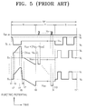
- FIG. 5 is a timing diagram of driving signals to be applied to the plasma display panel 1 illustrated in FIG. 1 in a single sub field SF of the subfields illustrated in FIG. 4.
- S AR1 , ..., ABm denote driving signals to be respectively applied to address electrode lines A R1 through A Bm of FIG. 1
- S X1 , ..., Xn denote driving signals to be respectively applied to the X electrode lines X 1 through X n of FIG.
- S Y1 through S Yn denote driving signals to be respectively applied to the Y electrode lines Y, through Y n of FIG. 1.
- FIG. 6 is a diagram illustrating the distribution of wall charges in a display cell at an instant of time t 5 of FIG. 5.
- FIG. 7 is a diagram illustrating the distribution of wall charges in a display cell at an instant of time t 8 of FIG. 5.
- the reference numerals that are the same as those of FIG. 2 denote the same elements. Referring to FIG. 5, in wall charge accumulation durations t1 through t5 of a reset period R of a sub field SF of FIG.
- an electric potential applied to Y electrode lines Y 1 through Y n is increased from a ground electric potential V G to a first electric potential V SET +
- having positive polarity e.g., 355 V, which is a maximum electric potential that is the addition of a sixth electric potential V SET and a third electric potential
- V SCL -V SCH having positive polarity is generated due to the difference between the second electric potential V SCL having negative polarity and the fourth electric potential V SCH having negative polarity.
- a ground electric potential V G is applied to X electrode lines X 1 through X n and address electrode lines A R1 through A Bm .
- discharge occurs among the Y electrode lines Y 1 through Y n and the X electrode lines X 1 through X n , and among the Y electrode lines Y 1 through Y n and the address electrode lines A R1 through A Bm .
- wall charges having negative polarity are formed around all the Y electrode lines Y 1 through Y n
- wall charges having positive polarity are formed around all the X electrode lines X 1 through X n
- wall charges having positive polarity are formed around all the address electrode lines A R1 through A Bm (see FIG. 6).
- an electric potential applied to the Y electrode lines Y 1 through Y n is reduced from the first electric potential V SET +
- a ground electric potential V G is applied to the address electrode lines A R1 through A Bm .
- discharge occurring among the X electrode lines X 1 through X n and the Y electrode lines Y 1 through Y n allows some of the wall charges formed around the Y electrode lines Y 1 through Y n to be appropriately moved around the X electrode lines X 1 through X n (see FIG. 8).
- the ground electric potential V G is applied to the address electrode lines A R1 through A Bm , and thus, the wall charges having positive polarity formed around the address electrode lines A R1 through A Bm are appropriately reduced (see FIG. 7).
- display-data signals S AR1, ..., ABm are applied to the address electrode lines A R1 through A Bm , and a scan pulse of the second electric potential V SCL having negative polarity is sequentially applied to the Y electrode lines Y 1 through Y n which are biased to the fourth electric potential V SCH having negative polarity, thereby smoothly performing addressing.
- the first address electric potential V A having positive polarity is applied when a display cell is selected, and the ground electric potential V G is applied otherwise.
- addressing discharge occurs in corresponding display cells, thus generating a wall potential equal to or higher than a set electric charge therein, but a wall potential equal to or higher than the set electric potential are not formed in the other display cells.
- the fifth electric potential V E1 having positive polarity is applied to the X electrode lines X 1 through X n in order that X electrode lines in selected display cells are influenced by the addressing discharge.
- sustain pulses of a seventh electric potential V S having positive polarity are alternately applied to all the Y electrode lines Y 1 through Y n and X electrode lines X 1 through X n . Therefore, in the sustain period S, sustain discharge occurs in the display cells in which the wall potential equal to or greater than the set electric potential was formed during the corresponding address period A A .
- a conventional discharge display apparatus as described above has a basic problem that comparatively loud noise is generated since it is driven by high ac voltage.
- a noise problem becomes serious, considering a recent trend that substrates of a discharge display apparatus (the front and rear glass substrates 10 and 13 of FIG. 1) become thinner and a driving voltage becomes higher due to partial pressure of discharge gas for high driving efficiency.
- the intensity of audible noise in a plasma display apparatus is significantly increased, when the thickness of the front glass substrate 10 of the plasma display panel 1 illustrated in FIG. 1 is less than 1.8 mm and the electric potential Vs, illustrated in FIG. 5, of the sustain pulses is greater than 200 V.
- the present invention provides a method of driving a discharge display panel while efficiently reducing audible noise generated in the discharge display apparatus.
- a method of driving a discharge display panel in which sub fields of a unit frame are given different gray-scale weights and are time-division driven, wherein at least one other sub field is present between a sub field given a maximum gray-scale weight and a sub field given a second largest gray-scale weight.
- noise generated in a discharge display apparatus has frequency characteristics that the intensity of audible noise in a most sensitive low-frequency band of human audible frequency bands diminishes when at least one sub field is present between a sub field given a maximum gray-scale weight and a sub field given a second largest gray-scale weight.
- FIG. 8 is a graph illustrating the audible noise characteristics of two models of plasma display apparatus taken over frequency. That is, in FIG. 8, reference numeral C81 denotes a plot showing the frequency characteristics of noise in a first model of plasma display apparatus, and reference numeral C81denotes a plot showing the frequency characteristics of noise in a second model of plasma display apparatus. Referring to FIG.
- the intensity of audible noise generated in a plasma display apparatus is increased of human audible frequency bands.
- the intensity of audible noise in the most sensitive low-frequency band of the human audible frequency bands must be reduced in order to efficiently reduce noise in the plasma display apparatus. For this, it is required to find out the factors that can change the frequency characteristics of noise in the plasma display apparatus.
- the thickness of the front glass substrate 10 of a plasma display panel is less than 1.8 mm and the electric potential V S of sustain pulses, such as those shown in FIG. 5, is greater than 200 V, the intensity of the above noise is significantly increased.
- FIG. 9 is a graph illustrating the frequency characteristics of driving signals applied to the plasma display panel 1 of FIG. 1 under various conditions when the method of FIG. 4 is performed.
- reference numeral C91 denotes a first frequency characteristic curve showing the frequency characteristics of driving signals obtained by performing Fourier transform on a combination of waveforms of driving signals when the plasma display panel 1 is driven according to the method of FIG. 4.
- the first frequency characteristics curve C91 shows that the levels of signal are comparatively high in a low-frequency band A9 which is a sensitive frequency band, as indicated by the frequency characteristics curves C81 and C82 of FIG. 8. That is, the frequency characteristics of noise vary depending on the frequency characteristics of the driving signals.
- Reference numeral C92 denotes a second frequency characteristic curve showing the frequency characteristics of driving signals obtained by performing Fourier transform on a combination of waveforms of driving signals when the plasma display panel 1 is driven according to the method of FIG. 4, using only the sustain periods S 1 through S 8 of the sub field SF 1 through SF 8 while removing the reset periods R 1 through R 8 and the address periods A 1 through A 8 thereof.
- the second frequency characteristic curve C92 is similar to the first frequency characteristic curve C91 in the low-frequency band A9 which is a sensitive frequency band. Accordingly, noise characteristics in the most sensitive low-frequency band A9 of the human audible frequency band are highly dependent on the sustain periods S 1 through S 8 .
- Reference numeral C93 denotes a third frequency characteristic curve showing the frequency characteristics of driving signals obtained by performing Fourier transform on a combination of waveforms of driving signals when the plasma display panel 1 is driven according to the method of FIG. 4, using only the seventh and eighth sustain periods S 7 and S 8 while removing the reset periods R 1 through R 8 , the address periods A 1 through A 8 , and the first through sixth sustain periods S 1 through S 6 of sub field SF 1 through SF 8 .
- the third frequency characteristic curve C93 is similar to the first and second frequency characteristic curves C91 and C92 in the low-frequency band A9 which is a sensitive frequency band.
- the noise characteristics of the most sensitive low-frequency band A9 of the human audible frequency bands are significantly dependent on the sustain periods S 1 through S 8, and particularly, sustain periods, such as the sustain periods S 7 and S 8 , which are given a high gray-scale weight.
- the noise characteristics of the most sensitive low-frequency band A9 of the human audible frequency bands are significantly dependent on time intervals (time intervals R 8 and A 8 ) between sustain periods (the sustain periods S 7 and S 8 ), which are given a high gray-scale weight, and the durations of the sustain periods (durations 64T and 128T).
- time intervals R 8 and A 8 time intervals between sustain periods (the sustain periods S 7 and S 8 ), which are given a high gray-scale weight
- the durations of the sustain periods durations 64T and 128T.
- FIG. 10 is a graph illustrating the frequency characteristics C101 of driving signals applied to the plasma display panel 1 of FIG. 1 and the frequency characteristics C102 of resultant noise when using the structure of sub fields to which gray-scale weights are allocated in ascending order as in the conventional method of FIG. 4.
- FIG. 11 is a graph illustrating the frequency characteristics of driving signals applied to the plasma display panel of FIG. 1 by using only the three sub fields, of the subfields illustrated in FIG. 4, to which first through third largest gray-scale weights are allocated, and the frequency characteristics of resultant noise.
- FIG. 12 is a graph illustrating the frequency characteristics of driving signals applied to the plasma display panel 1 of FIG. 1, when using the structure of subfields in which another sub field is present between a sub field given a maximum gray-scale weight and a sub field given a second largest gray-scale weight and between the sub field given the second largest gray-scale weight and a sub field given a third largest gray-scale weight, and the frequency characteristics of resultant noise.
- FIG. 13 is a graph illustrating the frequency characteristics of driving signals applied to the plasma display panel 1 of FIG. 1, when using the structure of subfields in which two other sub fields are present between a sub field given a maximum gray-scale weight and a sub field given a second largest gray-scale weight and between the sub field given the second largest gray-scale weight and a sub field given a third largest gray-scale weight, and the frequency characteristics of resultant noise.
- Table 1 shows gray-scale weights allocated to 11 sub fields SF 1 through SF 11 used to obtain the frequency characteristics curves illustrated in FIGS. 10 through 13. [Table 1] SF 1 SF 2 SF 3 SF 4 SF 5 SF 6 SF 7 SF 8 SF 9 SF 10 SF 11 FIG.
- FIGS. 10 and 11 A comparison of FIGS. 10 and 11 reveals that the frequency characteristics C101 and C111 of driving signals are similar in most sensitive low-frequency bands A10 and A11 of human audible frequency bands, and thus, the frequency characteristics C102 and C112 of noise are also similar to each other. That is, the noise characteristics in the most sensitive low-frequency bands A10 and A11 are significantly dependent on the sub fields SF 9 through SF 11 allocated high gray-scale weights sustain periods.
- FIGS. 10 and 12 a comparison of FIGS. 10 and 12 reveals that the frequency characteristics C101 and C121 of driving signals are different from each other, and thus, the frequency characteristics C102 and C122 of noise are also different from each other. More specifically, the intensity of audible noise illustrated in FIG. 12 is lower than that of noise illustrated in FIG. 10 in the most sensitive low-frequency bands A10 and A121 of human audible frequency bands. Thus, FIG.
- FIGS. 10 and 13 a comparison of FIGS. 10 and 13 reveals that the frequency characteristics C101 and C131 of driving signals are different from each other, and thus, the frequency characteristics C102 and C132 of audible noise are also different from each other. More specifically, the intensity of audible noise illustrated in FIG. 13 is lower than that of audible noise illustrated in FIG. 10 in the most sensitive low-frequency bands A10 and A131 of the human audible frequency bands. Thus, FIG.
- FIG. 14 is a timing diagram illustrating a method of driving a discharge display panel based on the experiment results illustrated in FIGS. 8 through 13, according to an embodiment of the present invention.
- each of all unit frames is divided into 8 sub fields SF 1 through SF 8 .
- the sub fields SF 1 through SF 8 are divided into reset periods R 1 through R 8 , address periods A 1 through A 8 , and sustain periods S 1 through S 8 .
- FIG. 15 is a timing diagram illustrating a method of driving a discharge display panel based on the experiment results illustrated in FIGS. 8 through 13, according to another embodiment of the present invention. Referring to FIG.
- each of all unit frames is divided into 8 sub fields SF 1 through SF 8 .
- the sub fields SF 1 through SF 8 are divided into reset periods R 1 through R 8, address periods A 1 through A 8, and sustain periods S 1 through S 8 .
- the two sub fields SF 2 and SF 3 are present between the sub field SF 1 given a maximum gray-scale weight and the sub field SF 4 given a second largest gray-scale weight.
- the sub field SF 5 is present between the sub field SF 4 given the second largest gray-scale weight and the sub field SF 6 given a third largest gray-scale weight. Accordingly, it is possible to efficiently reduce audible noise in a plasma display apparatus, as described above with reference to Table 1 and FIGS. 10 through 13. As described above, according to a method of driving a discharge display panel according to the present invention, noise in a discharge display apparatus can be efficiently reduced.
Landscapes
- Engineering & Computer Science (AREA)
- Physics & Mathematics (AREA)
- Computer Hardware Design (AREA)
- General Physics & Mathematics (AREA)
- Theoretical Computer Science (AREA)
- Power Engineering (AREA)
- Plasma & Fusion (AREA)
- Control Of Indicators Other Than Cathode Ray Tubes (AREA)
- Control Of Gas Discharge Display Tubes (AREA)
Applications Claiming Priority (1)
| Application Number | Priority Date | Filing Date | Title |
|---|---|---|---|
| KR1020060089248A KR100911006B1 (ko) | 2006-09-14 | 2006-09-14 | 소음을 줄이기 위한 방전 디스플레이 패널의 구동 방법 |
Publications (2)
| Publication Number | Publication Date |
|---|---|
| EP1901267A2 true EP1901267A2 (de) | 2008-03-19 |
| EP1901267A3 EP1901267A3 (de) | 2009-12-02 |
Family
ID=38828365
Family Applications (1)
| Application Number | Title | Priority Date | Filing Date |
|---|---|---|---|
| EP07115759A Withdrawn EP1901267A3 (de) | 2006-09-14 | 2007-09-05 | Verfahren zur Ansteuerung einer Entladungsanzeigetafel zur Reduktion von hörbarem Geräusch |
Country Status (3)
| Country | Link |
|---|---|
| EP (1) | EP1901267A3 (de) |
| KR (1) | KR100911006B1 (de) |
| CN (1) | CN101145312A (de) |
Cited By (2)
| Publication number | Priority date | Publication date | Assignee | Title |
|---|---|---|---|---|
| US9172735B2 (en) | 2000-01-28 | 2015-10-27 | Comcast Ip Holdings I, Llc | Method and apparatus for content distribution via non-homogeneous access networks |
| US12592176B2 (en) | 2021-05-03 | 2026-03-31 | Samsung Electronics Co., Ltd. | Electronic apparatus and control method thereof for providing a progressive or interlaced scanning method |
Family Cites Families (8)
| Publication number | Priority date | Publication date | Assignee | Title |
|---|---|---|---|---|
| WO1998039762A1 (en) * | 1997-03-07 | 1998-09-11 | Koninklijke Philips Electronics N.V. | A circuit for and method of driving a flat panel display in a sub field mode and a flat panel display with such a circuit |
| KR20010087485A (ko) * | 2000-03-07 | 2001-09-21 | 김순택 | 플라즈마 표시패널의 구동방법 |
| EP1326223A1 (de) * | 2000-11-30 | 2003-07-09 | THOMSON multimedia S.A. | Verfahren und Vorrichtung zur Steuerung eines Anzeigegeräts |
| KR100508238B1 (ko) * | 2002-12-26 | 2005-08-17 | 엘지전자 주식회사 | 휴지기간을 가지는 플라즈마 디스플레이 패널의 구동방법 |
| JP4385121B2 (ja) * | 2003-09-22 | 2009-12-16 | パナソニック株式会社 | 表示装置 |
| JP2005258140A (ja) * | 2004-03-12 | 2005-09-22 | Matsushita Electric Ind Co Ltd | 画像表示方法 |
| KR20050112834A (ko) * | 2004-05-28 | 2005-12-01 | 삼성에스디아이 주식회사 | 플라즈마 표시 장치 및 그의 구동 방법 |
| JP4867170B2 (ja) * | 2005-01-17 | 2012-02-01 | パナソニック株式会社 | 画像表示方法 |
-
2006
- 2006-09-14 KR KR1020060089248A patent/KR100911006B1/ko not_active Expired - Fee Related
-
2007
- 2007-09-05 EP EP07115759A patent/EP1901267A3/de not_active Withdrawn
- 2007-09-14 CN CNA2007101537339A patent/CN101145312A/zh active Pending
Cited By (4)
| Publication number | Priority date | Publication date | Assignee | Title |
|---|---|---|---|---|
| US9172735B2 (en) | 2000-01-28 | 2015-10-27 | Comcast Ip Holdings I, Llc | Method and apparatus for content distribution via non-homogeneous access networks |
| US9596284B2 (en) | 2000-01-28 | 2017-03-14 | Comcast Ip Holdings I, Llc | Content distribution via a distribution network and an access network |
| US10257246B2 (en) | 2000-01-28 | 2019-04-09 | Comcast Ip Holdings I, Llc | Content distribution via a distribution network and an access network |
| US12592176B2 (en) | 2021-05-03 | 2026-03-31 | Samsung Electronics Co., Ltd. | Electronic apparatus and control method thereof for providing a progressive or interlaced scanning method |
Also Published As
| Publication number | Publication date |
|---|---|
| EP1901267A3 (de) | 2009-12-02 |
| CN101145312A (zh) | 2008-03-19 |
| KR100911006B1 (ko) | 2009-08-05 |
| KR20080024747A (ko) | 2008-03-19 |
Similar Documents
| Publication | Publication Date | Title |
|---|---|---|
| US6744218B2 (en) | Method of driving a plasma display panel in which the width of display sustain pulse varies | |
| JP4068089B2 (ja) | アドレス−ディスプレイ混合による放電ディスプレイパネルの駆動方法 | |
| JP2005122148A (ja) | パネル駆動方法、パネル駆動装置及びディスプレイパネル | |
| JP5000983B2 (ja) | プラズマディスプレイ装置 | |
| KR100911006B1 (ko) | 소음을 줄이기 위한 방전 디스플레이 패널의 구동 방법 | |
| KR100573124B1 (ko) | 플라즈마 디스플레이 패널 구동방법 및 장치 | |
| KR20050080233A (ko) | 패널구동방법 | |
| JP2001042820A (ja) | プラズマディスプレイパネルの駆動方法及びその駆動装置 | |
| KR100719565B1 (ko) | 저계조 디스플레이의 선형성이 증진되는 방전 디스플레이패널의 구동 방법 | |
| KR100777726B1 (ko) | 효과적인 초기화가 수행되는 방전 디스플레이 패널의 구동방법 | |
| KR100581877B1 (ko) | 플라즈마 디스플레이 패널 구동방법 | |
| JP4208859B2 (ja) | 外圧によって輝度が調整される放電ディスプレイ装置 | |
| KR100424264B1 (ko) | 초기 상태의 개선을 위한 플라즈마 디스플레이 패널의구동 방법 | |
| KR100573113B1 (ko) | 효율적인 리셋팅이 수행되는 플라즈마 디스플레이 패널의구동 방법 | |
| KR100537610B1 (ko) | 디스플레이-유지 펄스들의 주파수가 변하는 플라즈마디스플레이 패널의 구동 방법 | |
| KR100751335B1 (ko) | 플라즈마 디스플레이 패널 구동방법 | |
| KR20070094093A (ko) | 유지 펄스가 전기적인 플로팅의 영역을 포함하는 방전디스플레이 패널의 구동 방법 | |
| KR20050106550A (ko) | 효율적인 리셋팅이 수행되는 방전 디스플레이 패널의 구동방법 | |
| US20070109221A1 (en) | Method of driving discharge display panel for effective initialization | |
| KR20060027510A (ko) | 효율적인 리셋팅이 수행되는 방전 디스플레이 장치 | |
| KR20050052645A (ko) | 플라즈마 디스플레이 패널 구동방법 | |
| KR20080038543A (ko) | 유지 펄스들의 주파수가 변하는 방전 디스플레이 패널의구동 방법 | |
| JP2012225965A (ja) | プラズマディスプレイ装置およびプラズマディスプレイパネルの駆動方法 | |
| KR20080006887A (ko) | 디스플레이-데이터 펄스들의 전위가 변하는 방전디스플레이 패널의 구동 방법 | |
| KR20050041170A (ko) | 패널구동방법 |
Legal Events
| Date | Code | Title | Description |
|---|---|---|---|
| PUAI | Public reference made under article 153(3) epc to a published international application that has entered the european phase |
Free format text: ORIGINAL CODE: 0009012 |
|
| 17P | Request for examination filed |
Effective date: 20070905 |
|
| AK | Designated contracting states |
Kind code of ref document: A2 Designated state(s): AT BE BG CH CY CZ DE DK EE ES FI FR GB GR HU IE IS IT LI LT LU LV MC MT NL PL PT RO SE SI SK TR |
|
| AX | Request for extension of the european patent |
Extension state: AL BA HR MK YU |
|
| RAP1 | Party data changed (applicant data changed or rights of an application transferred) |
Owner name: SAMSUNG SDI CO., LTD. |
|
| PUAL | Search report despatched |
Free format text: ORIGINAL CODE: 0009013 |
|
| AK | Designated contracting states |
Kind code of ref document: A3 Designated state(s): AT BE BG CH CY CZ DE DK EE ES FI FR GB GR HU IE IS IT LI LT LU LV MC MT NL PL PT RO SE SI SK TR |
|
| AX | Request for extension of the european patent |
Extension state: AL BA HR MK RS |
|
| AKX | Designation fees paid |
Designated state(s): DE FR GB HU |
|
| STAA | Information on the status of an ep patent application or granted ep patent |
Free format text: STATUS: THE APPLICATION IS DEEMED TO BE WITHDRAWN |
|
| 18D | Application deemed to be withdrawn |
Effective date: 20100604 |