EP1898455A1 - Interlayer insulating film and wiring structure, and process for producing the same - Google Patents
Interlayer insulating film and wiring structure, and process for producing the same Download PDFInfo
- Publication number
- EP1898455A1 EP1898455A1 EP06766953A EP06766953A EP1898455A1 EP 1898455 A1 EP1898455 A1 EP 1898455A1 EP 06766953 A EP06766953 A EP 06766953A EP 06766953 A EP06766953 A EP 06766953A EP 1898455 A1 EP1898455 A1 EP 1898455A1
- Authority
- EP
- European Patent Office
- Prior art keywords
- film
- fluorocarbon
- gas
- fluorocarbon film
- layer
- Prior art date
- Legal status (The legal status is an assumption and is not a legal conclusion. Google has not performed a legal analysis and makes no representation as to the accuracy of the status listed.)
- Granted
Links
- 239000011229 interlayer Substances 0.000 title claims abstract description 68
- 238000000034 method Methods 0.000 title claims description 61
- 230000008569 process Effects 0.000 title description 14
- NBVXSUQYWXRMNV-UHFFFAOYSA-N fluoromethane Chemical compound FC NBVXSUQYWXRMNV-UHFFFAOYSA-N 0.000 claims abstract description 145
- 239000010410 layer Substances 0.000 claims abstract description 106
- 239000000758 substrate Substances 0.000 claims abstract description 20
- 239000002184 metal Substances 0.000 claims abstract description 19
- 229910052751 metal Inorganic materials 0.000 claims abstract description 19
- ABTOQLMXBSRXSM-UHFFFAOYSA-N silicon tetrafluoride Chemical compound F[Si](F)(F)F ABTOQLMXBSRXSM-UHFFFAOYSA-N 0.000 claims abstract description 17
- 239000007789 gas Substances 0.000 claims description 150
- 238000000137 annealing Methods 0.000 claims description 69
- VYPSYNLAJGMNEJ-UHFFFAOYSA-N Silicium dioxide Chemical compound O=[Si]=O VYPSYNLAJGMNEJ-UHFFFAOYSA-N 0.000 claims description 57
- PXHVJJICTQNCMI-UHFFFAOYSA-N Nickel Chemical compound [Ni] PXHVJJICTQNCMI-UHFFFAOYSA-N 0.000 claims description 38
- 230000004888 barrier function Effects 0.000 claims description 33
- 238000005121 nitriding Methods 0.000 claims description 32
- 239000010949 copper Substances 0.000 claims description 27
- 238000004519 manufacturing process Methods 0.000 claims description 21
- DBJLJFTWODWSOF-UHFFFAOYSA-L nickel(ii) fluoride Chemical compound F[Ni]F DBJLJFTWODWSOF-UHFFFAOYSA-L 0.000 claims description 21
- 229910052581 Si3N4 Inorganic materials 0.000 claims description 20
- 229910052759 nickel Inorganic materials 0.000 claims description 16
- 238000009792 diffusion process Methods 0.000 claims description 14
- 239000012298 atmosphere Substances 0.000 claims description 12
- 229910052802 copper Inorganic materials 0.000 claims description 12
- KRHYYFGTRYWZRS-UHFFFAOYSA-M Fluoride anion Chemical compound [F-] KRHYYFGTRYWZRS-UHFFFAOYSA-M 0.000 claims description 10
- BLRPTPMANUNPDV-UHFFFAOYSA-N Silane Chemical compound [SiH4] BLRPTPMANUNPDV-UHFFFAOYSA-N 0.000 claims description 10
- RYGMFSIKBFXOCR-UHFFFAOYSA-N Copper Chemical compound [Cu] RYGMFSIKBFXOCR-UHFFFAOYSA-N 0.000 claims description 9
- 229910052743 krypton Inorganic materials 0.000 claims description 9
- 229910052724 xenon Inorganic materials 0.000 claims description 9
- 238000006243 chemical reaction Methods 0.000 claims description 8
- 238000004140 cleaning Methods 0.000 claims description 6
- 238000011049 filling Methods 0.000 claims description 5
- 230000001590 oxidative effect Effects 0.000 claims description 5
- 239000001301 oxygen Substances 0.000 claims description 5
- 229910052760 oxygen Inorganic materials 0.000 claims description 5
- UFHFLCQGNIYNRP-UHFFFAOYSA-N Hydrogen Chemical compound [H][H] UFHFLCQGNIYNRP-UHFFFAOYSA-N 0.000 claims description 4
- QVGXLLKOCUKJST-UHFFFAOYSA-N atomic oxygen Chemical compound [O] QVGXLLKOCUKJST-UHFFFAOYSA-N 0.000 claims description 4
- 239000004020 conductor Substances 0.000 claims description 4
- 239000001257 hydrogen Substances 0.000 claims description 4
- 229910052739 hydrogen Inorganic materials 0.000 claims description 4
- 239000011261 inert gas Substances 0.000 claims description 4
- 239000000463 material Substances 0.000 claims description 4
- 238000005240 physical vapour deposition Methods 0.000 claims description 4
- 230000001678 irradiating effect Effects 0.000 claims description 3
- 238000002488 metal-organic chemical vapour deposition Methods 0.000 claims description 3
- IJGRMHOSHXDMSA-UHFFFAOYSA-N Atomic nitrogen Chemical compound N#N IJGRMHOSHXDMSA-UHFFFAOYSA-N 0.000 claims description 2
- 229910001873 dinitrogen Inorganic materials 0.000 claims description 2
- XPBBUZJBQWWFFJ-UHFFFAOYSA-N fluorosilane Chemical compound [SiH3]F XPBBUZJBQWWFFJ-UHFFFAOYSA-N 0.000 claims description 2
- 229910052681 coesite Inorganic materials 0.000 claims 6
- 229910052906 cristobalite Inorganic materials 0.000 claims 6
- 239000000377 silicon dioxide Substances 0.000 claims 6
- 229910052682 stishovite Inorganic materials 0.000 claims 6
- 229910052905 tridymite Inorganic materials 0.000 claims 6
- 239000004065 semiconductor Substances 0.000 abstract description 20
- 229910004014 SiF4 Inorganic materials 0.000 abstract 1
- 238000010586 diagram Methods 0.000 description 61
- 229910052814 silicon oxide Inorganic materials 0.000 description 45
- 238000010943 off-gassing Methods 0.000 description 35
- 230000015572 biosynthetic process Effects 0.000 description 21
- 238000009832 plasma treatment Methods 0.000 description 18
- 229910021587 Nickel(II) fluoride Inorganic materials 0.000 description 17
- XLYOFNOQVPJJNP-UHFFFAOYSA-N water Substances O XLYOFNOQVPJJNP-UHFFFAOYSA-N 0.000 description 16
- HQVNEWCFYHHQES-UHFFFAOYSA-N silicon nitride Chemical compound N12[Si]34N5[Si]62N3[Si]51N64 HQVNEWCFYHHQES-UHFFFAOYSA-N 0.000 description 14
- 230000000694 effects Effects 0.000 description 12
- 238000010438 heat treatment Methods 0.000 description 10
- 238000005259 measurement Methods 0.000 description 9
- XUIMIQQOPSSXEZ-UHFFFAOYSA-N Silicon Chemical compound [Si] XUIMIQQOPSSXEZ-UHFFFAOYSA-N 0.000 description 7
- 239000012790 adhesive layer Substances 0.000 description 7
- 229910052799 carbon Inorganic materials 0.000 description 7
- 238000011065 in-situ storage Methods 0.000 description 7
- 229910052710 silicon Inorganic materials 0.000 description 7
- 239000010703 silicon Substances 0.000 description 7
- 238000001228 spectrum Methods 0.000 description 7
- 238000012545 processing Methods 0.000 description 6
- 238000000354 decomposition reaction Methods 0.000 description 5
- 238000012360 testing method Methods 0.000 description 5
- -1 SiCN Chemical compound 0.000 description 4
- 238000004833 X-ray photoelectron spectroscopy Methods 0.000 description 4
- 238000005530 etching Methods 0.000 description 4
- 230000006872 improvement Effects 0.000 description 3
- 239000012212 insulator Substances 0.000 description 3
- 238000011835 investigation Methods 0.000 description 3
- XKRFYHLGVUSROY-UHFFFAOYSA-N Argon Chemical compound [Ar] XKRFYHLGVUSROY-UHFFFAOYSA-N 0.000 description 2
- OKTJSMMVPCPJKN-UHFFFAOYSA-N Carbon Chemical compound [C] OKTJSMMVPCPJKN-UHFFFAOYSA-N 0.000 description 2
- 229910004016 SiF2 Inorganic materials 0.000 description 2
- 229910052786 argon Inorganic materials 0.000 description 2
- 230000007423 decrease Effects 0.000 description 2
- 238000003795 desorption Methods 0.000 description 2
- MGNHOGAVECORPT-UHFFFAOYSA-N difluorosilicon Chemical compound F[Si]F MGNHOGAVECORPT-UHFFFAOYSA-N 0.000 description 2
- 238000010790 dilution Methods 0.000 description 2
- 239000012895 dilution Substances 0.000 description 2
- 238000006073 displacement reaction Methods 0.000 description 2
- 238000000921 elemental analysis Methods 0.000 description 2
- 238000011156 evaluation Methods 0.000 description 2
- 239000000203 mixture Substances 0.000 description 2
- 150000004767 nitrides Chemical class 0.000 description 2
- 230000003071 parasitic effect Effects 0.000 description 2
- 229910000077 silane Inorganic materials 0.000 description 2
- 230000003595 spectral effect Effects 0.000 description 2
- 238000004611 spectroscopical analysis Methods 0.000 description 2
- TXEYQDLBPFQVAA-UHFFFAOYSA-N tetrafluoromethane Chemical compound FC(F)(F)F TXEYQDLBPFQVAA-UHFFFAOYSA-N 0.000 description 2
- 230000036962 time dependent Effects 0.000 description 2
- ATVLVRVBCRICNU-UHFFFAOYSA-N trifluorosilicon Chemical compound F[Si](F)F ATVLVRVBCRICNU-UHFFFAOYSA-N 0.000 description 2
- YBMDPYAEZDJWNY-UHFFFAOYSA-N 1,2,3,3,4,4,5,5-octafluorocyclopentene Chemical compound FC1=C(F)C(F)(F)C(F)(F)C1(F)F YBMDPYAEZDJWNY-UHFFFAOYSA-N 0.000 description 1
- RLMMCBZQTSRCHJ-UHFFFAOYSA-N 1-fluorocyclobutene Chemical compound FC1=CCC1 RLMMCBZQTSRCHJ-UHFFFAOYSA-N 0.000 description 1
- BKGFFXQUCIPKJK-UHFFFAOYSA-N 1-fluorocyclopropene Chemical compound FC1=CC1 BKGFFXQUCIPKJK-UHFFFAOYSA-N 0.000 description 1
- 239000004215 Carbon black (E152) Substances 0.000 description 1
- MYMOFIZGZYHOMD-UHFFFAOYSA-N Dioxygen Chemical compound O=O MYMOFIZGZYHOMD-UHFFFAOYSA-N 0.000 description 1
- VGGSQFUCUMXWEO-UHFFFAOYSA-N Ethene Chemical compound C=C VGGSQFUCUMXWEO-UHFFFAOYSA-N 0.000 description 1
- 239000005977 Ethylene Substances 0.000 description 1
- 230000009471 action Effects 0.000 description 1
- 125000001931 aliphatic group Chemical group 0.000 description 1
- 239000012159 carrier gas Substances 0.000 description 1
- 230000008859 change Effects 0.000 description 1
- 238000011109 contamination Methods 0.000 description 1
- 229910001882 dioxygen Inorganic materials 0.000 description 1
- 238000002474 experimental method Methods 0.000 description 1
- 150000002222 fluorine compounds Chemical class 0.000 description 1
- SKRPCQXQBBHPKO-UHFFFAOYSA-N fluorocyclobutane Chemical compound FC1CCC1 SKRPCQXQBBHPKO-UHFFFAOYSA-N 0.000 description 1
- IZZJFOLOOYFYFG-VKHMYHEASA-N fluorocyclopropane Chemical compound F[C@H]1[CH]C1 IZZJFOLOOYFYFG-VKHMYHEASA-N 0.000 description 1
- 229930195733 hydrocarbon Natural products 0.000 description 1
- 150000002430 hydrocarbons Chemical class 0.000 description 1
- 238000009413 insulation Methods 0.000 description 1
- 238000010406 interfacial reaction Methods 0.000 description 1
- DNNSSWSSYDEUBZ-UHFFFAOYSA-N krypton atom Chemical compound [Kr] DNNSSWSSYDEUBZ-UHFFFAOYSA-N 0.000 description 1
- 239000012299 nitrogen atmosphere Substances 0.000 description 1
- 125000004433 nitrogen atom Chemical group N* 0.000 description 1
- 150000002831 nitrogen free-radicals Chemical class 0.000 description 1
- 230000003647 oxidation Effects 0.000 description 1
- 238000007254 oxidation reaction Methods 0.000 description 1
- 238000005268 plasma chemical vapour deposition Methods 0.000 description 1
- HBMJWWWQQXIZIP-UHFFFAOYSA-N silicon carbide Chemical compound [Si+]#[C-] HBMJWWWQQXIZIP-UHFFFAOYSA-N 0.000 description 1
- 150000003377 silicon compounds Chemical class 0.000 description 1
- 230000003746 surface roughness Effects 0.000 description 1
- FHNFHKCVQCLJFQ-UHFFFAOYSA-N xenon atom Chemical compound [Xe] FHNFHKCVQCLJFQ-UHFFFAOYSA-N 0.000 description 1
Images


Classifications
-
- H—ELECTRICITY
- H01—ELECTRIC ELEMENTS
- H01L—SEMICONDUCTOR DEVICES NOT COVERED BY CLASS H10
- H01L23/00—Details of semiconductor or other solid state devices
- H01L23/48—Arrangements for conducting electric current to or from the solid state body in operation, e.g. leads, terminal arrangements ; Selection of materials therefor
- H01L23/488—Arrangements for conducting electric current to or from the solid state body in operation, e.g. leads, terminal arrangements ; Selection of materials therefor consisting of soldered or bonded constructions
- H01L23/498—Leads, i.e. metallisations or lead-frames on insulating substrates, e.g. chip carriers
- H01L23/49866—Leads, i.e. metallisations or lead-frames on insulating substrates, e.g. chip carriers characterised by the materials
- H01L23/49894—Materials of the insulating layers or coatings
-
- H—ELECTRICITY
- H01—ELECTRIC ELEMENTS
- H01L—SEMICONDUCTOR DEVICES NOT COVERED BY CLASS H10
- H01L21/00—Processes or apparatus adapted for the manufacture or treatment of semiconductor or solid state devices or of parts thereof
- H01L21/02—Manufacture or treatment of semiconductor devices or of parts thereof
- H01L21/02104—Forming layers
- H01L21/02107—Forming insulating materials on a substrate
- H01L21/02109—Forming insulating materials on a substrate characterised by the type of layer, e.g. type of material, porous/non-porous, pre-cursors, mixtures or laminates
- H01L21/02112—Forming insulating materials on a substrate characterised by the type of layer, e.g. type of material, porous/non-porous, pre-cursors, mixtures or laminates characterised by the material of the layer
- H01L21/02118—Forming insulating materials on a substrate characterised by the type of layer, e.g. type of material, porous/non-porous, pre-cursors, mixtures or laminates characterised by the material of the layer carbon based polymeric organic or inorganic material, e.g. polyimides, poly cyclobutene or PVC
- H01L21/0212—Forming insulating materials on a substrate characterised by the type of layer, e.g. type of material, porous/non-porous, pre-cursors, mixtures or laminates characterised by the material of the layer carbon based polymeric organic or inorganic material, e.g. polyimides, poly cyclobutene or PVC the material being fluoro carbon compounds, e.g.(CFx) n, (CHxFy) n or polytetrafluoroethylene
-
- H—ELECTRICITY
- H01—ELECTRIC ELEMENTS
- H01L—SEMICONDUCTOR DEVICES NOT COVERED BY CLASS H10
- H01L21/00—Processes or apparatus adapted for the manufacture or treatment of semiconductor or solid state devices or of parts thereof
- H01L21/02—Manufacture or treatment of semiconductor devices or of parts thereof
- H01L21/02104—Forming layers
- H01L21/02107—Forming insulating materials on a substrate
- H01L21/02225—Forming insulating materials on a substrate characterised by the process for the formation of the insulating layer
- H01L21/0226—Forming insulating materials on a substrate characterised by the process for the formation of the insulating layer formation by a deposition process
- H01L21/02263—Forming insulating materials on a substrate characterised by the process for the formation of the insulating layer formation by a deposition process deposition from the gas or vapour phase
- H01L21/02271—Forming insulating materials on a substrate characterised by the process for the formation of the insulating layer formation by a deposition process deposition from the gas or vapour phase deposition by decomposition or reaction of gaseous or vapour phase compounds, i.e. chemical vapour deposition
- H01L21/02274—Forming insulating materials on a substrate characterised by the process for the formation of the insulating layer formation by a deposition process deposition from the gas or vapour phase deposition by decomposition or reaction of gaseous or vapour phase compounds, i.e. chemical vapour deposition in the presence of a plasma [PECVD]
-
- H—ELECTRICITY
- H01—ELECTRIC ELEMENTS
- H01L—SEMICONDUCTOR DEVICES NOT COVERED BY CLASS H10
- H01L21/00—Processes or apparatus adapted for the manufacture or treatment of semiconductor or solid state devices or of parts thereof
- H01L21/02—Manufacture or treatment of semiconductor devices or of parts thereof
- H01L21/02104—Forming layers
- H01L21/02107—Forming insulating materials on a substrate
- H01L21/02296—Forming insulating materials on a substrate characterised by the treatment performed before or after the formation of the layer
- H01L21/02318—Forming insulating materials on a substrate characterised by the treatment performed before or after the formation of the layer post-treatment
- H01L21/02321—Forming insulating materials on a substrate characterised by the treatment performed before or after the formation of the layer post-treatment introduction of substances into an already existing insulating layer
- H01L21/02329—Forming insulating materials on a substrate characterised by the treatment performed before or after the formation of the layer post-treatment introduction of substances into an already existing insulating layer introduction of nitrogen
-
- H—ELECTRICITY
- H01—ELECTRIC ELEMENTS
- H01L—SEMICONDUCTOR DEVICES NOT COVERED BY CLASS H10
- H01L21/00—Processes or apparatus adapted for the manufacture or treatment of semiconductor or solid state devices or of parts thereof
- H01L21/02—Manufacture or treatment of semiconductor devices or of parts thereof
- H01L21/02104—Forming layers
- H01L21/02107—Forming insulating materials on a substrate
- H01L21/02296—Forming insulating materials on a substrate characterised by the treatment performed before or after the formation of the layer
- H01L21/02318—Forming insulating materials on a substrate characterised by the treatment performed before or after the formation of the layer post-treatment
- H01L21/02337—Forming insulating materials on a substrate characterised by the treatment performed before or after the formation of the layer post-treatment treatment by exposure to a gas or vapour
- H01L21/0234—Forming insulating materials on a substrate characterised by the treatment performed before or after the formation of the layer post-treatment treatment by exposure to a gas or vapour treatment by exposure to a plasma
-
- H—ELECTRICITY
- H01—ELECTRIC ELEMENTS
- H01L—SEMICONDUCTOR DEVICES NOT COVERED BY CLASS H10
- H01L21/00—Processes or apparatus adapted for the manufacture or treatment of semiconductor or solid state devices or of parts thereof
- H01L21/02—Manufacture or treatment of semiconductor devices or of parts thereof
- H01L21/02104—Forming layers
- H01L21/02107—Forming insulating materials on a substrate
- H01L21/02296—Forming insulating materials on a substrate characterised by the treatment performed before or after the formation of the layer
- H01L21/02318—Forming insulating materials on a substrate characterised by the treatment performed before or after the formation of the layer post-treatment
- H01L21/02362—Forming insulating materials on a substrate characterised by the treatment performed before or after the formation of the layer post-treatment formation of intermediate layers, e.g. capping layers or diffusion barriers
-
- H—ELECTRICITY
- H01—ELECTRIC ELEMENTS
- H01L—SEMICONDUCTOR DEVICES NOT COVERED BY CLASS H10
- H01L21/00—Processes or apparatus adapted for the manufacture or treatment of semiconductor or solid state devices or of parts thereof
- H01L21/02—Manufacture or treatment of semiconductor devices or of parts thereof
- H01L21/04—Manufacture or treatment of semiconductor devices or of parts thereof the devices having potential barriers, e.g. a PN junction, depletion layer or carrier concentration layer
- H01L21/18—Manufacture or treatment of semiconductor devices or of parts thereof the devices having potential barriers, e.g. a PN junction, depletion layer or carrier concentration layer the devices having semiconductor bodies comprising elements of Group IV of the Periodic Table or AIIIBV compounds with or without impurities, e.g. doping materials
- H01L21/30—Treatment of semiconductor bodies using processes or apparatus not provided for in groups H01L21/20 - H01L21/26
- H01L21/31—Treatment of semiconductor bodies using processes or apparatus not provided for in groups H01L21/20 - H01L21/26 to form insulating layers thereon, e.g. for masking or by using photolithographic techniques; After treatment of these layers; Selection of materials for these layers
- H01L21/312—Organic layers, e.g. photoresist
- H01L21/3127—Layers comprising fluoro (hydro)carbon compounds, e.g. polytetrafluoroethylene
-
- H—ELECTRICITY
- H01—ELECTRIC ELEMENTS
- H01L—SEMICONDUCTOR DEVICES NOT COVERED BY CLASS H10
- H01L21/00—Processes or apparatus adapted for the manufacture or treatment of semiconductor or solid state devices or of parts thereof
- H01L21/70—Manufacture or treatment of devices consisting of a plurality of solid state components formed in or on a common substrate or of parts thereof; Manufacture of integrated circuit devices or of parts thereof
- H01L21/71—Manufacture of specific parts of devices defined in group H01L21/70
- H01L21/768—Applying interconnections to be used for carrying current between separate components within a device comprising conductors and dielectrics
- H01L21/76801—Applying interconnections to be used for carrying current between separate components within a device comprising conductors and dielectrics characterised by the formation and the after-treatment of the dielectrics, e.g. smoothing
- H01L21/76835—Combinations of two or more different dielectric layers having a low dielectric constant
-
- H—ELECTRICITY
- H01—ELECTRIC ELEMENTS
- H01L—SEMICONDUCTOR DEVICES NOT COVERED BY CLASS H10
- H01L23/00—Details of semiconductor or other solid state devices
- H01L23/52—Arrangements for conducting electric current within the device in operation from one component to another, i.e. interconnections, e.g. wires, lead frames
- H01L23/522—Arrangements for conducting electric current within the device in operation from one component to another, i.e. interconnections, e.g. wires, lead frames including external interconnections consisting of a multilayer structure of conductive and insulating layers inseparably formed on the semiconductor body
- H01L23/532—Arrangements for conducting electric current within the device in operation from one component to another, i.e. interconnections, e.g. wires, lead frames including external interconnections consisting of a multilayer structure of conductive and insulating layers inseparably formed on the semiconductor body characterised by the materials
- H01L23/5329—Insulating materials
- H01L23/53295—Stacked insulating layers
-
- H—ELECTRICITY
- H01—ELECTRIC ELEMENTS
- H01L—SEMICONDUCTOR DEVICES NOT COVERED BY CLASS H10
- H01L21/00—Processes or apparatus adapted for the manufacture or treatment of semiconductor or solid state devices or of parts thereof
- H01L21/02—Manufacture or treatment of semiconductor devices or of parts thereof
- H01L21/02104—Forming layers
- H01L21/02107—Forming insulating materials on a substrate
- H01L21/02109—Forming insulating materials on a substrate characterised by the type of layer, e.g. type of material, porous/non-porous, pre-cursors, mixtures or laminates
- H01L21/02112—Forming insulating materials on a substrate characterised by the type of layer, e.g. type of material, porous/non-porous, pre-cursors, mixtures or laminates characterised by the material of the layer
- H01L21/02123—Forming insulating materials on a substrate characterised by the type of layer, e.g. type of material, porous/non-porous, pre-cursors, mixtures or laminates characterised by the material of the layer the material containing silicon
- H01L21/02126—Forming insulating materials on a substrate characterised by the type of layer, e.g. type of material, porous/non-porous, pre-cursors, mixtures or laminates characterised by the material of the layer the material containing silicon the material containing Si, O, and at least one of H, N, C, F, or other non-metal elements, e.g. SiOC, SiOC:H or SiONC
- H01L21/02131—Forming insulating materials on a substrate characterised by the type of layer, e.g. type of material, porous/non-porous, pre-cursors, mixtures or laminates characterised by the material of the layer the material containing silicon the material containing Si, O, and at least one of H, N, C, F, or other non-metal elements, e.g. SiOC, SiOC:H or SiONC the material being halogen doped silicon oxides, e.g. FSG
-
- H—ELECTRICITY
- H01—ELECTRIC ELEMENTS
- H01L—SEMICONDUCTOR DEVICES NOT COVERED BY CLASS H10
- H01L21/00—Processes or apparatus adapted for the manufacture or treatment of semiconductor or solid state devices or of parts thereof
- H01L21/02—Manufacture or treatment of semiconductor devices or of parts thereof
- H01L21/02104—Forming layers
- H01L21/02107—Forming insulating materials on a substrate
- H01L21/02109—Forming insulating materials on a substrate characterised by the type of layer, e.g. type of material, porous/non-porous, pre-cursors, mixtures or laminates
- H01L21/022—Forming insulating materials on a substrate characterised by the type of layer, e.g. type of material, porous/non-porous, pre-cursors, mixtures or laminates the layer being a laminate, i.e. composed of sublayers, e.g. stacks of alternating high-k metal oxides
-
- H—ELECTRICITY
- H01—ELECTRIC ELEMENTS
- H01L—SEMICONDUCTOR DEVICES NOT COVERED BY CLASS H10
- H01L21/00—Processes or apparatus adapted for the manufacture or treatment of semiconductor or solid state devices or of parts thereof
- H01L21/02—Manufacture or treatment of semiconductor devices or of parts thereof
- H01L21/02104—Forming layers
- H01L21/02107—Forming insulating materials on a substrate
- H01L21/02109—Forming insulating materials on a substrate characterised by the type of layer, e.g. type of material, porous/non-porous, pre-cursors, mixtures or laminates
- H01L21/02205—Forming insulating materials on a substrate characterised by the type of layer, e.g. type of material, porous/non-porous, pre-cursors, mixtures or laminates the layer being characterised by the precursor material for deposition
- H01L21/02208—Forming insulating materials on a substrate characterised by the type of layer, e.g. type of material, porous/non-porous, pre-cursors, mixtures or laminates the layer being characterised by the precursor material for deposition the precursor containing a compound comprising Si
- H01L21/02211—Forming insulating materials on a substrate characterised by the type of layer, e.g. type of material, porous/non-porous, pre-cursors, mixtures or laminates the layer being characterised by the precursor material for deposition the precursor containing a compound comprising Si the compound being a silane, e.g. disilane, methylsilane or chlorosilane
-
- H—ELECTRICITY
- H01—ELECTRIC ELEMENTS
- H01L—SEMICONDUCTOR DEVICES NOT COVERED BY CLASS H10
- H01L2924/00—Indexing scheme for arrangements or methods for connecting or disconnecting semiconductor or solid-state bodies as covered by H01L24/00
- H01L2924/0001—Technical content checked by a classifier
- H01L2924/0002—Not covered by any one of groups H01L24/00, H01L24/00 and H01L2224/00
Definitions
- This invention relates to a multilayer interconnection structure, particularly an interlayer insulating film structure, of a board ,such as a semiconductor-element or semiconductor-chip mounting board or a wiring board and further relates to a semiconductor device having the multilayer interconnection structure, a wiring board having the multilayer interconnection structure, and an electronic device including them. Moreover, this invention relates to a method of manufacturing the multilayer interconnection structure and methods of manufacturing the semiconductor device having the multilayer interconnection structure, the wiring board having the multilayer interconnection structure, and the electronic device including them.
- an interlayer insulating film is formed for insulation between interconnection layers in a multilayer interconnection structure on a semiconductor substrate or the like.
- a fluorocarbon film (hereinafter referred to as a CFx film) has a very low permittivity and thus can reduce the parasitic capacitance between interconnections.
- the CFx film is very weak against water and poor in adhesion. Therefore, the CF film is formed on an underlayer such as an SiCN layer, an Si 3 N 4 layer, or an SiO 2 layer, but there has been a problem in the bottom and top surfaces of the CF film (i.e. the beginning and end of the film formation).
- a CFx film is formed by the use of a plasma processing apparatus using a fluorocarbon gas (referred to as a CFx gas, e.g. a C 5 F 8 gas), for example, as described in Patent Document 1.
- a fluorocarbon gas referred to as a CFx gas, e.g. a C 5 F 8 gas
- this CFx gas is originally used for etching and thus there has been a problem that if the plasma treatment temperature is high, an underlayer is etched to produce a silicon fluoride (SiF 4 ) gas.
- Patent Document 3 describes that a formed CFx film is annealed in an N 2 atmosphere at 400°C to 450°C, so that outgassing after the film formation is small in amount.
- plasma treatment is performed using a single rare gas when forming an oxide film, a nitride film, an oxynitride film, or the like as an underlying metal on a silicon semiconductor.
- a single rare gas use is made of a krypton (Kr) gas or a xenon (Xe) gas having a large sectional area for collision with electrons and a low plasma electron temperature for the purpose of reducing plasma damage to post-treatment (e.g. see Patent Document 4).
- an interlayer insulating film which includes an insulating film formed on an underlayer, said interlayer insulating film having an effective permittivity of 3 or less.
- the insulating film includes a first fluorocarbon film formed on the underlayer and a second fluorocarbon film formed on the first fluorocarbon film and having a permittivity lower than that of the first fluorocarbon film.
- the first fluorocarbon film has a thickness of 5 to 10nm and the second fluorocarbon film has a thickness of 280 to 500nm. Furthermore, it is preferable that each of the first and the second fluorocarbon films has a low permittivity. Specially, it is preferable that the permittivity of the second fluorocarbon film is 1.5 to 2.5.
- the underlayer includes at least one of an SiCN layer, a silicon nitride (Si 3 N 4 ) layer, an SiCO layer, and an SiO 2 layer formed on a base body. Specially, it is preferable that the first fluorocarbon film is provided for preventing generation of a fluorosilane gas produced by a reaction with the underlayer.
- the first fluorocarbon film may be formed by CVD using a plasma generated by using a Xe or Kr gas.
- the second fluorocarbon film may be formed by CVD using a plasma generated by using an Ar gas.
- a surface of the second fluorocarbon film is nitrided and a thickness of a nitrided portion of the surface is 1 to 5nm, preferably 2 to 3nm.
- a film formed on the insulating film and made of at least one of Si 3 N 4 , SiCN, SiCO is provided.
- a method of forming a fluorocarbon film on an underlayer using a fluorocarbon gas and two or more kinds of rare gas includes a first step of forming a first fluorocarbon film on the underlayer by a plasma generated by using a rare gas other than an Ar gas and a second step of forming a second fluorocarbon film on the first fluorocarbon film by a plasma generated by using an Ar gas.
- the first fluorocarbon film is formed up to a thickness of 5 to 10nm and the second fluorocarbon film is formed up to a thickness of 280 to 500nm on the first fluorocarbon film.
- the second fluorocarbon film has a permittivity lower than that of the first fluorocarbon film.
- the underlayer is a layer including at least one of an SiCN layer, an Si 3 CN 4 layer, an SiO 2 layer, and an SiCO layer formed on a base body and that the rare gas used in the first step is a Xe gas.
- the film of at least one kind of Si 3 N 4 , SiCN, and SiCO may be formed by adding at least one of a nitrogen gas and an oxidizing gas to the rare gas and flowing a SiH 4 gas as a reactive gas.
- a method of manufacturing a multilayer interconnection structure of a semiconductor device or the like includes a step of forming a fluorocarbon film as at least portion of an interlayer insulating film, a step of annealing the fluorocarbon film, and a step of nitriding a surface of the fluorocarbon film.
- the annealing step is performed in an inert gas without exposure to the atmosphere. It is also preferable that the nitriding step is performed in a plasma using an Ar gas and using an N 2 gas or in a plasma using an N 2 gas. In the latter case, it is preferable that the nitriding step is performed at a temperature of 200°C or higher, more preferably at a temperature of 300°C to 400 °C.
- the method further includes, before or after the annealing step, a step of irradiating the surface of the fluorocarbon film with a rare gas plasma.
- an interconnection structure which includes an interlayer insulating film having an insulating film formed on an underlayer, a contact hole formed in the interlayer insulating film, and a metal filled in the contact hole, the interlayer insulating film having an effective permittivity of 3 or less.
- the metal filled in the contact hole contains copper and a barrier layer including at least a layer of a fluoride of nickel is interposed between the interlayer insulating film and copper.
- the fluoride of nickel is, for example, nickel difluoride, but is not limited thereto. This fluoride of nickel is formed by MOCVD or is formed by forming a film of nickel by PVD (Physical Vapor Deposition) and then fluorinating the film.
- the interlayer insulating film is preferably a fluorocarbon film.
- the insulating film includes a first fluorocarbon film formed on the underlayer and a second fluorocarbon film formed on the first fluorocarbon film and having a permittivity lower than that of the first fluorocarbon film, and that the first fluorocarbon film has a thickness of 5 to 10nm while the second fluorocarbon film has a thickness of 280 to 500nm.
- the permittivity of the second fluorocarbon film is 1.5 to 2.5.
- the underlayer includes at least one of an SiCN layer, an Si 3 CN 4 layer, and an SiO 2 layer formed on a base body.
- the first fluorocarbon film is provided for preventing generation of a silicon fluoride gas produced by a reaction with the underlayer.
- the interconnection structure further includes a film formed on the fluorocarbon film and containing at least one of Si 3 N 4 , SiCN, and SiCO, and that a nitrided film is provided at a surface portion of the second fluorocarbon film.
- a method of manufacturing an interconnection structure includes a first step of forming a first fluorocarbon film on an underlayer using a fluorocarbon gas and a rare gas whose plasma has an electron temperature lower than that of Ar, and a second step of forming a second fluorocarbon film on the first fluorocarbon film by a plasma generated by using an Ar gas.
- the first fluorocarbon film is formed in a thickness of 5 to 10nm while the second fluorocarbon film is formed in a thickness of 280 to 500nm. Furthermore, it is also preferable that each of the first and the second fluorocarbon films has a low permittivity. Specially, it is preferable that the permittivity of the second fluorocarbon film is adjusted to 1.5 to 2.5.
- the underlayer includes at least one of an SiCN layer, an Si 3 N 4 layer, an SiCO layer, and an SiO 2 layer formed on a base body. It is also preferable that the rare gas used in the first step is a Xe gas.
- a film of at least one of Si 3 N 4 or SiCN, and SiCO may be formed by adding at least one of a nitriding gas and an oxidizing gas to the rare gas, and flowing an SiH 4 gas as a reactive gas. It is preferable that a surface of the second fluorocarbon film is nitrided.
- the method includes, in addition to the first and the second steps, a step of forming a contact hole in the fluorocarbon films and a step of filling a metal in the contact hole. It is also preferable that the method further includes a step of forming a barrier layer for preventing diffusion of the metal filled in the contact hole.
- a method of cleaning a chamber comprising, after generating a plasma in a pressure-reduced chamber to form a fluorocarbon film on a substrate placed in the chamber, generating a plasma using a mixed gas of hydrogen and oxygen in the chamber, thereby cleaning an inner wall of the chamber.
- an interlayer insulating film of a semiconductor device which has a low permittivity, is free from generation of gases such as CFx and SiF 4 , and is stable, and a method of manufacturing it.
- an interconnection structure comprising such an interlayer insulating film and a method of manufacturing it.
- a fluorocarbon film by plasma CVD using a Xe or Kr gas it is possible to reduce outgassing of SiF-based gases and further to prevent stripping of the fluorocarbon film. Then, by forming a main portion of the fluorocarbon film by CVD in an Ar gas plasma, it is possible to reduce the effective permittivity of the fluorocarbon film.
- the barrier layer of nickel difluoride on the inner surface of a via hole or a contact hole, it is possible to prevent Cu in the hole from diffusing into the barrier layer.
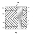
- an interlayer insulating film structure (only one connecting portion between interconnection layers is shown) 100 provided on a semiconductor substrate (not shown) formed with a number of semiconductor elements comprises a barrier cap layer 71 of silicon carbide (SiC) or the like, a carbon-containing silicon oxide (SiOC) film 72 formed on the barrier cap layer 71, a via hole 8 provided in the SiOC film 72, a trench 9 provided in a PAR (low-permittivity silicon (Si) layer 73), and a hard mask 74 of silicon oxide (SiO 2 ) covering them.
- a metal such as Cu is buried in the via hole 8 to form an electrode or interconnection 8 and, at its upper end, Cu or the like is buried in the trench 9 to form an interconnection 11.
- a multilayer interconnection structure (only one connecting portion between interconnection layers is shown) 10 provided on a semiconductor substrate (not shown) formed with a number of semiconductor elements has a first interlayer insulating film 2 in the form of a fluorocarbon film (hereinafter referred to as a CFx film) formed on a barrier cap layer 1 of silicon carbonitride (SiCN).
- a fluorocarbon film hereinafter referred to as a CFx film
- a via hole 7 is provided so as to penetrate the first interlayer insulating film 2 and the barrier cap layer 1.
- An electrode or interconnection 8 of Cu is formed in the via hole 7.
- a second interlayer insulating film 4 in the form of a fluorocarbon film is formed on the first interlayer insulating film 2 through a first adhesive layer 3 of SiCN.
- a hard mask 6 of silicon oxide (SiO 2 ) is provided on the second interlayer insulating film 4 through a second adhesive layer 5 of SiCN.
- a trench 9 is provided from the hard mask 6 to the interlayer insulating film 2 and an interconnection conductor 11 of Cu is buried in this trench.
- a thin CFx film 2a is formed by CVD on the underlayer 1 in the form of the SiCN layer by decomposition of a C 5 F 8 gas using a Xe plasma and a thick CFx film 2b is formed by CVD on the CFx film 2a by decomposition of a C 5 F 8 gas using an argon (Ar) plasma.
- the surface of the CFx film 2b is nitrided by nitrogen radicals produced by introducing an N 2 gas into an Ar gas plasma, thereby reducing outgassing from the CFx films.
- the film stripping is prevented and the permittivity can be controlled in a range of 1.7 to 2.2.
- a microwave is radiated from a radial line slot antenna (RLSA) 21 disposed through an insulator plate in the upper part of a plasma processing apparatus 102 and then is transmitted through the underlying insulator plate and a shower plate 23 into a plasma generating region.
- RLSA radial line slot antenna
- a Xe gas or an Ar gas is uniformly ejected into the plasma generating region from the upper shower plate 23 through a gas introducing pipe 13, so that a plasma is excited by the microwave radiated into the plasma generating region.
- a lower shower plate 22 is disposed in a diffusion plasma region of the microwave-excited plasma processing apparatus.
- a silicon (SiO 2 ) film can be formed on the surface of a substrate, for example, a silicon wafer, 14.
- a fluorocarbon film can be formed.
- an oxygen gas or an N 2 /H 2 or NH 3 gas be caused to flow from the upper shower plate 23 for oxidation or nitriding treatment, while, a mixed gas of an oxidizing gas and a nitriding gas, such as an O 2 /NH 3 , O 2 /N 2 O, or O 2 /NO gas, be caused to flow therefrom in the case of oxynitriding treatment.
- a mixed gas of an oxidizing gas and a nitriding gas such as an O 2 /NH 3 , O 2 /N 2 O, or O 2 /NO gas
- the substrate (e.g. silicon wafer) 14, i.e. the object to be processed, is placed in a process chamber 24 at a place where a plasma is diffused and directly irradiated, and is oxidized by oxygen radicals or the like excited by the plasma. In this event, it is desirable that the object to be processed be placed not in a space where the plasma is excited, but in a space where the plasma is diffused, in the process chamber 24.
- Exhaust gases in the process chamber 31 pass through an exhaust duct via non-illustrated exhaust ports and then are introduced into a small pump from its inlet ports.
- the electron temperature becomes substantially constant when the distance between a shower plate and an electrode becomes 30mm or more, and the electron temperature is lowered in the order of Ar, Kr, and Xe.
- an outgas measuring system 103 comprises an outgas measuring apparatus 30 and a photoion measuring apparatus.
- a sample 46 is placed in a heating furnace 40 of the photoion measuring apparatus. As indicated by an arrow 45, Ar is introduced as a carrier gas into the heating furnace 40 through an introducing pipe 47 while being adjusted to a flow rate of 100sccm by a mass flow controller 44.
- the heating furnace 40 is provided with heating heaters 41 and a photoion detector 42. Gases released from the sample 46 are introduced into the outgas measuring apparatus 30 through a pipe 48 provided with a valve 53. An exhaust pipe 52 provided with a valve 51 for exhaust is branched from the pipe 48.
- the outgas measuring apparatus 30 is provided with a discharge electrode 32.
- pipes 36a and 36b provided with vacuum pumps 37a and 37b, respectively, and an exhaust pipe 38 where the pipes 36a and 36b join together, the gases inside the outgas measuring apparatus 30 are exhausted as indicated by an arrow 39.
- pipes 34 and 35 are respectively provided on the inside of the outgas measuring apparatus 30 and at its adjacent portion where the discharge electrode 32 is provided.
- the pipe 34 is exhausted at a flow rate of 600sccm through a variable displacement control valve 61 and a mass flow meter 63 as indicated by an arrow 63.
- the pipe 35 is exhausted at a flow rate of 550sccm through a mass flow meter 62b as indicated by an arrow 64.
- the two pipes 34 and 35 join together to be a pipe 65 and are exhausted as indicated by an arrow 66.
- a pipe 33 provided with a mass flow controller 58 for introducing an Ar gas at 1 SLM as indicated by an arrow 59 is connected to the outgas measuring apparatus 30 at a position which is the same in the length direction as that of the pipe 34, but differs therefrom in the circumferential direction.
- the pipe 48 is provided with the valve 53 on a further downstream side as compared with the exhaust pipe 52 and a pipe 56 provided with a mass flow controller 57 for introducing an Ar gas for dilution at 500sccm is connected to the pipe 48 through a valve 54 on a further downstream side.
- the pipe 48 is connected to the outgas measuring apparatus 30 at a position which is the same in the length direction as that of the exhaust pipe 35, but differs therefrom in the circumferential direction.
- SiCN or SiCO is first formed as an underlayer by plasma treatment using SiH 4 /C 2 H 4 /N 2 or O 2 , or the like by the use of the apparatus shown in Fig. 4 .
- organic silane may be used instead of silane gas (SiH 4 )/ethylene (C 2 H 4 ).
- a thin first CFx film 2a of 5 to 10nm is formed on the underlayer 1 by a Xe plasma using a fluorocarbon gas as a reactive gas.
- fluorocarbon gas as the reactive gas, use can be made of unsaturated aliphatic fluoride expressed by a general formula C n F 2n (where n is an integer of 2 to 8) or C n F 2n-2 (n is an integer of 2 to 8), but is preferably made of fluorocarbon expressed by a general formula C 5 H 8 , such as carbon fluoride containing octafluoropentyne, octafluoropentadiene, octafluorocyclopentene, octafluoromethylbutadiene, octafluoromethylbutyne, fluorocyclopropene, or fluorocyclopropane, or carbon fluoride containing fluorocyclobutene or fluorocyclobutane.
- fluorocarbon expressed by a general formula C 5 H 8
- a second CFx film 2b having a thickness of 380 to 500nm is formed on the first CFx film 2a by an Ar plasma using a C 5 F 8 gas as a reactive gas. Since the permittivity of a CFx film is reduced when formed using a plasma of Ar gas, this makes it possible to reduce the permittivity of the CFx film 2 to as low as 1.7 to 2.2.
- the surface of the CFx film is nitrided by an Ar/N 2 plasma or an N 2 plasma. This makes it possible to reduce outgassing from the CFx films.
- annealing is performed after the film formation and before the surface nitriding.
- the annealing may be performed in the plasma chamber with the substrate as it is without exposing the substrate to the atmosphere or may be performed using a separate annealing apparatus.
- an atmosphere is set to an inert gas atmosphere and the pressure may be set to an atmospheric pressure but is preferably set to a reduced pressure of about 1 Torr.
- the fluorocarbon film be irradiated with an Ar plasma before or after the annealing.
- a first interlayer insulating film 2 shown in Fig. 3 is formed using a barrier cap layer 1 as an underlayer.
- a via hole 7 is formed in the first interlayer insulating film 2 by etching.
- a film of a fluoride of nickel, preferably a nickel difluoride (referred to as NiF 2 ) film is formed on the inner wall of the via hole 7 by forming a film of nickel by PVD and then fluorinating it, or is directly formed thereon by MOCVD.
- an SiCN layer or a carbon-containing silicon oxide (SiCO) layer is formed as an underlayer 3 in the form of an adhesive layer and, thereon, an interlayer insulating film 4 comprising a first and a second CFx film is formed in the same manner as shown in Fig. 3 .
- an SiCN layer or an SiCO layer is further formed as an underlayer 3 for adhesion and, on this underlayer 3, an SiO 2 or SiCO layer is formed as a hard mask layer 6.
- the SiO 2 layer can be formed by introducing a mixed gas of Ar and O 2 from the upper shower plate 23 and introducing an SiH 4 gas from the lower shower plate 22 in the plasma processing apparatus 102 shown in Fig. 4 .
- the SiCO layer is the same as described before.
- a trench 9 is formed by etching, a non-illustrated NiF 2 barrier layer is formed on the inner wall surface of the trench 9, and Cu is filled as a metal in the trench 9 to form an interconnection conductor 11, so that the interconnection structure 10 is completed.
- SiFx gases are produced by reactions at the interface between a layer of Si, SiO 2 , Si 3 N 4 , or the like and a CFx film.
- Table 1 below shows the ionization potentials of outgases. As shown in Table 1, it is seen that the ionization potential of SiFx increases in the order of SiF, SiF 3 , SiF 2 , and SiF 4 .
- SiFx gases The release of SiFx gases depends on an underlayer in the initial film formation.
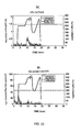
- Fig. 7 represents diagrams showing the temperature dependence of SiFx outgassing per different underlayer, wherein the left scale shows the outgas amount when the temperature represented by the right scale is applied, with the lapse of time, to (a) a CFx film formed on a Si underlayer (CFx/Si), (b) a CFx film formed on an SiO 2 underlayer (CFx/SiO 2 ), and (c) a CFx film formed on an Si 3 N 4 underlayer (CFx/Si 3 N 4 ).
- the SiFx outgassing changes by changing the underlayer. It has been found that the reactions at the CFx/underlayer interface are such that the outgassing decreases in amount in the order of Si, SiO 2 , and Si 3 N 4 .
- Fig. 8 is a diagram showing the temperature dependence of SiF-based outgas amounts. As shown in Fig. 8 , it is seen that reactions occur at the interface between SiO 2 and CFx to produce SiFx outgases. Therefore, it is understood that it is essential to suppress the interfacial reactions. A further detailed investigation was made of SiF 4 .
- Fig. 9 is a diagram showing time-dependent changes of SiF 4 spectra. Referring to Fig. 9 , it is seen that, in the outgas measurement using a standard CFx film, when the temperature is raised with CFx/SiO 2 , SiF 4 is produced and continues to be produced for 16 hours. Therefore, it is seen that it is essential to suppress the reactions at the CFx film/SiO 2 interface.
- Fig. 10 represents diagrams showing the temperature dependence of SiF-based outgas amounts, wherein (a) shows the temperature dependence of outgas amounts in the case of film formation using Ar and (b) shows it in the case of film formation using Xe.
- Fig. 11 is a diagram showing the temperature dependence of SiFx gas amounts when an underlayer is made of Si.
- the conditions were such that, using C 5 F 8 as a reactive gas, film formation was performed by plasma treatment using Xe at 26.6Pa (200mTorr) for 5 seconds, then film formation was performed by plasma treatment using Ar at 26.6Pa (200mTorr) and, after annealing, treatment was performed using Ar at 26.6Pa (200mTorr) for 5 seconds.
- Fig. 11 it has been found that the SiFx gases can be reduced by using Xe in the initial film formation.
- Fig. 12 represents diagrams showing the temperature dependence of SiFx-based outgas amounts, wherein (a) shows the outgas amounts from a CFx film obtained by treatment with C 5 F 8 /Xe at 26.6Pa (200mTorr) for 5 seconds, then treatment with C 5 F 8 /Ar at 26.6Pa (200mTorr) and, after annealing, treatment with Ar at 26.6Pa (200mTorr) for 5 seconds and (b) shows the outgas amounts from a CFx film obtained by treatment (5 seconds) in which a Xe plasma is on and C 5 F 8 is introduced, then, after the introduction of C 5 F 8 is off and the Xe plasma is off, Ar/C 5 F 8 treatment for 3 minutes and then Ar+N 2 treatment for 5 seconds.
- Fig. 13 shows the temperature dependence of SiFx outgas amounts when an underlayer is made of Si.
- treatment was performed for 5 seconds while a Xe plasma was on and a C 5 F 8 gas was introduced, then the C 5 F 8 gas was off and the Xe plasma was off, then Ar/C 5 F 8 treatment was performed for 3 minutes, and subsequently, Ar+N 2 surface nitriding treatment was performed for 5 seconds. From Fig. 13 , it is seen that the SiFx outgas amounts can be reduced by changing the sequence.
- Fig. 14 is a diagram showing the TDS outgas spectra of a CFx film of 120nm formed on a Si underlayer. As shown in Fig. 14 , it is seen that when the temperature is raised at a heating rate of 60°C/min from room temperature to 400°C, CF-based outgases and so on are produced.
- Fig. 15 is a diagram showing the temperature dependence of CFx outgas amount, after annealing, of a CF film formed on an SiO 2 underlayer. As shown in Fig. 15 , it has been found that, by removing insufficiently bonded components through annealing, subsequent decomposition reactions do not occur, thus confirming that the annealing is necessary.
- Fig. 16 is a diagram showing the temperature dependence of released water amount, after CF-film annealing, of a CF film formed on an SiO 2 underlayer in the same manner. As shown in Fig. 16 , it has been found that, once heated, there is no generation of water in an in-situ process, and thus it is seen that the in-situ process is essential.
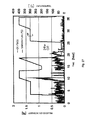
- Fig. 17 is a diagram showing the fluorocarbon outgas characteristics after Ar/N 2 plasma treatment using the apparatus of Fig. 5 and the results of thermal desorption spectrometry (TDS) measurement.
- the heating rate is 0.17°C/sec.
- the sample shown in Fig. 5 shows the outgas characteristics of a CFx film formed at 220°C using straight-chain C 5 F 8 as a reactive gas shown in Fig. 4 and then in-situ annealed at 330°C.
- the heating was stopped after 40 seconds from the start of the heating, so that the temperature was maintained at a constant value of 400°C. It is seen that the release extremely increases near 350°C and becomes maximum at a temperature somewhat lower than 400°C.
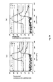
- Fig. 18 represents diagrams showing the temperature dependence of CFx-based outgas amount in the case where C 5 F 8 is introduced in Ar-plasma treatment, then the introduction is stopped in the plasma treatment, and then the Ar-plasma treatment is stopped, wherein (a) shows the relationship between the relative intensity of CFx outgas and the time and (b) shows the relationship between the H 2 O concentration (ppb/cm 2 ) for released water and the time.
- Fig. 18(a) and Fig. 18(b) it is seen that dangling components are reduced by causing the material gas to flow in the plasma treatment. Further, it is seen that the released water is also reduced and thus the effective surface area is reduced.
- Fig. 19 represents diagrams showing the annealing temperature dependence of outgas amounts of the CFx film, wherein (a) shows the outgas amount of a CF-based gas and (b) shows the outgas amount of an H 2 O gas. From Figs. 19(a) and (b) , it is seen that, by removing insufficiently bonded components through annealing at 400°C, subsequent decomposition reaction processes do not occur. Further, it is seen that, once heated, there is no generation of water in an in-situ process, and thus it is seen that the in-situ process is essential for the annealing.
- Fig. 20 represents diagrams showing the spectral of various outgases according to a difference in leaving time of a CFx film, wherein (a) shows the results of measurement after being left standing in the atmosphere for 12 hours after annealing at 400°C and (b) shows the results of measurement after being left standing in the atmosphere for 48 hours without annealing. From a comparison between Figs. 30 (a) and (b) , an HF outgas increases due to being left standing in the atmosphere. This represents that water in the atmosphere and the CFx film reacted with each other.
- Fig. 21 represents diagrams showing the temperature dependence of Si-based outgas amount, wherein (a) shows the temperature dependence of CFx outgassing and (b) shows the temperature dependence of water release.
- an Ar plasma was irradiated for 5 seconds after the treatment, and then annealing was carried out.
- the CFx outgassing is reduced to 2/3 so that insufficiently bonded CFx is reduced.
- the water release is also reduced to 1/2 and thus the effective surface area is reduced.
- Fig. 22 represents diagrams showing the surface nitriding effects, wherein (a) and (b) show the CFx outgassing effect and the water release effect, respectively, when the Ar/N 2 plasma was irradiated for 5 seconds after the annealing.
- the CFx gas is reduced to 1/3 as compared with the standard condition by the Ar/N 2 plasma irradiation after the annealing.
- the released water is also reduced to 1/3 and thus the effective surface area is reduced.
- Fig. 23 shows the results of measurement of a sample formed with a CFx film and subjected to Ar/N 2 plasma irradiation after annealing like in Fig. 17 , using an X-ray photoelectron spectrometer (ESCA: Electron Spectroscopy for Chemical Analysis). From the results of Fig. 23 , it has been found that N atoms were detected only in several nm from the surface and thus the outgassing was reduced by the surface quality improvement by the annealing. The permittivity of the CFx film was 2.04 before the outgassing while it was 2.08 after the outgassing, and thus no large change was observed.
- ESA Electron Spectroscopy for Chemical Analysis
- Fig. 24 represents diagrams showing the film forming condition dependence of outgas amounts of a CFx film, wherein (a) shows CF-based outgassing and (b) shows H 2 O-based outgassing.
- a shows CF-based outgassing
- b shows H 2 O-based outgassing.
- the CFx outgassing is reduced by Ar/N plasma irradiation for 5 seconds after annealing at 400°C to thereby Ar/N 2 -treat the surface (surface nitriding). It is seen that the CFx outgassing is reduced to 1/3 as compared with no annealing.
- Fig. 25 represents diagrams showing the results of outgassing in the case of Ar/N 2 plasma treatment after annealing a CFx film formed to 400nm, wherein (a) shows the results with no nitriding being the normal condition and (b) shows the results with nitriding. It is seen that the outgassing is small in amount by the Ar/N 2 nitriding treatment.
- Fig. 26 is a diagram showing the outgas TDS spectra of an SiCN film in-situ formed on a CFx film (SiCN/CFx) formed on a Si underlayer. As shown in Fig. 26 , it is seen that outgassing is reduced by forming the SiCN film as a cap layer on the CFx film.
- Fig. 27 shows the temperature dependence of CF-based outgas amount when a CFx film is formed on SiO 2 at 200°C and annealed in Ar at 350°C for 30 minutes. Referring to Fig. 27 , it is observed that, by removing insufficiently bonded components through annealing, decomposition reactions do not occur even if the temperature is raised to 400°C thereafter, and the outgas amount of CF-based gas is reduced.
- Fig. 28 is a diagram showing the temperature dependence of outgas amount in the case where nitriding treatment is performed by an Ar/N 2 plasma at 200°C after film formation at 200°C and annealing at 350°C. As shown in Fig. 28 , it has been found that when a CFx film is formed on SiO 2 , then annealed at 350°C, and then irradiated with an Ar/N 2 plasma at 200°C, the outgassing is extremely reduced and thus the film surface quality improvement effect is large.
- Fig. 29 is a diagram showing the outgas amount in the case where a CFx film is formed on a Si substrate at 350°C and no annealing is carried out.
- Fig. 30 is a diagram showing the outgas amount in the case where a CFx film is formed on a Si substrate at 350°C, then annealed at 350°C, and then the surface thereof is nitrided by an Ar/N 2 plasma at 200°C.
- Fig. 30 shows that the outgassing is suppressed and the surface quality is improved by annealing and then nitriding the surface.
- Fig. 31 is a diagram showing the outgas amount in the case where a CFx film is formed on a Si substrate at 400°C and no annealing is carried out. As shown in Fig. 31 , the outgassing is observed after forming the CFx film on Si at 400°C and then annealing it at 350°C.
- Fig. 32 is a diagram showing the outgas amount in the case where a CFx film is formed on a Si substrate at 400°C and then irradiated with an Ar/N 2 plasma without annealing. As shown in Fig. 32 , it is seen that the outgassing increases when the nitriding treatment is performed by the Ar/N 2 plasma at 400°C.
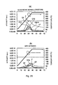
- Figs. 33(a) and (b) are diagrams showing an NiF 2 film forming method and a Ni film forming method for comparison, respectively.
- Figs. 34(a) and (b) are graphs showing the compositions of a Ni film and an NiF 2 film, respectively.
- Figs. 34(a) and (b) show that a Ni film (after annealing at 350°C) and an NiF 2 film are formed on SiO 2 , respectively.
- Figs. 35(a) and (b) show the states before and after annealing in the case where a Ni film of 50nm is formed as a barrier metal layer and a Cu film is formed thereon, wherein it is shown that Ni diffuses into the Cu film and Cu diffuses into the Ni film.
- Figs. 36(a) and (b) show that when an NiF 2 film of 50nm is formed as a barrier (metal) layer, no diffusion of Cu or Ni occurs before and after annealing and thus, when the NiF 2 film is used as the barrier layer, it completely functions as a barrier to Cu.
- Fig. 37 is a diagram showing the results of elemental analysis in the depth direction after the formation of the NiF 2 film.
- Fig. 38 represents sectional SEM photographs showing a metallographic structure in which a Cu layer is formed on an NiF 2 layer, wherein the right photograph enlarges a portion of the left photograph.
- Fig. 39(a) and Fig. 39(b) are graphs showing the results of mutual diffusion evaluation of a sample having an NiF 2 film of 10nm formed as a barrier layer, wherein (a) is a diagram showing the state before a mutual diffusion test (before annealing at 350°C) and (b) is a diagram showing the state after the mutual diffusion test (after annealing at 350°C). Figs. 39(a) and (b) show that there is no diffusion of Cu or Ni even after the annealing and thus it completely functions as a barrier to Cu.
- an interlayer insulating film comprising a CFx film according to this invention and its manufacturing method and an interconnection structure and its manufacturing method are optimum for a semiconductor device or a wiring board having a low-permittivity interlayer insulating film and an interconnection structure, or an electronic device including them.
Landscapes
- Engineering & Computer Science (AREA)
- Physics & Mathematics (AREA)
- Power Engineering (AREA)
- General Physics & Mathematics (AREA)
- Computer Hardware Design (AREA)
- Microelectronics & Electronic Packaging (AREA)
- Condensed Matter Physics & Semiconductors (AREA)
- Manufacturing & Machinery (AREA)
- Plasma & Fusion (AREA)
- Chemical & Material Sciences (AREA)
- Chemical Kinetics & Catalysis (AREA)
- Internal Circuitry In Semiconductor Integrated Circuit Devices (AREA)
- Formation Of Insulating Films (AREA)
- Chemical Vapour Deposition (AREA)
Abstract
Description
- This invention relates to a multilayer interconnection structure, particularly an interlayer insulating film structure, of a board ,such as a semiconductor-element or semiconductor-chip mounting board or a wiring board and further relates to a semiconductor device having the multilayer interconnection structure, a wiring board having the multilayer interconnection structure, and an electronic device including them. Moreover, this invention relates to a method of manufacturing the multilayer interconnection structure and methods of manufacturing the semiconductor device having the multilayer interconnection structure, the wiring board having the multilayer interconnection structure, and the electronic device including them.
- Conventionally, an interlayer insulating film is formed for insulation between interconnection layers in a multilayer interconnection structure on a semiconductor substrate or the like.
- In such a multilayer interconnection structure, a problem of signal delay due to the parasitic capacitance between interconnections and the interconnection resistance has become unignorable and it has been required to use an interlayer insulating film having a low permittivity (Low-k).
- As such an interlayer insulating film, attention has been paid to the fact that a fluorocarbon film (hereinafter referred to as a CFx film) has a very low permittivity and thus can reduce the parasitic capacitance between interconnections. However, the CFx film is very weak against water and poor in adhesion. Therefore, the CF film is formed on an underlayer such as an SiCN layer, an Si3N4 layer, or an SiO2 layer, but there has been a problem in the bottom and top surfaces of the CF film (i.e. the beginning and end of the film formation).
- Conventionally, a CFx film is formed by the use of a plasma processing apparatus using a fluorocarbon gas (referred to as a CFx gas, e.g. a C5F8 gas), for example, as described in
Patent Document 1. - As described in
Patent Document 2, this CFx gas is originally used for etching and thus there has been a problem that if the plasma treatment temperature is high, an underlayer is etched to produce a silicon fluoride (SiF4) gas. - Further, there has been a problem that water and gases such as CFx and SiF4 are released from the surface of the formed CF film to form a contamination source.
-
Patent Document 3 describes that a formed CFx film is annealed in an N2 atmosphere at 400°C to 450°C, so that outgassing after the film formation is small in amount. - Further, plasma treatment is performed using a single rare gas when forming an oxide film, a nitride film, an oxynitride film, or the like as an underlying metal on a silicon semiconductor. In the case of using a single rare gas, use is made of a krypton (Kr) gas or a xenon (Xe) gas having a large sectional area for collision with electrons and a low plasma electron temperature for the purpose of reducing plasma damage to post-treatment (e.g. see Patent Document 4).
-
- Patent Document 1: Japanese Unexamined Patent Application Publication (
JP-A) No. 2002-220668 - Patent Document 2: Japanese Unexamined Patent Application Publication (
JP-A) No. 2002-16050 - Patent Document 3: Japanese Unexamined Patent Application Publication (
JP-A) No. H11-162962 - Patent Document 4: Japanese Unexamined Patent Application Publication (
JP-A) No. 2002-261091 - It is therefore an object of this invention to provide an interlayer insulating film of a semiconductor device or the like, which has a low permittivity, is free from generation of gases such as CFx and SiF4, and is stable.
- It is another object of this invention to provide a method of manufacturing an interlayer insulating film of a semiconductor device or the like, which has a low permittivity, is free from generation of gases such as CFx and SiF4, and is stable.
- It is still another object of this invention to provide an interconnection structure of a semiconductor device or the like, comprising an interlayer insulating film having a low permittivity and being free from generation of gases such as CFx and SiF4 and stable.
- It is a further object of this invention to provide a method of manufacturing an interconnection structure of a semiconductor device or the like, comprising an interlayer insulating film having a low permittivity and being free from generation of gases such as CFx and SiF4 and stable.
- It is still another object of this invention to provide methods of manufacturing the above interlayer insulating film and the above interconnection structure.
- According to one aspect of the present invention, there is provided an interlayer insulating film which includes an insulating film formed on an underlayer, said interlayer insulating film having an effective permittivity of 3 or less.
- In the aspect of the present invention, it is preferable that the insulating film includes a first fluorocarbon film formed on the underlayer and a second fluorocarbon film formed on the first fluorocarbon film and having a permittivity lower than that of the first fluorocarbon film.
- In the interlayer insulating film, it is also preferable that the first fluorocarbon film has a thickness of 5 to 10nm and the second fluorocarbon film has a thickness of 280 to 500nm. Furthermore, it is preferable that each of the first and the second fluorocarbon films has a low permittivity. Specially, it is preferable that the permittivity of the second fluorocarbon film is 1.5 to 2.5. Moreover, it is preferable that the underlayer includes at least one of an SiCN layer, a silicon nitride (Si3N4) layer, an SiCO layer, and an SiO2 layer formed on a base body. Specially, it is preferable that the first fluorocarbon film is provided for preventing generation of a fluorosilane gas produced by a reaction with the underlayer.
- In addition, the first fluorocarbon film may be formed by CVD using a plasma generated by using a Xe or Kr gas. On the other hand, the second fluorocarbon film may be formed by CVD using a plasma generated by using an Ar gas.
- It is also preferable that a surface of the second fluorocarbon film is nitrided and a thickness of a nitrided portion of the surface is 1 to 5nm, preferably 2 to 3nm.
- It is preferable that a film formed on the insulating film and made of at least one of Si3N4, SiCN, SiCO is provided.
- According to another aspect of the present invention, there is provided a method of forming a fluorocarbon film on an underlayer using a fluorocarbon gas and two or more kinds of rare gas. The method includes a first step of forming a first fluorocarbon film on the underlayer by a plasma generated by using a rare gas other than an Ar gas and a second step of forming a second fluorocarbon film on the first fluorocarbon film by a plasma generated by using an Ar gas.
- In the method according to the aspect of the present invention, it is preferable that the first fluorocarbon film is formed up to a thickness of 5 to 10nm and the second fluorocarbon film is formed up to a thickness of 280 to 500nm on the first fluorocarbon film. Specially, it is preferable that the second fluorocarbon film has a permittivity lower than that of the first fluorocarbon film.
- In addition, It is preferable that the underlayer is a layer including at least one of an SiCN layer, an Si3CN4 layer, an SiO2 layer, and an SiCO layer formed on a base body and that the rare gas used in the first step is a Xe gas.
- Furthermore, the film of at least one kind of Si3N4, SiCN, and SiCO may be formed by adding at least one of a nitrogen gas and an oxidizing gas to the rare gas and flowing a SiH4 gas as a reactive gas.
- According to still another aspect of the present invention, there is provided a method of manufacturing a multilayer interconnection structure of a semiconductor device or the like. The method includes a step of forming a fluorocarbon film as at least portion of an interlayer insulating film, a step of annealing the fluorocarbon film, and a step of nitriding a surface of the fluorocarbon film.
- In the present invention, it is preferable that the annealing step is performed in an inert gas without exposure to the atmosphere. It is also preferable that the nitriding step is performed in a plasma using an Ar gas and using an N2 gas or in a plasma using an N2 gas. In the latter case, it is preferable that the nitriding step is performed at a temperature of 200°C or higher, more preferably at a temperature of 300°C to 400 °C.
- Furthermore, it is preferable that the method further includes, before or after the annealing step, a step of irradiating the surface of the fluorocarbon film with a rare gas plasma.
- According to yet another aspect of the present invention, there is provided an interconnection structure which includes an interlayer insulating film having an insulating film formed on an underlayer, a contact hole formed in the interlayer insulating film, and a metal filled in the contact hole, the interlayer insulating film having an effective permittivity of 3 or less.
- In the aspect of the present invention, it is preferable that the metal filled in the contact hole contains copper and a barrier layer including at least a layer of a fluoride of nickel is interposed between the interlayer insulating film and copper. The fluoride of nickel is, for example, nickel difluoride, but is not limited thereto. This fluoride of nickel is formed by MOCVD or is formed by forming a film of nickel by PVD (Physical Vapor Deposition) and then fluorinating the film. The interlayer insulating film is preferably a fluorocarbon film.
- It is preferable that the insulating film includes a first fluorocarbon film formed on the underlayer and a second fluorocarbon film formed on the first fluorocarbon film and having a permittivity lower than that of the first fluorocarbon film, and that the first fluorocarbon film has a thickness of 5 to 10nm while the second fluorocarbon film has a thickness of 280 to 500nm. Specially, it is preferable that the permittivity of the second fluorocarbon film is 1.5 to 2.5. Furthermore, it is preferable that the underlayer includes at least one of an SiCN layer, an Si3CN4 layer, and an SiO2 layer formed on a base body. Herein, the first fluorocarbon film is provided for preventing generation of a silicon fluoride gas produced by a reaction with the underlayer.
- Furthermore, it is preferable that the interconnection structure further includes a film formed on the fluorocarbon film and containing at least one of Si3N4, SiCN, and SiCO, and that a nitrided film is provided at a surface portion of the second fluorocarbon film.
- According to a further aspect of the present invention, there is provided a method of manufacturing an interconnection structure. The method includes a first step of forming a first fluorocarbon film on an underlayer using a fluorocarbon gas and a rare gas whose plasma has an electron temperature lower than that of Ar, and a second step of forming a second fluorocarbon film on the first fluorocarbon film by a plasma generated by using an Ar gas.
- Herein, it is preferable that the first fluorocarbon film is formed in a thickness of 5 to 10nm while the second fluorocarbon film is formed in a thickness of 280 to 500nm. Furthermore, it is also preferable that each of the first and the second fluorocarbon films has a low permittivity. Specially, it is preferable that the permittivity of the second fluorocarbon film is adjusted to 1.5 to 2.5.
- Furthemore, it is preferable that the underlayer includes at least one of an SiCN layer, an Si3N4 layer, an SiCO layer, and an SiO2 layer formed on a base body. It is also preferable that the rare gas used in the first step is a Xe gas.
- Moreover, a film of at least one of Si3N4 or SiCN, and SiCO may be formed by adding at least one of a nitriding gas and an oxidizing gas to the rare gas, and flowing an SiH4 gas as a reactive gas. It is preferable that a surface of the second fluorocarbon film is nitrided.
- In the aspect of the present invention, it is preferable that the method includes, in addition to the first and the second steps, a step of forming a contact hole in the fluorocarbon films and a step of filling a metal in the contact hole. It is also preferable that the method further includes a step of forming a barrier layer for preventing diffusion of the metal filled in the contact hole.
- Accoding to a yet further aspect of the present invention, there is provided a method of cleaning a chamber, comprising, after generating a plasma in a pressure-reduced chamber to form a fluorocarbon film on a substrate placed in the chamber, generating a plasma using a mixed gas of hydrogen and oxygen in the chamber, thereby cleaning an inner wall of the chamber.
- According to this invention, it is possible to provide an interlayer insulating film of a semiconductor device, which has a low permittivity, is free from generation of gases such as CFx and SiF4, and is stable, and a method of manufacturing it.
- Further, according to this invention, it is possible to provide an interconnection structure comprising such an interlayer insulating film and a method of manufacturing it.
- Further, according to this invention, by first forming a fluorocarbon film by plasma CVD using a Xe or Kr gas, it is possible to reduce outgassing of SiF-based gases and further to prevent stripping of the fluorocarbon film. Then, by forming a main portion of the fluorocarbon film by CVD in an Ar gas plasma, it is possible to reduce the effective permittivity of the fluorocarbon film.
- Further, according to this invention, by nitriding the surface of the fluorocarbon film, there is an effect of largely reducing outgassing and there is also an effect of preventing stripping of an insulating film formed on the fluorocarbon film.
- Further, according to this invention, by providing a barrier layer of nickel difluoride on the inner surface of a via hole or a contact hole, it is possible to prevent Cu in the hole from diffusing into the barrier layer.
-
-
Fig. 1 is a diagram showing a conventional interlayer insulating film structure of a semiconductor device according to prior art. -
Fig. 2 is a diagram showing an interconnection structure according to an embodiment of this invention. -
Fig. 3 is a schematic sectional view showing the structure of an interlayer insulating film used in the interconnection structure ofFig. 2 . -
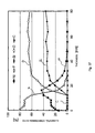
Fig. 4 is a schematic sectional view showing a plasma processing apparatus according to an embodiment of this invention. -
Fig. 5 is a diagram showing the relationship between the distance between a shower plate and an electrode, and the electron density (ev) for an Ar plasma, a Kr plasma, and a Xe plasma. -
Fig. 6 is a diagram showing a schematic structure of an outgas measuring test apparatus. -
Fig. 7 represents diagrams showing the underlayer dependence of SiFx outgassing, wherein (a) shows a CFx film formed on a Si underlayer (CFx/Si), (b) shows a CFx film formed on an SiO2 underlayer (CFx/SiO2), and (c) shows a CFx film formed on an Si3N4 underlayer (CFx/Si3N4). -
Fig. 8 is a diagram showing the temperature dependence of SiF-based gas amounts. -
Fig. 9 is a diagram showing time-dependent changes of SiF4 spectra. -
Fig. 10 represents diagrams showing the temperature dependence of SiF-based outgas amounts, wherein (a) shows the temperature dependence of outgas amounts in the case of film formation using Ar and (b) shows it in the case of film formation using Xe. -
Fig. 11 is a diagram showing the temperature dependence of SiFx gas amounts when an underlayer is made of Si. -
Fig. 12 represents diagrams showing the temperature dependence of SiFx-based outgas amounts, wherein (a) shows the outgas amounts from a CFx film obtained by treatment with C5F8/Xe at 26.6Pa (200mTorr) for 5 seconds, then treatment with C5F8/Ar at 26.6Pa (200mTorr) and, after annealing, treatment with Ar at 26.6Pa (200mTorr) for 5 seconds and (b) shows the outgas amounts from a CFx film obtained by treatment (5 seconds) in which a Xe plasma is on and C5F8 is introduced, then, after the introduction of C5F8 is off and the Xe plasma is off, Ar/C5F8 treatment for 3 minutes and then Ar+N2 treatment for 5 seconds. -
Fig. 13 shows the temperature dependence of SiFx outgas amounts when an underlayer is made of Si. -
Fig. 14 is a diagram showing the TDS outgas spectra of a CFx film of 120nm formed on a Si underlayer. -
Fig. 15 is a diagram showing the temperature dependence of CFx outgas amount, after annealing, of a CF film formed on an SiO2 underlayer. -
Fig. 16 is a diagram showing the temperature dependence of released water amount, after CF-film annealing, of a CF film formed on an SiO2 underlayer in the same manner. -
Fig. 17 is a diagram showing the fluorocarbon outgas characteristics after Ar/N2 plasma treatment using the apparatus ofFig. 5 and the results of thermal desorption spectrometry (TDS) measurement. -
Fig. 18 represents diagrams showing the temperature dependence of CFx-based outgas amount in the case where C5F8 is introduced in Ar-plasma treatment, then the introduction is stopped in the plasma treatment, and then the Ar-plasma treatment is stopped, wherein (a) shows the relationship between the relative intensity of CFx outgas and the time and (b) shows the relationship between the H2O concentration (ppb/cm2) for released water and the time. -
Fig. 19 represents diagrams showing the annealing temperature dependence of outgas amounts of a CFx film, wherein (a) shows the outgas amount of a CF-based gas and (b) shows the outgas amount of an H2O gas. -
Fig. 20 represents diagrams showing the spectral of various outgases according to a difference in leaving time of a CFx film, wherein (a) shows the results of measurement after being left standing in the atmosphere for 12 hours after annealing at 400°C and (b) shows the results of measurement after being left standing in the atmosphere for 48 hours without annealing. -
Fig. 21 represents diagrams showing the temperature dependence of Si-based outgas amount, wherein (a) shows the temperature dependence of CFx outgassing and (b) shows the temperature dependence of water release. -
Fig. 22 represents diagrams showing the surface nitriding effects, wherein (a) and (b) show the CFx outgassing effect and the water release effect, respectively, when an Ar/N2 plasma was irradiated for 5 seconds after annealing. -
Fig. 23 shows the results of measurement of a sample formed with a CFx film and subjected to Ar/N2 plasma irradiation after annealing like inFig. 17 , using an X-ray photoelectron spectrometer (ESCA: Electron Spectroscopy for Chemical Analysis). -
Fig. 24 represents diagrams showing the film forming condition dependence of outgas amounts of a CFx film, wherein (a) shows CF-based outgassing and (b) shows H2O-based outgassing. -
Fig. 25 represents diagrams showing the results of outgassing in the case of Ar/N2 plasma treatment after annealing a CFx film formed to 400nm, wherein (a) shows the results with no nitriding being the normal condition and (b) shows the results with nitriding. It is seen that outgassing is small in amount by the Ar/N2 nitriding treatment. -
Fig. 26 is a diagram showing the outgas TDS spectra of an SiCN film in-situ formed on a CFx film (SiCN/CFx) formed on a Si underlayer. -
Fig. 27 is a diagram showing the temperature dependence of CF-based outgas amount when a CFx film formed at 200°C is annealed at 350°C. -
Fig. 28 is a diagram showing the temperature dependence of outgas amount in the case where a film is formed at 200°C and then annealed at 350°C and, further, the surface thereof is nitrided by an Ar/N2 plasma at 200°C. -
Fig. 29 is a diagram showing the outgas amount in the case where a CFx film is formed on a Si substrate at 350°C and no annealing is carried out. -
Fig. 30 is a diagram showing the outgas amount in the case where a CFx film is formed on a Si substrate at 350°C, then annealed at 350°C, and then the surface thereof is nitrided by an Ar/N2 plasma at 200°C. -
Fig. 31 is a diagram showing the outgas amount in the case where a CFx film is formed on a Si substrate at 400°C and no annealing is carried out. -
Fig. 32 is a diagram showing the outgas amount in the case where a CFx film is formed on a Si substrate at 400°C and then the surface thereof is nitrided by an Ar/N2 plasma at 400°C without annealing. -
Figs. 33 (a) and (b) are diagrams showing an NiF2 film forming method and a Ni film forming method for comparison, respectively. -
Figs. 34 (a) and (b) are graphs showing the compositions of a Ni film and an NiF2 film, respectively. -
Figs. 35 (a) and (b) are diagrams showing the states before and after annealing in the case where a Ni film of 50nm is formed as a barrier metal layer and a Cu film is formed thereon. -
Figs. 36 (a) and (b) are diagrams showing diffusion of Cu, Ni, and so on before and after annealing when an NiF2 film of 50nm is formed as a barrier (metal) layer. -
Fig. 37 is a diagram showing the results of elemental analysis in the depth direction after the formation of the NiF2 film. -
Fig. 38 represents sectional SEM photographs showing a metallographic structure in which a Cu layer is formed on an NiF2 layer, wherein the right photograph enlarges a portion of the left photograph. -
Figs. 39 (a) and (b) are graphs showing the results of mutual diffusion evaluation of a sample having an NiF2 film of 10nm formed as a barrier layer, wherein (a) is a diagram showing the state before a mutual diffusion test (before annealing at 350°C) and (b) is a diagram showing the state after the mutual diffusion test (after annealing at 350°C). -
- 1
- barrier cap layer
- 2
- first interlayer insulating film
- 2a
- CFx film
- 2b
- CFx film
- 3
- first adhesive layer
- 4
- second interlayer insulating film
- 5
- second adhesive layer
- 6
- hard mask
- 7
- via hole
- 8
- electrode
- 9
- trench
- 10
- interconnection structure
- 11
- interconnection conductor (Cu)
- 12
- antenna
- 13
- gas introducing pipe
- 14
- silicon wafer
- 21
- insulator plate
- 22
- lower shower plate
- 23
- upper shower plate
- 24
- process chamber
- 26
- introducing pipe
- 30
- outgas measuring apparatus
- 31
- process chamber
- 32
- discharge electrode
- 33
- pipe
- 34, 35
- pipe
- 36a, 36b
- pipe
- 37a, 37b
- vacuum pump
- 38
- exhaust pipe
- 39
- arrow
- 40
- heating furnace
- 41
- heating heater
- 42
- photoion detector
- 44
- mass flow controller
- 45
- arrow
- 46
- sample
- 47
- introducing pipe
- 48
- pipe
- 51
- valve
- 52
- exhaust pipe
- 53
- valve
- 54
- valve
- 56
- pipe
- 57
- mass flow controller
- 58
- mass flow controller
- 59
- arrow
- 61
- variable displacement control valve
- 62a, 62b
- mass flow meter
- 63
- arrow
- 64
- arrow
- 65
- pipe
- 66
- arrow
- 71
- barrier cap layer
- 72
- SiOC film
- 73
- PAR (low-permittivity Si layer)
- 74
- hard mask
- 100
- interconnection structure
- 102
- plasma processing apparatus
- 103
- outgas measuring system
- In order to facilitate understanding of this invention, a convnertional interlayer insulating film structure of a semiconductor device according to prior art will be described with reference to
Fig. 1 before describing an embodiment of this invention. - Referring to
Fig. 1 , in the semiconductor device according to prior art, an interlayer insulating film structure (only one connecting portion between interconnection layers is shown) 100 provided on a semiconductor substrate (not shown) formed with a number of semiconductor elements comprises abarrier cap layer 71 of silicon carbide (SiC) or the like, a carbon-containing silicon oxide (SiOC)film 72 formed on thebarrier cap layer 71, a viahole 8 provided in theSiOC film 72, atrench 9 provided in a PAR (low-permittivity silicon (Si) layer 73), and ahard mask 74 of silicon oxide (SiO2) covering them. A metal such as Cu is buried in the viahole 8 to form an electrode orinterconnection 8 and, at its upper end, Cu or the like is buried in thetrench 9 to form aninterconnection 11. - Now, the embodiment of this invention will be described with reference to the drawings.
- As shown in
Fig. 2 , in a semiconductor device according to the embodiment of this invention, a multilayer interconnection structure (only one connecting portion between interconnection layers is shown) 10 provided on a semiconductor substrate (not shown) formed with a number of semiconductor elements has a firstinterlayer insulating film 2 in the form of a fluorocarbon film (hereinafter referred to as a CFx film) formed on abarrier cap layer 1 of silicon carbonitride (SiCN). - A via
hole 7 is provided so as to penetrate the firstinterlayer insulating film 2 and thebarrier cap layer 1. An electrode orinterconnection 8 of Cu is formed in the viahole 7. Further, a secondinterlayer insulating film 4 in the form of a fluorocarbon film is formed on the firstinterlayer insulating film 2 through a firstadhesive layer 3 of SiCN. Further, ahard mask 6 of silicon oxide (SiO2) is provided on the secondinterlayer insulating film 4 through a secondadhesive layer 5 of SiCN. - Further, a
trench 9 is provided from thehard mask 6 to theinterlayer insulating film 2 and aninterconnection conductor 11 of Cu is buried in this trench. - Herein, the
barrier cap layer 1 and the first and secondadhesive layers barrier cap layer 1 and a thinner SiCO film with k=3.0 may be used as each adhesive layer. - The
interlayer insulating films - Although the SiO2 film with k=4.0 is used as the
hard mask layer 6, it is possible to use an SiCO film with k smaller than 3.0. - Referring to
Fig. 3 , athin CFx film 2a is formed by CVD on theunderlayer 1 in the form of the SiCN layer by decomposition of a C5F8 gas using a Xe plasma and athick CFx film 2b is formed by CVD on theCFx film 2a by decomposition of a C5F8 gas using an argon (Ar) plasma. - Further, after forming or annealing the
CFx film 2b, the surface of theCFx film 2b is nitrided by nitrogen radicals produced by introducing an N2 gas into an Ar gas plasma, thereby reducing outgassing from the CFx films. With this configuration, the film stripping is prevented and the permittivity can be controlled in a range of 1.7 to 2.2. - Referring to
Fig. 4 , a microwave is radiated from a radial line slot antenna (RLSA) 21 disposed through an insulator plate in the upper part of aplasma processing apparatus 102 and then is transmitted through the underlying insulator plate and ashower plate 23 into a plasma generating region. A Xe gas or an Ar gas is uniformly ejected into the plasma generating region from theupper shower plate 23 through agas introducing pipe 13, so that a plasma is excited by the microwave radiated into the plasma generating region. - A
lower shower plate 22 is disposed in a diffusion plasma region of the microwave-excited plasma processing apparatus. - Herein, if a Xe, Kr, or Ar gas is caused to flow into the
upper shower plate 23 through the introducingpipe 13 and an SiH4 gas is caused to flow into thelower shower plate 22 through an introducingpipe 26, a silicon (SiO2) film can be formed on the surface of a substrate, for example, a silicon wafer, 14. - On the other hand, if a Kr, Xe, or Ar gas is caused to flow from the
upper shower plate 23 and a CxFy (C5F8, C4F8, or the like) gas is caused to flow from thelower shower plate 22, a fluorocarbon film can be formed. - It is necessary that an oxygen gas or an N2/H2 or NH3 gas be caused to flow from the
upper shower plate 23 for oxidation or nitriding treatment, while, a mixed gas of an oxidizing gas and a nitriding gas, such as an O2/NH3, O2/N2O, or O2/NO gas, be caused to flow therefrom in the case of oxynitriding treatment. - The substrate (e.g. silicon wafer) 14, i.e. the object to be processed, is placed in a
process chamber 24 at a place where a plasma is diffused and directly irradiated, and is oxidized by oxygen radicals or the like excited by the plasma. In this event, it is desirable that the object to be processed be placed not in a space where the plasma is excited, but in a space where the plasma is diffused, in theprocess chamber 24. - Exhaust gases in the
process chamber 31 pass through an exhaust duct via non-illustrated exhaust ports and then are introduced into a small pump from its inlet ports. - As shown in
Fig. 5 , the electron temperature becomes substantially constant when the distance between a shower plate and an electrode becomes 30mm or more, and the electron temperature is lowered in the order of Ar, Kr, and Xe. - In any of the foregoing cases, since a Kr or Xe gas has, as compared with Ar, a smaller sectional area for collision with electrons and a smaller ionization energy where the electron temperature is low, when a microwave is irradiated to the Xe (or Kr) gas, the electron temperature of a plasma is lowered and thus it is possible to suppress damage to various formed films in the film formation and to suppress the etching action of a C5F8 gas.
- Referring to
Fig. 6 , anoutgas measuring system 103 comprises anoutgas measuring apparatus 30 and a photoion measuring apparatus. - A
sample 46 is placed in aheating furnace 40 of the photoion measuring apparatus. As indicated by anarrow 45, Ar is introduced as a carrier gas into theheating furnace 40 through an introducingpipe 47 while being adjusted to a flow rate of 100sccm by amass flow controller 44. - The
heating furnace 40 is provided withheating heaters 41 and aphotoion detector 42. Gases released from thesample 46 are introduced into theoutgas measuring apparatus 30 through apipe 48 provided with avalve 53. Anexhaust pipe 52 provided with avalve 51 for exhaust is branched from thepipe 48. - The
outgas measuring apparatus 30 is provided with adischarge electrode 32. Throughpipes vacuum pumps pipes outgas measuring apparatus 30 are exhausted as indicated by an arrow 39. On the other hand,pipes outgas measuring apparatus 30 and at its adjacent portion where thedischarge electrode 32 is provided. Thepipe 34 is exhausted at a flow rate of 600sccm through a variabledisplacement control valve 61 and amass flow meter 63 as indicated by anarrow 63. On the other hand, thepipe 35 is exhausted at a flow rate of 550sccm through amass flow meter 62b as indicated by anarrow 64. The twopipes pipe 65 and are exhausted as indicated by anarrow 66. - A
pipe 33 provided with amass flow controller 58 for introducing an Ar gas at 1 SLM as indicated by anarrow 59 is connected to theoutgas measuring apparatus 30 at a position which is the same in the length direction as that of thepipe 34, but differs therefrom in the circumferential direction. Thepipe 48 is provided with thevalve 53 on a further downstream side as compared with theexhaust pipe 52 and apipe 56 provided with amass flow controller 57 for introducing an Ar gas for dilution at 500sccm is connected to thepipe 48 through avalve 54 on a further downstream side. Thepipe 48 is connected to theoutgas measuring apparatus 30 at a position which is the same in the length direction as that of theexhaust pipe 35, but differs therefrom in the circumferential direction. - Next, the CFx film forming process according to the embodiment of this invention will be described in detail.
- Referring to
Fig. 3 , in the CFx film forming process according to the embodiment of this invention, SiCN or SiCO is first formed as an underlayer by plasma treatment using SiH4/C2H4/N2 or O2, or the like by the use of the apparatus shown inFig. 4 . Naturally, organic silane may be used instead of silane gas (SiH4)/ethylene (C2H4). - Then, a thin
first CFx film 2a of 5 to 10nm is formed on theunderlayer 1 by a Xe plasma using a fluorocarbon gas as a reactive gas. - Herein, as the fluorocarbon gas as the reactive gas, use can be made of unsaturated aliphatic fluoride expressed by a general formula CnF2n (where n is an integer of 2 to 8) or CnF2n-2 (n is an integer of 2 to 8), but is preferably made of fluorocarbon expressed by a general formula C5H8, such as carbon fluoride containing octafluoropentyne, octafluoropentadiene, octafluorocyclopentene, octafluoromethylbutadiene, octafluoromethylbutyne, fluorocyclopropene, or fluorocyclopropane, or carbon fluoride containing fluorocyclobutene or fluorocyclobutane.
- Further, switching the Xe gas to an Ar gas, a
second CFx film 2b having a thickness of 380 to 500nm is formed on thefirst CFx film 2a by an Ar plasma using a C5F8 gas as a reactive gas. Since the permittivity of a CFx film is reduced when formed using a plasma of Ar gas, this makes it possible to reduce the permittivity of theCFx film 2 to as low as 1.7 to 2.2. - After forming the fluorocarbon films on the substrate, it is possible to carry out cleaning of the inner wall of the chamber by generating a plasma using a mixed gas of hydrogen and oxygen in the chamber.
- Further, after the film formation or annealing, the surface of the CFx film is nitrided by an Ar/N2 plasma or an N2 plasma. This makes it possible to reduce outgassing from the CFx films.
- Preferably, annealing is performed after the film formation and before the surface nitriding. In this specification, the annealing may be performed in the plasma chamber with the substrate as it is without exposing the substrate to the atmosphere or may be performed using a separate annealing apparatus. In either case, an atmosphere is set to an inert gas atmosphere and the pressure may be set to an atmospheric pressure but is preferably set to a reduced pressure of about 1 Torr. As will be described later, it is preferable that the fluorocarbon film be irradiated with an Ar plasma before or after the annealing.
- A description will be given of a method of manufacturing the interconnection structure of
Fig. 2 . As shown inFig. 2 , a firstinterlayer insulating film 2 shown inFig. 3 is formed using abarrier cap layer 1 as an underlayer. A viahole 7 is formed in the firstinterlayer insulating film 2 by etching. Then, as a barrier layer for preventing diffusion of an electrode metal into the interlayer insulating film, a film of a fluoride of nickel, preferably a nickel difluoride (referred to as NiF2) film is formed on the inner wall of the viahole 7 by forming a film of nickel by PVD and then fluorinating it, or is directly formed thereon by MOCVD. - Then, likewise, an SiCN layer or a carbon-containing silicon oxide (SiCO) layer is formed as an
underlayer 3 in the form of an adhesive layer and, thereon, aninterlayer insulating film 4 comprising a first and a second CFx film is formed in the same manner as shown inFig. 3 . On thisinterlayer insulating layer 4, an SiCN layer or an SiCO layer is further formed as anunderlayer 3 for adhesion and, on thisunderlayer 3, an SiO2 or SiCO layer is formed as ahard mask layer 6. - Herein, the SiO2 layer can be formed by introducing a mixed gas of Ar and O2 from the
upper shower plate 23 and introducing an SiH4 gas from thelower shower plate 22 in theplasma processing apparatus 102 shown inFig. 4 . The SiCO layer is the same as described before. - Then, a
trench 9 is formed by etching, a non-illustrated NiF2 barrier layer is formed on the inner wall surface of thetrench 9, and Cu is filled as a metal in thetrench 9 to form aninterconnection conductor 11, so that theinterconnection structure 10 is completed. - Herein, a description will be given of release of SiFx gases when an
underlayer 1 is made of a silicon compound and a CFx film is formed thereon. - SiFx gases are produced by reactions at the interface between a layer of Si, SiO2, Si3N4, or the like and a CFx film.
- Table 1 below shows the ionization potentials of outgases. As shown in Table 1, it is seen that the ionization potential of SiFx increases in the order of SiF, SiF3, SiF2, and SiF4.
-
[Table 1] Element m/z Ionization Potential (eV) Ar 40 15.8 SiF4 104 15.7 H 22 15.4 N 228 15.6 O 232 12.1 H2O 18 12.6 SiF2 66 10.78 SiF3 85 9.3 SiF 47 7.298 - The release of SiFx gases depends on an underlayer in the initial film formation.
-
Fig. 7 represents diagrams showing the temperature dependence of SiFx outgassing per different underlayer, wherein the left scale shows the outgas amount when the temperature represented by the right scale is applied, with the lapse of time, to (a) a CFx film formed on a Si underlayer (CFx/Si), (b) a CFx film formed on an SiO2 underlayer (CFx/SiO2), and (c) a CFx film formed on an Si3N4 underlayer (CFx/Si3N4). As shown inFigs. 7(a), (b), and (c) , it is seen that the SiFx outgassing changes by changing the underlayer. It has been found that the reactions at the CFx/underlayer interface are such that the outgassing decreases in amount in the order of Si, SiO2, and Si3N4. -
Fig. 8 is a diagram showing the temperature dependence of SiF-based outgas amounts. As shown inFig. 8 , it is seen that reactions occur at the interface between SiO2 and CFx to produce SiFx outgases. Therefore, it is understood that it is essential to suppress the interfacial reactions. A further detailed investigation was made of SiF4. -
Fig. 9 is a diagram showing time-dependent changes of SiF4 spectra. Referring toFig. 9 , it is seen that, in the outgas measurement using a standard CFx film, when the temperature is raised with CFx/SiO2, SiF4 is produced and continues to be produced for 16 hours. Therefore, it is seen that it is essential to suppress the reactions at the CFx film/SiO2 interface. - Next, an investigation was made of the temperature dependence of SiF-based outgas amounts for a CFx film formed on such an underlayer.
-
Fig. 10 represents diagrams showing the temperature dependence of SiF-based outgas amounts, wherein (a) shows the temperature dependence of outgas amounts in the case of film formation using Ar and (b) shows it in the case of film formation using Xe. The conditions were pressure 4Pa (30mTorr), 900W, and X-ray diffractometer (SSY-1)/Ar (Xe) = 10/240 (210) sccm. - From
Fig. 10(a) and Fig. 10(b) , it has been found that the SiF-based outgassing can be reduced by performing the film formation using a Xe-diluted gas as compared with the case where the film formation is performed using Ar as a dilution gas. That is, it has been found that the low electron temperature is essential for reducing the outgassing. - Next, the temperature dependence of SiFx outgas amounts was investigated by using Xe in the initial film formation on a Si underlayer and then switching it to Ar.
-
Fig. 11 is a diagram showing the temperature dependence of SiFx gas amounts when an underlayer is made of Si. The conditions were such that, using C5F8 as a reactive gas, film formation was performed by plasma treatment using Xe at 26.6Pa (200mTorr) for 5 seconds, then film formation was performed by plasma treatment using Ar at 26.6Pa (200mTorr) and, after annealing, treatment was performed using Ar at 26.6Pa (200mTorr) for 5 seconds. As shown inFig. 11 , it has been found that the SiFx gases can be reduced by using Xe in the initial film formation. -
Fig. 12 represents diagrams showing the temperature dependence of SiFx-based outgas amounts, wherein (a) shows the outgas amounts from a CFx film obtained by treatment with C5F8/Xe at 26.6Pa (200mTorr) for 5 seconds, then treatment with C5F8/Ar at 26.6Pa (200mTorr) and, after annealing, treatment with Ar at 26.6Pa (200mTorr) for 5 seconds and (b) shows the outgas amounts from a CFx film obtained by treatment (5 seconds) in which a Xe plasma is on and C5F8 is introduced, then, after the introduction of C5F8 is off and the Xe plasma is off, Ar/C5F8 treatment for 3 minutes and then Ar+N2 treatment for 5 seconds. - From
Fig. 12(a) and Fig. 12(b) , it is seen that the SiFx gases are reduced by using Xe in the initial film formation and carrying out the interface control. - Next, the temperature dependence of SiF4 outgas amounts was investigated by similarly forming a CFx film on a Si underlayer while changing the conditions.
-
Fig. 13 shows the temperature dependence of SiFx outgas amounts when an underlayer is made of Si. In the process, treatment was performed for 5 seconds while a Xe plasma was on and a C5F8 gas was introduced, then the C5F8 gas was off and the Xe plasma was off, then Ar/C5F8 treatment was performed for 3 minutes, and subsequently, Ar+N2 surface nitriding treatment was performed for 5 seconds. FromFig. 13 , it is seen that the SiFx outgas amounts can be reduced by changing the sequence. - Further, an investigation was made of the TDS outgas spectra of a CFx film formed by an Ar plasma.
-
Fig. 14 is a diagram showing the TDS outgas spectra of a CFx film of 120nm formed on a Si underlayer. As shown inFig. 14 , it is seen that when the temperature is raised at a heating rate of 60°C/min from room temperature to 400°C, CF-based outgases and so on are produced. -
Fig. 15 is a diagram showing the temperature dependence of CFx outgas amount, after annealing, of a CF film formed on an SiO2 underlayer. As shown inFig. 15 , it has been found that, by removing insufficiently bonded components through annealing, subsequent decomposition reactions do not occur, thus confirming that the annealing is necessary. -
Fig. 16 is a diagram showing the temperature dependence of released water amount, after CF-film annealing, of a CF film formed on an SiO2 underlayer in the same manner. As shown inFig. 16 , it has been found that, once heated, there is no generation of water in an in-situ process, and thus it is seen that the in-situ process is essential. -
Fig. 17 is a diagram showing the fluorocarbon outgas characteristics after Ar/N2 plasma treatment using the apparatus ofFig. 5 and the results of thermal desorption spectrometry (TDS) measurement. The heating rate is 0.17°C/sec. The sample shown inFig. 5 shows the outgas characteristics of a CFx film formed at 220°C using straight-chain C5F8 as a reactive gas shown inFig. 4 and then in-situ annealed at 330°C. - As shown in
Fig. 17 , the heating was stopped after 40 seconds from the start of the heating, so that the temperature was maintained at a constant value of 400°C. It is seen that the release extremely increases near 350°C and becomes maximum at a temperature somewhat lower than 400°C. - Next, the temperature dependence of outgas amount of a CFx film was investigated by introducing C5F8 in Ar-plasma treatment.
-
Fig. 18 represents diagrams showing the temperature dependence of CFx-based outgas amount in the case where C5F8 is introduced in Ar-plasma treatment, then the introduction is stopped in the plasma treatment, and then the Ar-plasma treatment is stopped, wherein (a) shows the relationship between the relative intensity of CFx outgas and the time and (b) shows the relationship between the H2O concentration (ppb/cm2) for released water and the time. As shown inFig. 18(a) and Fig. 18(b) , it is seen that dangling components are reduced by causing the material gas to flow in the plasma treatment. Further, it is seen that the released water is also reduced and thus the effective surface area is reduced. - The outgas characteristics of this CFx film were investigated by annealing it after the formation thereof.
-
Fig. 19 represents diagrams showing the annealing temperature dependence of outgas amounts of the CFx film, wherein (a) shows the outgas amount of a CF-based gas and (b) shows the outgas amount of an H2O gas. FromFigs. 19(a) and (b) , it is seen that, by removing insufficiently bonded components through annealing at 400°C, subsequent decomposition reaction processes do not occur. Further, it is seen that, once heated, there is no generation of water in an in-situ process, and thus it is seen that the in-situ process is essential for the annealing. -
Fig. 20 represents diagrams showing the spectral of various outgases according to a difference in leaving time of a CFx film, wherein (a) shows the results of measurement after being left standing in the atmosphere for 12 hours after annealing at 400°C and (b) shows the results of measurement after being left standing in the atmosphere for 48 hours without annealing. From a comparison betweenFigs. 30 (a) and (b) , an HF outgas increases due to being left standing in the atmosphere. This represents that water in the atmosphere and the CFx film reacted with each other. -
Fig. 21 represents diagrams showing the temperature dependence of Si-based outgas amount, wherein (a) shows the temperature dependence of CFx outgassing and (b) shows the temperature dependence of water release. Referring toFig. 21 (a) and Fig. 21 (b) , an Ar plasma was irradiated for 5 seconds after the treatment, and then annealing was carried out. By the Ar plasma irradiation before the annealing, the CFx outgassing is reduced to 2/3 so that insufficiently bonded CFx is reduced. Further, as shown inFig. 21(b) , the water release is also reduced to 1/2 and thus the effective surface area is reduced. - Further, after annealing a CFx film at 400°C, an Ar/N2 plasma was irradiated for 5 seconds to nitride the surface.
-
Fig. 22 represents diagrams showing the surface nitriding effects, wherein (a) and (b) show the CFx outgassing effect and the water release effect, respectively, when the Ar/N2 plasma was irradiated for 5 seconds after the annealing. Referring toFig. 22(a) and Fig. 22(b) , it is seen that the CFx gas is reduced to 1/3 as compared with the standard condition by the Ar/N2 plasma irradiation after the annealing. Further, it is seen that the released water is also reduced to 1/3 and thus the effective surface area is reduced. -
Fig. 23 shows the results of measurement of a sample formed with a CFx film and subjected to Ar/N2 plasma irradiation after annealing like inFig. 17 , using an X-ray photoelectron spectrometer (ESCA: Electron Spectroscopy for Chemical Analysis). From the results ofFig. 23 , it has been found that N atoms were detected only in several nm from the surface and thus the outgassing was reduced by the surface quality improvement by the annealing. The permittivity of the CFx film was 2.04 before the outgassing while it was 2.08 after the outgassing, and thus no large change was observed. -
Fig. 24 represents diagrams showing the film forming condition dependence of outgas amounts of a CFx film, wherein (a) shows CF-based outgassing and (b) shows H2O-based outgassing. As shown inFig. 24 , it is seen that the CFx outgassing is reduced by Ar/N plasma irradiation for 5 seconds after annealing at 400°C to thereby Ar/N2-treat the surface (surface nitriding). It is seen that the CFx outgassing is reduced to 1/3 as compared with no annealing. -
Fig. 25 represents diagrams showing the results of outgassing in the case of Ar/N2 plasma treatment after annealing a CFx film formed to 400nm, wherein (a) shows the results with no nitriding being the normal condition and (b) shows the results with nitriding. It is seen that the outgassing is small in amount by the Ar/N2 nitriding treatment. -
Fig. 26 is a diagram showing the outgas TDS spectra of an SiCN film in-situ formed on a CFx film (SiCN/CFx) formed on a Si underlayer. As shown inFig. 26 , it is seen that outgassing is reduced by forming the SiCN film as a cap layer on the CFx film. - Next, the surface quality improvement achieved by annealing and subsequent nitriding treatment will be described using
Figs. 27 to 31 . -
Fig. 27 shows the temperature dependence of CF-based outgas amount when a CFx film is formed on SiO2 at 200°C and annealed in Ar at 350°C for 30 minutes. Referring toFig. 27 , it is observed that, by removing insufficiently bonded components through annealing, decomposition reactions do not occur even if the temperature is raised to 400°C thereafter, and the outgas amount of CF-based gas is reduced. -
Fig. 28 is a diagram showing the temperature dependence of outgas amount in the case where nitriding treatment is performed by an Ar/N2 plasma at 200°C after film formation at 200°C and annealing at 350°C. As shown inFig. 28 , it has been found that when a CFx film is formed on SiO2, then annealed at 350°C, and then irradiated with an Ar/N2 plasma at 200°C, the outgassing is extremely reduced and thus the film surface quality improvement effect is large. -
Fig. 29 is a diagram showing the outgas amount in the case where a CFx film is formed on a Si substrate at 350°C and no annealing is carried out. -
Fig. 30 is a diagram showing the outgas amount in the case where a CFx film is formed on a Si substrate at 350°C, then annealed at 350°C, and then the surface thereof is nitrided by an Ar/N2 plasma at 200°C. As a result of comparingFig. 30 withFig. 29 , it has been found that the outgassing is suppressed and the surface quality is improved by annealing and then nitriding the surface. -
Fig. 31 is a diagram showing the outgas amount in the case where a CFx film is formed on a Si substrate at 400°C and no annealing is carried out. As shown inFig. 31 , the outgassing is observed after forming the CFx film on Si at 400°C and then annealing it at 350°C. -
Fig. 32 is a diagram showing the outgas amount in the case where a CFx film is formed on a Si substrate at 400°C and then irradiated with an Ar/N2 plasma without annealing. As shown inFig. 32 , it is seen that the outgassing increases when the nitriding treatment is performed by the Ar/N2 plasma at 400°C. - Therefore, from the results of
Figs. 27 to 32 , it is seen that the effect of the annealing is large and, by the surface nitriding with the Ar/N2 plasma at about 200°C, the outgassing decreases and the surface is improved in quality. Further, it has been confirmed that the adhesion increases. Further, it has been found from the results of other experiments that the adhesion increases in the case of nitriding at a high temperature exceeding 200°C (preferably 300°C to 400°C) and that, in the case of plasma treatment using only N2 with no Ar gas, the adhesion is improved, the surface roughness is small, and the outgas amount is reduced. - Next, referring to
Figs. 33 to 39 , a description will be given of the structure and effect of using an NiF2 film as a barrier layer. -
Figs. 33(a) and (b) are diagrams showing an NiF2 film forming method and a Ni film forming method for comparison, respectively.Figs. 34(a) and (b) are graphs showing the compositions of a Ni film and an NiF2 film, respectively.Figs. 34(a) and (b) show that a Ni film (after annealing at 350°C) and an NiF2 film are formed on SiO2, respectively. -
Figs. 35(a) and (b) show the states before and after annealing in the case where a Ni film of 50nm is formed as a barrier metal layer and a Cu film is formed thereon, wherein it is shown that Ni diffuses into the Cu film and Cu diffuses into the Ni film. -
Figs. 36(a) and (b) show that when an NiF2 film of 50nm is formed as a barrier (metal) layer, no diffusion of Cu or Ni occurs before and after annealing and thus, when the NiF2 film is used as the barrier layer, it completely functions as a barrier to Cu. -
Fig. 37 is a diagram showing the results of elemental analysis in the depth direction after the formation of the NiF2 film.Fig. 38 represents sectional SEM photographs showing a metallographic structure in which a Cu layer is formed on an NiF2 layer, wherein the right photograph enlarges a portion of the left photograph. -
Fig. 39(a) and Fig. 39(b) are graphs showing the results of mutual diffusion evaluation of a sample having an NiF2 film of 10nm formed as a barrier layer, wherein (a) is a diagram showing the state before a mutual diffusion test (before annealing at 350°C) and (b) is a diagram showing the state after the mutual diffusion test (after annealing at 350°C).Figs. 39(a) and (b) show that there is no diffusion of Cu or Ni even after the annealing and thus it completely functions as a barrier to Cu. - As described above, an interlayer insulating film comprising a CFx film according to this invention and its manufacturing method and an interconnection structure and its manufacturing method are optimum for a semiconductor device or a wiring board having a low-permittivity interlayer insulating film and an interconnection structure, or an electronic device including them.
Claims (68)
- An interlayer insulating film comprising an insulating film formed on an underlayer, said interlayer insulating film having an effective permittivity of 3 or less.
- The interlayer insulating film according to claim 1, wherein said insulating film comprises a first fluorocarbon film formed on said underlayer and a second fluorocarbon film formed on said first fluorocarbon film and having a permittivity lower than that of said first fluorocarbon film.
- The interlayer insulating film according to claim 2, wherein said first fluorocarbon film has a thickness of 5 to 10nm and said second fluorocarbon film has a thickness of 280 to 500nm.
- The interlayer insulating film according to claim 2 or 3, wherein the permittivity of said second fluorocarbon film is 1.5 to 2.5.
- The interlayer insulating film according to any one of claims 1 to 4, wherein said underlayer comprises at least one of an SiCN layer, an Si3CN4 layer, an SiCO layer, and an SiO2 layer formed on a base body.
- The interlayer insulating film according to claim 2, wherein said first fluorocarbon film is provided for preventing generation of a fluorosilane gas produced by a reaction with said underlayer.
- The interlayer insulating film according to claim 2, wherein each of said first and second fluorocarbon films is a low-permittivity film.
- The interlayer insulating film according to any one of claims 1 to 7, further comprising a film formed on said insulating film and made of at least one of Si3N4, SiCN, and SiCO.
- The interlayer insulating film according to any one of claims 1 to 7, wherein said first fluorocarbon film is formed by CVD using a plasma generated by using a Xe or Kr gas, said second fluorocarbon film being formed by CVD using a plasma generated by using an Ar gas.
- The interlayer insulating film according to any one of claims 1 to 9, wherein a surface of said second fluorocarbon film is nitrided.
- The interlayer insulating film according to claim 10, wherein a thickness of a nitrided portion of said surface is 1 to 5nm, preferably 2 to 3nm.
- A method of forming a fluorocarbon film on an underlayer using a fluorocarbon gas and a rare gas, said method comprising a first step of forming a first fluorocarbon film on said underlayer by a plasma generated by using a rare gas other than an Ar gas and a second step of forming a second fluorocarbon film on said first fluorocarbon film by a plasma generated by using an Ar gas.
- The method according to claim 12, wherein said first fluorocarbon film is formed up to a thickness of 5 to 10nm, said second fluorocarbon film being formed up to a thickness of 280 to 500nm on said first fluorocarbon film.
- The method according to claim 12 or 13, wherein said underlayer is a layer including at least one of an SiCN layer, an Si3CN4 layer, an SiO2 layer, and an SiCO layer formed on a base body.
- The method according to any one of claims 12 to 14, wherein said rare gas used in said first step is a Xe gas.
- The method according to any one of claims 12 to 15, wherein said film of at least one kind of Si3N4, SiCN, and SiCO is formed by adding a nitrogen gas and an oxidizing gas to said rare gas, and flowing a SiH4 gas as a reactive gas.
- The method according to any one of claims 12 to 16, wherein a surface of said second fluorocarbon film is nitrided after annealing.
- A method of manufacturing a multilayer interconnection structure, said method comprising a step of forming a fluorocarbon film as at least a portion of an interlayer insulating film, a step of annealing said fluorocarbon film, and a step of nitriding a surface of said fluorocarbon film.
- A method of manufacturing a multilayer interconnection structure according to claim 18, wherein said annealing step is performed in an inert gas without exposing said multilayer interconnection structure to the atmosphere.
- A method of manufacturing a multilayer interconnection structure according to claim 18 or 19, wherein said nitriding step is performed using an N2 gas in a plasma generated by using an Ar gas.
- A method of manufacturing a multilayer interconnection structure according to claim 18 or 19, wherein said nitriding step is performed in a plasma generated by using an N2 gas.
- A method of manufacturing a multilayer interconnection structure according to claim 21, wherein said nitriding step is performed at a temperature of 200°C or higher.
- A method of manufacturing a multilayer interconnection structure according to any one of claims 18 to 22, further comprising, before or after said annealing step, a step of irradiating the surface of said fluorocarbon film with a rare gas plasma.
- An interconnection structure comprising an interlayer insulating film having an insulating film formed on an underlayer, a contact hole formed in said interlayer insulating film, and a conductive interconnection material filled in said contact hole, said interlayer insulating film having an effective permittivity of 3 or less.
- An interconnection structure according to claim 24, wherein said conductive interconnection material contains copper and a barrier layer including at least a layer of a fluoride of nickel is interposed between said interconnection material and said interlayer insulating film.
- An interconnection structure according to claim 24 or 25, wherein said insulating film comprises a first fluorocarbon film formed on said underlayer and a second fluorocarbon film formed on said first fluorocarbon film, said second fluorocarbon film having a permittivity lower than that of said first fluorocarbon film.
- An interconnection structure according to claim 26, wherein said first fluorocarbon film has a thickness of 5 to 10nm, said second fluorocarbon film having a thickness of 280 to 500nm.
- An interconnection structure according to claim 25, wherein the permittivity of said second fluorocarbon film is 1.5 to 2.5.
- An interconnection structure according to any one of claims 24 to 28, wherein said underlayer includes at least one of an SiCN layer, an Si3CN4 layer, and an SiO2 layer formed on a base body.
- An interconnection structure according to claim 26, wherein said first fluorocarbon film is provided for preventing generation of a silicon fluoride gas produced by a reaction with said underlayer.
- An interconnection structure according to any one of claims 24 to 30, further comprising a film formed on said fluorocarbon film and containing at least one of Si3N4, SiCN, and SiCO.
- An interconnection structure according to claim 26, wherein a nitrided film is provided at a surface portion of said second fluorocarbon film.
- A method of manufacturing an interconnection structure comprising a first step of forming a first fluorocarbon film on an underlayer using a fluorocarbon gas and a rare gas whose plasma has an electron temperature lower than that of Ar, and a second step of forming a second fluorocarbon film on said first fluorocarbon film by a plasma generated by using an Ar gas.
- The method according to claim 33, wherein said first fluorocarbon film is formed in a thickness of 5 to 10nm, said second fluorocarbon film being formed in a thickness of 280 to 500nm.
- The method according to claim 33 or 34, wherein a permittivity of said second fluorocarbon film is adjusted to 1.5 to 2.5.
- The method according to any one of claims 33 to 35, wherein said underlayer includes at least one of an SiCN layer, an Si3N4 layer, an SiCO layer, and an SiO2 layer formed on a base body.
- The method according to any one of claims 33 to 36, wherein said rare gas used in said first step is a Xe gas.
- The method according to any one of claims 33 to 37, wherein said first and second fluorocarbon films are each a low-permittivity film.
- The method according to any one of claims 33 to 38, wherein a film of at least one of Si3N4 or SiCN, and SiCO is formed by adding at least one of a nitriding gas and an oxidizing gas to said rare gas, and flowing an SiH4 gas as a reactive gas.
- The method according to any one of claims 33 to 39, wherein a surface of said second fluorocarbon film is nitrided.
- The method according to any one of claims 33 to 40, further comprising a step of forming a contact hole in said fluorocarbon films and a step of filling a metal in said contact hole.
- The method according to any one of claims 33 to 41, further comprising a step of filling at least copper in said contact hole and a step of forming at least a layer of a fluoride of nickel on a side surface of said contact hole as a barrier layer for preventing diffusion of said copper.
- An ectronic device having a multilayer interconnection structure, said electronic device comprising, as an interlayer insulating film of said multilayer interconnection structure, at least a first fluorocarbon film formed on an underlayer and a second fluorocarbon film formed on said first fluorocarbon film and having a permittivity lower than that of said first fluorocarbon film.
- The electronic device according to claim 43, wherein said first fluorocarbon film has a thickness of 5 to 10nm, said second fluorocarbon film having a thickness of 280 to 500nm.
- The electronic device according to claim 43 or 44, wherein said underlayer includes at least one of an SiCN layer, an Si3CN4 layer, an SiCO layer, and an SiO2 layer.
- The electronic device according to any one of claims 43 to 45, further comprising at least one of an Si3N4 layer, an SiCN layer, and an SiCO layer formed on said second fluorocarbon film.
- The electronic device according to any one of claims 43 to 46, wherein said first fluorocarbon film is formed by CVD using a plasma generated by using a Xe or Kr gas, said second fluorocarbon film being formed by CVD using a plasma generated by using an Ar gas.
- The electronic device according to any one of claims 43 to 47, wherein a surface of said second fluorocarbon film is nitrided.
- The electronic device according to claim 48, wherein a thickness of a nitrided portion of said surface is 1 to 5nm, preferably 2 to 3nm.
- The electronic device according to any one of claims 43 to 49, characterized in that said interlayer insulating film has a contact hole, a metal containing at least copper is filled in said contact hole, and a barrier layer is interposed between said first and second fluorocarbon films and said metal at a side surface of said contact hole.
- An electronic device having a multilayer interconnection structure, said electronic device comprising an interlayer insulating film of said multilayer interconnection structure having a contact hole, a metal containing at least copper filled in said contact hole, and a barrier layer including at least a layer of a fluoride of nickel and provided between said metal and said interlayer insulating film.
- The electronic device according to claim 51, wherein said fluoride of nickel is nickel difluoride.
- The electronic device according to claim 51 or 52, wherein that said barrier layer contains the fluoride of nickel formed by MOCVD.
- The electronic device according to claim 51 or 52, wherein said barrier layer includes the layer obtained by forming a film of nickel by PVD and then fluorinating the film.
- A method of manufacturing an electronic device having a multilayer interconnection structure, the method including a step of forming a fluorocarbon film on an underlayer using a fluorocarbon gas and a rare gas, said method characterized in that said step comprises a first step of forming a first fluorocarbon film on said underlayer by a plasma generated by using a rare gas other than an Ar gas and a second step of forming a second fluorocarbon film on said first fluorocarbon film by a plasma generated by using an Ar gas.
- The method according to claim 55, wherein said first fluorocarbon film is formed up to 5 to 10nm , said second fluorocarbon film being formed up to 280 to 500nm on said first fluorocarbon film.
- The method according to claim 55 or 56, wherein said underlayer includes at least one of an SiCN layer, an Si3CN4 layer, an SiO2 layer, and an SiCO layer.
- The method according to any one of claims 55 to 57, wherein said rare gas used in said first step is a Xe gas.
- The method according to any one of claims 55 to 58, further comproising a third step of nitriding a surface of said second fluorocarbon film.
- The method according to any one of claims 55 to 59, further comprising, after the step of forming said fluorocarbon film, a step of generating a plasma using a mixed gas of hydrogen and oxygen in a chamber, thereby cleaning an inner wall of said chamber.
- A method of cleaning a chamber comprising, after generating a plasma in a pressure-reduced chamber to form a fluorocarbon film on a substrate placed in said chamber, generating a plasma using a mixed gas of hydrogen and oxygen in said chamber, thereby cleaning an inner wall of said chamber.
- A method of manufacturing an electronic device having a multilayer interconnection structure, said method comprising a step of forming a fluorocarbon film as at least a portion of an interlayer insulating film, a step of annealing said fluorocarbon film, and a step of nitriding a surface of said fluorocarbon film.
- The method according to claim 62, wherein said annealing step is performed in an inert gas without exposing said multilayer interconnection structure to the atmosphere.
- The method according to claim 62 or 63, wherein said nitriding step is performed in a plasma containing an N2 gas.
- The method according to any one of claims 62 to 64, further comprising, before or after said annealing step, a fourth step of irradiating the surface of said fluorocarbon film with a rare gas plasma.
- The method according to any one of claims 62 to 65, further comprising a step of forming a contact hole in said fluorocarbon film and a step of filling a metal in said contact hole.
- The method according to any one of claims 62 to 66, further comprising a step of filling a conductive material containing at least copper in said contact hole and a step of forming a barrier layer on a side surface of said contact hole for preventing diffusion of said copper.
- The method according to claim 67, wherein said barrier layer contains a fluoride of nickel.
Applications Claiming Priority (2)
| Application Number | Priority Date | Filing Date | Title |
|---|---|---|---|
| JP2005179591 | 2005-06-20 | ||
| PCT/JP2006/312292 WO2006137384A1 (en) | 2005-06-20 | 2006-06-20 | Interlayer insulating film and wiring structure, and process for producing the same |
Publications (3)
| Publication Number | Publication Date |
|---|---|
| EP1898455A1 true EP1898455A1 (en) | 2008-03-12 |
| EP1898455A4 EP1898455A4 (en) | 2009-11-11 |
| EP1898455B1 EP1898455B1 (en) | 2013-05-15 |
Family
ID=37570413
Family Applications (1)
| Application Number | Title | Priority Date | Filing Date |
|---|---|---|---|
| EP06766953.1A Not-in-force EP1898455B1 (en) | 2005-06-20 | 2006-06-20 | Process for producing an interlayer insulating film |
Country Status (7)
| Country | Link |
|---|---|
| US (2) | US8193642B2 (en) |
| EP (1) | EP1898455B1 (en) |
| JP (2) | JP4993607B2 (en) |
| KR (2) | KR101185757B1 (en) |
| CN (2) | CN102148217A (en) |
| TW (2) | TWI402964B (en) |
| WO (1) | WO2006137384A1 (en) |
Families Citing this family (20)
| Publication number | Priority date | Publication date | Assignee | Title |
|---|---|---|---|---|
| JP5120913B2 (en) * | 2006-08-28 | 2013-01-16 | 国立大学法人東北大学 | Semiconductor device and multilayer wiring board |
| US8197913B2 (en) * | 2007-07-25 | 2012-06-12 | Tokyo Electron Limited | Film forming method for a semiconductor |
| EP2184771A4 (en) * | 2007-08-16 | 2010-10-20 | Univ Tohoku Nat Univ Corp | Interlayer insulation film and wiring structure, and their manufacturing method |
| WO2009040670A2 (en) * | 2007-09-26 | 2009-04-02 | Tokyo Electron Limited | Semiconductor device and manufacturing method therefor |
| JP4893588B2 (en) * | 2007-11-05 | 2012-03-07 | 富士通株式会社 | Interlayer insulation film structure of semiconductor device |
| JP4743229B2 (en) * | 2008-05-29 | 2011-08-10 | 国立大学法人東北大学 | Method for forming semiconductor device using neutral particles |
| US7902641B2 (en) * | 2008-07-24 | 2011-03-08 | Tokyo Electron Limited | Semiconductor device and manufacturing method therefor |
| US8334204B2 (en) * | 2008-07-24 | 2012-12-18 | Tokyo Electron Limited | Semiconductor device and manufacturing method therefor |
| TW201044462A (en) * | 2009-01-22 | 2010-12-16 | Tokyo Electron Ltd | A method for manufacturing semiconductor devices |
| US20110081500A1 (en) * | 2009-10-06 | 2011-04-07 | Tokyo Electron Limited | Method of providing stable and adhesive interface between fluorine-based low-k material and metal barrier layer |
| KR101930230B1 (en) | 2009-11-06 | 2018-12-18 | 가부시키가이샤 한도오따이 에네루기 켄큐쇼 | Method for manufacturing semiconductor device |
| JP5644096B2 (en) * | 2009-11-30 | 2014-12-24 | ソニー株式会社 | Method for manufacturing bonded substrate and method for manufacturing solid-state imaging device |
| JP5700513B2 (en) * | 2010-10-08 | 2015-04-15 | 国立大学法人東北大学 | Semiconductor device manufacturing method and semiconductor device |
| WO2012129122A1 (en) * | 2011-03-18 | 2012-09-27 | Tokyo Electron Limited | Method for controlling dangling bonds in fluorocarbon films |
| WO2013125647A1 (en) * | 2012-02-22 | 2013-08-29 | 東京エレクトロン株式会社 | Semiconductor-device manufacturing method and semiconductor device |
| JP6063181B2 (en) * | 2012-08-29 | 2017-01-18 | 東京エレクトロン株式会社 | Plasma processing method and plasma processing apparatus |
| TWI552290B (en) * | 2014-04-22 | 2016-10-01 | 矽品精密工業股份有限公司 | Package substrate and manufacturing method thereof |
| JP6391171B2 (en) * | 2015-09-07 | 2018-09-19 | 東芝メモリ株式会社 | Semiconductor manufacturing system and operation method thereof |
| CN107492517B (en) * | 2016-06-12 | 2020-05-08 | 中芯国际集成电路制造(上海)有限公司 | Interconnect structure and method of formation |
| US11332824B2 (en) * | 2016-09-13 | 2022-05-17 | Lam Research Corporation | Systems and methods for reducing effluent build-up in a pumping exhaust system |
Citations (4)
| Publication number | Priority date | Publication date | Assignee | Title |
|---|---|---|---|---|
| US6218299B1 (en) * | 1996-11-14 | 2001-04-17 | Tokyo Electron Limited | Semiconductor device and method for producing the same |
| EP1146555A1 (en) * | 1999-03-09 | 2001-10-17 | Tokyo Electron Limited | Semiconductor device and production method therefor |
| US20020173116A1 (en) * | 1993-10-29 | 2002-11-21 | Hisako Apyama | Semiconductor device and process of fabricating the same |
| US6528865B1 (en) * | 1999-01-22 | 2003-03-04 | Intel Corporation | Thin amorphous fluorocarbon films |
Family Cites Families (31)
| Publication number | Priority date | Publication date | Assignee | Title |
|---|---|---|---|---|
| US5470661A (en) * | 1993-01-07 | 1995-11-28 | International Business Machines Corporation | Diamond-like carbon films from a hydrocarbon helium plasma |
| US5559367A (en) * | 1994-07-12 | 1996-09-24 | International Business Machines Corporation | Diamond-like carbon for use in VLSI and ULSI interconnect systems |
| JPH10199976A (en) * | 1997-01-10 | 1998-07-31 | Sony Corp | Manufacture of multi-layered wiring |
| WO1998033362A1 (en) * | 1997-01-29 | 1998-07-30 | Tadahiro Ohmi | Plasma device |
| US5875138A (en) * | 1997-06-30 | 1999-02-23 | Siemens Aktiengesellschaft | Dynamic access memory equalizer circuits and methods therefor |
| JPH1187510A (en) * | 1997-07-10 | 1999-03-30 | Kawasaki Steel Corp | Wiring structure, forming method thereof, and semiconductor integrated circuit applying thereof |
| US6437441B1 (en) * | 1997-07-10 | 2002-08-20 | Kawasaki Microelectronics, Inc. | Wiring structure of a semiconductor integrated circuit and a method of forming the wiring structure |
| TW430882B (en) * | 1997-11-20 | 2001-04-21 | Tokyo Electron Ltd | Plasma film forming method |
| JP3574734B2 (en) * | 1997-11-27 | 2004-10-06 | 東京エレクトロン株式会社 | Method for manufacturing semiconductor device |
| EP0933814A1 (en) * | 1998-01-28 | 1999-08-04 | Interuniversitair Micro-Elektronica Centrum Vzw | A metallization structure on a fluorine-containing dielectric and a method for fabrication thereof |
| US6265779B1 (en) * | 1998-08-11 | 2001-07-24 | International Business Machines Corporation | Method and material for integration of fuorine-containing low-k dielectrics |
| JP2000133710A (en) * | 1998-10-26 | 2000-05-12 | Tokyo Electron Ltd | Semiconductor device and its manufacture |
| JP4972257B2 (en) * | 1999-06-01 | 2012-07-11 | 東京エレクトロン株式会社 | Manufacturing method of semiconductor device |
| JP2001044191A (en) * | 1999-07-27 | 2001-02-16 | Sony Corp | Laminated insulating film, manufacture thereof, semiconductor device and manufacture thereof |
| JP2001284449A (en) * | 2000-03-31 | 2001-10-12 | Sony Corp | Semiconductor fabrication method |
| JP4839506B2 (en) | 2000-04-28 | 2011-12-21 | ダイキン工業株式会社 | Dry etching method |
| JP2002220668A (en) | 2000-11-08 | 2002-08-09 | Daikin Ind Ltd | Film forming gas and plasma film-forming method |
| JP4713752B2 (en) | 2000-12-28 | 2011-06-29 | 財団法人国際科学振興財団 | Semiconductor device and manufacturing method thereof |
| TW497236B (en) * | 2001-08-27 | 2002-08-01 | Chipmos Technologies Inc | A soc packaging process |
| TW523894B (en) * | 2001-12-24 | 2003-03-11 | Siliconware Precision Industries Co Ltd | Semiconductor device and its manufacturing method |
| TWI235455B (en) * | 2003-05-21 | 2005-07-01 | Semiconductor Leading Edge Tec | Method for manufacturing semiconductor device |
| KR100762031B1 (en) * | 2003-08-15 | 2007-09-28 | 동경 엘렉트론 주식회사 | Semiconductor device, method for manufacturing semiconductor device and gas for plasma cvd |
| JP2005116801A (en) * | 2003-10-08 | 2005-04-28 | Toshiba Corp | Method for manufacturing semiconductor device |
| JP2005142473A (en) * | 2003-11-10 | 2005-06-02 | Semiconductor Leading Edge Technologies Inc | Method of manufacturing semiconductor device |
| JP4256763B2 (en) | 2003-11-19 | 2009-04-22 | 東京エレクトロン株式会社 | Plasma processing method and plasma processing apparatus |
| KR100743745B1 (en) * | 2004-01-13 | 2007-07-27 | 동경 엘렉트론 주식회사 | Method for manufacturing semiconductor device and film-forming system |
| JP4194508B2 (en) * | 2004-02-26 | 2008-12-10 | 三洋電機株式会社 | Manufacturing method of semiconductor device |
| JP4194521B2 (en) * | 2004-04-07 | 2008-12-10 | 東京エレクトロン株式会社 | Manufacturing method of semiconductor device |
| JP4555143B2 (en) * | 2004-05-11 | 2010-09-29 | 東京エレクトロン株式会社 | Substrate processing method |
| KR100568257B1 (en) * | 2004-07-29 | 2006-04-07 | 삼성전자주식회사 | Method for fabricating dual damascene |
| JP4316469B2 (en) * | 2004-10-15 | 2009-08-19 | 株式会社東芝 | Automatic design equipment |
-
2006
- 2006-06-20 US US11/922,476 patent/US8193642B2/en not_active Expired - Fee Related
- 2006-06-20 TW TW095122034A patent/TWI402964B/en not_active IP Right Cessation
- 2006-06-20 JP JP2007522286A patent/JP4993607B2/en not_active Expired - Fee Related
- 2006-06-20 CN CN2010106218717A patent/CN102148217A/en active Pending
- 2006-06-20 TW TW100117287A patent/TWI450379B/en not_active IP Right Cessation
- 2006-06-20 KR KR1020107029176A patent/KR101185757B1/en not_active IP Right Cessation
- 2006-06-20 EP EP06766953.1A patent/EP1898455B1/en not_active Not-in-force
- 2006-06-20 KR KR1020077027994A patent/KR101256035B1/en not_active IP Right Cessation
- 2006-06-20 WO PCT/JP2006/312292 patent/WO2006137384A1/en active Application Filing
- 2006-06-20 CN CN2006800223179A patent/CN101238555B/en not_active Expired - Fee Related
-
2010
- 2010-10-07 JP JP2010227327A patent/JP5392628B2/en not_active Expired - Fee Related
-
2011
- 2011-01-10 US US12/987,914 patent/US20110140276A1/en not_active Abandoned
Patent Citations (4)
| Publication number | Priority date | Publication date | Assignee | Title |
|---|---|---|---|---|
| US20020173116A1 (en) * | 1993-10-29 | 2002-11-21 | Hisako Apyama | Semiconductor device and process of fabricating the same |
| US6218299B1 (en) * | 1996-11-14 | 2001-04-17 | Tokyo Electron Limited | Semiconductor device and method for producing the same |
| US6528865B1 (en) * | 1999-01-22 | 2003-03-04 | Intel Corporation | Thin amorphous fluorocarbon films |
| EP1146555A1 (en) * | 1999-03-09 | 2001-10-17 | Tokyo Electron Limited | Semiconductor device and production method therefor |
Non-Patent Citations (1)
| Title |
|---|
| See also references of WO2006137384A1 * |
Also Published As
| Publication number | Publication date |
|---|---|
| TWI402964B (en) | 2013-07-21 |
| EP1898455B1 (en) | 2013-05-15 |
| CN102148217A (en) | 2011-08-10 |
| US8193642B2 (en) | 2012-06-05 |
| JPWO2006137384A1 (en) | 2009-01-22 |
| US20110140276A1 (en) | 2011-06-16 |
| WO2006137384A1 (en) | 2006-12-28 |
| KR101185757B1 (en) | 2012-09-25 |
| CN101238555A (en) | 2008-08-06 |
| JP5392628B2 (en) | 2014-01-22 |
| CN101238555B (en) | 2011-12-07 |
| TWI450379B (en) | 2014-08-21 |
| US20090108413A1 (en) | 2009-04-30 |
| TW200721443A (en) | 2007-06-01 |
| JP4993607B2 (en) | 2012-08-08 |
| KR20080021632A (en) | 2008-03-07 |
| KR101256035B1 (en) | 2013-04-18 |
| KR20110014665A (en) | 2011-02-11 |
| EP1898455A4 (en) | 2009-11-11 |
| JP2011014933A (en) | 2011-01-20 |
| TW201140795A (en) | 2011-11-16 |
Similar Documents
| Publication | Publication Date | Title |
|---|---|---|
| EP1898455B1 (en) | Process for producing an interlayer insulating film | |
| US7125813B2 (en) | Method of depositing low K barrier layers | |
| JP5031987B2 (en) | Double-layer film for next-generation damascene barrier applications with good oxidation resistance | |
| EP1445797A2 (en) | Chemical treatment of low-K dielectric films | |
| TW557478B (en) | Semiconductor device and manufacturing method thereof | |
| TW200805498A (en) | Semiconductor device and manufacturing method therefor | |
| JP5710606B2 (en) | Improvement of bonding of fluorocarbon (CFx) by doping amorphous carbon | |
| US11069568B2 (en) | Ultra-thin diffusion barriers | |
| JP2004214566A (en) | Method for manufacturing semiconductor device and semiconductor device | |
| US7074698B2 (en) | Method of fabricating semiconductor device using plasma-enhanced CVD | |
| US20060017166A1 (en) | Robust fluorine containing Silica Glass (FSG) Film with less free fluorine | |
| US20230187204A1 (en) | Tungsten Fluoride Soak And Treatment For Tungsten Oxide Removal | |
| KR102470043B1 (en) | Selective deposition of aluminum and nitrogen containing material | |
| US8691709B2 (en) | Method of forming metal carbide barrier layers for fluorocarbon films | |
| KR20000000846A (en) | Method for forming semiconductor devices having multi-wiring | |
| KR20070081265A (en) | Method of manufacturing semiconductor device |
Legal Events
| Date | Code | Title | Description |
|---|---|---|---|
| PUAI | Public reference made under article 153(3) epc to a published international application that has entered the european phase |
Free format text: ORIGINAL CODE: 0009012 |
|
| 17P | Request for examination filed |
Effective date: 20071220 |
|
| AK | Designated contracting states |
Kind code of ref document: A1 Designated state(s): DE FR GB IT |
|
| DAX | Request for extension of the european patent (deleted) | ||
| RBV | Designated contracting states (corrected) |
Designated state(s): DE FR GB IT |
|
| DAX | Request for extension of the european patent (deleted) | ||
| A4 | Supplementary search report drawn up and despatched |
Effective date: 20090914 |
|
| 17Q | First examination report despatched |
Effective date: 20091214 |
|
| GRAP | Despatch of communication of intention to grant a patent |
Free format text: ORIGINAL CODE: EPIDOSNIGR1 |
|
| RIC1 | Information provided on ipc code assigned before grant |
Ipc: H01L 23/498 20060101ALI20121008BHEP Ipc: H01L 21/312 20060101ALI20121008BHEP Ipc: H01L 21/316 20060101AFI20121008BHEP Ipc: H01L 21/768 20060101ALI20121008BHEP Ipc: H01L 23/52 20060101ALI20121008BHEP Ipc: H01L 21/3205 20060101ALI20121008BHEP Ipc: H01L 21/02 20060101ALI20121008BHEP Ipc: H01L 23/532 20060101ALI20121008BHEP |
|
| GRAS | Grant fee paid |
Free format text: ORIGINAL CODE: EPIDOSNIGR3 |
|
| GRAP | Despatch of communication of intention to grant a patent |
Free format text: ORIGINAL CODE: EPIDOSNIGR1 |
|
| GRAA | (expected) grant |
Free format text: ORIGINAL CODE: 0009210 |
|
| AK | Designated contracting states |
Kind code of ref document: B1 Designated state(s): DE FR GB IT |
|
| REG | Reference to a national code |
Ref country code: GB Ref legal event code: FG4D |
|
| REG | Reference to a national code |
Ref country code: DE Ref legal event code: R096 Ref document number: 602006036305 Country of ref document: DE Effective date: 20130711 |
|
| PGFP | Annual fee paid to national office [announced via postgrant information from national office to epo] |
Ref country code: DE Payment date: 20130823 Year of fee payment: 8 |
|
| PG25 | Lapsed in a contracting state [announced via postgrant information from national office to epo] |
Ref country code: IT Free format text: LAPSE BECAUSE OF FAILURE TO SUBMIT A TRANSLATION OF THE DESCRIPTION OR TO PAY THE FEE WITHIN THE PRESCRIBED TIME-LIMIT Effective date: 20130515 |
|
| PLBE | No opposition filed within time limit |
Free format text: ORIGINAL CODE: 0009261 |
|
| STAA | Information on the status of an ep patent application or granted ep patent |
Free format text: STATUS: NO OPPOSITION FILED WITHIN TIME LIMIT |
|
| REG | Reference to a national code |
Ref country code: FR Ref legal event code: ST Effective date: 20140228 |
|
| 26N | No opposition filed |
Effective date: 20140218 |
|
| GBPC | Gb: european patent ceased through non-payment of renewal fee |
Effective date: 20130815 |
|
| REG | Reference to a national code |
Ref country code: DE Ref legal event code: R097 Ref document number: 602006036305 Country of ref document: DE Effective date: 20140218 |
|
| PG25 | Lapsed in a contracting state [announced via postgrant information from national office to epo] |
Ref country code: FR Free format text: LAPSE BECAUSE OF NON-PAYMENT OF DUE FEES Effective date: 20130715 |
|
| PG25 | Lapsed in a contracting state [announced via postgrant information from national office to epo] |
Ref country code: GB Free format text: LAPSE BECAUSE OF NON-PAYMENT OF DUE FEES Effective date: 20130815 |
|
| REG | Reference to a national code |
Ref country code: DE Ref legal event code: R119 Ref document number: 602006036305 Country of ref document: DE |
|
| REG | Reference to a national code |
Ref country code: DE Ref legal event code: R119 Ref document number: 602006036305 Country of ref document: DE Effective date: 20150101 |
|
| PG25 | Lapsed in a contracting state [announced via postgrant information from national office to epo] |
Ref country code: DE Free format text: LAPSE BECAUSE OF NON-PAYMENT OF DUE FEES Effective date: 20150101 |