EP1883144B1 - Electric storage device - Google Patents
Electric storage device Download PDFInfo
- Publication number
- EP1883144B1 EP1883144B1 EP06746378.6A EP06746378A EP1883144B1 EP 1883144 B1 EP1883144 B1 EP 1883144B1 EP 06746378 A EP06746378 A EP 06746378A EP 1883144 B1 EP1883144 B1 EP 1883144B1
- Authority
- EP
- European Patent Office
- Prior art keywords
- storage elements
- voltage
- charging
- detection unit
- charging current
- Prior art date
- Legal status (The legal status is an assumption and is not a legal conclusion. Google has not performed a legal analysis and makes no representation as to the accuracy of the status listed.)
- Active
Links
Images


Classifications
-
- H—ELECTRICITY
- H02—GENERATION; CONVERSION OR DISTRIBUTION OF ELECTRIC POWER
- H02J—CIRCUIT ARRANGEMENTS OR SYSTEMS FOR SUPPLYING OR DISTRIBUTING ELECTRIC POWER; SYSTEMS FOR STORING ELECTRIC ENERGY
- H02J7/00—Circuit arrangements for charging or depolarising batteries or for supplying loads from batteries
- H02J7/0013—Circuit arrangements for charging or depolarising batteries or for supplying loads from batteries acting upon several batteries simultaneously or sequentially
- H02J7/0014—Circuits for equalisation of charge between batteries
- H02J7/0018—Circuits for equalisation of charge between batteries using separate charge circuits
-
- H—ELECTRICITY
- H02—GENERATION; CONVERSION OR DISTRIBUTION OF ELECTRIC POWER
- H02J—CIRCUIT ARRANGEMENTS OR SYSTEMS FOR SUPPLYING OR DISTRIBUTING ELECTRIC POWER; SYSTEMS FOR STORING ELECTRIC ENERGY
- H02J7/00—Circuit arrangements for charging or depolarising batteries or for supplying loads from batteries
- H02J7/34—Parallel operation in networks using both storage and other dc sources, e.g. providing buffering
- H02J7/345—Parallel operation in networks using both storage and other dc sources, e.g. providing buffering using capacitors as storage or buffering devices
Definitions
- the present invention relates to an electric storage device, configured by connecting a plurality of storage elements in serial or in series parallel, and having a charging/discharging limiting circuit function of detecting an overvoltage of the storage elements to prevent a deterioration of the storage elements.
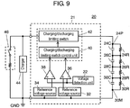
- FIG. 9 shows a configuration of conventional electric storage device 20.
- Electric storage device 20 includes charging/discharging limiting circuit 21.
- Charging/discharging limiting circuit 21 includes voltage detection unit 22, reference voltage sources 32 and 34, voltage comparison units 36 and 38, charging/discharging limiting switch control unit 40, and charging/discharging limiting switch 42.
- Voltage detection unit 22 is provided so as to detect a voltage between plus-side terminal 24P of storage element 24C and minus-side terminal 30M of storage element 30C, the storage elements being connected in a plurality of serial stages.
- the inter-terminal voltages increase themselves, resulting in an increase in voltage of the storage elements as a whole which is generated between plus-side terminal 24P and minus-side terminal 30M.
- balance resistances 24R, 26R, 28R and 30R are contacted in parallel with storage elements 24C, 26C, 38C and 30C, respectively.
- the device is configured such that a lower-limit voltage and an upper-limit voltage, which are allowed during discharging and charging, are set in reference voltage sources 32 and 34 and compared in voltage comparison units 36 and 38 with a detection voltage detected by voltage detection unit 22, and the detection results are separately outputted to charging/discharging limiting switch control unit 40.
- the device is configured such that, when the detection voltage detected by voltage detection unit 22 falls below reference voltage source 32, discharging from the storage element is limited through charging/discharging limiting switch 42. When the detection voltage exceeds reference voltage source 34, charging to the storage element is limited through charging/discharging limiting switch 42. It is to be noted that charging is performed by charger 44 and discharging is performed by external load 46.
- the present invention is to overcome such a problem, and to provide an electric storage device capable of alleviating or suppressing an influence of variations in internal resistance of the storage elements and concentration of a voltage which is transitionally generated by the charging current during charging to the storage element, to smoothly charge the storage elements, and reliably detect an overvoltage of each of the storage elements so as to prevent deterioration of the storage elements from occurring.
- Such an electric storage device of the present invention can eliminate an influence of variations in internal resistance of the storage elements and concentration of a voltage which is transitionally generated by the charging current during charging to the storage element, to smoothly charge the storage elements and reliably detect an overvoltage of each of the storage elements so as to prevent deterioration of the storage elements from occurring.
- FIGS. 1 to 8 constituents having an identical function are provided with an identical symbol and the description thereof will not be given.
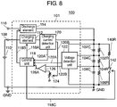
- FIG. 1 is a constitutional view of electric storage device 100 according to an embodiment 1.
- Electric storage device 100 includes charging/discharging limiting circuit 101.
- Charging/discharging limiting circuit 101 includes charge element 112, discharge element 114, control unit 118, charging current detection unit 120, voltage detection unit 122, valuable reference voltage source 124, and voltage comparison unit 126.
- valuable reference voltage source 124 is not in a conventional form where the magnitude of the voltage is fixed, but in a form where the magnitude of the voltage is automatically adjustable under control from some type of circuit unit.
- a plurality of storage elements 102C, 104C and 106C made up of electric double-layer capacitors are connected in serial.
- Storage elements 102C, 104C and 106C are connected in parallel with balance resistances 102R, 104R and 106R, respectively.
- Input terminal 108 is connected with direct current power source 110 as a charging current source, and configured so as to charge storage elements 102C, 104C and 106C through charge element 112 that limits a charging current. Namely, storage elements 102C, 104C and 106C are charged by direct current power source 110 through charge element 112 and charging current detection unit 120.
- Inter-terminal voltages V1, V2 and V3 that are generated in storage elements 102C, 104C and 106C are outputted to output terminal 116 through discharge element 114 that controls a discharging current.
- Charge element 112 and discharge element 114 are controlled so as to be activated based on control signal 118A and 118B outputted from control unit 118.
- control unit 118 generates control signals 118A and 118B based on detection signal 120A, 122A and 126A.
- Detection signal 120A is outputted from charging current detection unit 120 that detects a charging current of storage elements 102C, 104C and 106C.
- Detection signal 122A is outputted from voltage detection unit 122 that detects charging voltages of storage elements 102C, 104C and 106C.
- Detection signal 126A is outputted from voltage comparison unit 126 that compares valuable reference voltage source 124 with the discharging voltage.
- Charge element 112 is controlled by means of control signal 118A, and discharge element 114 is controlled by means of control signal 118B.
- Storage elements 102C, 104C and 106C are charged by a fixed charging current (constant current) in an initial stage of charging, and when charging proceeds and these storage elements reach a previously set voltage, charge element 112 is controlled based on control signal 118A so as to have a constant voltage. Further, in a case where certain irregularity occurs in storage elements 102C, 104C and 106C or in charging/discharging limiting circuit 101, valuable reference voltage source 124 is newly adjusted to have a prescribed magnitude by means of detection signal 120B taken out of charging current detection unit 120 so that the voltages that are applied to those storage elements do not exceed the resistance voltage. A comparison is made in voltage comparison unit 126 between newly adjusted valuable reference voltage source 124 and voltages corresponding to inter-terminal voltages V1, V2 and V3 of storage elements 102C, 104C and 106C.
- Valuable reference voltage source 124 is connected to an input terminal on a first side of voltage comparison unit 126. Detection signal 122B taken out of voltage detection unit 122 is connected to an input terminal on a second side of voltage comparison unit 126. Detection signal 122B is determined to be almost the same as the inter-terminal voltages of storage elements 102C, 104C and 106C, or be a voltage proportional to these voltages. Valuable reference voltage source 124 is compared with a detection signal taken out of voltage detection unit 122 in voltage comparison unit 126, and the comparison detection result is taken out of the output side of voltage comparison unit 126 as detection signal 126A.
- charge element 112 is controlled through control unit 118 and control signal 118A to halt the charging current or limit the magnitude of the charging current. This allows more reliable prevention of deterioration of storage elements 102C, 104C and 106C.
- voltage detection unit 122 may detect the entire voltage of the plurality of storage elements 102C, 104C and 106C, namely the magnitude of (V1 + V2 + V3), or at least one of the inter-terminal voltages of storage elements 102C, 104C and 106C, namely V1, V2 and V3. Further, the plurality of storage elements 102C, 104C and 106C may be grouped, and the sum or difference of any two of inter-terminal voltages V1, V2 and V3 may be detected.
- the embodiment 1 is characterized in that valuable reference voltage source 124 generates control signal 120B based on the charging current detected by charging current detection unit 120, and adjusts the magnitude of valuable reference voltage source 124 by means of control signal 120B.
- valuable reference voltage source 124 generates control signal 120B based on the charging current detected by charging current detection unit 120, and adjusts the magnitude of valuable reference voltage source 124 by means of control signal 120B.
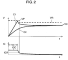
- FIG. 2 is a time chart during charging for explaining the characteristic of the electric storage device shown in FIG. 1 .
- a characteristic C1 shows a case where one internal resistance of one of storage elements 102C, 104C and 106C increases.
- Characteristic C2 shows an inter-terminal voltage of a storage element with a small internal resistance. This state can occur, for example, at a low temperature such as not higher than 0°C when variations in resistance value become larger.
- valuable reference voltage source 124 is previously set slightly higher at the initial stage of charging in consideration of peak voltage VP, and when charging current IC falls below current ICR as a prescribed threshold, the magnitude of valuable reference voltage source 124 is adjusted to be low through charging current detection unit 120 and control signal 120B. As thus described, when the magnitude of valuable reference voltage source 124 is adjusted based on the magnitude of charging current IC, it is possible to efficiently charge storage elements 102C, 104C and 106C while suppressing an influence of transitionally generated voltage concentration as much as possible.
- valuable reference voltage source 124 during charging can be set over resistance voltages (successively applicable voltages) of storage elements 102C, 104C and 106C. Such a setting may be made in consideration of the relation between the time at which valuable reference voltage source 124 transitionally exceeds the resistance voltage during charging and the lives of the electric double-layer capacitors constituting storage elements 102C, 104C and 106C.
- control unit, the voltage comparison unit and the variable reference voltage source may be constituted of a microcomputer or the like, and in that case, the variable reference voltage source can be set by software.
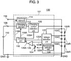
- FIG. 3 is a constitutional view of a storage element according to an embodiment 2. This is different from the embodiment 1 in that valuable reference voltage source 124 is adjusted based on temperatures of storage elements 102C, 104C and 106C themselves or ambient temperatures of a position where these storage elements are placed.
- temperature detection unit 130 is provided for detecting the temperature of at least one of storage elements 102C, 104C and 106C and the ambient temperatures of these storage elements.
- Detection signal 130A is generated based on a temperature detected by temperature detection unit 130, and valuable reference voltage source 124 is adjusted based on detection signal 130A.
- the internal resistances of storage elements 102C, 104C and 106C made up of the electric double-layer capacitors increase and variations in internal resistance become larger.
- peak voltage VP is generated since the voltage concentrates on that storage element, as shown in FIG. 2 .
- the resistance voltages (successively applicable voltages) of the electric double-layer capacitors constituting storage elements 102C, 104C and 106C are not significantly affected by the lives of the electric double-layer capacitors so long as being in a range of a certain magnitude.
- This can make valuable reference voltage source 124 larger regardless of the magnitude of the charging current with respect to the storage elements.
- how much valuable reference voltage source 124 is made larger may be determined in consideration of the relation between the temperature in an atmosphere where the storage elements are used and the lives of the electric double-layer capacitors.
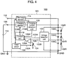
- FIG. 4 is a constitutional view of an electric storage device according to an embodiment 3. This is different from the embodiment 1 in that timer circuit 132 is provided in charging/discharging limiting circuit 101, and the magnitude of valuable reference voltage source 124 is adjusted by control signal 132A generated based on the time measured by timer circuit 132.
- the time from the start of charging is measured by timer circuit 132 and after the time has reached the calculated time to the completion of charging, the magnitude of valuable reference voltage source 124 is adjusted to be lower, so that the problem of peak voltage VP limiting charging current IC is eliminated and the storage elements can be smoothly charged.
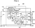
- FIG. 5 is a constitutional view of an electric storage device according to an embodiment 4. This is different from the embodiment 1 in that voltage storage unit 134 is provided which stores differences of the inter-terminal voltages which are stored in storage elements 102C, 104C and 106C before and after the halt of charging, e.g. (V1 - V2), (V2 - V3), (V3 - V1), to adjust valuable reference voltage source 124 through control signal 134A based on the differences of the voltages of the storage elements before and after the halt of charging.
- V1 - V2 differences of the inter-terminal voltages which are stored in storage elements 102C, 104C and 106C before and after the halt of charging
- V1 - V2 differences of the inter-terminal voltages which are stored in storage elements 102C, 104C and 106C before and after the halt of charging
- V1 - V2 differences of the inter-terminal voltages which are stored in storage elements 102C, 104C and 106C
- charging is temporarily halted during constant-current charging, and the difference in storage element voltage before and after the halt of charging is stored in voltage storage unit 134, to calculate peak voltage VP that is generated with a value of a product of the internal resistance of each of the storage elements and charging current IC.
- valuable reference voltage source 124 during constant-current charging is adjusted to increase so that the problem of charging current IC being limited due to generation of peak voltage VP is eliminated and the storage elements can be smoothly charged.
- FIG. 6 is a constitutional view of an electric storage device according to an embodiment 5. This is different from the embodiment 1 in that a voltage, detected by voltage detection unit 122 that detects inter-terminal voltages V1, V2 and V3 of storage elements 102C, 104C and 106C, is adjusted to the magnitude of valuable reference voltage source 124 through detection signal 122C. Namely, valuable reference voltage source 124 is adjusted by two control channel: first control through charging current detection unit 120 and control signal 120B; and second control through voltage detection unit 122 and detection signal 122C.
- charging current detection unit 120 adjusts valuable reference voltage source 124 based on charging current IC.
- valuable reference voltage source 124 is adjusted to a wrong magnitude due to malfunction.
- charging current IC is limited based on wrong valuable reference voltage source 124.
- the voltages of storage elements 102C, 104C and 106C detected by voltage detection unit 122 are added as one condition for adjustment of valuable reference voltage source 124, the problem of the change in magnitude of valuable reference voltage source 124 under the influence of a noise can be eliminated.
- a setting is made such that, when the inter-terminal voltages of storage elements 102C, 104C and 106C do not exceed a prescribed threshold, adjustment of valuable reference voltage source 124 is not executed. This can give redundancy against a noise so that an electric storage device with higher reliability can be provided.
- FIG. 7 is a constitutional view of an electric storage device according to an embodiment 6. This is different from the embodiment 1 in that, when the voltages of storage elements 102C, 104C and 106C exceed a set upper limit voltage, irregular signal generation circuit 136 which outputs an irregular signal is provided. With such a configuration, when certain irregularity occurs in the electric storage device and an overvoltage is applied to storage elements 102C, 104C and 106C, charging current IC is halted or limited to prevent deterioration of the these storage elements from occurring. In conjunction with this, an irregular signal is outputted to irregular signal terminal 138 to notify the user that the electric storage device is in an irregular state.
- FIG. 8 is a constitutional view of an electric storage device according to an embodiment 7. This is different from the embodiment 1 in that a discharge circuit unit made up of discharge resistance 140R and discharge switch 142 is provided. Namely, when a voltage applied to the electric double-layer capacitors as storage elements 102C, 104C and 106C are about to exceed a prescribed upper limit voltage, discharge switch 142 is closed to discharge a charge stacked in the whole of the electric double-layer capacitors through discharge resistance 140R in order to prevent deterioration of the electric double-layer capacitors from occurring. With this configuration, electric safety of the electric storage devices can be secured, and the lives thereof can further be extended.
- the electric storage device can eliminate an influence of variations in internal resistance of the storage elements and concentration of a voltage which is transitionally generated by a charging current during charging to the storage element. Further, the storage element is smoothly charged, and an overvoltage of each of the storage elements is reliably detected so that deterioration of the storage element can be prevented. Therefore, the electric storage device according to the present invention is useful for a backup power source for emergency that requires rapid charging by a large current, and hence the industrial applicability thereof is high.
Description
- The present invention relates to an electric storage device, configured by connecting a plurality of storage elements in serial or in series parallel, and having a charging/discharging limiting circuit function of detecting an overvoltage of the storage elements to prevent a deterioration of the storage elements.
- In a case where electric double-layer capacitors as storage elements are serially connected and then used, conventionally, a life of each storage elements has a large influence on a voltage applied to each storage element. Therefore, when variations in charging voltage of the storage elements occur, a reliability of the life as a whole of the electric storage devices may be degraded, and hence the voltage of each storage element is constantly monitored.
-
FIG. 9 shows a configuration of conventionalelectric storage device 20.Electric storage device 20 includes charging/discharging limitingcircuit 21. Charging/discharging limitingcircuit 21 includesvoltage detection unit 22,reference voltage sources voltage comparison units switch control unit 40, and charging/discharging limiting switch 42. -
Voltage detection unit 22 is provided so as to detect a voltage between plus-side terminal 24P ofstorage element 24C and minus-side terminal 30M ofstorage element 30C, the storage elements being connected in a plurality of serial stages. Whenstorage elements side terminal 24P and minus-side terminal 30M. It is to be noted thatbalance resistances storage elements - When these storage elements are over-discharged, the inter-terminal voltages of the storage elements decrease, and the voltage of the storage elements as a whole which is generated between plus-
side terminal 24P and minus-side terminal 30M also decreases. - Further, the device is configured such that a lower-limit voltage and an upper-limit voltage, which are allowed during discharging and charging, are set in
reference voltage sources voltage comparison units voltage detection unit 22, and the detection results are separately outputted to charging/discharging limitingswitch control unit 40. - Here, the device is configured such that, when the detection voltage detected by
voltage detection unit 22 falls belowreference voltage source 32, discharging from the storage element is limited through charging/discharginglimiting switch 42. When the detection voltage exceedsreference voltage source 34, charging to the storage element is limited through charging/discharginglimiting switch 42. It is to be noted that charging is performed bycharger 44 and discharging is performed byexternal load 46. - Moreover, as prior art documents relating to the invention of this application, for example, Unexamined Japanese Patent Publication No.
2000-197277 US5726552A are known. - However, in a conventional configuration, in a case where an internal resistances (not shown) of
storage elements reference voltage source 34, and every time that occurs, the charging current is limited, which causes a problem of taking time for charging. - In order to eliminate such a problem, for example in the low temperature atmosphere not higher than 0°C, it is necessary to take measures such as measuring electric characteristics of the storage elements to perform a selecting operation according to the levels of the characteristics, or increasing the number of serially connected storage elements for securing a resistance voltage. However, it is impossible to say that such measures are the optimum methods since causing a cost increase. Further, the larger the charging current, the more significantly such a tendency appears in the low temperature atmosphere, thereby bringing the electric storage device with a large current capacitance into even more disadvantageous state.
- The present invention is to overcome such a problem, and to provide an electric storage device capable of alleviating or suppressing an influence of variations in internal resistance of the storage elements and concentration of a voltage which is transitionally generated by the charging current during charging to the storage element, to smoothly charge the storage elements, and reliably detect an overvoltage of each of the storage elements so as to prevent deterioration of the storage elements from occurring.
- The electric storage device of the present invention is defined by the appended claims. Such an electric storage device of the present invention can eliminate an influence of variations in internal resistance of the storage elements and concentration of a voltage which is transitionally generated by the charging current during charging to the storage element, to smoothly charge the storage elements and reliably detect an overvoltage of each of the storage elements so as to prevent deterioration of the storage elements from occurring.
-
-
FIG. 1 is a constitutional view of an electric storage device according to anembodiment 1 of the present invention. -
FIG. 2 is a time chart according to theembodiment 1 of the present invention. -
FIG. 3 is a constitutional view of an electric storage device according to an embodiment 2 of the present invention. -
FIG. 4 is a constitutional view of an electric storage device according to an embodiment 3 of the present invention. -
FIG. 5 is a constitutional view of an electric storage device according to an embodiment 4 of the present invention. -
FIG. 6 is a constitutional view of an electric storage device according to an embodiment 5 of the present invention. -
FIG. 7 is a constitutional view of an electric storage device according to an embodiment 6 of the present invention. -
FIG. 8 is a constitutional view of an electric storage device according to an embodiment 7 of the present invention. -
FIG. 9 is a constitutional view of a conventional electric storage device. -
- 20, 100 Storage device
- 21, 101 Charging/discharging limiting circuit
- 24C, 26C, 28C, 30C, 102C, 104C, 106C Storage element
- 24P Plus-side terminal
- 30M Minus-side terminal
- 22 Voltage detection unit
- 32, 34 Reference voltage source
- 36, 38 Voltage comparison unit
- 40 Charging/discharging limiting switch control unit
- 42 Charging/discharging
limiting switch 44 Charger - 46 External load
- 108 Input terminal
- 110 Direct current power source
- 116 Output terminal
- 112 Charging element
- 120 Charging current detection unit
- 114 Discharge element
- 118 Control unit
- 126 Voltage comparison unit
- 124 Variable reference voltage source
- 122 Voltage detection unit
- 24R, 26R, 28R, 30R, 102R, 104R, 106R Balance resistance
- 130 Temperature detection unit
- 132 Timer circuit
- 134 Voltage storage unit
- 136 Irregular signal generation circuit
- 138 Irregular signal terminal
- 140R Discharge resistance
- 142 Discharge switch
- In the following, embodiments of the present invention are described with reference to drawings. In
FIGS. 1 to 8 , constituents having an identical function are provided with an identical symbol and the description thereof will not be given. -
FIG. 1 is a constitutional view ofelectric storage device 100 according to anembodiment 1.Electric storage device 100 includes charging/discharging limitingcircuit 101. Charging/discharging limitingcircuit 101 includescharge element 112,discharge element 114,control unit 118, chargingcurrent detection unit 120,voltage detection unit 122, valuablereference voltage source 124, andvoltage comparison unit 126. Here, valuablereference voltage source 124 is not in a conventional form where the magnitude of the voltage is fixed, but in a form where the magnitude of the voltage is automatically adjustable under control from some type of circuit unit. - A plurality of
storage elements Storage elements balance resistances Input terminal 108 is connected with directcurrent power source 110 as a charging current source, and configured so as to chargestorage elements charge element 112 that limits a charging current. Namely,storage elements current power source 110 throughcharge element 112 and chargingcurrent detection unit 120. - Inter-terminal voltages V1, V2 and V3 that are generated in
storage elements output terminal 116 throughdischarge element 114 that controls a discharging current.Charge element 112 anddischarge element 114 are controlled so as to be activated based oncontrol signal control unit 118. Further,control unit 118 generatescontrol signals detection signal Detection signal 120A is outputted from chargingcurrent detection unit 120 that detects a charging current ofstorage elements Detection signal 122A is outputted fromvoltage detection unit 122 that detects charging voltages ofstorage elements Detection signal 126A is outputted fromvoltage comparison unit 126 that compares valuablereference voltage source 124 with the discharging voltage.Charge element 112 is controlled by means ofcontrol signal 118A, anddischarge element 114 is controlled by means ofcontrol signal 118B. -
Storage elements charge element 112 is controlled based oncontrol signal 118A so as to have a constant voltage. Further, in a case where certain irregularity occurs instorage elements circuit 101, valuablereference voltage source 124 is newly adjusted to have a prescribed magnitude by means ofdetection signal 120B taken out of chargingcurrent detection unit 120 so that the voltages that are applied to those storage elements do not exceed the resistance voltage. A comparison is made involtage comparison unit 126 between newly adjusted valuablereference voltage source 124 and voltages corresponding to inter-terminal voltages V1, V2 and V3 ofstorage elements - Valuable
reference voltage source 124 is connected to an input terminal on a first side ofvoltage comparison unit 126.Detection signal 122B taken out ofvoltage detection unit 122 is connected to an input terminal on a second side ofvoltage comparison unit 126.Detection signal 122B is determined to be almost the same as the inter-terminal voltages ofstorage elements reference voltage source 124 is compared with a detection signal taken out ofvoltage detection unit 122 involtage comparison unit 126, and the comparison detection result is taken out of the output side ofvoltage comparison unit 126 asdetection signal 126A. - When inter-terminal voltages V1, V2 and V3 of
storage elements reference voltage source 124,charge element 112 is controlled throughcontrol unit 118 and control signal 118A to halt the charging current or limit the magnitude of the charging current. This allows more reliable prevention of deterioration ofstorage elements - It is to be noted that
voltage detection unit 122 may detect the entire voltage of the plurality ofstorage elements storage elements storage elements - The
embodiment 1 is characterized in that valuablereference voltage source 124 generatescontrol signal 120B based on the charging current detected by chargingcurrent detection unit 120, and adjusts the magnitude of valuablereference voltage source 124 by means ofcontrol signal 120B. Such a characteristic apparently differs from that of the conventional electric storage device with a fixed reference voltage power. -
FIG. 2 is a time chart during charging for explaining the characteristic of the electric storage device shown inFIG. 1 . InFIG. 2 , a characteristic C1 shows a case where one internal resistance of one ofstorage elements FIG. 2 is generated, exceeding reference voltage VR, and with the passage of time t, as charging by constant current ICC is shifted to control by a constant voltage, charging current IC gradually decreases, and peak voltage VP also gradually decreases and ultimately converges to prescribed magnitude VC. - In the
embodiment 1, valuablereference voltage source 124 is previously set slightly higher at the initial stage of charging in consideration of peak voltage VP, and when charging current IC falls below current ICR as a prescribed threshold, the magnitude of valuablereference voltage source 124 is adjusted to be low through chargingcurrent detection unit 120 and control signal 120B. As thus described, when the magnitude of valuablereference voltage source 124 is adjusted based on the magnitude of charging current IC, it is possible to efficiently chargestorage elements - It is to be noted that valuable
reference voltage source 124 during charging can be set over resistance voltages (successively applicable voltages) ofstorage elements reference voltage source 124 transitionally exceeds the resistance voltage during charging and the lives of the electric double-layer capacitors constitutingstorage elements - It is to be noted that in the
embodiment 1, the case of serially connecting threestorage elements -
FIG. 3 is a constitutional view of a storage element according to an embodiment 2. This is different from theembodiment 1 in that valuablereference voltage source 124 is adjusted based on temperatures ofstorage elements - Namely,
temperature detection unit 130 is provided for detecting the temperature of at least one ofstorage elements Detection signal 130A is generated based on a temperature detected bytemperature detection unit 130, and valuablereference voltage source 124 is adjusted based ondetection signal 130A. - At a low temperature such as not higher than 0°C, the internal resistances of
storage elements storage elements FIG. 2 . - It is to be noted that at a low temperature, the resistance voltages (successively applicable voltages) of the electric double-layer capacitors constituting
storage elements reference voltage source 124 larger regardless of the magnitude of the charging current with respect to the storage elements. In addition, how much valuablereference voltage source 124 is made larger may be determined in consideration of the relation between the temperature in an atmosphere where the storage elements are used and the lives of the electric double-layer capacitors. -
FIG. 4 is a constitutional view of an electric storage device according to an embodiment 3. This is different from theembodiment 1 in thattimer circuit 132 is provided in charging/discharging limitingcircuit 101, and the magnitude of valuablereference voltage source 124 is adjusted bycontrol signal 132A generated based on the time measured bytimer circuit 132. - Namely, as seen from the time chart shown in
FIG. 2 , it is during period tcc when charging is performed by constant current ICC that peak voltage VP is generated instorage elements - Therefore, the time from the start of charging is measured by
timer circuit 132 and after the time has reached the calculated time to the completion of charging, the magnitude of valuablereference voltage source 124 is adjusted to be lower, so that the problem of peak voltage VP limiting charging current IC is eliminated and the storage elements can be smoothly charged. -
FIG. 5 is a constitutional view of an electric storage device according to an embodiment 4. This is different from theembodiment 1 in thatvoltage storage unit 134 is provided which stores differences of the inter-terminal voltages which are stored instorage elements reference voltage source 124 throughcontrol signal 134A based on the differences of the voltages of the storage elements before and after the halt of charging. - Namely, charging is temporarily halted during constant-current charging, and the difference in storage element voltage before and after the halt of charging is stored in
voltage storage unit 134, to calculate peak voltage VP that is generated with a value of a product of the internal resistance of each of the storage elements and charging current IC. Based upon this, valuablereference voltage source 124 during constant-current charging is adjusted to increase so that the problem of charging current IC being limited due to generation of peak voltage VP is eliminated and the storage elements can be smoothly charged. -
FIG. 6 is a constitutional view of an electric storage device according to an embodiment 5. This is different from theembodiment 1 in that a voltage, detected byvoltage detection unit 122 that detects inter-terminal voltages V1, V2 and V3 ofstorage elements reference voltage source 124 throughdetection signal 122C. Namely, valuablereference voltage source 124 is adjusted by two control channel: first control through chargingcurrent detection unit 120 andcontrol signal 120B; and second control throughvoltage detection unit 122 anddetection signal 122C. - In the
embodiment 1, chargingcurrent detection unit 120 adjusts valuablereference voltage source 124 based on charging current IC. In such a configuration, there may occur a problem in that, when a noise is applied to charging current IC, valuablereference voltage source 124 is adjusted to a wrong magnitude due to malfunction. At this time, charging current IC is limited based on wrong valuablereference voltage source 124. As opposed to this, in the embodiment 5, since the voltages ofstorage elements voltage detection unit 122 are added as one condition for adjustment of valuablereference voltage source 124, the problem of the change in magnitude of valuablereference voltage source 124 under the influence of a noise can be eliminated. Namely, a setting is made such that, when the inter-terminal voltages ofstorage elements reference voltage source 124 is not executed. This can give redundancy against a noise so that an electric storage device with higher reliability can be provided. -
FIG. 7 is a constitutional view of an electric storage device according to an embodiment 6. This is different from theembodiment 1 in that, when the voltages ofstorage elements signal generation circuit 136 which outputs an irregular signal is provided. With such a configuration, when certain irregularity occurs in the electric storage device and an overvoltage is applied tostorage elements irregular signal terminal 138 to notify the user that the electric storage device is in an irregular state. - It is to be noted that the characteristic of the embodiment 6 can also be applied to the embodiments 2 to 5, and a similar effect is exerted.
-
FIG. 8 is a constitutional view of an electric storage device according to an embodiment 7. This is different from theembodiment 1 in that a discharge circuit unit made up ofdischarge resistance 140R anddischarge switch 142 is provided. Namely, when a voltage applied to the electric double-layer capacitors asstorage elements discharge switch 142 is closed to discharge a charge stacked in the whole of the electric double-layer capacitors throughdischarge resistance 140R in order to prevent deterioration of the electric double-layer capacitors from occurring. With this configuration, electric safety of the electric storage devices can be secured, and the lives thereof can further be extended. - It is to be noted that the configuration according to the embodiment 7 can also be applied to the configurations of the embodiments 2 to 5, and a similar effect is exerted.
- The electric storage device according to the present invention can eliminate an influence of variations in internal resistance of the storage elements and concentration of a voltage which is transitionally generated by a charging current during charging to the storage element. Further, the storage element is smoothly charged, and an overvoltage of each of the storage elements is reliably detected so that deterioration of the storage element can be prevented. Therefore, the electric storage device according to the present invention is useful for a backup power source for emergency that requires rapid charging by a large current, and hence the industrial applicability thereof is high.
Claims (3)
- An electric storage device (100), comprising:an input terminal (108);a direct current power source (110) connected to the input terminal;a charge element (112) connected to the input terminal and limiting a direct current from the direct current power source; a charging current detection unit (120) connected to the charge element (112) and adapted to detect a charging current; a plurality of storage elements (102C, 104C, 106C) connected to the charging current detection unit, said storage elements being connected in serial or in series parallel connection;a discharge element (114) connected to the plurality of storage elements;an output terminal (116) connected to the discharge element;a voltage detection unit (122) configured to detect the entire voltage of the plurality of storage elements (102C, 104C and 106C) or at least one of the inter-terminal voltages of the plurality of storage elements (102C, 104C and 106C); the inter-terminal voltage being the voltage across each storage element; a control unit (118) connected to the voltage detection unit and controlling the charge element and the discharge element;a voltage comparison unit (126) connected to the voltage detection unit and the control unit;characterized in that the electric storage device further comprisesa variable reference voltage source (124) connected to the voltage comparison unit, and its magnitude is adjusted therefor,wherein the magnitude of the variable reference voltage source (124) is adjusted so as to be higher at an initial stage of charging compared to the magnitude of the reference voltage at a subsequent stage of charging, based on an element of the group comprising:- a charging current value detected by the charging current detection unit (120);- a temperature of at least one of the storage elements or an ambient temperature of a position where the storage elements are placed;- a time measured by a timer circuit (132) connected to the control unit (118);- differences of the inter-terminal voltages of the storage elements before and after a halt of the charging, said charging of the storage elements being temporarily halted during the charging;wherein, when a detection signal (122B) taken out of the voltage detection unit (122) exceeds the variable reference voltage source, an overvoltage is detected and the charge element is controlled through the control unit to halt the charging current or to limit a magnitude of the charging current, so as to prevent deterioration of at least one of the plurality of storage elements.
- The electric storage device (100) according to claim 1, comprising:an irregular signal generation circuit (136) which is adapted to output an irregular signal when the voltages of the plurality of storage elements (102C,104C, 106C) exceed a set upper limit voltage, whereby the irregular signal is output to notify the user that the electric storage device is in an irregular state.
- The electric storage device (100) according to claim 1, comprising:a discharge circuit unit (140R, 142) adapted to discharge a charge which has been stored in the storage elements (102C, 104C, 106C) when a voltage applied to the storage elements exceeds a prescribed upper limit voltage,wherein the storage elements are constituted with electric double layered capacitors.
Applications Claiming Priority (2)
| Application Number | Priority Date | Filing Date | Title |
|---|---|---|---|
| JP2005142640A JP4367374B2 (en) | 2005-05-16 | 2005-05-16 | Power storage device |
| PCT/JP2006/309631 WO2006123598A1 (en) | 2005-05-16 | 2006-05-15 | Electric storage device |
Publications (3)
| Publication Number | Publication Date |
|---|---|
| EP1883144A1 EP1883144A1 (en) | 2008-01-30 |
| EP1883144A4 EP1883144A4 (en) | 2011-05-18 |
| EP1883144B1 true EP1883144B1 (en) | 2017-11-29 |
Family
ID=37431171
Family Applications (1)
| Application Number | Title | Priority Date | Filing Date |
|---|---|---|---|
| EP06746378.6A Active EP1883144B1 (en) | 2005-05-16 | 2006-05-15 | Electric storage device |
Country Status (5)
| Country | Link |
|---|---|
| US (1) | US7777456B2 (en) |
| EP (1) | EP1883144B1 (en) |
| JP (1) | JP4367374B2 (en) |
| CN (1) | CN101176246B (en) |
| WO (1) | WO2006123598A1 (en) |
Families Citing this family (27)
| Publication number | Priority date | Publication date | Assignee | Title |
|---|---|---|---|---|
| US20100259210A1 (en) * | 2005-10-20 | 2010-10-14 | Nissan Diesel Motor Co., Ltd. | Charged/Discharged Power control for a Capacitor Type Energy Storage Device |
| JP2008182809A (en) * | 2007-01-24 | 2008-08-07 | Matsushita Electric Ind Co Ltd | Battery circuit, battery pack, and battery system |
| JP5455174B2 (en) * | 2007-08-02 | 2014-03-26 | 鹿島建設株式会社 | Wireless power receiving adapter |
| FR2926934B1 (en) * | 2008-01-29 | 2010-09-17 | Saft Groupe Sa | ELECTRONIC SYSTEM FOR BATTERY |
| CN101784151B (en) * | 2009-01-16 | 2013-11-06 | 国琏电子(上海)有限公司 | Light source driving device |
| JP5304279B2 (en) * | 2009-01-30 | 2013-10-02 | パナソニック株式会社 | Power storage device |
| US20100244785A1 (en) * | 2009-03-27 | 2010-09-30 | Applied Micro Circuits Corporation | Source Power Limiting Charging System |
| JP5390925B2 (en) * | 2009-04-24 | 2014-01-15 | パナソニック株式会社 | Battery pack |
| WO2011013472A1 (en) * | 2009-07-31 | 2011-02-03 | 本田技研工業株式会社 | Apparatus for managing electricity storage capacity |
| JP2011229279A (en) * | 2010-04-20 | 2011-11-10 | Rohm Co Ltd | Charging control device |
| CN102270858A (en) * | 2010-06-01 | 2011-12-07 | 硕颉科技股份有限公司 | Charging device |
| CN103493351B (en) | 2010-12-22 | 2017-10-24 | 通用电气能源能量变换技术有限公司 | The mechanical device of many level power converter circuits |
| WO2012087895A1 (en) | 2010-12-22 | 2012-06-28 | Converteam Technology Ltd. | Capacitor balancing circuit and control method for an electronic device such as a multilevel power inverter |
| US20130278221A1 (en) * | 2010-12-28 | 2013-10-24 | Reizo Maeda | Method of detecting battery degradation level |
| US8742729B2 (en) * | 2011-06-07 | 2014-06-03 | Flashsilicon Incorporation | Rechargeable battery |
| US20140132002A1 (en) * | 2011-08-24 | 2014-05-15 | Panasonic Corporation | Vehicle power source device |
| EP2805401B1 (en) * | 2012-01-16 | 2015-12-30 | Schneider Electric Buildings LLC | Adjustment of a capacitor charge voltage |
| US9991723B2 (en) * | 2012-09-17 | 2018-06-05 | The Boeing Company | Virtual cell method for battery management |
| CN203337806U (en) * | 2013-08-01 | 2013-12-11 | 向智勇 | Electric quantity inquiring device |
| WO2017002292A1 (en) * | 2015-06-30 | 2017-01-05 | ソニー株式会社 | Power storage system, controller, and storage battery charging and discharging method |
| JP2018026937A (en) * | 2016-08-09 | 2018-02-15 | 日立オートモティブシステムズ株式会社 | Power converter |
| JP7172857B2 (en) * | 2019-05-28 | 2022-11-16 | 株式会社デンソー | Control device |
| US11710970B2 (en) | 2020-01-17 | 2023-07-25 | BWR Innovations LLC | Remotely controlled electrical power generating system |
| US11018508B1 (en) * | 2020-01-17 | 2021-05-25 | BWR Innovations LLC | Electrical power generating system |
| US20220407332A1 (en) * | 2021-06-21 | 2022-12-22 | Lenovo (United States) Inc. | Charging control method of a battery pack for portable electronic devices |
| US11945338B2 (en) | 2021-08-13 | 2024-04-02 | BWR Innovations LLC | Fuel cell auxiliary power generation system for a vehicle |
| CN114189013A (en) * | 2021-11-30 | 2022-03-15 | 华为数字能源技术有限公司 | Charging device, charging method and computer readable storage medium |
Family Cites Families (14)
| Publication number | Priority date | Publication date | Assignee | Title |
|---|---|---|---|---|
| JPS63110926A (en) * | 1986-10-27 | 1988-05-16 | カシオ計算機株式会社 | Charging informer |
| JPH05219663A (en) * | 1992-01-31 | 1993-08-27 | Kyocera Corp | Solar light power generating system |
| JPH0799723A (en) * | 1993-09-28 | 1995-04-11 | Okamura Kenkyusho:Kk | Power capacitance device |
| US5545933A (en) | 1993-09-28 | 1996-08-13 | Okamura Laboratory Inc. | Electric power storage apparatus |
| JPH07288938A (en) * | 1994-04-11 | 1995-10-31 | Omron Corp | Battery charging apparatus |
| JP3174472B2 (en) * | 1995-02-27 | 2001-06-11 | 株式会社岡村研究所 | Parallel charge control device, power storage device, and charge control method |
| TW407212B (en) * | 1997-10-31 | 2000-10-01 | Toshiba Battery | Battery remaining capacity measuring device |
| EP0982830A3 (en) * | 1998-08-21 | 2001-03-21 | Sony Corporation | Battery pack |
| JP2000197277A (en) * | 1998-12-25 | 2000-07-14 | Asahi Glass Co Ltd | Power supply unit with built-in electric double-layer capacitor |
| JP3638109B2 (en) * | 2000-02-07 | 2005-04-13 | Necトーキン栃木株式会社 | Battery pack |
| DE10007417A1 (en) * | 2000-02-18 | 2001-09-13 | Epcos Ag | Circuit structure for suppressing excess-voltage as a Helmholtz effect includes a chain consisting of double-layer capacitors and modules connected parallel to the double-layer capacitors |
| US20030214267A1 (en) * | 2002-05-20 | 2003-11-20 | Long Laurence P. | Ultracapacitor balancing circuit |
| CN2613916Y (en) * | 2003-03-28 | 2004-04-28 | 徐玉琴 | Intelligent protector for accumulator |
| JP2006145285A (en) * | 2004-11-17 | 2006-06-08 | Ricoh Co Ltd | Battery residual charge detector |
-
2005
- 2005-05-16 JP JP2005142640A patent/JP4367374B2/en active Active
-
2006
- 2006-05-15 CN CN2006800168824A patent/CN101176246B/en active Active
- 2006-05-15 EP EP06746378.6A patent/EP1883144B1/en active Active
- 2006-05-15 US US11/918,252 patent/US7777456B2/en active Active
- 2006-05-15 WO PCT/JP2006/309631 patent/WO2006123598A1/en active Application Filing
Non-Patent Citations (1)
| Title |
|---|
| None * |
Also Published As
| Publication number | Publication date |
|---|---|
| EP1883144A1 (en) | 2008-01-30 |
| US20090072791A1 (en) | 2009-03-19 |
| EP1883144A4 (en) | 2011-05-18 |
| US7777456B2 (en) | 2010-08-17 |
| JP4367374B2 (en) | 2009-11-18 |
| WO2006123598A1 (en) | 2006-11-23 |
| JP2006320170A (en) | 2006-11-24 |
| CN101176246B (en) | 2011-04-13 |
| CN101176246A (en) | 2008-05-07 |
Similar Documents
| Publication | Publication Date | Title |
|---|---|---|
| EP1883144B1 (en) | Electric storage device | |
| US11913998B2 (en) | Management device and power supply system | |
| US7880444B2 (en) | Process for balanced charging of a lithium ion or lithium polymer battery | |
| US8547064B2 (en) | Battery cell tab monitor | |
| EP2838152B1 (en) | Discharging device for electricity storage device | |
| US10211490B2 (en) | Storage battery deterioration measurement device and power storage system | |
| JP4932975B2 (en) | Overcurrent detection circuit and battery pack | |
| US7482816B2 (en) | Voltage monitor and electrical storage device using the same | |
| JP4682037B2 (en) | Insulation detector | |
| JP5326973B2 (en) | Battery monitoring device | |
| US20180306845A1 (en) | Voltage measuring apparatus, voltage measuring method, voltage control apparatus, and voltage control method | |
| WO2014045567A1 (en) | Power source device, and electric vehicle and power accumulation device provided with said power source device | |
| US20150048795A1 (en) | Charge control apparatus and charge control method | |
| US11493564B2 (en) | Ground fault detection device | |
| US20080218176A1 (en) | Power Supply Device | |
| US10845419B2 (en) | Assembled battery circuit, capacitance coefficient detection method, and capacitance coefficient detection program | |
| KR102349705B1 (en) | Battery cell balancing circuit and apparatus and method for balancing of a battery cell for using the same | |
| US9257852B2 (en) | Battery pack and method of controlling the same | |
| JP6598209B2 (en) | Voltage detector | |
| JPH0787673A (en) | Charging controlling system | |
| JP4440717B2 (en) | DC voltage supply device | |
| JP6673035B2 (en) | Battery system | |
| US11824392B2 (en) | Battery pack | |
| JP2010246214A (en) | Device for regulating and monitoring battery voltage | |
| JP4218587B2 (en) | Battery pack capacity adjustment device |
Legal Events
| Date | Code | Title | Description |
|---|---|---|---|
| PUAI | Public reference made under article 153(3) epc to a published international application that has entered the european phase |
Free format text: ORIGINAL CODE: 0009012 |
|
| 17P | Request for examination filed |
Effective date: 20071018 |
|
| AK | Designated contracting states |
Kind code of ref document: A1 Designated state(s): DE FR IT |
|
| DAX | Request for extension of the european patent (deleted) | ||
| RBV | Designated contracting states (corrected) |
Designated state(s): DE FR IT |
|
| RAP1 | Party data changed (applicant data changed or rights of an application transferred) |
Owner name: PANASONIC CORPORATION |
|
| REG | Reference to a national code |
Ref country code: DE Ref legal event code: R079 Ref document number: 602006054225 Country of ref document: DE Free format text: PREVIOUS MAIN CLASS: H02J0007020000 Ipc: H02J0007000000 |
|
| A4 | Supplementary search report drawn up and despatched |
Effective date: 20110419 |
|
| RIC1 | Information provided on ipc code assigned before grant |
Ipc: H02J 7/00 20060101AFI20110413BHEP |
|
| 17Q | First examination report despatched |
Effective date: 20140410 |
|
| RAP1 | Party data changed (applicant data changed or rights of an application transferred) |
Owner name: PANASONIC INTELLECTUAL PROPERTY MANAGEMENT CO., LT |
|
| RAP1 | Party data changed (applicant data changed or rights of an application transferred) |
Owner name: PANASONIC INTELLECTUAL PROPERTY MANAGEMENT CO., LT |
|
| STAA | Information on the status of an ep patent application or granted ep patent |
Free format text: STATUS: EXAMINATION IS IN PROGRESS |
|
| GRAP | Despatch of communication of intention to grant a patent |
Free format text: ORIGINAL CODE: EPIDOSNIGR1 |
|
| STAA | Information on the status of an ep patent application or granted ep patent |
Free format text: STATUS: GRANT OF PATENT IS INTENDED |
|
| INTG | Intention to grant announced |
Effective date: 20170628 |
|
| RIN1 | Information on inventor provided before grant (corrected) |
Inventor name: MORITA, KAZUKI Inventor name: TAKEMOTO, JUNJI Inventor name: ODAJIMA, YOSHIMITU |
|
| GRAS | Grant fee paid |
Free format text: ORIGINAL CODE: EPIDOSNIGR3 |
|
| GRAA | (expected) grant |
Free format text: ORIGINAL CODE: 0009210 |
|
| STAA | Information on the status of an ep patent application or granted ep patent |
Free format text: STATUS: THE PATENT HAS BEEN GRANTED |
|
| AK | Designated contracting states |
Kind code of ref document: B1 Designated state(s): DE FR IT |
|
| REG | Reference to a national code |
Ref country code: DE Ref legal event code: R096 Ref document number: 602006054225 Country of ref document: DE |
|
| REG | Reference to a national code |
Ref country code: DE Ref legal event code: R097 Ref document number: 602006054225 Country of ref document: DE |
|
| PG25 | Lapsed in a contracting state [announced via postgrant information from national office to epo] |
Ref country code: IT Free format text: LAPSE BECAUSE OF FAILURE TO SUBMIT A TRANSLATION OF THE DESCRIPTION OR TO PAY THE FEE WITHIN THE PRESCRIBED TIME-LIMIT Effective date: 20171129 |
|
| PLBE | No opposition filed within time limit |
Free format text: ORIGINAL CODE: 0009261 |
|
| STAA | Information on the status of an ep patent application or granted ep patent |
Free format text: STATUS: NO OPPOSITION FILED WITHIN TIME LIMIT |
|
| 26N | No opposition filed |
Effective date: 20180830 |
|
| PG25 | Lapsed in a contracting state [announced via postgrant information from national office to epo] |
Ref country code: FR Free format text: LAPSE BECAUSE OF NON-PAYMENT OF DUE FEES Effective date: 20180531 |
|
| PGFP | Annual fee paid to national office [announced via postgrant information from national office to epo] |
Ref country code: DE Payment date: 20230519 Year of fee payment: 18 |